JP4395610B2 - Optical head with semiconductor laser - Google Patents
Optical head with semiconductor laser Download PDFInfo
- Publication number
- JP4395610B2 JP4395610B2 JP2000024201A JP2000024201A JP4395610B2 JP 4395610 B2 JP4395610 B2 JP 4395610B2 JP 2000024201 A JP2000024201 A JP 2000024201A JP 2000024201 A JP2000024201 A JP 2000024201A JP 4395610 B2 JP4395610 B2 JP 4395610B2
- Authority
- JP
- Japan
- Prior art keywords
- semiconductor laser
- optical
- optical head
- laser
- tip
- Prior art date
- Legal status (The legal status is an assumption and is not a legal conclusion. Google has not performed a legal analysis and makes no representation as to the accuracy of the status listed.)
- Expired - Fee Related
Links
Images


Description
【0001】
【発明の属する技術分野】
本発明は、半導体レーザを搭載し、近接場光を用いて光ディスクに情報の記録を行う光学ヘッドに関する。
【0002】
また、本発明は、半導体レーザおよび磁気抵抗素子を搭載し、近接場光を用いて情報の記録再生を行う光学ヘッドに関する。
【0003】
【従来の技術】
パソコンの外部記憶装置としてHDD、FDDなどの磁気記録、およびMO,CD−R,DVD−RAMなどの光記録があるが、何れも大容量化が望まれている。その理由として、(1)アプリケーションやOSの高機能化によりプログラムサイズが肥大化していること、(2)主記憶容量の増大につれて通常主記憶容量の1.5〜2倍確保する仮想記憶領域の増大及びCD−RAMなどのキャッシングにも数百MB必要になっていること、(3)インターネットの普及によりユーザが気付かない内に蓄積データが増加していること、(4)ディジタルビデオの普及により画像をディスクに記録する要求が増加していること、そして(5)各家庭用にサーバを設置する要求が有ることが上げられる。
【0004】
このような大容量化の要求に対して、MIG(Metal in Gap)ヘッド、薄膜ヘッドからMR(Magneto Resister)ヘッドの採用、さらには巨大磁気抵抗素子、即ちGMR(Giant Magneto Resister)ヘッドの採用によって磁気記録であるHDDの面記録密度は増加している。
【0005】
この大容量化の要求に対して、最近、米国のSeagate社が23.8Gb/in2の記録密度を達成している。
【0006】
一方、光ディスク記録は1972年にヒリップス社から民生用のHe−Neレーザ搭載のビデオディスクが発表されてから発展をとげ、現在では両面4層のDVDで18Gbyteの記録容量を達成している。
【0007】
また、最近では、高密度記録として、近接場光学応用によるナノプローブ技術が注目されている。ところが、ナノプローブの先端を尖鋭にすればするほど入射光に対する射出エバネセント波の光量比が7桁ないし9桁も減衰するのが実状である。
【0008】
【発明が解決しようとする課題】
従来の磁気記録では、磁気記録は極端に面記録密度を高めていくと、磁気記録層に書き込まれたスピンが熱磁気緩和現象によって経時変化と共にデータが消失すると言う問題があり、21世紀初頭には50Gb/in2〜100Gb/in2の記録密度が限界であると言われている。
【0009】
また、従来の光ディスク記録では、レーザ光をレンズなどを用いて絞り込んだときに、光波の回折現象によって光源であるレーザの波長程度にしかビーム径を絞り込めないので、410nmの紫外線レーザを使用しても面記録密度は20〜30Gb/in2程度が光記録の限界と言われている。更に、使用する高精度の光学部品は高価であり、コストアップになっている。即ち、磁気記録、光記録ともにまもなく記録密度の限界を迎えることになる。
【0010】
また、近接場光学応用によるナノプローブ技術も現在の光ディスクの記録密度以上の高面記録密度の近接場光学の応用の成果が得られていない。
【0011】
本発明の目的は、この問題を解決するため、レーザ光の光量が減衰することなく、近接場光学を用いて光ディスクに高密度記録できる光学ヘッドを提供することにある。
【0012】
【課題を解決するための手段】
現在得られる短波長半導体レーザ光として635nmの波長を使用し,この波長で透明でかつ,屈折率の高い半導体材料例えば,GaP結晶を用いて先端が90nmに尖鋭化させたピラミッド状の特殊光学プリズムを用い,635nmレーザ光を底面から入射させるとプリズム内での半波長が88nmとなる。したがってプリズム先端を90nm径の平坦面にしておけばまったく減衰なくレーザ光が射出する。この先端を光磁気ディスク媒体にコンタクトヘッドあるいはフライングヘッドの原理を用いて約50nm以下の間隔で保つことによりレンズを使わないでレンズを使用したよりも極めて小さなビームスポットを形成することができる。
【0013】
本発明は、半導体レーザの出力端面に高屈折率プリズム物質を設け、この先端部を直径90nmあるいは90nm角の平面に形成し、この先端と光記録媒体間を近接場光学が作用する距離に保ち光磁気記録媒体に対して記録を行う光学ヘッドを提供する。
【0014】
また、本発明は、半導体レーザ素子と、この半導体レーザ素子の出力端面に設けられる高屈折率台形形状プリズム物質とにより構成され、前記高屈折率台形形状プリズム物質の先端部を、入射させる光波の波長をλとし前記台形形状プリズム物質の屈折率をnとすると先端開口サイズがほぼλ/2nとなるように形成し、前記先端部と光記録媒体との間をλ/4波長以下のギャップとし、前記プリズム物質内部では通常の光波を殆ど減衰することなく伝搬させる、近接場光学により光磁気記録媒体に対して記録を行う光学ヘッドを提供する。
【0015】
また、本発明は、直径90nmあるいは90nm角の平面に形成された先端部を有する高屈折率プリズム(トンガリピラミッド)を出力端面に設け、高屈折率プリズムの物質内でレーザを発生する半導体レーザ素子と、この半導体レーザ素子と一体化される磁気抵抗素子とで構成され、プリズム状物質から光記録媒体間の僅かな距離のみは近接場光学により光記録媒体に対して高密度記録再生を行う光学ヘッドを提供する。
【0016】
また、本発明は、λ=650nm,n=3.3の場合には、直径90nmあるいは90nm角の平面に形成された先端部を有するトンガリピラミッドを出力端面に設けた半導体レーザ素子と、この半導体レーザ素子と一体化される磁気抵抗素子とで構成され、近接場光学により光記録媒体に対して高密度記録再生を行う光学ヘッドを提供する。
【0017】
また、本発明は、記録用の高屈折率台形形状プリズム形状物質をレーザ射出面に併設した半導体レーザに光記録媒体の記録済みビットからの反射光強度が半導体レーザへ戻ることによって得られるレーザの戻り光誘起雑音を検出する手段を含む光学ヘッドを提供する。
【0018】
本発明によると、波長の約1/10のサイズで光記録ができる。しかも、レーザー出力の殆ど100%を記録に使用できる。光記録媒体は,TbFeCoの垂直磁性媒体あるいはGeSbTeなどによる相変化記録媒体を用いる。このときの記録ビットの検出、即ち記録情報再生には2つの方法がある。第1の方法は、巨大磁気抵抗素子(GMR)を用いて磁化の変化を検出する方法である。第2の方法は、半導体レーザの出力部に薄い1/4波長板を設置し、半導体レーザーからの直線偏波を右回りの円偏波に変換させる。光磁気ディスクによって,反射位相がπrad変移して再び1/4波長板に戻る。この波長板を通過して、左回りの円偏波は、レーザーの中で直線偏波とはπ/2rad異なった(即ち,両者が直交した)直線偏波となる。光磁気信号によって,カー回転角が,両者に重畳される。言い換えれば、両者間に、カー回転による位相差を生ずる。この位相差は,光の周波数差となって現れる。高速フォトダイオードで,このビート信号を検出することによって,信号が再生できる。
【0019】
本発明において、記録再生ヘッドは、第1の方法では,半導体レーザチップ+GMRチップで構成される。第2の方法では,半導体レーザーチップ+特殊半導体レーザーチップで構成される。サイズはいずれも約1mm3程度である。これをハードディスクのフライングヘッドスライダーに取り付ける。磁気ディスクドライブとほぼ同じ大きさで,磁気ディスクドライブの3倍の面記録密度が実現する。3.5インチディスクで、30GBの大容量が実現できる。
【0020】
【発明の実施の形態】
図1は、本発明の一実施形態の光学ヘッドを示している。これによると、光学ヘッド11はディスクドライブモータ(図示せず)により回転される光磁気ディスク12に対向配置され、ヘッド位置移動用モータにより駆動されるサスペンション13の先端に取り付けられる。この光学ヘッド11と光磁気ディスク12との間隔は50nm以下に設定されることにより近接場光学により記録が行える。
【0021】
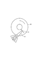
光学ヘッド11は、図2(a),(b)に示すように端面発光半導体レーザあるいはビクセルレーザ20により構成される。この半導体レーザ20は約635nmで発振する端面発光InGaAIP系のIII−V族化合物半導体レーザ素子21により構成される。この半導体レーザ素子21の出力端面に例えばGaP結晶で作成したトンガリプリズム(高屈折率台形状プリズム)でなるプローブ22が設けられる。この高屈折率台形状プリズム22はその先端部分のサイズが半導体レーザ素子のプリズム状物質内における管内波長(即ち、プリズム状物質内を伝搬する光波の波長)の(λ/2n)になるよう超微細加工されている。また、半導体レーザ素子21の端面やトンガリプリズム22の底面には高性能反射防止膜23、24がそれぞれ成膜される。また、両底面を除いてトンガリプリズム22の側面には光が漏れないように漏洩防止膜兼反射膜25が成膜される。更に、半導体レーザ21の他方端面にはフォトダイオード26が設けられる。
【0022】
上記構成のビクセルレーザ20は、図2(b)に示されるように3脚を有するヒートシンク27に取り付けられる。このヒートシンク27はジンバル28を介してサスペンション13に取り付けられ、保持される。このとき、トンガリプリズム22の先端部と光学ディスク12とのギャップは≦λ/4となる。
【0023】
プローブ22のトンガリピラミッドの先端は直径約90nmあるいは90nm角の平面に研磨される。635nmのレーザ光のGaP結晶等トンガリピラミッドの中での半波長(λ/2n)サイズは、屈折率nが非常に大きい(約3.5)ので、約80nmとなる。前述の直径約90nmあるいは90nm角の平面も高性能反射防止膜により成膜される。
【0024】
上記のように本実施形態によると、高屈折率台形状プリズム物質を半導体レーザ出力端面に設置し、この台形状プリズム先端開口部のサイズが、大略、半導体レーザのプリズム状物質内における管内波長(λ/2n)となるように超微細加工を施し、先端開口部を除いて光が漏れないように漏洩防止膜兼反射膜が成膜されている。
【0025】
上記の構成によりトンガリピラミッド22に入射した半導体レーザ光の100%は、90nmの先端部に到達できる。この点が、効率の非常に悪いエバネッセント波発生用のナノプロープ技術と全く異なる。
【0026】
従来の研究成果のひとつにトライパットと薄い潤滑剤とを用いたコンタクトヘッド技術がある。このコンタクトヘッド技術を応用して上述のトンガリコーンあるいはトンガリピラミッドをギャップが10nm〜30nmの一定精度で光ディスク媒体に対応させることができる。
【0027】
トンガリピラミッド22の先端に達した635nmのレーザ光は、前述したように少しも減衰せずに同じサイズ、即ち、80nm〜90nm径で光ディスク媒体面に到達する。ピットサイズが80nm〜90nm径の光記録に要するレザーパワーは、わずか100μW以下である。したがって本発明の光学ヘッドに必要なレーザ発振出力は、わずか1mW以下で充分である。
【0028】
一方、DVD−RAMに使用する635nmの半導体レーザの出力は、30〜50mWである。この発明の光学ヘッドにおいて必要とするパワーがわずかなパワーでよいということは、超高速ビットレートが可能であることを意味する。半導体レーザに戻る光によって半導体レーザの端子電圧が約0.5%前後変化する現象は、これまでのレンズレスフロッピディスクの研究で既に明らかなっている。
【0029】
光記録媒体としてGeSbTe等相変化媒体(PCR)を用いると光照射時間やパワーによってアモルファス(a)あるいは、クリスタル(c)状態を呈する。アモルファス状態(a)とクリスタル状態(c)とでは反射率がそれぞれ例えば10%、30%と異なるので、光ディスク媒体を外部ミラーとして用いれば高いSNで半導体レーザの端子電圧が変化することを検出できる。
【0030】
光記録媒体としてTbFeCoを代表とする光磁気媒体を用いる場合には、次の2つの方法で信号を検出、即ち再生できる。(1)高感度巨大磁気抵抗素子にて磁化の変化を検出する方法および(2)SPIE文献“Orthogonal Linear Polarized Laser Waves Oscillation in a thin Fi1m Integrated Laser Chip for MO Disk Signal Detection”の手法により半導体レーザチップに薄膜をコートするだけでMO信号を検出できる。
【0031】
以上の2方法とも極めて小さく軽いヘッド(1mm3以下)構成が可能である。
【0032】
次に、記録再生光学ヘッドについて説明する。この記録再生光学ヘッドは、図3に示すように構成される。即ち、光学ヘッド31は、ビクセルレーザ20と磁気抵抗素子、例えばGMR(Giant Magnet resistance)素子32とを一体的に組み合わされる。この場合、ビクセルレーザ20およびGMR素子32は回転方向に並んで配列される。また、ビクセルレーザ20およびGMR素子32はヒートシンク33に取り付けられ、このヒートシンク33は(図1のサスペンション13に対応する)サスペンション34の先端にジンバル35を介して取り付けられる。また、ヒートシンク33の3本の脚部の先端はダイヤモンドライクコーティング(DLC)33aが施されている。従って、光学ヘッド31はコーティング33aおよび光ディスク12に塗布された潤滑剤(例えばPFPE)36を介して光ディスク12上を滑動する。
【0033】
なお、光ディスク12はガラス基板12a、光記録媒体(例えばTbFeCo垂直磁化光磁気媒体)12b、ディスク保護膜(例えばα-カーボン)12cの積層構造により構成される。
【0034】
尚、図3(a)に示す光学ヘッド31のビクセルレーザ20は図2と同様な構造を有する。即ち、半導体レーザの出力端面に密着させ、あるいは若干のギャップを設けてレーザ出力端面とプリズム台形状の高屈折率物質の上底面と下底面とには半導体レーザ波長において反射防止膜が成膜され、両底面以外は金膜などの光反射率材料で覆われる。このような記録用光学ヘッドは光磁気あるいは熱磁気記録媒体面に対してλ/4離間して対向される。
【0035】
一方、記録された微細ビットの磁化の変化に応じて磁束密度や磁化の方向が変わるのを検出する磁気抵抗素子(GMR、TMRなどの素子で抵抗の変化を読み取る)32が設けられる。
【0036】
図3(b)に示される光学ヘッドによると、相変化媒体(例えばGeSbTe)に保護膜(例えばアモルファスカーボン2nm〜5nm成膜)をコートし、その上に潤滑剤36を塗布した光ディスク12上にコンタクトヘッドあるいはスライダーヘッド(フライングヘッド)を設置し、フライングヘッドあるいはコンタクトヘッド31はジンバル34により光ディスク面とほぼ並行に保たれる。光学ヘッド31は、サスペンション34により光ディスク12とヘッド31との間隔がレーザ波長の1/4以下に保たれるように保持される。
【0037】
光学ヘッド31は、半導体レーザチップと高屈折率プリズム形状の物質で構成される。この物質の上底面と下底面にはレーザ波長の反射防止膜がコートされる。両底面以外は光反射率膜がコートされている。
【0038】
記録されたビットはアモルファスかクリスタルかによって反射率が異なる。半導体レーザに反射光が戻って半導体レーザの発振が変化する。その変化を半導体レーザの端子電圧の変化或いはレーザ出力の変化を直接観察して信号を読み取る。
【0039】
GMR素子32は図4に示すように永久磁石41と電極版42が張り合わされて形成された一対の素子43の間に取り付けられている。
【0040】
上記のように構成された、ビクセルレーザ20およびGMR素子32を一体的に組み合わせた光学ヘッド31によって光磁気ディスク12にデータを記録する動作を説明する。
【0041】
図1に示すように光磁気ディスク12は光磁気ディスクドライブ(図示せず)により回転されると、光学ヘッド11は潤滑剤36(図3)を介在して光磁気ディスク12から10nm〜30nm程離間される。このとき、光学ヘッド11のビクセルレーザ20が記録データに従って駆動されると、ビクセルレーザ20のプローブ(トンガリピラミッドあるいはトンガリコーン)22の先端部から微小ビームレーザが放射される。このレーザの熱と外部磁界により光磁気ディスクの磁化の向きが約50nm〜80nmの径で反転される。即ち、レーザが照射された箇所と照射されない箇所では磁化の向きが異なる。これにより、“0”、“1”信号が記録される。即ち、近接場光学によりデータが光磁気ディスク12に記録される。
【0042】
尚、図示はしていないが、磁界の向きを与える磁石も併設されている。これは通常のMDディスクヘッドと同じ構造である。
【0043】
上記のように本発明では、現状の光磁気記録(MO)のように半導体レーザ光をレンズにより絞らずに近接場光学により記録を行っているので、レンズの回折を受けることがないのでレーザ波長以下にスポット径を小さくすることができる。
【0044】
光磁気ディスク12に記録されたデータを再生する場合には、光学ヘッド31が光磁気ディスク12から10nm〜30nm離間した状態でGMR素子22に一定の電流を流す。GMR素子32は光磁気ディスク12の磁化方向に応じて抵抗が変化し、これに伴ってGMR素子32に流れる電流が変化する。この電流の変化を再生信号として取り出される。これにより、光磁気ディスク12に記録されたデータが再生されることになる。
【0045】
上記実施形態では、1ビクセル素子・1GMR素子の光学ヘッドが提供されるが、本発明は、図5(a)(b)に示されるように100×100のビクセルアレイおよび200×200の信号検出用高感度GMRアレイを用いた光学ヘッドにも適用できる。この場合、高屈折率物質でなるシリコンピラミッドアレイをマイクロエレクトロメカニカルエッチング技術により形成される。これにより図5に示されるようにピラミッドの先端が一定に揃えることができる。従って、ピラミッドアレイの先端が揃って光ディスクに対して近接する。
【0046】
【発明の効果】
以上説明したように本発明によれば、半導体レーザの高屈折率物質で成るプローブのプリズム先端を90nm径の平坦面にすることによって減衰なくレーザ光が射出することができ、この先端を光磁気ディスク媒体にコンタクトヘッドあるいはフライングヘッドの原理を用いて約50nm以下の間隔で保つことにより対物レンズを使わないでレンズを使用したよりも極めて小さなビームスポットを形成することができる。これにより、高密度記録が実現できる。
【図面の簡単な説明】
【図1】本発明の一実施形態に従った光学ヘッドと光磁気ディスクを示す図
【図2】本発明の一実施形態の光学ヘッドに用いられるビクセル素子の構造を示す図
【図3】本発明の他の実施形態であり、ビクセルレーザと磁気抵抗素子とで構成される光学ヘッドの構成を示す図
【図4】図3の光学ヘッドに磁気抵抗素子として用いられるGMR素子の構造を示す図
【図5】ビクセルアレイを用いた光学ヘッドの構成を示す図
【符号の説明】
11…光学ヘッド 12…光磁気ディスク 13…サスペンション 20…ビクセルレーザ 21…ビクセルレーザ素子 22…高屈折率台形状プリズム22 23、24…反射防止膜 25…漏洩防止膜兼反射膜 26…フォトダイオード 27…ヒートシンク 28…ジンバル 31…記録再生光学ヘッド 32…GMR素子 33…ヒートシンク 34…サスペンション[0001]
BACKGROUND OF THE INVENTION
The present invention relates to an optical head on which a semiconductor laser is mounted and information is recorded on an optical disk using near-field light .
[0002]
The present invention also relates to an optical head on which a semiconductor laser and a magnetoresistive element are mounted and information is recorded and reproduced using near-field light .
[0003]
[Prior art]
As an external storage device of a personal computer, there are magnetic recording such as HDD and FDD, and optical recording such as MO, CD-R, DVD-RAM and the like. The reason is that (1) the program size is enlarged due to the high functionality of applications and OS, and (2) the virtual storage area to be secured 1.5 to 2 times the normal main storage capacity as the main storage capacity increases. Several hundreds of megabytes are required for the increase and caching of CD-RAM, etc. (3) Accumulated data increases without the user's awareness due to the spread of the Internet, (4) Due to the spread of digital video There are increasing demands for recording images on a disc, and (5) there is a demand for installing a server for each home.
[0004]
In response to such demands for large capacity, the adoption of MIG (Metal in Gap) heads, thin film heads to MR (Magneto Resister) heads, and the adoption of giant magnetoresistive elements, that is, GMR (Giant Magneto Resister) heads. The surface recording density of HDD, which is magnetic recording, is increasing.
[0005]
Recently, Seagate in the United States has achieved a recording density of 23.8 Gb / in 2 in response to this increase in capacity.
[0006]
On the other hand, optical disc recording has been developed since the introduction of a consumer-use He-Ne laser-equipped video disc by Philippe in 1972, and at present, a recording capacity of 18 Gbytes has been achieved with a double-sided four-layer DVD.
[0007]
In recent years, nanoprobe technology based on near-field optics has attracted attention as high-density recording. However, as the tip of the nanoprobe becomes sharper, the light intensity ratio of the emitted evanescent wave to the incident light is attenuated by 7 to 9 digits.
[0008]
[Problems to be solved by the invention]
In the conventional magnetic recording, when the surface recording density is extremely increased, there is a problem that the data written in the magnetic recording layer loses data with the lapse of time due to the thermomagnetic relaxation phenomenon. Is said to have a limit of a recording density of 50 Gb / in 2 to 100 Gb / in 2 .
[0009]
Also, in conventional optical disk recording, when the laser beam is narrowed down using a lens or the like, the beam diameter can be narrowed only to about the wavelength of the laser that is the light source due to the diffraction phenomenon of the light wave, so a 410 nm ultraviolet laser is used. Even so, the surface recording density is said to be about 20-30 Gb / in 2 as the limit of optical recording. Furthermore, the high-precision optical components used are expensive and costly. In other words, both magnetic recording and optical recording will soon reach the limit of recording density.
[0010]
In addition, nanoprobe technology based on near-field optics has not achieved results of application of near-field optics having a high surface recording density higher than the recording density of current optical discs.
[0011]
In order to solve this problem, an object of the present invention is to provide an optical head capable of performing high-density recording on an optical disk using near-field optics without attenuating the amount of laser light.
[0012]
[Means for Solving the Problems]
As a currently obtained short wavelength semiconductor laser light, a wavelength of 635 nm is used, and a pyramid-shaped special optical prism whose tip is sharpened to 90 nm using a semiconductor material which is transparent at this wavelength and has a high refractive index, for example, GaP crystal. When a 635 nm laser beam is made incident from the bottom surface, the half wavelength in the prism becomes 88 nm. Therefore, if the prism tip is a flat surface with a diameter of 90 nm, the laser beam is emitted without any attenuation. By keeping this tip at a distance of about 50 nm or less on the magneto-optical disk medium by using the principle of a contact head or a flying head, an extremely small beam spot can be formed without using a lens.
[0013]
In the present invention, a high refractive index prism material is provided on the output end face of a semiconductor laser, the tip is formed on a plane having a diameter of 90 nm or 90 nm, and the distance between the tip and the optical recording medium is maintained at a distance where near-field optics acts. An optical head for recording on a magneto-optical recording medium is provided.
[0014]
Further, the present invention comprises a semiconductor laser element and a high refractive index trapezoidal prism material provided on an output end face of the semiconductor laser element, and a light wave incident on the front end portion of the high refractive index trapezoidal prism substance. When the wavelength is λ and the refractive index of the trapezoidal prism material is n, the tip opening size is formed to be approximately λ / 2n, and the gap between the tip and the optical recording medium is a λ / 4 wavelength or less. Provided is an optical head for recording on a magneto-optical recording medium by near-field optics, which propagates ordinary light waves within the prism material with almost no attenuation.
[0015]
Further, the present invention provides a semiconductor laser element for generating a laser in a material of a high refractive index prism by providing a high refractive index prism (Tongari pyramid) having a tip formed on a plane having a diameter of 90 nm or 90 nm square on the output end face. And a magnetoresistive element integrated with the semiconductor laser element, and optically performing high-density recording / reproduction with respect to the optical recording medium by near-field optics only for a small distance between the prismatic substance and the optical recording medium. Provide the head.
[0016]
Further, according to the present invention, when λ = 650 nm and n = 3.3, a semiconductor laser element provided with a Tongari pyramid having a tip portion formed on a plane having a diameter of 90 nm or 90 nm square on the output end face, and the semiconductor Provided is an optical head that includes a magnetoresistive element integrated with a laser element and performs high-density recording / reproducing with respect to an optical recording medium by near-field optics.
[0017]
The present invention also provides a laser obtained by returning the intensity of reflected light from a recorded bit of an optical recording medium to a semiconductor laser in a semiconductor laser in which a high refractive index trapezoidal prism-shaped substance for recording is provided on the laser emission surface. An optical head including means for detecting return light induced noise is provided.
[0018]
According to the present invention, optical recording can be performed with a size of about 1/10 of the wavelength. Moreover, almost 100% of the laser output can be used for recording. As the optical recording medium, a TbFeCo perpendicular magnetic medium or a phase change recording medium such as GeSbTe is used. There are two methods for detecting the recording bit at this time, that is, reproducing the recorded information. The first method is a method of detecting a change in magnetization using a giant magnetoresistive element (GMR). In the second method, a thin quarter-wave plate is installed at the output part of the semiconductor laser, and the linearly polarized wave from the semiconductor laser is converted into a clockwise circularly polarized wave. The magneto-optical disk shifts the reflection phase by π rad and returns to the quarter wave plate again. Passing through this wave plate, the counterclockwise circularly polarized wave becomes a linearly polarized wave that is different from the linearly polarized wave by π / 2 rad in the laser (that is, they are orthogonal to each other). The Kerr rotation angle is superimposed on both by the magneto-optical signal. In other words, a phase difference due to Kerr rotation occurs between the two. This phase difference appears as a frequency difference of light. By detecting this beat signal with a high-speed photodiode, the signal can be reproduced.
[0019]
In the present invention, the recording / reproducing head is constituted by a semiconductor laser chip + GMR chip in the first method. In the second method, a semiconductor laser chip + special semiconductor laser chip is used. All the sizes are about 1 mm 3 . Attach this to the flying head slider of the hard disk. It is almost the same size as a magnetic disk drive and realizes a surface recording density three times that of a magnetic disk drive. A large capacity of 30 GB can be realized with a 3.5 inch disk.
[0020]
DETAILED DESCRIPTION OF THE INVENTION
FIG. 1 shows an optical head according to an embodiment of the present invention. According to this, the
[0021]
As shown in FIGS. 2A and 2B, the
[0022]
The
[0023]
The tip of the Tongari pyramid of the
[0024]
As described above, according to the present embodiment, the trapezoidal prism material having a high refractive index is disposed on the output end face of the semiconductor laser, and the size of the opening at the tip of the trapezoidal prism is approximately the in-tube wavelength ( Ultra-fine processing is performed so as to satisfy (λ / 2n), and a leakage prevention film / reflection film is formed so that light does not leak except for the opening at the tip.
[0025]
With the above configuration, 100% of the semiconductor laser light incident on the
[0026]
One of the previous research results is contact head technology using tripart and thin lubricant. By applying this contact head technology, the above-mentioned Tongari cone or Tongari pyramid can be made to correspond to an optical disk medium with a constant accuracy of a gap of 10 nm to 30 nm.
[0027]
As described above, the 635 nm laser beam reaching the tip of the
[0028]
On the other hand, the output of a 635 nm semiconductor laser used for DVD-RAM is 30 to 50 mW. The fact that only a small amount of power is required in the optical head of the present invention means that an extremely high bit rate is possible. The phenomenon in which the terminal voltage of the semiconductor laser changes by about 0.5% due to the light returning to the semiconductor laser has already been clarified by studies of lensless floppy disks so far.
[0029]
When a phase change medium (PCR) such as GeSbTe is used as the optical recording medium, it exhibits an amorphous (a) or crystal (c) state depending on the light irradiation time and power. Since the reflectance differs between the amorphous state (a) and the crystal state (c), for example, 10% and 30%, respectively, it is possible to detect a change in the terminal voltage of the semiconductor laser with a high SN if the optical disk medium is used as an external mirror. .
[0030]
When a magneto-optical medium typified by TbFeCo is used as the optical recording medium, signals can be detected or reproduced by the following two methods. (1) Method of detecting change in magnetization with a high-sensitivity giant magnetoresistive element and (2) Semiconductor laser chip by the method of SPIE document “Orthogonal Linear Polarized Laser Waves Oscillation in a Thin Fi1m Integrated Laser Chip for MO Disk Signal Detection” The MO signal can be detected simply by coating a thin film on the substrate.
[0031]
Both of the above two methods can form a very small and light head (1 mm 3 or less).
[0032]
Next, the recording / reproducing optical head will be described. This recording / reproducing optical head is configured as shown in FIG. In other words, the
[0033]
The
[0034]
The
[0035]
On the other hand, a magnetoresistive element (reading a change in resistance with an element such as GMR or TMR) 32 is provided for detecting a change in magnetic flux density or magnetization direction in accordance with a change in magnetization of a recorded fine bit.
[0036]
According to the optical head shown in FIG. 3B, a phase change medium (for example, GeSbTe) is coated with a protective film (for example, an amorphous carbon film having a thickness of 2 nm to 5 nm) and a
[0037]
The
[0038]
The recorded bit has different reflectivity depending on whether it is amorphous or crystal. The reflected light returns to the semiconductor laser and the oscillation of the semiconductor laser changes. The signal is read by directly observing the change in the terminal voltage of the semiconductor laser or the change in the laser output.
[0039]
As shown in FIG. 4, the
[0040]
An operation of recording data on the magneto-
[0041]
As shown in FIG. 1, when the magneto-
[0042]
Although not shown, a magnet that gives the direction of the magnetic field is also provided. This is the same structure as a normal MD disk head.
[0043]
As described above, in the present invention, since the semiconductor laser beam is recorded by near-field optics without being squeezed by the lens as in the present magneto-optical recording (MO), the laser wavelength is not affected by the lens diffraction. The spot diameter can be reduced below.
[0044]
When data recorded on the magneto-
[0045]
In the above-described embodiment, an optical head of 1 Vxel element and 1 G MR element is provided. However, as shown in FIGS. 5 (a) and 5 (b), the present invention provides a 100 × 100 Vic cell array and 200 × 200 It can also be applied to an optical head using a sensitive G MR array for signal detection. In this case, a silicon pyramid array made of a high refractive index material is formed by a microelectromechanical etching technique. As a result, as shown in FIG. 5, the tips of the pyramids can be made uniform. Therefore, the tips of the pyramid array are aligned and close to the optical disc.
[0046]
【The invention's effect】
According to the present invention described above, it is possible to laser light is emitted without attenuation by the prism tips of probe comprising a high refractive index material of the semiconductor laser on the flat surface of the 90nm diameter, light the tip By keeping the distance of about 50 nm or less on the magnetic disk medium using the principle of a contact head or a flying head, an extremely small beam spot can be formed without using an objective lens. Thereby, high-density recording can be realized.
[Brief description of the drawings]
FIG. 1 is a diagram showing an optical head and a magneto-optical disk according to an embodiment of the present invention. FIG. 2 is a diagram showing a structure of a bixel element used in an optical head according to an embodiment of the present invention. FIG. 4 is a diagram showing the structure of an optical head composed of a Bixel laser and a magnetoresistive element according to another embodiment of the invention; FIG. 5 is a diagram showing a configuration of an optical head using a big cell array.
DESCRIPTION OF
Claims (7)
Priority Applications (1)
| Application Number | Priority Date | Filing Date | Title |
|---|---|---|---|
| JP2000024201A JP4395610B2 (en) | 2000-02-01 | 2000-02-01 | Optical head with semiconductor laser |
Applications Claiming Priority (1)
| Application Number | Priority Date | Filing Date | Title |
|---|---|---|---|
| JP2000024201A JP4395610B2 (en) | 2000-02-01 | 2000-02-01 | Optical head with semiconductor laser |
Publications (3)
| Publication Number | Publication Date |
|---|---|
| JP2001216673A JP2001216673A (en) | 2001-08-10 |
| JP2001216673A5 JP2001216673A5 (en) | 2007-03-22 |
| JP4395610B2 true JP4395610B2 (en) | 2010-01-13 |
Family
ID=18550233
Family Applications (1)
| Application Number | Title | Priority Date | Filing Date |
|---|---|---|---|
| JP2000024201A Expired - Fee Related JP4395610B2 (en) | 2000-02-01 | 2000-02-01 | Optical head with semiconductor laser |
Country Status (1)
| Country | Link |
|---|---|
| JP (1) | JP4395610B2 (en) |
Families Citing this family (2)
| Publication number | Priority date | Publication date | Assignee | Title |
|---|---|---|---|---|
| US8374062B2 (en) | 2010-09-23 | 2013-02-12 | Tdk Corporation | Heat assist magnetic write head, head gimbals assembly, head arm assembly, and magnetic disk device |
| US8578593B2 (en) | 2010-10-12 | 2013-11-12 | Tdk Corporation | Method of manufacturing thermal assisted magnetic write head |
-
2000
- 2000-02-01 JP JP2000024201A patent/JP4395610B2/en not_active Expired - Fee Related
Also Published As
| Publication number | Publication date |
|---|---|
| JP2001216673A (en) | 2001-08-10 |
Similar Documents
| Publication | Publication Date | Title |
|---|---|---|
| US6724694B2 (en) | Disk mastering based on near-field optical systems | |
| US5432763A (en) | Subminiature rotary actuator optical head | |
| US6226233B1 (en) | Magneto-optical system utilizing MSR media | |
| WO1998018122A9 (en) | Magneto-optic recording system and method | |
| WO1998049675A1 (en) | Electro-optical storage system with flying head for near-field recording and reading | |
| JP2000331302A (en) | Recording/reproducing head, recording/reproducing disk device, and manufacture of magnetic sensor | |
| JP2003067901A (en) | Method and device for recording information | |
| JP2000173093A (en) | Optical element and information recording and reproducing apparatus | |
| JP2000195002A (en) | Optically-assisted magnetic recording apparatus | |
| US3665431A (en) | Magneto-optic transducer | |
| TW571303B (en) | High-density optical recording medium, storage device thereof, and recording/reproducing method | |
| JP4395610B2 (en) | Optical head with semiconductor laser | |
| US6704250B1 (en) | Near-field magneto-optical head having a magnetic sensor | |
| JP2001236685A (en) | Optical head, magneto-optical head, disk device, and manufacturing method of optical head | |
| JP4099943B2 (en) | Optical head, magneto-optical head, disk device, and method of manufacturing optical head | |
| JP3873521B2 (en) | Optical head and disk device | |
| JPS62223841A (en) | Converter for magnetic recording and reproducing | |
| KR100357094B1 (en) | apparatus and method for magneto-optical writing/reading using near field | |
| JPH0714243A (en) | Data retrieving device for data storage disk | |
| JP2007115375A (en) | Magnetic recording and reproducing device | |
| JP3629287B2 (en) | Magnetic head device | |
| JP2001291264A (en) | Optical head | |
| JP2005322330A (en) | Optical recording medium, optical recording and reproducing method, and optical recording and reproducing apparatus | |
| JP2001351277A (en) | Semiconductor laser and lensless optical head mounting magnetoresistive element | |
| JP2000298802A (en) | Recording and reproducing head, recording and reproducing disk, and recording and reproducing disk apparatus |
Legal Events
| Date | Code | Title | Description |
|---|---|---|---|
| A521 | Written amendment |
Free format text: JAPANESE INTERMEDIATE CODE: A523 Effective date: 20070201 |
|
| A621 | Written request for application examination |
Free format text: JAPANESE INTERMEDIATE CODE: A621 Effective date: 20070201 |
|
| A977 | Report on retrieval |
Free format text: JAPANESE INTERMEDIATE CODE: A971007 Effective date: 20090202 |
|
| A131 | Notification of reasons for refusal |
Free format text: JAPANESE INTERMEDIATE CODE: A131 Effective date: 20090210 |
|
| A521 | Written amendment |
Free format text: JAPANESE INTERMEDIATE CODE: A523 Effective date: 20090413 |
|
| TRDD | Decision of grant or rejection written | ||
| A01 | Written decision to grant a patent or to grant a registration (utility model) |
Free format text: JAPANESE INTERMEDIATE CODE: A01 Effective date: 20090915 |
|
| A01 | Written decision to grant a patent or to grant a registration (utility model) |
Free format text: JAPANESE INTERMEDIATE CODE: A01 |
|
| A61 | First payment of annual fees (during grant procedure) |
Free format text: JAPANESE INTERMEDIATE CODE: A61 Effective date: 20090925 |
|
| FPAY | Renewal fee payment (event date is renewal date of database) |
Free format text: PAYMENT UNTIL: 20121030 Year of fee payment: 3 |
|
| R150 | Certificate of patent or registration of utility model |
Free format text: JAPANESE INTERMEDIATE CODE: R150 |
|
| LAPS | Cancellation because of no payment of annual fees |