JP4391820B2 - Peripheral interface circuit for I / O node of computer system - Google Patents
Peripheral interface circuit for I / O node of computer system Download PDFInfo
- Publication number
- JP4391820B2 JP4391820B2 JP2003536900A JP2003536900A JP4391820B2 JP 4391820 B2 JP4391820 B2 JP 4391820B2 JP 2003536900 A JP2003536900 A JP 2003536900A JP 2003536900 A JP2003536900 A JP 2003536900A JP 4391820 B2 JP4391820 B2 JP 4391820B2
- Authority
- JP
- Japan
- Prior art keywords
- command
- bus
- packet
- post
- peripheral
- Prior art date
- Legal status (The legal status is an assumption and is not a legal conclusion. Google has not performed a legal analysis and makes no representation as to the accuracy of the status listed.)
- Expired - Fee Related
Links
Images


Classifications
-
- G—PHYSICS
- G06—COMPUTING; CALCULATING OR COUNTING
- G06F—ELECTRIC DIGITAL DATA PROCESSING
- G06F13/00—Interconnection of, or transfer of information or other signals between, memories, input/output devices or central processing units
- G06F13/10—Program control for peripheral devices
- G06F13/12—Program control for peripheral devices using hardware independent of the central processor, e.g. channel or peripheral processor
- G06F13/124—Program control for peripheral devices using hardware independent of the central processor, e.g. channel or peripheral processor where hardware is a sequential transfer control unit, e.g. microprocessor, peripheral processor or state-machine
- G06F13/128—Program control for peripheral devices using hardware independent of the central processor, e.g. channel or peripheral processor where hardware is a sequential transfer control unit, e.g. microprocessor, peripheral processor or state-machine for dedicated transfers to a network
Landscapes
- Engineering & Computer Science (AREA)
- Theoretical Computer Science (AREA)
- Computer Hardware Design (AREA)
- Microelectronics & Electronic Packaging (AREA)
- Physics & Mathematics (AREA)
- General Engineering & Computer Science (AREA)
- General Physics & Mathematics (AREA)
- Bus Control (AREA)
- Information Transfer Systems (AREA)
Description
本発明はコンピュータシステムの入出力に関し、さらに詳細には入出力ノード内の周辺トランザクション処理に関する。 The present invention relates to input / output of a computer system, and more particularly to peripheral transaction processing in an input / output node.
一般的なコンピュータシステムでは、一以上のプロセッサが一以上のバスを介して入出力(I/O)デバイスと通信することができる。I/Oデバイスは、I/Oデバイスに接続された周辺バスとプロセッサに接続された共有バス(shared bus)との間の情報転送を管理するI/Oブリッジを通じて、プロセッサに結合することが可能である。さらに、I/Oブリッジは、システムメモリとI/Oデバイスとの間、またはシステムメモリとプロセッサとの間の情報転送も管理することができる。 In a typical computer system, one or more processors can communicate with input / output (I / O) devices via one or more buses. An I / O device can be coupled to a processor through an I / O bridge that manages the transfer of information between a peripheral bus connected to the I / O device and a shared bus connected to the processor. It is. Further, the I / O bridge can also manage information transfer between system memory and I / O devices, or between system memory and processors.
残念なことに、多くのバスシステムは、いくつかの欠点をかかえている。例えば、複数のデバイスをバスに接続すると、バス上で信号を駆動するデバイスに対して、比較的大きな電気的キャパシタンスを発生させる。さらに、共有バス上の複数の取り付けポイントが高い信号周波数において信号の反射を生じさせ、信号の完全性を減少させる。結果として、信号の完全性を容認可能なレベルに保持するために、バス上の信号周波数は、一般的に比較的低く抑えられる。この比較的低い信号周波数は信号のバンド幅を減少させ、バスに取り付けられたデバイスの性能を制限する。 Unfortunately, many bus systems have some drawbacks. For example, connecting multiple devices to a bus generates a relatively large electrical capacitance for devices that drive signals on the bus. In addition, multiple attachment points on the shared bus cause signal reflection at high signal frequencies, reducing signal integrity. As a result, the signal frequency on the bus is generally kept relatively low in order to keep the signal integrity at an acceptable level. This relatively low signal frequency reduces the signal bandwidth and limits the performance of devices attached to the bus.
共有バスシステムの他の不利な点は、デバイスの数を大きく拡張することができないことである。共有バスの利用可能なバンド幅は実質的に固定されている(そして、新しくデバイスを追加するとバス上の信号周波数を減少させることになるのであれば、バンド幅は減少することもある)。バスに取り付けられるデバイスが必要とするバンド幅が、バスの利用可能なバンド幅を(直接的に、または間接的に)ひとたび超えると、バスにアクセスしようとするたびにデバイスはしばしば動作停止(ストール、stall)し、共有バスを含むコンピュータシステムの全体的な性能が落ちることは確実である。I/Oデバイスによって使用される共有バスの例は、PCI(peripheral component interconnect)バス、または拡張PCI(PCI−X)バスである。 Another disadvantage of the shared bus system is that the number of devices cannot be greatly expanded. The available bandwidth of the shared bus is substantially fixed (and bandwidth can be reduced if adding new devices will reduce the signal frequency on the bus). Once the bandwidth required by a device attached to the bus exceeds the available bandwidth of the bus (directly or indirectly), the device often stalls (stalls) every time it tries to access the bus It is certain that the overall performance of the computer system including the shared bus will be degraded. An example of a shared bus used by an I / O device is a peripheral component interconnect (PCI) bus or an extended PCI (PCI-X) bus.
I/Oブリッジデバイスの多くは、PCIバスから最終的な目的のバスへの、継続中の多くのトランザクションをバッファリングするためにバッファ機構を用いる。しかしながら、バッファリングはPCIバス上での動作停止を引き起こす可能性がある。動作停止は、一連のトランザクションがキュー(待ち行列)にバッファリングされ、目的のバスへ送信されるのを待っているときに、目的のバス上で転送の進行を停止させる動作停止が発生したときに、起こりうる。次に、これらの待ちトランザクションを完了させることを許可するためのトランザクションがキューに到着し、他のトランザクションの後に記憶される。動作停止を解除するためには、キュー中のトランザクションを何らかのかたちで並び替えて、貯まっているトランザクションより前に新しく到着したトランザクションの転送を許可するようにしなければならない。従って、このようなシナリオを避けるために、PCIバスの仕様は、PCIバス・トランザクションの順序付けおよび取り扱いを支配する1組の並べ替え(再組立て、リオーダリング(reordering))規則を規定している。 Many I / O bridge devices use a buffer mechanism to buffer many ongoing transactions from the PCI bus to the final destination bus. However, buffering can cause operation to stop on the PCI bus. An outage occurs when a series of transactions are buffered in a queue and are waiting to be sent to the target bus, and an outage that stops the transfer on the target bus occurs It can happen. Next, transactions to allow these waiting transactions to complete arrive in the queue and are stored after other transactions. In order to release the suspension, the queued transactions must be reordered in some way to allow transfer of newly arrived transactions before the stored transaction. Thus, to avoid such a scenario, the PCI bus specification defines a set of reordering rules that govern the ordering and handling of PCI bus transactions.
共有バスの欠点のいくつかを克服するため、あるコンピュータシステムでは、デバイス間またはノード間のパケットベース通信を使用している。そのようなシステムでは、複数のノードはお互いに情報のパケットを交換することによって通信することができる。一般的に、「ノード」とは、相互接続におけるトランザクションに参加することができる装置である。例えば、相互接続はパケットベースとすることができ、ノードはパケットを受信および送信するように構成することができる。一般的に言って、「パケット」は2つのノード間の通信であり、発信元または「ソース」ノードがパケットを送信し、目的または「ターゲット」ノードがパケットを受信する。パケットが目的のノードに到達すると、目的のノードはパケットによって運ばれてきた情報を受け入れ、内部で情報を処理する。ソースと目的のノードとの間の通信路に配置されているノードは、ソースノードから目的のノードへパケットを中継または転送する。 To overcome some of the disadvantages of shared buses, some computer systems use packet-based communication between devices or nodes. In such a system, multiple nodes can communicate by exchanging packets of information with each other. In general, a “node” is a device that can participate in a transaction in an interconnect. For example, the interconnect can be packet-based and the nodes can be configured to receive and transmit packets. Generally speaking, a “packet” is a communication between two nodes, where a source or “source” node sends a packet and a destination or “target” node receives the packet. When the packet reaches the destination node, the destination node accepts the information carried by the packet and processes the information internally. A node arranged on a communication path between the source and the target node relays or forwards the packet from the source node to the target node.
さらに、システムのなかには、パケットベースの通信と、バスベースの通信とを組み合わせて用いるものがある。例えば、あるシステムは、PCIバスとグラフィックスバス、例えばAGPバスを接続する。PCIバスは、PCIバスのトランザクションをパケットバス上に送信するためにパケットトランザクションに変換することが可能なパケットバスインタフェースに接続することができる。同様に、グラフィックスバスも、AGPバスのトランザクションをパケットトランザクションに変換することが可能なAGPインタフェースに接続することができる。各インタフェースは、プロセッサの一つに関連するホストブリッジと、また場合によっては他の周辺装置と通信することができる。 Furthermore, some systems use a combination of packet-based communication and bus-based communication. For example, some systems connect a PCI bus and a graphics bus, such as an AGP bus. The PCI bus can be connected to a packet bus interface that can convert PCI bus transactions into packet transactions for transmission on the packet bus. Similarly, the graphics bus can also be connected to an AGP interface that can convert AGP bus transactions into packet transactions. Each interface can communicate with a host bridge associated with one of the processors and possibly other peripheral devices.
PCIバスがトランザクションを発生させると、パケットベースのトランザクションもPCIローカルバス仕様書に記述されているのと同じ順序づけ規則によって制約を受ける。PCIバス行きのパケットトランザクションにも同じことが当てはまる。これらの順序づけ規則は、パケットベースのトランザクションにおいても見ることができる。なぜなら、パケットバスインタフェースで起こりうるトランザクションの動作停止(ストール)は、パケットバスインタフェースでのデッドロックを引き起こす可能性があるからである。このデッドロックは、パケットバス組織においても、さらなる動作停止を引き起こす可能性がある。さらに、AGPトランザクションは、データの適切な転送を確実にするために、トランザクションの順序づけ規則セットに従ってもよい。 When the PCI bus generates transactions, packet-based transactions are also constrained by the same ordering rules described in the PCI local bus specification. The same is true for packet transactions destined for the PCI bus. These ordering rules can also be seen in packet-based transactions. This is because a transaction stoppage (stall) that may occur in the packet bus interface may cause a deadlock in the packet bus interface. This deadlock may cause further operation stop even in the packet bus organization. In addition, AGP transactions may follow a transaction ordering rule set to ensure proper transfer of data.
I/Oノードの仕様に応じて、トランザクションは、あるノードを介して他のノードへ、ホストブリッジへ向かう方向またはホストブリッジから離れる方向のいずれの方向へも、転送することができる。または、トランザクションはある特定のノードにおいて、そのノードに局所的に接続が可能な周辺バスによって、パケットトラフィックに注入することができる。いずれのシナリオにおいても、トランザクションが通信路に注入される場合にも、通信路から受け入れられる場合にも、周辺トランザクションをバッファリングし、制御することができる周辺インタフェース回路が望ましい。 Depending on the specifications of the I / O node, transactions can be forwarded from one node to another, either in the direction toward the host bridge or away from the host bridge. Alternatively, a transaction can be injected into packet traffic at a particular node by a peripheral bus that can connect locally to that node. In either scenario, it is desirable to have a peripheral interface circuit that can buffer and control peripheral transactions regardless of whether transactions are injected into the channel or accepted from the channel.
コンピュータシステムのI/Oノードのための周辺インタフェース回路の様々な実施形態を開示する。一実施形態においては、コンピュータシステムの入出力ノードのための周辺インタフェース回路は、第1バッファ回路、第2バッファ回路、およびバスインタフェース回路を含む。第1バッファ回路は、ソース、例えば受信機(レシーバ)からのパケットコマンドを受信するように結合されている。第1バッファ回路は、複数の第1バッファを含むことができ、第1バッファのそれぞれは複数の仮想チャネルの各仮想チャネルに対応する。第2バッファ回路は、バスインタフェース回路からパケットコマンドを受信するように結合され、それぞれが複数の仮想チャネルの各仮想チャネルに対応する複数の第2バッファを含むことができる。複数の第1および第2バッファのそれぞれは、各仮想チャネルに属する、選択されたパケットコマンドを記憶する。複数のバッファのそれぞれの具体例は、例えばFIFOバッファである。バスインタフェース回路は、第1バッファ回路に結合され、第1バッファ回路に記憶された選択されたパケットコマンドを、周辺バス上での送信に適したコマンドに変換するように構成することができる。このバスインタフェース回路はさらに、周辺バス上での送信に適したコマンドを、パケットコマンドに変換するように構成することができる。 Various embodiments of a peripheral interface circuit for an I / O node of a computer system are disclosed. In one embodiment, the peripheral interface circuit for the input / output node of the computer system includes a first buffer circuit, a second buffer circuit, and a bus interface circuit. The first buffer circuit is coupled to receive packet commands from a source, eg, a receiver (receiver). The first buffer circuit may include a plurality of first buffers, and each of the first buffers corresponds to each virtual channel of the plurality of virtual channels. The second buffer circuit may be coupled to receive a packet command from the bus interface circuit, and may include a plurality of second buffers each corresponding to each virtual channel of the plurality of virtual channels. Each of the plurality of first and second buffers stores a selected packet command belonging to each virtual channel. A specific example of each of the plurality of buffers is, for example, a FIFO buffer. The bus interface circuit may be coupled to the first buffer circuit and configured to convert selected packet commands stored in the first buffer circuit into commands suitable for transmission on the peripheral bus. The bus interface circuit can be further configured to convert a command suitable for transmission on the peripheral bus into a packet command.
特定の実施態様において、周辺インタフェース回路は、第1バッファ回路および第2バッファ回路に結合した制御ロジックユニットを含むことができる。制御ロジックユニットは、バスインタフェース回路に対する、またはそれからのパケットコマンドの伝達を制御するように構成される。さらに、周辺インタフェース回路は、第1バッファ回路にも結合されるタグロジックユニットを含んでもよい。タグロジックユニットは受信した、各パケットコマンドに対してタグ値を生成するように構成できる。このタグ値は、各パケットコマンドの他のパケットコマンドに対する受信の順序に対応する。この周辺インタフェース回路はさらにアービトレーション(調停)ロジックユニットを含むことができる。このアービトレーション・ロジックユニットは、第1バッファ回路にも結合され、各制御コマンドのタグ値に応じて、複数の第1バッファに記憶されたパケットコマンド間の調停を行うように構成されている。 In certain implementations, the peripheral interface circuit may include a control logic unit coupled to the first buffer circuit and the second buffer circuit. The control logic unit is configured to control the transmission of packet commands to and from the bus interface circuit. Further, the peripheral interface circuit may include a tag logic unit that is also coupled to the first buffer circuit. The tag logic unit can be configured to generate a tag value for each received packet command. This tag value corresponds to the order of reception of each packet command with respect to other packet commands. The peripheral interface circuit may further include an arbitration logic unit. The arbitration logic unit is also coupled to the first buffer circuit, and is configured to perform arbitration between packet commands stored in the plurality of first buffers according to the tag value of each control command.
他の実施形態においては、コンピュータシステムは一以上のプロセッサ、例えばx86タイプのプロセッサを含み、このプロセッサはポイントトゥーポイント(point-to-point)のパケットバスを介して一以上の入出力ノードに結合される。このパケットバスは、例えばHyperTransport(商標)バスであってもよい。コンピュータシステムは、さらに一以上の周辺バスを含み、この周辺バスは、一以上の入出力ノードおよび一以上の周辺デバイスのそれぞれの間で、アドレス、データおよび制御信号を伝達するように結合される。この周辺バスは、例えばPCIまたはPCI−Xバスとすることができる。入出力ノードのそれぞれは、第1通信路において第1パケットコマンドを受信するように構成された第1トランシーバ回路と、第2通信路において第2パケットコマンドを受信するように構成された第2トランシーバ回路とを含む。さらに、I/Oノードは、上記実施形態において説明したような、一以上の周辺インタフェース回路を含む。 In other embodiments, the computer system includes one or more processors, eg, x86 type processors, which are coupled to one or more input / output nodes via a point-to-point packet bus. Is done. The packet bus may be, for example, a HyperTransport (trademark) bus. The computer system further includes one or more peripheral buses that are coupled to communicate address, data, and control signals between each of the one or more input / output nodes and the one or more peripheral devices. . This peripheral bus can be, for example, a PCI or PCI-X bus. Each of the input / output nodes has a first transceiver circuit configured to receive a first packet command on a first communication path and a second transceiver configured to receive a second packet command on a second communication path Circuit. Further, the I / O node includes one or more peripheral interface circuits as described in the above embodiments.
本発明は、様々な変更および代替形態をとる可能性があるが、添付の図面において、その特定の実施形態を一例として示し、以下で詳細に説明する。しかしながら、添付の図面および詳細な説明は、開示された特定の形態に本発明を限定することを意図したものではなく、反対に本発明は添付の特許請求の範囲によって規定されている、本発明の精神および範囲の範疇に入るすべての変形物、均等物および代替物に及ぶものである、ことを理解してもらいたい。 While the invention is susceptible to various modifications and alternative forms, specific embodiments thereof are shown by way of example in the accompanying drawings and will be described in detail below. However, the accompanying drawings and detailed description are not intended to limit the invention to the particular forms disclosed, but on the contrary, the invention is defined by the appended claims. It should be understood that it covers all variations, equivalents and alternatives that fall within the spirit and scope of.
図1に、コンピュータシステムの一実施形態のブロック図を示す。コンピュータシステムは、互いにコヒーレントパケットバス15によって相互接続された複数のプロセッサ10Aから10Dを含んでいる。コヒーレントパケットバス15の各セクションは、プロセッサ10Aから10Dの間のポイント間リンク(point-to-point link)を形成することができる。ポイント間リンクを用いる4つのプロセッサが示されているが、異なった数のプロセッサを用いてもよいし、他のタイプのバスでそれらを相互接続してもよい。コンピュータシステムはさらに3つのI/Oノード20,30,40を含み、それぞれI/Oパケットバス50B,50Cで互いにチェーン(鎖の輪状に)接続される。ホストノード/プロセッサ10AとI/Oノード20との間をI/Oパケットバス50Aが結合する。プロセッサ10Aは、I/Oパケットバス50Aと通信するホストブリッジを含むことが可能なホストノードとして示されている。プロセッサ10B−Dも、他のI/Oパケットバス(図示せず)と通信するホストブリッジを含んでもよい。I/Oパケットバス50A−Cによって形成される通信リンクもまたポイント間リンクと呼ばれる。I/Oノード20は周辺バス25A−Bのペアに結合されている。I/Oノード30はグラフィクスバス35に結合され、I/Oノード40は追加の周辺バス45に接続される。
FIG. 1 shows a block diagram of one embodiment of a computer system. The computer system includes a plurality of
プロセッサ10A−Dのそれぞれの具体例としては、例えば、Athlon(商標)マイクロプロセッサのようなx86マイクロプロセッサがあげられる。さらに、I/Oパケットバス50A−50Cのようなパケットバスの一例としては、非コヒーレントなHyperTransport(商標)があげられる。周辺バス25A−Bおよび周辺バス45の実例としては、例えばPCI(peripheral component interconnect)バスまたは拡張PCI(PCI-X)バスのような一般的な周辺バスがあげられる。グラフィクスバス35の実例としては、例えばAGP(accelerated graphics port)があげられる。しかしながら、その他のタイプのマイクロプロセッサや、その他のタイプの周辺バスを使用してもよいことが理解できるであろう。
Specific examples of each of the
本実施形態では、ホストプロセッサ10Aには3つのI/Oノードが接続されているが、他の実施形態においては異なった数のノードを持ってもよく、それらのノードを他のトポロジーによって結合してもよいことを理解していただきたい。図1に示したチェーン型のトポロジーは理解を容易にするために示したものである。
図示した実施形態においては、プロセッサ10Aのホストブリッジは、I/Oノード20,30,40のようなダウンストリームのノードからアップストリームのパケットトランザクションを受信することが可能である。あるいは、プロセッサ10Aのホストブリッジは、例えば周辺バス25Aに接続される周辺装置(図示せず)のような装置に対して、パケットを下流(ダウンストリーム)に送信することができる。
In this embodiment, three I / O nodes are connected to the
In the illustrated embodiment, the host bridge of
動作中、I/Oノード20および40は、PCIバストランザクションをI/Oストリームを流れるアップストリーム・パケットトランザクションに変換することができ、さらにダウンストリーム・パケットトランザクションをPCIバストランザクションに変換することができる。プロセッサ10Aのホストブリッジ以外のノードを発信元とするすべてのパケットは、他のノードに転送される前に、プロセッサ10Aのホストブリッジへとアップストリームに流れる。プロセッサ10Aのホストブリッジを発生源とするすべてのパケットは、I/Oノード20,30,40のような他のノードへダウンストリームに流れる。ここで、「アップストリーム」はプロセッサ10Aのホストブリッジへ向かうパケットトラフィックの流れを意味し、「ダウンストリーム」はプロセッサ10Aのホストブリッジから離れる方向のパケットトラフィックの流れを意味する。各I/Oストリームは、ユニットIDと呼ばれる識別子によって特定可能である。ユニットIDはパケットヘッダの一部であってもよく、1パケットまたは複数のパケット中のまた別の指定された数のビットであってもよい。ここで、「I/Oストリーム」は、同じユニットIDを含むすべてのパケットトランザクションを意味し、従って同じノードを発信源とする。
In operation, I /
例えば、周辺バス45上の周辺装置は、周辺バス25上の周辺装置に向けられたトランザクションを発信する。このトランザクションは最初に固有のユニットIDを持つ一以上のパケットに変換され、アップストリームに送信される。各パケットはそのパケットを特定する特定の情報によって符号化されうることを理解してもらいたい。例えば、ユニットIDはパケットヘッダ内に符号化することができる。さらに、トランザクションのタイプもパケットヘッダ内に符号化することができる。各パケットには、その発信元ノードを特定するユニットIDを割り当てることが可能である。I/Oノード20はダウンストリームからのパケットを周辺バス25上の周辺装置に転送することができないので、このパケットはプロセッサ10Aのホストブリッジにアップストリームに送信される。プロセッサ10Aのホストブリッジは、次に、I/Oノード20がそのパケットを認識し、周辺バス25上の周辺装置に対してそのパケットを要求するまで、プロセッサ10AのホストブリッジのユニットIDとともにそのパケットをダウンストリームに送信し戻すことができる。I/Oノード20は、次に、そのパケットを周辺バスのトランザクションに変換し、そのトランザクションを周辺バス25上の周辺装置に送信することができる。
For example, a peripheral device on the peripheral bus 45 sends a transaction directed to the peripheral device on the
パケットトランザクションがアップストリームまたはダウンストリームに伝送される際には、パケットは1以上のI/Oノードを通過(pass through)する。この通過のことを、トンネル(tunnel)と呼ぶことがあり、そのI/Oノードのことをトンネル装置(tunnel device)と呼ぶことがある。アップストリームからダウンストリームへ、またはダウンストリームからアップストリームへ送信されるパケットは、「転送される」トラフィックと呼ばれる。さらに、特定のI/Oノードを発信元とし、アップストリームのトラフィックに挿入されるパケットトラフィックは、「注入された(injected)」トラフィックと呼ばれる。 When a packet transaction is transmitted upstream or downstream, the packet passes through one or more I / O nodes. This passing is sometimes called a tunnel, and the I / O node is sometimes called a tunnel device. Packets sent from upstream to downstream or from downstream to upstream are referred to as “forwarded” traffic. In addition, packet traffic that originates from a particular I / O node and is inserted into upstream traffic is referred to as “injected” traffic.
以下でさらに詳細に説明するが、I/Oノードに接続される可能性のある様々なバスの順序づけ規則を順守するためには、I/Oノードはパケットのバッファリングとともに、トランザクションの並び替え(リオーダリング)機能も提供しなければならない。I/Oノードは、周辺装置からトンネルへ、およびトンネルから周辺装置へのパケットの流れを制御する制御ロジックを含んでいてもよい。 As will be described in more detail below, in order to comply with the various bus ordering rules that may be connected to an I / O node, the I / O node must reorder transactions (as well as packet buffering). A reordering function must also be provided. The I / O node may include control logic that controls the flow of packets from the peripheral device to the tunnel and from the tunnel to the peripheral device.
図2は、入出力ノードの一実施形態のブロック図である。入出力ノード100は、トランシーバ回路110およびトランシーバ回路120を有する。トランシーバ回路110と120とは、I/Oトンネル140を介して互いに結合されている。トランシーバ回路110と120は、それぞれ送信機および受信機を有している(図示せず)。これらの送信機および受信機は、トランシーバ110の受信機がトランシーバ120の送信機に結合され、トランシーバ120の受信機がトランシーバ110の送信機に結合されるように、I/Oトンネル140を介して結合される。I/Oトンネル140は、I/Oノード100を通じてパケットトラフィックを転送するのに用いられるコマンドおよびデータバスを含む。さらに、I/Oノード100は、周辺インターフェイス回路150を含む。周辺インターフェイス回路150も、I/Oトンネル140を介してトランシーバ110および120に結合される。しかしながらすでに説明したように、周辺インターフェイス回路150で発信され、それからI/Oトンネル140に入ったトランザクションは、注入されたトランザクションと呼ばれる。I/Oノード100はトンネル制御ユニット130をさらに含む。トンネル制御ユニット130は、トランシーバ110、120および周辺インターフェイス150の間のトランザクションを制御するために結合されている。I/Oノード100はさらに、周辺インターフェイス回路150を介して、周辺バス220に結合されている。
FIG. 2 is a block diagram of one embodiment of an input / output node. The input /
図示されている実施形態では、トランシーバ110および120は、I/Oトンネル140を介した2つの単方向通信路の一部である。各通信路が単方向であるので、どちらの通信路をアップストリーム通信路またはダウンストリーム通信路として結合してもよい。従って、周辺インターフェイス150から注入されたトラフィックは、トランシーバ110または120のどちらかに供給される。トランシーバ110および120は、それぞれ受信バッファ(図示せず)においてパケットトランザクションを受信する。各トランザクションが受信される毎に、受信されたコマンドに含まれている情報の一部を含む制御コマンドが生成される。制御コマンドは、例えば、発信元ノードのユニットID、宛先情報、データ数、トランザクションタイプを含む。制御コマンドはその他の情報を含んでいてもよいし、ここで列挙した情報のどれかを含まなくてもよい、ことを理解してほしい。制御コマンドはトランシーバ110および120からトンネル制御ユニット130に送られる。トンネル制御ユニット130は、さらに受信されたトランザクションのうちのどちらが、どのトランシーバから送信されたのかを決定して、そのトランシーバに対してそのトランザクションをその宛先に送るように指示する。
In the illustrated embodiment,
図示された実施形態では、周辺インターフェイス回路150は、ダウンストリーム部分と、アップストリーム部分とを持つことができると考えられる。ダウンストリーム部分は、周辺バス220に接続された装置を宛先とするダウンストリームのトランザクションを処理することができる。アップストリーム部分は、周辺バス220に接続された装置を発信元とするトランザクションを処理することができる。したがって、周辺インターフェイス回路150は、ダウンストリーム・コマンドバッファ160およびダウンストリーム・データバッファ170を含み、それぞれはトンネル・インターフェイス・ロジック155を介してI/Oトンネル140に結合されている。ダウンストリーム・コマンドバッファ160およびダウンストリーム・データバッファ170は、それぞれバスインターフェイス回路210を介して周辺バス220に結合される。周辺インターフェイス回路150はさらにアップストリーム・コマンドバッファ180およびアップストリーム・データバッファ190を含み、それぞれはトンネル・インターフェイス・ロジック155を介してI/Oトンネル140に結合されている。アップストリーム・コマンドバッファ180およびアップストリーム・データバッファ190もまた、それぞれバスインターフェイス回路210を介して周辺バス220に結合される。周辺インターフェイス回路150はさらに、アップストリーム・コマンドバッファ180およびダウンストリーム・コマンドバッファ160の両方に結合された制御ロジックユニット200を含む。
In the illustrated embodiment, it is contemplated that the peripheral interface circuit 150 can have a downstream portion and an upstream portion. The downstream portion can process downstream transactions destined for devices connected to the peripheral bus 220. The upstream portion can process a transaction originating from a device connected to the peripheral bus 220. Accordingly, the peripheral interface circuit 150 includes a
図示した実施形態において、周辺バス220は、例えばPCIバス、PCI−XバスおよびAGPバスなどの様々な一般的周辺バスを例示したものであることを注意してほしい。さらに、バスインターフェイス回路210は、そのようなバスからの周辺バスコマンドを変換する回路を含むことができる。さらに、ある特定の実施形態として、バスインターフェイス回路210は、PCI−Xのためのコンパック(商標)Rapid Enabler(CREW)インターフェイスのようなバスインターフェイスであってもよい。最後に、ある実施形態においては、I/Oノード100は2以上の周辺インターフェイス回路(図示せず)を含んでいてもよく、そのI/Oノードは周辺インターフェイス回路のそれぞれから送られてくるコマンド間の調停を実行することができるアービトレーションロジック(図示せず)を有することができる、と考えられる。
Note that in the illustrated embodiment, peripheral bus 220 is illustrative of various common peripheral buses such as, for example, PCI bus, PCI-X bus, and AGP bus. Further, the bus interface circuit 210 can include a circuit that converts peripheral bus commands from such a bus. Further, as a particular embodiment, the bus interface circuit 210 may be a bus interface, such as a Compaq ™ Rapid Enabler (CREW) interface for PCI-X. Finally, in some embodiments, the I /
トランザクションは、どちらのトランシーバがダウンストリーム受信機として接続されているかに応じて、トランシーバ110または120から送られる。トランザクションのコマンド部分はダウンストリーム・コマンドバッファ160に記憶され、トランザクションのデータ部分はダウンストリーム・データバッファ170に記憶される。同様に、トランザクションがバスインターフェイス回路210から送られる場合には、トランザクションのコマンド部分はアップストリーム・コマンドバッファ180に記憶され、トランザクションのデータ部分はアップストリーム・データバッファ190に記憶される。制御ロジックユニット200は、バスインターフェイス回路210およびI/Oトンネル140への、およびそれらからのトランザクションの伝達を制御するように構成されている。
Transactions are sent from
以下でさらに詳細に説明するように、周辺インターフェイス回路150が周辺バス220からアップストリームトランザクションを受信するのに応答して、制御ロジックユニット200が、トランシーバ110および120が生成する制御コマンドに類似した、制御コマンドを生成する。制御ロジックユニット200はさらにこの制御コマンドをトンネル制御ユニット130に送ることができ、アップストリームコマンドをI/Oトンネル140のスケジュールに入れることを可能にする。さらに、制御ロジックユニット200は、アップストリームコマンドに対応した信号をダウンストリーム回路に供給することができる。このアップストリームコマンドは、このダウンストリーム回路がダウンストリームの応答トランザクションの相対的順序を維持できるようにする。
As described in more detail below, in response to peripheral interface circuit 150 receiving an upstream transaction from peripheral bus 220, control logic unit 200 is similar to the control commands generated by
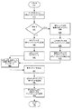
図3は、周辺インターフェイス回路の一実施形態のブロック図である。周辺インターフェイス回路350は、ダウンストリーム部360およびアップストリーム部450を含む。周辺インターフェイス回路350はさらに、図2のI/Oトンネル140のようなI/Oトンネルに接続されうるトンネル・インターフェイス・ロジックユニット355を含む。図3のダウンストリーム部360では、トンネル・インターフェイス・ロジック355はさらにコマンドバッファ370に結合される。コマンドバッファ370はタグ付けロジックユニット380に結合される。タグ付けロジックユニット380は仮想チャネルコマンドバッファ390に結合される。仮想チャネルコマンドバッファ390はアービトレーションロジックユニット410に結合される。アービトレーションロジックユニット410はバスインターフェイス回路470に結合されている。仮想チャネルコマンドバッファ390はさらに非ポスト(non-posted, NP)リトライキュー420および分割応答(split response)キュー430に結合されている。トンネル・インターフェイス・ロジック355はさらにデータバッファ400に結合され、データバッファ400は次にバスインターフェイス回路470に結合されている。バスインターフェイス回路470は周辺バス560に結合され、周辺バス560は周辺装置565に結合されている。
FIG. 3 is a block diagram of one embodiment of a peripheral interface circuit. Peripheral interface circuit 350 includes a downstream unit 360 and an upstream unit 450. Peripheral interface circuit 350 further includes a tunnel interface logic unit 355 that may be connected to an I / O tunnel, such as I / O tunnel 140 of FIG. In the downstream section 360 of FIG. 3, the tunnel interface logic 355 is further coupled to a command buffer 370. Command buffer 370 is coupled to tagging logic unit 380. Tagging logic unit 380 is coupled to virtual channel command buffer 390. Virtual channel command buffer 390 is coupled to
アップストリーム部450では、バスインターフェイス回路470が、NPコマンドバッファ480、解析ロジックユニット500および遅延トランザクションロジック回路510に結合される。さらに、バスインターフェイス回路470がデータバッファ550に結合される。NPコマンドバッファ480は、制御コマンドジェネレータ520およびNPソースタグ付けロジックユニット490に結合される。制御コマンドジェネレータ520は、仮想チャネルコマンドバッファ530およびトンネル・インターフェイス・ロジック355に結合されている。仮想チャネルコマンドバッファ530はトンネル・インターフェイス・ロジック355に結合されている。周辺インターフェイス回路350はさらに制御ロジックおよび記憶ユニット460を含み、制御ロジックおよび記憶ユニット460はダウンストリーム部360の分割応答キュー430およびデータバッファ400に結合されている。制御ロジックおよび記憶ユニット460はさらにアップストリーム部450のNPソースタグ付けロジックユニット490およびNPコマンドバッファ480に結合されている。さらに、周辺インターフェイス回路350は繰り返しロジック570を含み、これらは周辺バス580などの周辺バスに関して上述したように動作することが理解できるであろう。
In upstream section 450, bus interface circuit 470 is coupled to NP command buffer 480,
一般的に、「仮想チャネル」は様々な処理ノードの間でパケットを運ぶための通信路である。各仮想チャネルは他の仮想チャネルのリソースからは独立している(つまり、一つの仮想チャネルを流れるパケットは一般的に、物理的伝送の観点から、他の仮想チャネルにおけるパケットの存在の有無による影響を受けない。パケットは、パケットのタイプに基づいて仮想チャネルの割り当てを受ける。同じ仮想チャネルのパケットは、その他の送信と物理的に衝突する(同じ仮想チャネル内のパケットはリソースの衝突を生じさせる)が、異なった仮想チャネル内のパケット送信とは物理的に衝突しない。 In general, a “virtual channel” is a communication path for carrying packets between various processing nodes. Each virtual channel is independent of the resources of other virtual channels (ie, packets flowing through one virtual channel are generally affected by the presence or absence of packets in the other virtual channel from the perspective of physical transmission. Packets are assigned a virtual channel based on the type of packet, packets in the same virtual channel physically collide with other transmissions (packets in the same virtual channel cause resource collisions) ) Does not physically collide with packet transmissions in different virtual channels.
あるパケットは他のパケットと論理的に衝突する(つまり、プロトコルの理由、コヒーレンシーの理由、またはその他の似たような理由から、一のパケットが他のパケットと論理的に衝突しうる)。もし第1のパケットが論理的/プロトコルの理由からその宛先のノードに、第2のパケットがその宛先のノードに到達する前に、到達していなければならないとすると、もし第2のパケットが物理的に第1のパケットの伝送をブロックしていると(競合するリソースを占有することによって)コンピュータシステムはデッドロックになりうる。第1および第2のパケットを分離した仮想チャネルに割り当て、パケットのようなコンピュータシステム内の伝送媒体をお互いの伝送をブロックできない分離した仮想チャネルに割り当てることによって、デッドロックなしの動作が達成できる。異なった仮想チャネルからのパケットは同じ物理リンク上を伝送されることに注意してもらいたい。しかしながら、伝送の前に受信バッファを利用することが可能なので、この共有リソースを使用していても、仮想チャネルは互いをブロックしない。 Some packets logically collide with other packets (ie, one packet can logically collide with other packets for protocol reasons, coherency reasons, or other similar reasons). If the first packet must arrive at the destination node for logical / protocol reasons and the second packet must arrive before it reaches the destination node, then the second packet In particular, blocking the transmission of the first packet (by occupying competing resources) can cause the computer system to deadlock. By assigning the first and second packets to separate virtual channels and assigning transmission media in the computer system such as packets to separate virtual channels that cannot block each other's transmission, an operation without deadlock can be achieved. Note that packets from different virtual channels are transmitted on the same physical link. However, since the receive buffer can be used before transmission, the virtual channels do not block each other even if this shared resource is used.
一つの観点からは、異なったそれぞれのパケットタイプ(例えば、異なったコマンド符号化方式のそれぞれ)にそれ自身の仮想チャネルを割り当てることができ、それによって本実施形態では、分離したバッファが各仮想チャネルに割り当てられる。各仮想チャネルに対して分離したバッファを使用することができるので、ある仮想チャネルからのパケットは他の仮想チャネルからのパケットとは物理的に衝突しない(そのようなパケットは他のバッファに格納される)。 From one point of view, it is possible to assign its own virtual channel to each different packet type (eg, each of the different command encoding schemes), so that in this embodiment, a separate buffer is used for each virtual channel. Assigned to. Because a separate buffer can be used for each virtual channel, packets from one virtual channel do not physically collide with packets from other virtual channels (such packets are stored in other buffers). )
従って、図示した実施形態では、仮想チャネルコマンドバッファ390および仮想チャネルコマンドバッファ530はそれぞれ3つの分離したFIFO部を有し、それらは3つのタイプのトランザクション、ポスト(posted)、非ポスト(non-posted)および応答(response)に対応する。コマンドは、それらが受信された順番に、各FIFOに格納される。しかしながら、元のコマンドを生成した装置のタイプまたはバスに関する順序づけ規則を保持するために、異なったタイプのトランザクションの間で順番に関係なくトランザクションを処理しなければならない。 Thus, in the illustrated embodiment, the virtual channel command buffer 390 and the virtual channel command buffer 530 each have three separate FIFO sections, which are the three types of transactions, posted and non-posted. ) And response. Commands are stored in each FIFO in the order in which they are received. However, transactions must be processed out of order between the different types of transactions in order to preserve the ordering rules for the type of device or bus that generated the original command.
ある実施形態では、コマンドバッファ370は深さ2(2-deep)のFIFOであって、図2のI/Oトンネル140から図3の仮想チャネルコマンドバッファ390に送られたコマンドのバッファリング機構として機能する。トランザクションが周辺インターフェイス回路350に対してダウンストリームに送られるとき、トランザクションのデータ部分はデータバッファ400に記憶され、トランザクションのコマンド部分は仮想チャネルコマンドバッファ390に記憶される。しかしながら、まずタグ付けロジック380がコマンドに対してタグ値を生成し、それを付加するように構成されている。タグ値は、あるコマンドの、他の受信したコマンドに対する相対的な受信の順番に対応し、後続の調停サイクルで使用される。データおよびコマンドは、パケットに含まれるヘッダ情報によって同じパケットに属するものとして特定可能である。また、ある種の周辺バスはI/Oノードの内部クロック速度よりも遅いクロック速度で動作するので、データはI/Oノードのクロック速度を用いてデータバッファ400にロードされ、異なったクロック速度、好適にはバスインターフェイス回路470に接続された周辺バスのクロック速度でアンロードされる。さらに、データバッファ400および仮想チャネルコマンドバッファ390は、スペースが利用できないときには、そのことを任意のアップストリームロジックに通知するように構成できる。 In one embodiment, the command buffer 370 is a 2-deep FIFO, as a buffering mechanism for commands sent from the I / O tunnel 140 of FIG. 2 to the virtual channel command buffer 390 of FIG. Function. When a transaction is sent downstream to the peripheral interface circuit 350, the data portion of the transaction is stored in the data buffer 400 and the command portion of the transaction is stored in the virtual channel command buffer 390. However, the tagging logic 380 is first configured to generate a tag value for the command and append it. The tag value corresponds to the order of reception of a command relative to other received commands and is used in subsequent arbitration cycles. Data and commands can be specified as belonging to the same packet by header information included in the packet. Also, some peripheral buses operate at a clock speed that is slower than the internal clock speed of the I / O node, so data is loaded into the data buffer 400 using the clock speed of the I / O node, and a different clock speed, Preferably it is unloaded at the clock speed of the peripheral bus connected to the bus interface circuit 470. Further, the data buffer 400 and virtual channel command buffer 390 can be configured to notify any upstream logic when space is not available.
コマンドのタイプ(つまり、ポスト、非ポストまたは応答)に応じて、コマンドは、仮想チャネルコマンドバッファ390の各仮想チャネルFIFOに記憶される。アービトレーションロジック410は、仮想チャネルコマンドバッファ390内のトランザクションの間で、第1に処理するトランザクション、第2に処理するトランザクション(以下同様)を調停するように構成されている。仮想チャネルコマンドバッファ390およびアービトレーションロジック410は、それらが共同してコマンドが処理される順番を決定し記憶するので、コマンドスケジューラーと考えられる。例えば、非ポストコマンドの前に仮想チャネルコマンドバッファ390に到着したポストコマンドは、アービトレーションロジック410によって確立された順序づけ規則に従って、非ポストコマンドの後に処理しなければならない可能性がある。アービトレーションロジック410はさらに、アービトレーションサイクルの間、タグ付けロジックユニット380によって割り当てられたタグ値を使用することができる。
Depending on the type of command (ie, post, non-post or response), the command is stored in each virtual channel FIFO in the virtual channel command buffer 390. The
さらに、複数の応答パケットが同じデータストリームまたはシーケンスに属することがある。これは、データストリームに対する要求のような共通の要求トランザクションからそれらが由来している場合である。周辺バスによっては、ダウンストリームロジックで順番がバラバラにパケットが受信されたときであっても、データストリーム内では正しい順番で応答パケットを届ける必要がある。さらに、データストリームの要求に応答して、周辺バス上で部分的な転送を実行しなければならない。データバッファ400は、要求されたデータストリームの一部を形成するデータを含んでいてもよい。この一部を形成するデータセグメントが正しい順番であるかぎり、それらを周辺バスに転送することができる。 Furthermore, multiple response packets may belong to the same data stream or sequence. This is the case when they come from a common request transaction, such as a request for a data stream. Depending on the peripheral bus, even when packets are received out of order by the downstream logic, it is necessary to deliver response packets in the correct order in the data stream. In addition, partial transfers must be performed on the peripheral bus in response to a request for a data stream. Data buffer 400 may contain data that forms part of the requested data stream. As long as the data segments that form this part are in the correct order, they can be transferred to the peripheral bus.
制御ロジックおよび記憶ユニット460は、レジスタやランダムアクセスメモリなどの記憶ユニットと、データを供給するのに用いられるロジックとを含み、図7の説明と併せて、以下で詳しく説明する。
The control logic and
図8および図9に関係して、以下で詳細に説明するように、調停の間、もし勝ったトランザクションが応答コマンドであった場合、この応答コマンドに関係するデータがデータバッファ400にあるかどうかを判定する。もしデータがあるならば、周辺バス560上でバスサイクルを起動する。これは、コマンドおよびデータパケットを受信したバスインターフェイス回路470が、それらを周辺バス560上での伝送に適したアドレス、データおよび制御信号に変換することによって実行される。 As will be described in detail below in connection with FIGS. 8 and 9, if the transaction that won during the arbitration was a response command, whether the data associated with this response command is in the data buffer 400 Determine. If there is data, a bus cycle is started on the peripheral bus 560. This is performed by the bus interface circuit 470 receiving the command and data packets by converting them into address, data and control signals suitable for transmission on the peripheral bus 560.
もし勝利を獲得したコマンドがリードまたはライトのような非ポストコマンドであるならば、バスインターフェイス回路470に接続された周辺バスのタイプに応じて、周辺装置565は、例えば次のうちの一つを実行する:コマンドの受け入れおよび処理およびすべての要求されたデータとともにターゲット完了(done)サイクルまたは応答サイクルを送信する、リトライ指示をアサートする、コマンドの受け入れおよび分離応答指示をアサートする。図4の説明に関係して以下で詳細に説明するように、もしリトライ指示が周辺装置565によってアサートされると、非ポストコマンドを仮想チャネルコマンドバッファ390から回収して、NPリトライキュー420に記憶することができる。図5の説明に関係して以下で詳細に説明するように、もし周辺バス560がPCI−Xバスであり、分離応答が受信されると、非ポストコマンドを仮想チャネルコマンドバッファ390またはNPリトライキュー420から回収して、分割応答キュー430に記憶することができる。
If the winning command is a non-post command such as a read or write, depending on the type of peripheral bus connected to the bus interface circuit 470, the
アップストリーム部450では、周辺装置565が周辺バス560上でバスサイクルを起動するとき、バスインターフェイス回路470はそのサイクルを、上述したようにコマンドおよびデータパケットを含むパケットトランザクションに変換することができる。データパケットはデータバッファ550に記憶することができ、コマンドは仮想チャネルコマンドバッファ530の各仮想チャネルに記憶することができる。仮想チャネルコマンドバッファ530への記憶の前に、コマンドのタイプに応じて、解析ロジック500がコマンドをいくつかのより小さなコマンドに分解する。例えば、もし周辺装置565が、システムメモリに対する大きなデータブロックの非ポスト・ライトを要求したとすると、解析ロジック500は、メモリの同じブロックについての、より小さなブロック単位のいくつかの非ポスト・ライトコマンドを生成する。一実施形態としては、このブロックをキャッシュラインの境界に沿って生成できることが考えられる。続いて、非ポスト・コマンドのそれぞれを仮想チャネルコマンドバッファ530に記憶することができる。非ポスト・リードコマンドも、要求の境界およびトランザクションがPCIであるか、またはPCI−Xであるかに応じて、分解することができる。一実施形態では、NPソースタグ付けロジック490は、ダウンストリームロジックが特定の応答コマンドが関係するデータストリームを決定するのに用いることができる、タグ値を生成することができる。さらに、図6から図9に関係して以下で詳細に説明するように、元々の非ポスト・コマンド(例えば、分解される前)をNPコマンドバッファ480に保持してダウンストリーム部360内のロジックに情報を供給することができる。NPソースタグ付けロジック490は、アップストリームの非ポスト・コマンドに関するタグ値を生成することができる。一実施形態では、0から29までのタグ値が生成される。しかしながら、他の実施形態では、他の適切な数のタグ値を生成することが可能であると考えられる。
In the upstream unit 450, when the
アップストリームコマンドが仮想チャネルコマンドバッファ530内に記憶されると、制御コマンドジェネレータ520が、図2のトランシーバ110および120によって生成される制御コマンドに類似した制御コマンドを生成する。図3で、制御コマンドジェネレータ520はさらに、これらの制御コマンドを、トンネル・インターフェイス・ロジック355を通じて図2のトンネル制御ユニット130に送ることができ、それによってアップストリームコマンドをI/Oトンネル140のスケジュールに入れることができる。図3のトンネル・インターフェイス・ロジック355は、I/Oトンネル140と周辺インターフェイス回路350内のロジックとの間のインターフェイスを提供するのに必要な汎用のバッファ回路を含んでいてもよい。
As upstream commands are stored in virtual channel command buffer 530, control command generator 520 generates a control command similar to the control command generated by
遅延トランザクションロジック510は、バスインターフェイス回路470、ダウンストリーム部360内のロジックおよび図2のI/Oトンネルロジックとの組み合わせで動作する回路を含み、要求をただちに処理することができない周辺装置565に対してリトライ指示を送る。例えば、周辺装置565が非ポスト・リード要求をアップストリームに送り、そして非ポストチャネルはブロックされているか、またはデータの準備ができていないとする。遅延トランザクションロジック510は周辺装置565に対して、その要求を現在処理することができないこと、および後でその要求をリトライすべきことを指示することができる。
The delayed transaction logic 510 includes a circuit that operates in combination with the bus interface circuit 470, the logic in the downstream section 360, and the I / O tunnel logic of FIG. Send a retry instruction. For example, assume that peripheral 565 sends a non-post read request upstream and the non-post channel is blocked or not ready for data. The deferred transaction logic 510 can instruct the
図4は、非ポスト・リトライバッファ回路の一実施形態のブロック図である。非ポスト(NP)リトライバッファ回路650は、非ポストコマンドアップデート回路670に結合された非ポストリトライFIFO660を含む。
図示された実施形態では、非ポストリトライFIFO660は、図3の仮想チャネルコマンドバッファ回路390の非ポストコマンドFIFOのような、非ポストコマンドバッファから受信した非ポストコマンドを記憶することができる。図3の説明に関係して上述したように、周辺装置565によってアサートされたリトライ指示に応答して、非ポストコマンドを仮想チャネルコマンドバッファ390から回収して、図4の非ポストリトライFIFO660に記憶することができる。
FIG. 4 is a block diagram of one embodiment of a non-post retry buffer circuit. Non-post (NP) retry
In the illustrated embodiment, the non-post-retry FIFO 660 can store non-post commands received from a non-post command buffer, such as the non-post command FIFO of the virtual channel command buffer circuit 390 of FIG. As described above in connection with the description of FIG. 3, in response to the retry instruction asserted by
非ポストリトライFIFO660は、利用可能な記憶位置がない場合には、FIFOフル(full)信号をアサートする。このフル信号は、図3のアービトレーションロジック回路410のようなアービトレーションロジックに対して指示を与える。フル信号がアサートされている間は、仮想チャネルコマンドバッファ回路390の非ポストコマンドFIFOは調停サイクルに参加することはできず、それによって追加のリトライ指示が発生した際の非ポストリトライFIFO660のオーバーフローを防止する。
The non-post-retry FIFO 660 asserts a FIFO full signal when no storage location is available. This full signal provides an indication to arbitration logic, such as the
ひとたび非ポストコマンドが非ポストリトライFIFO660に記憶されると、非ポストリトライFIFO660の先頭のコマンドが、図3の仮想チャネルコマンドバッファ回路390のどれかの仮想に記憶された任意のコマンドとともに、調停サイクルに参加することができる。もし、図4の非ポストリトライFIFO660の先頭に記憶された非ポストコマンドが調停サイクル中に選択されてバスサイクルを起動させるとき、そしてリトライ信号が図3の周辺バス560再度アサートされるとき、図4の非ポストコマンドアップデート回路670が選択された非ポストコマンドを非ポストリトライFIFO660の先頭から取り除いて、その末尾に記憶し、それが再度当該FIFOの先頭に到達する別の調停サイクルまで待機する。言い換えれば、この選択された非ポストコマンドはFIFOに書き戻される。このことが、非ポストコマンドアップデート回路670内の点線矢印で表されている。このサイクルの再試行(リトライ)は何回でも発生し、毎回コマンドが非ポストリトライFIFO660の末尾に書き戻される。
Once a non-post command has been stored in the non-post-retry FIFO 660, the top command of the non-post-retry FIFO 660, along with any virtually stored command in any of the virtual channel command buffer circuits 390 of FIG. Can participate in. If the non-post command stored at the beginning of the non-post-retry FIFO 660 of FIG. 4 is selected during the arbitration cycle to initiate a bus cycle, and the retry signal is reasserted by the peripheral bus 560 of FIG. 4 non-post
図3の周辺インターフェイス回路350がPCIモードで動作しているとき、図3の周辺バス560が、非ポストサイクルが部分的に完了したことを示すことがある。例えば、非ポスト・リードコマンドが10個のデータセグメントを要求したとする。周辺装置565はリトライ指示をアサートするが、10個のデータセグメントのうち5個で応答し、それによって応答の部分的な完了を示すことができる。部分的完了の表示を受信すると、図4の非ポスト・コマンドアップデート回路670は非ポストコマンドを修正して、残りのデータセグメントに対応した新しいデータ数およびアドレスが保存されるようにする。同様に、非ポスト・ライトコマンドも部分的に完了することがある。次に、非ポストコマンドアップデート回路670は修正された非ポストコマンドを非ポストリトライFIFO660の末尾に記憶させ、その非ポストコマンドはそれが再度当該FIFOの先頭に到達する別の調停サイクルまで待機する。ここでの用法として、例示の目的において、FIFOの先頭とはコマンドがアンロードされる、つまり読み出されるFIFO内の位置を意味し、FIFOの末尾とはコマンドがストアされ、つまり書き込まれる位置を意味する。さらに、非ポストリトライFIFO660からコマンドがアンロードされるにつれ、非ポストリトライFIFO660内に記憶されたすべてのコマンドはそれが将来アンロードされる順番に持ち上がることが理解できる。別の実施形態としては、コマンドをFIFOの先頭に書き込み、FIFOの末尾から読み出すことが考えられる。この場合、非ポスト・コマンドアップデート回路670はFIFOの先頭にコマンドを書き込む。
When peripheral interface circuit 350 of FIG. 3 is operating in PCI mode, peripheral bus 560 of FIG. 3 may indicate that the non-post cycle has been partially completed. For example, suppose a non-post-read command requested 10 data segments.
図5に、周辺インターフェイス回路の一実施形態におけるスリット応答指示(slit response indication)の取り扱いを示す流れ図を示す。図3および図5をまとめて参照して、処理は図5のステップ431から始まり、ステップ432に進む。ステップ432では、非ポストコマンドが図3のダウンストリーム部450で受信され、仮想チャネルコマンドバッファ390の非ポストFIFOに記憶される。図5のステップ433に進んで、調停サイクルが実行され、もし非ポストコマンドが勝った場合には処理はステップ434へと進み、そうでない場合には非ポストコマンドが勝つまで調停サイクルが継続する。従って、ステップ434へと進み、非ポストコマンドが選択され、例えば図3のバスインターフェイス回路470に含まれる変換ロジックに送られる。この非ポストコマンドは対応するバスサイクルにおいて周辺バス560上での伝送に適するように変形される。図5のステップ435に進んで、次に図3のバスインターフェイス回路470によってバスサイクルが開始される。これらの変換およびバスサイクルの開始プロセスは、図2の説明に関して上述したCREXインターフェイス(図示せず)などの周辺バスに対する一以上のインターフェイスによって実行される一以上の中間のステップを含んでいてもよいことを理解してもらいたい。次に処理は図5のステップ436へ進む。ステップ435では、図3のアップストリーム部450およびバスインターフェイス回路470が、周辺バス560上の周辺装置565などの目的装置からの完了表示を待つ。もし非ポストコマンドがリード要求であったときは、完了表示は、すべての要求されたデータが存在していることを示す、「サイクル完了」信号のような制御信号を含む、要求されたすべてのデータである。もし非ポストコマンドがライト要求であったときは、完了表示は、データを伴わない完了のメッセージである。完了表示を受信すると、処理は図5のステップ437へと進む。ステップ437では、非ポストコマンドがライトコマンドであったときは、図3のアップストリーム部450が「目標完了」応答などの応答コマンドを、要求しているノードに対して送る。もし、非ポストコマンドがリードコマンドであったときは、アップストリーム部450は要求しているノードに、要求されたすべてのデータを含む応答コマンドを転送する。処理説明は図5のステップ438で終了する。
FIG. 5 is a flow diagram illustrating the handling of slit response indication in one embodiment of the peripheral interface circuit. With reference to FIGS. 3 and 5 collectively, the process starts at step 431 in FIG. 5 and proceeds to step 432. In step 432, the non-post command is received by the downstream unit 450 of FIG. 3 and stored in the non-post FIFO of the virtual channel command buffer 390. Proceeding to step 433 of FIG. 5, an arbitration cycle is performed, and if the non-post command wins, the process proceeds to step 434, otherwise the arbitration cycle continues until the non-post command wins. Thus, proceeding to step 434, a non-post command is selected and sent to the conversion logic included in the bus interface circuit 470 of FIG. 3, for example. This non-post command is modified to be suitable for transmission on the peripheral bus 560 in the corresponding bus cycle. Proceeding to step 435 of FIG. 5, the bus interface circuit 470 of FIG. These conversion and bus cycle initiation processes may include one or more intermediate steps performed by one or more interfaces to a peripheral bus, such as the CREX interface (not shown) described above with respect to the description of FIG. I want you to understand that. Next, the process proceeds to step 436 in FIG. In step 435, the upstream unit 450 and the bus interface circuit 470 of FIG. 3 wait for a completion display from the target device such as the
ステップ436に戻って、図3の周辺バス560から受信した応答が完了メッセージでない場合、それは図4との関係で詳細に説明したリトライ表示である可能性がある。応答は分割応答表示であってもよく、図5のステップ439で分割応答表示が受信される。ステップ440に進んで、分割応答表示に応答して、非ポストコマンドが図3の分割応答キュー430に記憶される。非ポストコマンドは、バス番号、デバイス番号、関数番号、カウントおよびID番号などのバスサイクル情報を含みうる。この情報は、目的の装置(デバイス)から受信した任意の応答サイクルを獲得するのに用いることができる。図5のステップ441に進んで、もし非ポストコマンドがリードコマンドであったときは、受信された分割応答はリードされたデータを伴う。この場合、応答コマンドは任意の利用可能なデータとともに要求しているノードに送られる。ステップ442に進んで、もし分割完了が受信されると、それは非ポスト・ライトコマンドに応答する分割完了メッセージであるか、要求されたすべてのデータを含む分割完了である。ステップ443に進んで、分割完了サイクル情報が図3の分割応答キュー430内に記憶された任意の非ポストコマンドと比較される。対応する非ポストコマンドが決定されると、処理は図5のステップ444へと進む。ステップ444では、もし分割完了が分割完了メッセージであるときは、「目標完了」応答などの応答コマンドが要求しているノードに送られる。もし非ポストコマンドがリードコマンドであるならば、図3のアップストリーム部450は要求されたすべてのデータを含む応答コマンドを要求しているノードに送信することができる。図5のステップ445に進んで、すべてのデータまたは分割完了メッセージが受信されると、対応する非ポストコマンドが図3の分割応答キュー430から回収される。
Returning to step 436, if the response received from the peripheral bus 560 of FIG. 3 is not a completion message, it may be a retry indication described in detail in relation to FIG. The response may be a split response display, and the split response display is received at step 439 of FIG. Proceeding to step 440, in response to the split response indication, the non-posted command is stored in the split response queue 430 of FIG. The non-post command may include bus cycle information such as a bus number, device number, function number, count, and ID number. This information can be used to acquire any response cycle received from the target device. Proceeding to step 441 in FIG. 5, if the non-post command is a read command, the received split response is accompanied by the read data. In this case, the response command is sent to the requesting node along with any available data. Proceeding to step 442, if a split complete is received, it is a split complete message in response to a non-post-write command or a split complete including all requested data. Proceeding to step 443, the split completion cycle information is compared with any non-posted commands stored in the split response queue 430 of FIG. When the corresponding non-post command is determined, processing proceeds to step 444 in FIG. In
ステップ442に戻って、分割完了が受信されないときは、処理はステップ446に進み、分割応答が受信される。次に処理はステップ447に進み、分割応答サイクル情報が、図3の分割応答キュー430内に記憶されたすべての非ポストコマンドと比較される。対応する非ポストコマンドが決定されると、処理は図5のステップ448へ進む。ステップ448では、図3のアップストリーム部450が、利用可能なデータと非ポストコマンドからの情報を含む応答コマンドを要求しているノードに送信する。処理はステップ442へと戻り、他の応答を待つ。ステップ446へと戻って、分割応答が受信されないときは、処理はステップ442へと戻り、他の応答を待つ。 Returning to step 442, if a split completion is not received, processing proceeds to step 446 and a split response is received. Processing then proceeds to step 447 where the split response cycle information is compared with all non-post commands stored in the split response queue 430 of FIG. When the corresponding non-post command is determined, processing proceeds to step 448 of FIG. In step 448, the upstream unit 450 of FIG. 3 sends a response command including available data and information from the non-post command to the requesting node. Processing returns to step 442 to wait for another response. Returning to step 446, if a split response is not received, the process returns to step 442 to wait for another response.
図6は、バッファ利用可能性FIFO構造を含むバッファ回路の一実施形態のブロック図である。バッファ回路680は、非ポスト・コマンドバッファ690に結合されたバッファ利用可能性FIFO685を有する。バッファ利用可能性FIFO685はさらにライトロジック686およびリタイアロジック687に結合されている。
FIG. 6 is a block diagram of one embodiment of a buffer circuit including a buffer availability FIFO structure. Buffer circuit 680 has a buffer availability FIFO 685 coupled to
非ポストコマンドバッファ690は、図3の周辺バス560のような周辺バスから受信したコマンドに対応する非ポストコマンドを記憶する。図3の説明に関連して上述したように、アップストリームの非ポストコマンドは、そのアップストリームの非ポストコマンドに含まれている情報を必要とするダウンストリームの回路がそれを使用するために保持される。非ポスト・コマンドバッファ690にコマンドを記憶するのを促進するために、バッファ利用可能性FIFOは、非ポスト・コマンドバッファ690内の次の利用可能な位置を示すことができる。
非ポスト・コマンドバッファ690が空であるときは、非ポスト・コマンドバッファ690がいっぱいになるまで、コマンドをシーケンシャルに記憶することができる。非ポストコマンドに関係する応答の受信の順番に応じて、非ポストコマンドは除去され、または順番に関係なく回収される。これによって、調停パターンに「穴」または空き位置を残す。従って、非ポスト・コマンドバッファ690に任意の新しいコマンドを記憶するために、バッファ利用可能性FIFO685を用いて、利用可能な位置を追跡記録することができる。
When the
図示された実施形態では、非ポスト・コマンドバッファ690は8つの位置を含んでいる。バッファ利用可能性FIFO685も8つの位置を含み、バッファ利用可能性FIFO685内の8つの位置のそれぞれは3ビットの値を記憶することができる。バッファ利用可能性FIFO685に記憶された値は、非ポスト・コマンドバッファ690内の位置のアドレスに対応する。従って、3ビットの値のそれぞれは非ポストコマンドバッファ690に対するインデックスとして用いることができる。他の実施形態では、他の適切な位置の数および異なったビット数を採用することができる、ことが考えられる。バッファ利用可能性FIFO685はFIFO構造なので、値はそれらが書き込まれた順番で読み出される。従って、本実施形態では、値は、バッファ利用可能性FIFO685のボトム(末尾)に書き込まれ、そのトップ(先頭)から読み出されるといえる。しかしながら、他の実施形態においては、トップおよびボトムという用語は相互に使用可能であると考えられる。さらに、他の実施形態においては、バッファ利用可能性FIFO685内の各位置を示すのにリードおよびライトポインタを使用可能であることが考えられる。
In the illustrated embodiment, the
初期化時には、非ポストコマンドバッファ690は空であり、従ってすべての位置が利用可能である。バッファ利用可能性FIFO685は、バッファ利用可能性FIFO685のトップが非ポストコマンドバッファ690の位置0のアドレスに対応するインデックス値を含むように、初期化することができる。バッファ利用可能性FIFO685の次の位置は位置1、その他のアドレスに対応するインデックス値を含む。従って、非ポストコマンドが到着したとき、ライトロジック686はバッファ利用可能性FIFO685のトップに含まれているインデックス値を読み込み、その後、位置0のアドレスにコマンドを書き込む。コマンドが記憶されると、バッファ利用可能性FIFO685に記憶されていたすべてのインデックス値が位置ひとつ分だけ上方にシフト(シフトアップ)し、それによって位置1のアドレスはバッファ利用可能性FIFO685のトップ位置となる。
At initialization, the
特定のダウンストリームコマンドが完了して、非ポストコマンドバッファ690に記憶された対応する非ポストコマンドがこれ以上必要なくなったとき、それは非ポストコマンドバッファ690から回収されうる。従って、非ポスト・コマンドバッファ690は、非ポストコマンドが記憶されていた位置を利用可能にし、リタイアロジック687に対応する表示を供給する。リタイアロジック687は、その位置が利用可能になったときを決定でき、それに応答して、バッファ利用可能性FIFO685に対する利用可能な位置のアドレスに対応するインデックス値を、バッファ利用可能性FIFO685のボトムに書き込む。従って、バッファ利用可能性FIFO685のトップ位置は、利用可能な位置が存在するときに、利用可能な位置のアドレスに対応するインデックス値を含む。非ポスト・コマンドバッファ690に利用可能な位置がない場合には、ライトロジック686は非ポストコマンドバッファ690にどんなコマンドも記憶することを禁止される。
When a particular downstream command is complete and the corresponding non-post command stored in
図7に、図3の制御ロジックおよび記憶ユニットの一実施形態の典型的なダイアグラムを示す。制御ロジックおよび記憶ユニット460は、バッファ利用可能性レジスタ600、先頭レジスタ610、次ポインタレジスタ620、末尾レジスタ630および分割応答ポインタレジスタ640を含む。
FIG. 7 shows an exemplary diagram of one embodiment of the control logic and storage unit of FIG. The control logic and
図示された実施形態においては、先頭レジスタ610は29ビットを有し、それは図3のNPソース・タグ付けロジックユニット490によって生成された29の可能性のあるタグ値に対応する。先頭レジスタ610は、どのコマンドパケットが各データストリームの第1コマンドパケットであるのかを示すのに使用される。例えば、ビット0および3が、タグ値0と3を有するコマンドパケットが先頭パケットであることを示すためにセットされる。ここで、データストリームとは、データ要求に関連した一以上のパケットシーケンス中の任意の数のパケットを指す。例えば、非ポスト・リード要求コマンドは、同じデータストリームに属するいくつかのリードコマンドに分解することができる。2パケット以上を含むデータストリームについては、次ポインタ620および末尾レジスタ630を用いて、データストリーム中の残りのパケットの順番を追跡記録することができる。
In the illustrated embodiment, the leading register 610 has 29 bits, which corresponds to the 29 possible tag values generated by the NP source tagging logic unit 490 of FIG. The head register 610 is used to indicate which command packet is the first command packet of each data stream. For example,
次ポインタ620も29の位置を含む。それぞれの位置は、少なくとも29個のタグ値を表すために5ビットを記録することができる。従って、各位置は29個のタグ値の一つを表すことができる。従って、次ポインタ620の各位置に記憶された値は、次ポインタ620内の次の位置を示すために使用できる。さらに、各位置に記憶された値は、特定のデータストリーム内の次のパケットのタグ値をも表す。従って、次ポインタ620内に記憶された値のシーケンスは、送られた順番に受信されていない可能性のあるデータストリーム中の多くのパケットの順番を再構成または検証するために使用することができる。 The next pointer 620 also includes 29 positions. Each location can record 5 bits to represent at least 29 tag values. Thus, each position can represent one of 29 tag values. Thus, the value stored at each position of the next pointer 620 can be used to indicate the next position within the next pointer 620. In addition, the value stored at each location also represents the tag value of the next packet in the particular data stream. Thus, the sequence of values stored in the next pointer 620 can be used to reconstruct or verify the order of many packets in the data stream that may not have been received in the order they were sent. .
末尾レジスタ630もまた29ビットを含み、それぞれが29個のタグ値に対応する。末尾レジスタ630は、特定のデータストリーム中の最終パケットに対応するタグ値を表すのに使用することができる。図示された実施形態においては、ビット2および5がセットされて、タグ値0および3を有するコマンドパケットが末尾パケットであることを示す。
The tail register 630 also includes 29 bits, each corresponding to 29 tag values. The tail register 630 can be used to represent a tag value corresponding to the last packet in a particular data stream. In the illustrated embodiment,
上述の実施形態においては末尾レジスタを特定のデータストリーム中の最終パケットを識別するために用いているが、別の実施形態では、特別な値を次ポインタ620の位置に記憶することができると考えられる。この特別の値は、それが記憶されている位置に対応するタグ値が特定のデータストリーム中の最終パケットに対応することを示すことができる。 Although the tail register is used in the above embodiment to identify the last packet in a particular data stream, in another embodiment, a special value can be stored at the next pointer 620 location. It is done. This special value can indicate that the tag value corresponding to the location where it is stored corresponds to the last packet in a particular data stream.
図示された実施形態においては、バッファ利用可能性レジスタ600もまた29ビットを含み、それぞれが29個のタグ値に対応する。バッファ利用可能性レジスタ600は、特定のデータストリームに関連した応答のうちどれが受信されたかを示すのに使用できる。例えば、タグ値3および4を含むデータパケットが受信され、図3のデータバッファ400のようなデータバッファに記憶される。従って、図7のバッファ利用可能性レジスタ600のビット番号3および4を設定することで、データが利用可能であることを示す。
In the illustrated embodiment, the buffer availability register 600 also includes 29 bits, each corresponding to 29 tag values. The buffer availability register 600 can be used to indicate which of the responses associated with a particular data stream has been received. For example, a data packet including
分割応答ポインタ640もまた29個の位置を含み、それぞれが図3のNPコマンドバッファ480のようなバッファ中の最大8つの位置を表す3ビットを記憶することができる。3ビットの値のそれぞれは、図3のNPコマンドバッファ480中の位置のアドレスに対応するインデックス値として使用できる。従って、分割応答ポインタ640は、どの応答コマンドが図3のNPコマンドバッファ480中に記憶された元の非ポストコマンドに関連しているかを示すために使用可能である。従って、分割応答ポインタ640は、周辺バスへのデータの部分的な転送が必要であるときに、使用される。 Split response pointer 640 also includes 29 positions, each of which can store 3 bits representing up to 8 positions in a buffer, such as NP command buffer 480 of FIG. Each 3-bit value can be used as an index value corresponding to the address of the position in the NP command buffer 480 of FIG. Accordingly, split response pointer 640 can be used to indicate which response command is associated with the original non-post command stored in NP command buffer 480 of FIG. Accordingly, the split response pointer 640 is used when partial transfer of data to the peripheral bus is required.
これまで29個のタグ値があるものとして説明したが、他の実施形態では、より少ない個数またはより多い個数のタグ値の使用が考えられる、ことを理解してもらいたい。従って、先頭レジスタ610、次ポインタ620、末尾レジスタ630、バッファ利用可能性レジスタ600および分割応答ポインタ640はそれぞれ、より多いビット数またはより少ないビット数を含むものであってもよいと考えられる。さらに、これらのレジスタに関連するロジックは反転していてもよいと考えられる。つまり、対応するタグ値を表すためには、ビットをセットするのではなく、それをクリアするのである。 Although described so far as having 29 tag values, it should be understood that in other embodiments, fewer or more tag values may be used. Thus, it is contemplated that the start register 610, next pointer 620, end register 630, buffer availability register 600, and split response pointer 640 may each contain a greater or lesser number of bits. Furthermore, it is contemplated that the logic associated with these registers may be inverted. That is, instead of setting a bit to represent the corresponding tag value, clear it.
図3の説明に関連してすでに説明したように、バスインターフェイス回路470によってバスサイクルが非ポスト・パケットコマンドに変換されるとき、その非ポスト・パケットコマンドに関連するいくつかの応答パケットが存在しうる。さらに、応答パケットはダウンストリーム部360によって順序がバラバラに受信される可能性があること、そしてデータストリーム中のパケットの順序付けは周辺バスのタイプに応じて維持されうることに言及した。図8および図9の説明に関連して、以下でさらに詳しく説明するように、非ポストコマンドはアップストリーム部450で受信され、それら非ポストコマンドに対するソースタグ値はソースタグ付けロジックユニット490によって生成される。続いて、制御ロジックおよび記憶ユニット460内の先頭レジスタ610、次ポインタ620、末尾レジスタ630、バッファ利用可能性レジスタ600および分割応答ポインタ640は、非ポストソースタグ値を用いて、一以上のデータストリーム中の応答の正しい順番を維持するために用いることができる。さらに、応答が受信されたとき、制御ロジックおよび記憶ユニット460は、データストリームの一部を形成するデータシーケンスを転送するときに使用可能である。
As already described in connection with the description of FIG. 3, when a bus cycle is converted to a non-posted packet command by the bus interface circuit 470, there are several response packets associated with that non-posted packet command. sell. Furthermore, it has been mentioned that response packets may be received out of order by the downstream unit 360, and that the ordering of packets in the data stream may be maintained depending on the type of peripheral bus. As described in more detail below in connection with the description of FIGS. 8 and 9, non-post commands are received at upstream portion 450 and source tag values for those non-post commands are generated by source tagging logic unit 490. Is done. Subsequently, the start logic 610, the next pointer 620, the tail register 630, the buffer availability register 600, and the split response pointer 640 in the control logic and
図示された実施形態では、記憶装置(storage)としてレジスタを使用しているが、他の実施形態では、例えばランダム・アクセス・メモリまたは任意のタイプの消去可能プログラム可能なリードオンリーメモリなどの、他の適切なタイプの記憶装置を使用できると考えられることに注意してもらいたい。 In the illustrated embodiment, a register is used as storage, but in other embodiments, other such as random access memory or any type of erasable programmable read-only memory. Note that you can use any appropriate type of storage device.
図8は、図3の周辺インターフェイス回路350の一実施形態であるトランザクション並び替え(リオーダリング)処理を説明する流れ図である。図3、図7および図8をまとめて参照して、処理は図8のステップ800で始まり、ステップ810に進む。ステップ810では、非ポストコマンドが図3のアップストリーム部450によって受信される。図8のステップ820に進んで、図3の解析ロジック500が、アップストリームI/Oトンネル要求を満たすために、非ポストコマンドを複数の非ポストコマンドに分解するかどうかを決定する。もし、トランザクションがPCIトランザクションまたはPCI−Xトランザクションであって、非ポストコマンドを分解する必要がないときは、処理は図8のステップ830に進んで、非ポストコマンドが図3のNPコマンドバッファ480に記憶される。一般的に、PCIトランザクションは分解されない。例えば、図3の周辺インターフェイス回路350による非ポスト・リード要求は最大でキャッシュラインの境界までのものである。しかしながら、PCIトランザクションは、決してある特定の場合に分解されることから除外されるものではない。
FIG. 8 is a flowchart illustrating a transaction rearrangement process that is one embodiment of the peripheral interface circuit 350 of FIG. With reference to FIGS. 3, 7, and 8 collectively, the process begins at
図8のステップ840に処理を進めて、非ポスト・ソースタグ値が生成され、その非ポストコマンドに付加される。処理はステップ842に進んで、非ポストコマンドのためにちょうど生成されたソースタグ値に対応するビットをセットすることによって、図7の先頭レジスタ610がアップデート(更新)される。処理は図8のステップ850に進んで、図3の制御コマンドジェネレータ520によって非ポストコマンドのために制御コマンドが生成され、調停のためにI/Oトンネル制御ロジックに送られる。図8のステップ860へ進んで、非ポストコマンドがさらに図3の仮想チャネルコマンドバッファ530内に記憶されて送信を待つ。図8のステップ870で、もし対応する制御コマンドがI/Oトンネル制御ロジック内のアービトレーション回路によって選択されたならば、非ポストコマンドが送信される。
Proceeding to step 840 of FIG. 8, a non-post source tag value is generated and appended to the non-post command. Processing proceeds to step 842 where the first register 610 of FIG. 7 is updated by setting the bit corresponding to the source tag value just generated for the non-post command. Processing proceeds to step 850 of FIG. 8 where a control command is generated for a non-post command by control command generator 520 of FIG. 3 and sent to the I / O tunnel control logic for arbitration. Proceeding to step 860 of FIG. 8, non-post commands are further stored in virtual channel command buffer 530 of FIG. 3 to wait for transmission. In
図8のステップ820に戻って、もし非ポストコマンドの分析が必要ならば、処理はステップ825へと進んで、非ポストコマンドは、同じシーケンスまたはデータストリームに属する複数の非ポストコマンドに分解される。ステップ835に進んで、元々の非ポストコマンドが、図3のNPコマンドバッファ480に記憶される。図8のステップ845において、元々の非ポストコマンドから作成されたばかりの複数の非ポストコマンドそれぞれに対して、NPソースタグが生成される。処理はステップ842へと進んで、図7の先頭レジスタ610、次ポインタ620、末尾レジスタ630および分割応答ポインタ640がアップデートされる。先頭レジスタ610は、シーケンス内の第1非ポストコマンドについて生成されたばかりのタグ値に対応するビットをセットすることでアップデートされる。末尾レジスタ630は、データストリーム内の最終非ポストコマンドについて生成されたばかりのタグ値に対応するビットをセットすることでアップデートされる。 Returning to step 820 of FIG. 8, if analysis of non-post commands is required, processing proceeds to step 825 where the non-post commands are broken down into multiple non-post commands belonging to the same sequence or data stream. . Proceeding to step 835, the original non-post command is stored in the NP command buffer 480 of FIG. In step 845 of FIG. 8, an NP source tag is generated for each of a plurality of non-post commands just created from the original non-post command. The process proceeds to step 842, where the top register 610, the next pointer 620, the end register 630, and the division response pointer 640 in FIG. 7 are updated. The leading register 610 is updated by setting the bit corresponding to the tag value just generated for the first non-post command in the sequence. The tail register 630 is updated by setting the bit corresponding to the tag value just generated for the last non-post command in the data stream.
次ポインタ620は、シーケンス内の残りの非ポストコマンドのタグ値をロードすることでアップデートされる。このタグ値は、シーケンス内の各パケットをそのシーケンス内の次のパケットにリンクするようにロードされる。例えば、与えられたデータストリームが3つのパケットから構成されているとする。このパケットは0、1、2として配置され、従って0、1、2とタグ付けされる。従って、先頭レジスタ610のビット0がセットされ、ビット1および2はクリアされる。その理由は、1つのパケットのみが先頭になれるからである。このデータストリーム中の次のパケットを追跡するために、次ポインタ620の位置0および1が、次の2つのパケットのタグ値、それぞれ1および2とともにロードされる。先頭レジスタ610のビット0がセットされているので、次ポインタ620の位置0がタグ値「1」とともにロードされ、タグ値1を持つパケットがデータストリーム中の「次の」パケットであることを示す。さらに、次ポインタ620の位置1がタグ値「2」とともにロードされ、タグ値2を持つパケットがデータストリーム中の「次の」パケットであることを示す。パケット2はデータストリーム中の最終のパケットであるので、それは末尾であると指定される。したがって、末尾レジスタ630のビット2がセットされる。上述の実施形態では、タグ値には数字のシーケンス(例えば、0,1,2)が割り当てられているものの、他の実施形態においてはタグ値に任意の順序を割り当てることができ、そして現在どのタグ値が利用可能であるのかに従ってタグ値を割り当てることが考えられる、ことを理解してもらいたい。さらに、他の実施形態では、データストリーム中により多くのまたはより少ない数のパケットを含むことができ、それによってより多くのまたはより少ないタグ値が用いられる。
The next pointer 620 is updated by loading the tag values of the remaining non-post commands in the sequence. This tag value is loaded to link each packet in the sequence to the next packet in the sequence. For example, assume that a given data stream is composed of three packets. This packet is arranged as 0, 1, 2 and is therefore tagged as 0, 1, 2. Therefore,
データストリームを構成する複数の非ポストコマンドがダウンストリームロジックによって順序がバラバラに受信され、それらを要求している装置に送るのに遅延が生じる可能性がある。この遅延は図3の周辺インターフェイス回路350にPCI−Xトランザクションに対する分割応答を指示させる。このような場合、ダウンストリームロジックは多くの分割応答サイクルおよび分割完了サイクルの発信元となり、そして複数の非ポストコマンドに対応する元々の非ポストコマンドに含まれている情報が分割応答および完了バスサイクルを開始するために必要である。図9に関連して以下でさらに詳細に説明するように、図7の分割応答ポインタレジスタ640は、特定のデータストリームの複数の応答それぞれを、図3のNPコマンドバッファ480に記憶されている元々の非ポストコマンドにリンクするために用いることができる。従って、図7の分割応答ポインタレジスタ640の各位置は、対応する応答コマンドのNPソースタグ値を表す。各位置は、その応答に対する元々の非ポストコマンドが記憶されている、図3のNPコマンドバッファ480内の位置のアドレスに対応するインデックス値とともにロードされる。上の例では、図7の分割応答ポインタレジスタ640中の位置0、1および2は、元々の非ポストコマンドが記憶されている、図3のNPコマンドバッファ480内の位置のアドレスに対応するインデックス値とともにロードされる。 Multiple non-post commands that make up the data stream are received out of order by the downstream logic, and there may be a delay in sending them to the requesting device. This delay causes the peripheral interface circuit 350 of FIG. 3 to instruct a split response to the PCI-X transaction. In such cases, the downstream logic is the source of many split response cycles and split completion cycles, and the information contained in the original non-post command corresponding to multiple non-post commands is split response and completion bus cycles. Is needed to start. As will be described in more detail below with respect to FIG. 9, the split response pointer register 640 of FIG. 7 originally stores each of a plurality of responses for a particular data stream in the NP command buffer 480 of FIG. Can be used to link to non-post commands. Accordingly, each position of the split response pointer register 640 in FIG. 7 represents the NP source tag value of the corresponding response command. Each position is loaded with an index value corresponding to the address of the position in the NP command buffer 480 of FIG. 3 where the original non-post command for that response is stored. In the above example, positions 0, 1 and 2 in the split response pointer register 640 of FIG. 7 are indices corresponding to the addresses of the positions in the NP command buffer 480 of FIG. 3 where the original non-post command is stored. Loaded with value.
処理は次に図8のステップ850に進み、複数の非ポストコマンドのそれぞれに対する制御コマンドが生成され、I/Oトンネル制御ロジックに送られる。さらに、ステップ860において、複数の非ポストコマンドのそれぞれが図3の仮想チャネルコマンドバッファ530内に記憶され、送信を待つ。図8のステップ870へと進み、I/Oトンネル制御ロジック内で調停回路によって、対応する各制御コマンドが選択されるとき、複数の非ポストコマンドのそれぞれが送信される。処理の説明は、ステップ880で終了する。 Processing then proceeds to step 850 of FIG. 8 where a control command for each of the plurality of non-post commands is generated and sent to the I / O tunnel control logic. Further, at step 860, each of the plurality of non-post commands is stored in the virtual channel command buffer 530 of FIG. 3 and waits for transmission. Proceeding to step 870 of FIG. 8, each of the plurality of non-post commands is transmitted when each corresponding control command is selected by the arbitration circuit in the I / O tunnel control logic. The description of the process ends at step 880.
図9は、図3の周辺インターフェイス回路350の分割応答処理を説明する流れ図である。図3、図7および図9をまとめて参照して、処理は図9のステップ900で始まり、ステップ905に進んで、アップストリームの非ポストコマンドに対応する応答コマンドが図3のダウンストリーム部360で受信される。ステップ910に進んで、その応答コマンドに関連するデータセグメントが図3のデータバッファ400に記憶される。データセグメントの受信に応答して、図7のバッファ利用可能性レジスタ600が、応答コマンドとともに受信したNPソースタグ値に対応するビットをセットすることによって、アップデートされる。処理は図9のステップ915へと進み、応答コマンドのタグ値に対応する、図7の先頭レジスタ610中のあるビットの状態をチェックして、それがデータストリームの先頭パケットであるかどうかを確認する。もし、受信した応答コマンドが先頭パケットでないときは、処理は図9のステップ920へと進む。ステップ920では、コマンドが廃棄され、処理はステップ905へ戻って、他の応答コマンドを待つ。もしコマンド部分が先頭でないときは、それは廃棄される。その理由は、このデータストリームに関連する先頭パケットがこれからやってくると推測されるからであり、データセグメントだけが保存される。ステップ915に戻って、もし応答コマンドが先頭パケットであるならば、処理はステップ925へと進んで、応答コマンドは図3のタグ付けロジック380によって調停タグ値を割り当てられ、仮想チャネルコマンドバッファ390の応答チャネル内に記憶される。 FIG. 9 is a flowchart for explaining the division response processing of the peripheral interface circuit 350 of FIG. Referring to FIGS. 3, 7 and 9 collectively, the process begins at step 900 of FIG. 9 and proceeds to step 905 where the response command corresponding to the upstream non-post command is the downstream portion 360 of FIG. Received at. Proceeding to step 910, the data segment associated with the response command is stored in the data buffer 400 of FIG. In response to receiving the data segment, the buffer availability register 600 of FIG. 7 is updated by setting a bit corresponding to the NP source tag value received with the response command. The process proceeds to step 915 in FIG. 9 to check the state of a certain bit in the top register 610 in FIG. 7 corresponding to the tag value of the response command to determine whether it is the top packet of the data stream. To do. If the received response command is not the first packet, the process proceeds to step 920 in FIG. In step 920, the command is discarded, and the process returns to step 905 to wait for another response command. If the command part is not at the beginning, it is discarded. The reason is that it is presumed that the first packet associated with this data stream is coming, and only the data segment is stored. Returning to step 915, if the response command is the first packet, processing proceeds to step 925 where the response command is assigned an arbitration tag value by the tagging logic 380 of FIG. Stored in the response channel.
図9のステップ930へ進んで、図3のアービトレーションロジック410が、仮想チャネルコマンドバッファ390からの勝利を得たコマンドの調停を行う。もし応答コマンドが勝利したコマンドでないときは、処理はステップ930にとどまり、調停を継続する。他方で、もし応答コマンドが勝利コマンドであるときは、処理はステップ935へ進む。ステップ935では、もしトランザクションがPCIトランザクションで、すべてのデータパケットが利用可能であると考えられるときには、処理はステップ940へと進んで、図7の先頭レジスタ610、次ポインタ620、末尾レジスタ630およびバッファ利用可能性レジスタ600がアップデートされて、I/Oストリームに関連するタグ値が図3のNPソースタグ付けロジック490によって再利用可能になる。さらに、元々の非ポストコマンドが図3のNPコマンドバッファ430から回収される。図9のステップ945に進んで、要求されたすべてのデータを含む完了バスサイクルが、図3の周辺バス560上で開始される。
Proceeding to step 930 of FIG. 9,
ステップ935に戻って、もしトランザクションがPCI−Xトランザクションならば、処理はステップ960へ進んで、このデータストリームに関連するどのデータパケットが利用可能であるのかを決定する必要がある。これは、図7の次ポインタ620、末尾レジスタ630およびバッファ利用可能性レジスタ600の組み合わせをチェックすることによって達成できる。もし、すべてのデータパケットが到着していれば、処理は図9のステップ965へ進む。ステップ965において、図7の先頭レジスタ610、次ポインタ620、末尾レジスタ630、バッファ利用可能性レジスタ600および分割応答ポインタ640がアップデートされ、このデータストリームに関連するタグ値が図3のNPソースタグ付けロジック490によって再利用可能になる。図9のステップ970に進んで、完了サイクルが開始され、すべての応答データが要求している装置へ送られていることを示す。完了サイクルを開始するために、図3の周辺インターフェイス回路350がソースデバイスとなって、分割完了サイクルを開始することができる。分割完了サイクルを開始するために、図3のNPコマンドバッファ480内に記憶された現在の応答パケットに対応する元々の非ポストサイクルに含まれる情報が必要である。従って、分割応答のソースタグ値に対応する位置が図7の分割応答ポインタレジスタ640から読み出される。元々の非ポストサイクルに含まれる情報が読み出され、分割完了サイクルが開始される。さらに、元々の非ポストコマンドが図3のNPコマンドバッファ430から回収される。 Returning to step 935, if the transaction is a PCI-X transaction, processing proceeds to step 960 where it is necessary to determine which data packets associated with this data stream are available. This can be accomplished by checking the combination of next pointer 620, tail register 630 and buffer availability register 600 of FIG. If all data packets have arrived, the process proceeds to step 965 in FIG. In step 965, the top register 610, next pointer 620, end register 630, buffer availability register 600 and split response pointer 640 of FIG. Reusable by logic 490. Proceeding to step 970 of FIG. 9, a completion cycle is initiated indicating that all response data has been sent to the requesting device. To initiate the completion cycle, the peripheral interface circuit 350 of FIG. 3 can be the source device to initiate the division completion cycle. In order to start the split completion cycle, the information contained in the original non-post cycle corresponding to the current response packet stored in the NP command buffer 480 of FIG. 3 is required. Therefore, the position corresponding to the source tag value of the division response is read from the division response pointer register 640 in FIG. Information contained in the original non-post cycle is read out, and a division completion cycle is started. Furthermore, the original non-post command is retrieved from the NP command buffer 430 of FIG.
ステップ960に戻って、データストリームに関連するデータパケットのいくつかのみが到着していて、そして利用可能なデータパケットが特定されているときは、処理はステップ975へと進み、図7の先頭レジスタ610、次ポインタ620、バッファ利用可能性レジスタ600および分割応答ポインタ640がアップデートされる。しかしながら、データパケットのいくつかのみが利用可能であるので、分割応答サイクルが生成される。分割応答トランザクションは、コマンドパケットおよびデータストリームの一部を形成するデータシーケンスをまとまって構成する、図7のデータバッファ400内に記憶された任意のデータセグメントを含む。従って、図9の先頭レジスタ610および次ポインタ620は、データストリームの新しい先頭および次パケットを反映するためにアップデートされる。ステップ985に進んで、図3の周辺バス560上で分割応答バスサイクルが開始される。上のケースと同様に、図3のNPコマンドバッファ480内に記憶された現在の応答パケットに対応する元々の非ポストサイクルに含まれる情報が、分割応答サイクルを開始するために必要である。従って、分割応答のソースタグ値に対応する位置が図7の分割応答ポインタレジスタ640から読み出される。元々の非ポストサイクルに含まれている情報が読み出され、分割応答サイクルが開始される。しかしながら、上のケースとは対照的に、分割応答バスサイクルを正しく開始するために、図3のバスインターフェイス回路470は、パケットのデータ数フィールド中の対応するカウントを含めることによって、分割応答コマンド内で送られるデータ量を通知される。このカウントは送信されるデータブロックの数を反映する。図9のステップ960に戻って、残りのデータパケットを含む後続の応答コマンドが受信される。データストリームの残り部分を形成する残りのデータパケットが、追加の分割応答サイクルを用いて要求しているデバイスに送られる。残りのデータが送られたとき、分割完了サイクルが開始され、元々の非ポストコマンドが図3のNPコマンドバッファ430から回収される。処理の説明は図9のステップ950で終了する。 Returning to step 960, if only some of the data packets associated with the data stream have arrived and an available data packet has been identified, processing proceeds to step 975 where the first register of FIG. 610, next pointer 620, buffer availability register 600 and split response pointer 640 are updated. However, a split response cycle is generated because only some of the data packets are available. A split response transaction includes an arbitrary data segment stored in the data buffer 400 of FIG. 7 that collectively comprises a command packet and a data sequence that forms part of the data stream. Accordingly, the head register 610 and next pointer 620 of FIG. 9 are updated to reflect the new head and next packets of the data stream. Proceeding to step 985, a split response bus cycle is initiated on the peripheral bus 560 of FIG. Similar to the above case, the information contained in the original non-post cycle corresponding to the current response packet stored in the NP command buffer 480 of FIG. 3 is needed to initiate the split response cycle. Therefore, the position corresponding to the source tag value of the division response is read from the division response pointer register 640 in FIG. The information contained in the original non-post cycle is read and a split response cycle is started. However, in contrast to the above case, in order to correctly initiate a split response bus cycle, the bus interface circuit 470 of FIG. 3 includes a corresponding count in the data number field of the packet, thereby including The amount of data sent is notified. This count reflects the number of data blocks transmitted. Returning to step 960 of FIG. 9, a subsequent response command including the remaining data packets is received. The remaining data packets that form the rest of the data stream are sent to the requesting device using additional split response cycles. When the remaining data is sent, a split completion cycle is initiated and the original non-post command is retrieved from the NP command buffer 430 of FIG. The description of the process ends at step 950 in FIG.
図10は、グラフィクスバスに接続される周辺インターフェイス回路の一実施形態のブロック図である。周辺インターフェイス回路1000は、ダウンストリーム部1010と、アップストリーム部1020とを含む。さらに、周辺インターフェイス回路1000は、図2のI/Oトンネル140のようなI/Oトンネルに結合されるトンネルインターフェイス1030を含む。図10のダウンストリーム部1010では、トンネルインターフェイス1030はさらにコマンドバッファ1040に結合されている。コマンドバッファ1040は、タグ付けロジックユニット1050に結合される。タグ付けロジックユニット1050は仮想チャネルコマンドバッファ1060に結合される。仮想チャネルコマンドバッファ1060はアービトレーションロジックユニット1070に結合される。アービトレーションロジックユニット1070はバスインターフェイス回路1080に結合される。トンネルインターフェイス1030はさらにデータバッファ1100に結合され、データバッファ1100は次にバスインターフェイス回路1080に結合される。バスインターフェイス回路1080はグラフィクスバス1090に結合され、グラフィクスバス1090はグラフィクスアダプタ1095に結合される。好適な実施形態では、グラフィクスバス1080はAGP(Accelerated Graphics Port)バスである。もっとも、他の実施形態では、他のタイプのグラフィクスバスを利用可能であると考えられる。
FIG. 10 is a block diagram of an embodiment of a peripheral interface circuit connected to the graphics bus. Peripheral interface circuit 1000 includes a
アップストリーム部1020では、バスインターフェイス回路1080がNPコマンドバッファ1110および解析ロジック1170に結合されている。さらに、バスインターフェイス回路1080はデータバッファ1150に結合されている。NPコマンドバッファ1110は制御コマンドジェネレータ1140およびNPソースタグ付けロジックユニット1120に結合される。制御コマンドジェネレータ1140は仮想チャネルコマンドバッファ1160およびトンネルインターフェイス1030に結合される。仮想チャネルコマンドバッファ1160もトンネルインターフェイス1030に結合される。周辺インターフェイス回路1000はさらに制御ロジックおよび記憶ユニット1130を含み、制御ロジックおよび記憶ユニット1130はダウンストリーム部1010のデータバッファ1100に結合されている。制御ロジックおよび記憶ユニット1130はさらにNPソースタグ付けロジックユニット1120およびアップストリーム部1020のNPコマンドバッファ1110に結合されている。
In upstream section 1020, bus interface circuit 1080 is coupled to NP command buffer 1110 and
図示した実施形態では、仮想チャネルコマンドバッファ1060および仮想チャネルコマンドバッファ1160はそれぞれ3つの分離したFIFO部を有し、それらは3つのタイプのトランザクション、ポスト(posted)、非ポスト(non-posted)および応答(response)に対応する。コマンドは、それらが受信された順番に、各FIFOに格納される。しかしながら、元のコマンドを生成した装置のタイプまたはバスに関する順序づけ規則を保持するために、異なったタイプのトランザクションの間で順番に関係なくトランザクションを処理しなければならない。これは、仮想チャネルコマンドバッファ1060およびアービトレーションロジック1070の組み合わせを含む、コマンドスケジューラによって実行される。
In the illustrated embodiment, virtual channel command buffer 1060 and virtual channel command buffer 1160 each have three separate FIFO sections, which are divided into three types of transactions: posted, non-posted, and non-posted. Corresponds to response. Commands are stored in each FIFO in the order in which they are received. However, transactions must be processed out of order between the different types of transactions in order to preserve the ordering rules for the type of device or bus that generated the original command. This is performed by a command scheduler that includes a combination of virtual channel command buffer 1060 and
ある実施形態では、コマンドバッファ1040は深さ2(2-deep)のFIFOであって、図2のI/Oトンネル140から図10の仮想チャネルコマンドバッファ1090に送られたコマンドのバッファリング機構として機能する。トランザクションが周辺インターフェイス回路1000に対してダウンストリームに送られるとき、トランザクションのデータ部分はデータバッファ1100に記憶され、トランザクションのコマンド部分は仮想チャネルコマンドバッファ1060に記憶される。しかしながら、まずタグ付けロジック1050がコマンドに対してタグ値を生成し、それを付加するように構成されている。タグ値は、あるコマンドの、他の受信したコマンドに対する相対的な受信の順番に対応し、後続の調停サイクルで使用される。データおよびコマンドは、パケットに含まれるヘッダ情報によって同じパケットに属するものとして特定可能である。さらに、グラフィクスバスはI/Oノードの内部クロック速度よりも遅いクロック速度で動作しているので、データはI/Oノードのクロック速度を用いてデータバッファ1100にロードされ、異なったクロック速度、好適にはバスインターフェイス回路1080に接続されたグラフィクスバスのクロック速度でアンロードされる。さらに、データバッファ1100および仮想チャネルコマンドバッファ1060は、どちらのバッファ内のスペースも利用可能でないときには、そのことを任意のアップストリームロジックに通知するように構成できる。
In one embodiment, the
いくつかのグラフィクスアダプタは元々PCIバスを用いてシステムメモリと通信するように実現されているので、グラフィクスアダプタ1095のようなグラフィクスアダプタはグラフィクスバス1090上にPCIバストランザクションを起動することが可能なPCIロジックを未だ含んでいる。さらに、システムプロセッサなどの他の装置から起動されるコンフィギュレーションコマンドが、グラフィクスバス1090を介してPCIコマンドを用いてグラフィクスアダプタ1095に送信される。従って、AGPバスサイクルをパケットコマンドに、パケットコマンドをAGPバスサイクルに変換するのに加えて、バスインターフェイス回路1080はさらにパケットコマンドをグラフィクスバス1090上で伝送するのに適したPCIバスサイクルに変換する。 Some graphics adapters are originally implemented to communicate with system memory using the PCI bus, so a graphics adapter such as the graphics adapter 1095 can initiate a PCI bus transaction on the graphics bus 1090. It still contains logic. Further, a configuration command activated from another device such as a system processor is transmitted to the graphics adapter 1095 using a PCI command via the graphics bus 1090. Thus, in addition to converting AGP bus cycles into packet commands and packet commands into AGP bus cycles, the bus interface circuit 1080 further converts the packet commands into PCI bus cycles suitable for transmission on the graphics bus 1090. .
コマンドのタイプ(つまり、ポスト、非ポストまたは応答)に応じて、コマンドは、仮想チャネルコマンドバッファ1060の各仮想チャネルFIFOに記憶される。これは、図3のダウンストリーム部360の処理と同様である。図10において、アービトレーションロジック1070は、仮想チャネルコマンドバッファ1060内のトランザクションの間で、第1に処理するトランザクション、第2に処理するトランザクション等々を調停するように構成されている。アービトレーションロジック1070はさらに、アービトレーションサイクルの間、タグ付けロジックユニット1050によって割り当てられたタグ値を使用することができる。さらに、PCI応答について、複数の応答パケットが同じデータストリームまたはシーケンスに属することがある。これは、共通の要求トランザクションからそれらが由来している場合である。ダウンストリームロジックで順番がバラバラにパケットが受信されたときであっても、与えられたデータストリームに属する応答パケットを正しい順番で届ける必要がある。この処理は、PCI応答について、図9に関連して行った説明と類似している。
Depending on the type of command (ie, post, non-post or response), the command is stored in each virtual channel FIFO of the virtual channel command buffer 1060. This is the same as the processing of the downstream unit 360 in FIG. In FIG. 10, the
図11の説明に関連して、以下に詳細に説明するように、ダウンストリーム部1010で受信されたAGP応答は、仮想チャネルコマンドバッファ1060には記憶されず、調停サイクルにも関与しない。その代わりにAGP応答は仮想チャネルコマンドバッファ1060のバッファをすり抜けて(バイパスし)、応答コマンドに関連したデータがバスインターフェイス1080に送られる。しかしながら、AGP応答もまた順序づけ規則の制約を受けるので、制御ロジックおよび記憶ユニット1130は、パケットを正しい順番で届けるために使用される、レジスタのようなロジックおよび記憶ユニットを含む。これについては、図12の説明に関連して、以下でさらに詳細に説明する。
As will be described in detail below in connection with the description of FIG. 11, the AGP response received by the
グラフィクスアダプタ1095がグラフィクスバス1090上でAGPトランザクションを開始するとき、バスインターフェイス回路1080はそのトランザクションを、上述したようにコマンドおよびデータパケットを含むパケットトランザクションに変換する。データパケットはデータバッファ1150に記憶され、コマンドは仮想チャネルコマンドバッファ1160の各仮想チャネルに記憶される。仮想チャネルコマンドバッファ1160に記憶する前に、コマンドのタイプに応じて、解析ロジック1170がコマンドをいくつかのより小さなコマンドに分解する。例えば、もしグラフィクスアダプタ1095が、システムメモリから大きなデータブロックの読み出し(リード)を要求したとすると、解析ロジック1170は、メモリの同じブロックについての、より小さなブロック単位のいくつかの非ポスト・リードコマンドを生成する。一実施形態としては、これらのブロックはキャッシュラインの境界に沿って生成できると考えられる。続いて、新しく生成された非ポスト・コマンドのそれぞれを仮想チャネルコマンドバッファ1160に記憶することができ、元々の非ポストコマンドはNPコマンドバッファ1110に記憶できる。
When the graphics adapter 1095 initiates an AGP transaction on the graphics bus 1090, the bus interface circuit 1080 converts the transaction into a packet transaction that includes command and data packets as described above. Data packets are stored in the data buffer 1150 and commands are stored in each virtual channel of the virtual channel command buffer 1160. Depending on the type of command, parsing
一実施形態では、NPソースタグ付けロジック1120は、ダウンストリームロジックが特定の応答コマンドが関係するデータストリームを決定するのに用いることができる、タグ値を生成することができる。NPソースタグ付けロジック490は、アップストリームの非ポスト・コマンドに関するタグ値を生成することができる。一実施形態では、0から29までのタグ値が生成される。しかしながら、他の実施形態では、他の適切な数のタグ値を生成することが可能であると考えられる。
In one embodiment, the NP
アップストリームコマンドが仮想チャネルコマンドバッファ1160内に記憶されると、制御コマンドジェネレータ1140が、図2のトランシーバ110および120によって生成される制御コマンドに類似した制御コマンドを生成する。図10で、制御コマンドジェネレータ1140はさらに、これらの制御コマンドをトンネル・インターフェイス1030を通じて、例えば図2のトンネル制御ユニット130などの制御ユニットに送ることができ、それによってアップストリームコマンドをI/Oトンネル140のスケジュールに入れることができる。図10のトンネルインターフェイス1030は、I/Oトンネル140と周辺インターフェイス回路1000内のロジックとの間のインターフェイスを提供するのに必要な汎用のバッファ回路を含んでいてもよい。
When upstream commands are stored in virtual channel command buffer 1160,
図11は、グラフィクス応答を処理する周辺インターフェイス回路の一実施形態の図である。簡略化と明確化のために、図10の回路要素に対応する回路要素には同じ参照符号を付ける。この周辺インターフェイス回路は、バイパス機構1200を含む。バイパス機構1200は、バスインターフェイス回路1080に結合されたデータバッファ1100を含む。バスインターフェイス回路1080はFIFOバッファ1105を含み、FIFOバッファ1105はターゲットバス1185およびソースバス1182に結合される。ソースバス1182およびターゲットバス1185はグラフィクスバス1090に結合される。バイパス機構1200はさらに仮想チャネルコマンドバッファ回路1060を含み、仮想チャネルコマンドバッファ回路1060はアービトレーションロジック1070に結合されている。アービトレーションロジック1070はさらにバスインターフェイス回路1080に結合されている。さらに、バイパス回路1200はAGPバイパス接続を有し、AGPバイパス接続は仮想チャネルコマンドバッファ回路1060の応答チャネルをバスインターフェイス回路1080に結合する。
FIG. 11 is a diagram of one embodiment of a peripheral interface circuit that processes graphics responses. For simplicity and clarity, circuit elements corresponding to the circuit elements of FIG. The peripheral interface circuit includes a
図10に関連して上述したように、ダウンストリームの応答およびコマンドが受信されると、それらは仮想チャネルコマンドバッファ回路1060の各仮想チャネルFIFOに記憶される。図11で、調停サイクルが勝利を獲得したコマンドを決定すると、勝利を獲得したコマンドに関連したデータがFIFOバッファ1105に転送される。データがFIFO1105に存在する限り、バスインターフェイス1080はグラフィクスバス1090上での伝送に適したバスサイクルを起動する。バスサイクルが完了し、勝利を獲得したコマンドのそれぞれが仮想チャネルコマンドバッファ回路1060から回収されると、与えられた仮想チャネルFIFO内に残ったコマンドはFIFOの先頭方向に移動する。やがて、各コマンドは読み出され、コマンドがAGP応答コマンドでない限り、調停サイクルに関与する。
As described above in connection with FIG. 10, as downstream responses and commands are received, they are stored in each virtual channel FIFO of virtual channel command buffer circuit 1060. In FIG. 11, when the arbitration cycle determines a command that has won, data related to the command that has won is transferred to the
図示された実施形態では、バスインターフェイス回路1080は二つの分離したバス、ソースバス1182とターゲットバス1185とを有する。ソースバス1182およびターゲットバス1185は、グラフィクスバス1090とアップストリームノードとの間でパケットトランザクションを伝達するために、バスインターフェイス1080によって使用される。ソースバス1182は、グラフィクスバス1090に接続されたグラフィクスデバイスによって起動されたコマンドを伝達するのに使用される。ターゲットバス1185は、例えばシステムプロセッサなどの、グラフィクスバス1090上にはない他のデバイスによって起動されたコマンドを伝達するのに使用される。図11では、ソースバス1182およびターゲットバス1185はそれぞれコマンドチャネルおよび応答チャネル(図示せず)を有する。ソースバスのコマンドチャネルは、前記グラフィクスバス上のデバイスによって起動されたポストおよび非ポストコマンドなどのコマンドを伝達するのに使用される。ソースバスの応答チャネルは、グラフィクスバス上にはないデバイスによって生成された応答コマンドであるが、グラフィクスバス上のデバイスによって起動されたポストおよび非ポストコマンドに対応するものを伝達するのに用いられる。さらに、ターゲットバスのコマンドチャネルは、前記グラフィクスバス上にないデバイスによって起動されたポストおよび非ポストコマンドなどのコマンドを伝達するのに使用される。ターゲットバスの応答チャネルは、グラフィクスバス上のデバイスによって生成された応答コマンドであるが、グラフィクスバス上にないデバイスによって起動されたポストおよび非ポストコマンドに対応するものを伝達するのに用いられる。 In the illustrated embodiment, the bus interface circuit 1080 has two separate buses, a source bus 1182 and a target bus 1185. Source bus 1182 and target bus 1185 are used by bus interface 1080 to communicate packet transactions between graphics bus 1090 and upstream nodes. Source bus 1182 is used to convey commands activated by a graphics device connected to graphics bus 1090. Target bus 1185 is used to convey commands initiated by other devices that are not on graphics bus 1090, such as, for example, a system processor. In FIG. 11, the source bus 1182 and the target bus 1185 each have a command channel and a response channel (not shown). The source bus command channel is used to carry commands such as post and non-post commands initiated by devices on the graphics bus. The source bus response channel is used to convey response commands generated by devices not on the graphics bus, but corresponding to post and non-post commands initiated by devices on the graphics bus. In addition, the command channel of the target bus is used to convey commands such as post and non-post commands initiated by devices not on the graphics bus. The target bus response channel is used to convey response commands generated by devices on the graphics bus, but corresponding to post and non-post commands initiated by devices not on the graphics bus.
トランザクションを伝達するのに二つの分離したバスが用いられるので、ダウンストリームのAGPおよびPCI応答コマンドはソースバス1182の応答チャネル上で伝達され、すべてのダウンストリームのポストまたは非ポストコマンドはターゲットバス1185上で伝達される。例えば、例として、非ポスト・リードコマンドのようなAGPトランザクションは、グラフィクスバス1090に接続されたグラフィクスデバイスによって起動されるとする。このトランザクションはバスインターフェイス回路1080によってパケットに変換され、ソースバス1182のコマンドチャネル上を図10のアップストリーム部1020へ伝送される。コマンドは、図10のアップストリーム部1020からホストノード(図示せず)へ処理のために送られる。その後、以前のAGPコマンドに対応するAGP応答が仮想チャネルコマンドバッファ回路1060において受信される。ソースバス1182の応答チャネルおよびターゲットバス1187の分離したコマンドチャネルの利用可能性に起因して、AGP応答は仮想チャネルコマンドバッファ回路1060の応答チャネルには記憶されず、それによってどの調停サイクルにも関与しない。AGP応答は仮想チャネルコマンドバッファ1060の応答チャネルバッファをバイパスすることが許されているので、バスインターフェイス回路1090に伝送される。仮想チャネルコマンドバッファ回路1060内に記憶された他のすべてのタイプのコマンドは調停サイクルに関与する。これは、グラフィクスバス1090に接続されたグラフィクスデバイスによって起動された非ポスト・リードコマンドのようなPCIトランザクションとは対照的である。後から到着したダウンストリームのPCI応答は、仮想チャネルコマンドバッファ回路1060の応答チャネルバッファ内に記憶され、どの調停サイクルにも関与する。PCIの順序付け規則がデータストリーム間のトランザクション並び替えを許可し、AGP順序付け規則がそれを許可しないので、PCI応答をスケジュールに入れることが必要である。 Since two separate buses are used to communicate the transaction, downstream AGP and PCI response commands are transmitted on the response channel of the source bus 1182 and all downstream post or non-post commands are transmitted on the target bus 1185. Transmitted above. For example, as an example, it is assumed that an AGP transaction such as a non-post-read command is activated by a graphics device connected to the graphics bus 1090. This transaction is converted into a packet by the bus interface circuit 1080 and transmitted to the upstream unit 1020 in FIG. 10 on the command channel of the source bus 1182. The command is sent from the upstream unit 1020 in FIG. 10 to a host node (not shown) for processing. Thereafter, an AGP response corresponding to the previous AGP command is received in the virtual channel command buffer circuit 1060. Due to the availability of the response channel on the source bus 1182 and the separate command channel on the target bus 1187, the AGP response is not stored in the response channel of the virtual channel command buffer circuit 1060, thereby participating in any arbitration cycle. do not do. Since the AGP response is allowed to bypass the response channel buffer of the virtual channel command buffer 1060, it is transmitted to the bus interface circuit 1090. All other types of commands stored in the virtual channel command buffer circuit 1060 are involved in the arbitration cycle. This is in contrast to PCI transactions such as non-post-read commands initiated by a graphics device connected to the graphics bus 1090. The downstream PCI response that arrives later is stored in the response channel buffer of the virtual channel command buffer circuit 1060 and is involved in any arbitration cycle. Since PCI ordering rules allow transaction reordering between data streams, and AGP ordering rules do not allow it, it is necessary to schedule PCI responses.
図12に、グラフィクス応答の並び替えを行う装置の一実施形態を示す。簡略化と明確化のために、図10および図11に示した回路要素に対応する回路要素には同じ参照符号を付ける。このトランザクション並び替え装置はデータバッファ1100を含み、データバッファ1100はポインタ1101と、制御ロジックおよび記憶ユニット1130とを有する。データバッファ1100は、制御ロジックおよび記憶ユニット1130と、バスインターフェイス回路1080とに結合される。制御ロジックおよび記憶ユニット1130はデータ利用可能性記憶ユニット1135を含む。図示された実施形態においては、データ利用可能性記憶ユニット1135はレジスタである。しかしながら、他の実施形態では、例えばランダム・アクセス・メモリなどの任意の適切な記憶装置を使用可能であることが考えられる。
FIG. 12 shows an embodiment of an apparatus for rearranging graphics responses. For simplicity and clarity, circuit elements corresponding to those shown in FIGS. 10 and 11 are given the same reference numerals. This transaction reordering device includes a
上述したように、AGP応答などのグラフィクス応答は、PCIおよびPCI−X応答とは異なり、それらがどのデータストリームに属するかには関係なく、それらが要求された順番で発信元の装置にのみ送り戻される。従って、ダウンストリームのAGP応答は、それらがデータバッファ1100で受信された順番とは異なる順番で発信元のデバイスに送られる。例えば、第1要求がアップストリームに送られ、それが第1データストリームに関連づけられるとする。第2データストリームに関連づけられる第2要求が後に続く。しばらくして、第1データストリームに対応する応答データパケットの一部分のみが受信され、データバッファ1100に記憶される。しかし、第2データストリームのすべての応答データパケットが受信され、データバッファ1100に記憶される。第2データストリームからのデータパケットは、第1データストリームからの残りのデータパケットが受信されるまでは送信されず、続いてバスサイクルに変換するためにバスインターフェイス1080に転送される。
As described above, graphics responses such as AGP responses, unlike PCI and PCI-X responses, are sent only to the originating device in the order in which they are requested, regardless of which data stream they belong to. Returned. Accordingly, downstream AGP responses are sent to the originating device in an order different from the order in which they were received in the
上述の実施形態では、データバッファ1100はランダム・アクセス・メモリユニットであって、少なくとも29の記憶位置を含む。29の記憶位置のそれぞれは、図10のNPタグ付けロジック1120によってコマンドに割り当てられる29個のタグ値に対応する。各データパケットが到着すると、受信されたデータパケットのタグ値に対応する位置に記憶される。図12において、ポインタ1101は、バスインターフェイス1080に送られるべき次の順序のAGPデータセグメントのデータを含んでいると予想される位置を指す。さらに、データ利用可能性レジスタ1135は、図10のNPタグ付けロジック1120によってコマンドに割り当てられる29個のタグ値にそれぞれ対応する少なくとも29ビットを含む。図12のデータ利用可能性レジスタ1135は、どのデータパケットが受信されたかを示すために用いられ、ポインタ1101はデータバッファ1100内の次のAGP応答位置を指す。例えば、タグ値0,1,27を持つデータパケットが受信されたとする。このデータパケットは、データバッファ1100内の位置番号0,1および27にそれぞれ記憶される。従って、データ利用可能性レジスタ1135のビット番号0,1および27がセットされ、どのデータが利用可能かを表示する。一方、ポインタ1101は、次の送信対象のAGPデータ、タグ値0に対応する位置を指す。他の実施形態では、データ利用可能性レジスタ1135はデータが利用可能であることを(ビットを)クリアすることで表示することもできることが考えられる。従って、ダウンストリームのAGP応答が受信されるごとに、対応するデータがデータバッファ1100に記憶され、データ利用可能性レジスタ1135は、どのデータパケットがデータバッファ1100に記憶されているのかを反映させるためにアップデートされる。図12の機構の動作については、図13と関連して、以下でさらに詳細に説明する。
In the embodiment described above, the
図13は、グラフィクス応答のためのトランザクション並び替え機構の一実施形態の動作を示す流れ図である。図10、図12および図13をまとめて参照して、処理は図13のステップ1300から始まる。ステップ1300において、システムの初期化に伴い、図12のポインタ1101が、所定の値、例えば0などに初期化される。ポインタ1101の初期化に関連して、図10のNPタグ付けロジック1120も同じ所定値に初期化され、それによってタグ付けロジックとポインタとを同期させる。これによって、図12のポインタ1101は、データバッファ1100内のデータが読み出される次の位置を指している。従って、初期化後は、バスインターフェイス回路1080に送られる最初のAGP応答は0のタグ値を持つ。本実施形態では初期値として0を用いたが、他の実施形態では、その他の適切な初期値を用いることができると考えられる、ことに注意してもらいたい。
FIG. 13 is a flow diagram illustrating the operation of one embodiment of a transaction reordering mechanism for graphics responses. Referring collectively to FIGS. 10, 12 and 13, the process begins at
図13のステップ1310に進んで、AGP応答コマンドが図10のダウンストリーム部1010から受信され、その応答に関連したコマンドヘッダ中の一以上の特定ビットによって、AGP応答であると特定される。図13のステップ1320へ進んで、その応答のデータ部分が、図12のデータバッファ1100のその応答のタグ値が対応する位置に記憶される。さらに、データ利用可能性レジスタ1135の対応するビットがセットされて、データバッファ1100内のその位置にデータが存在していることを示す。他の実施形態では、データの存在を示すために、データ利用可能性レジスタ1135の対応するビットをクリアすることも考えられる。図13のステップ1330に進んで、図12のポインタ1101がデータバッファ1100内の次のAGP応答データが読み出される位置を指しているので、新しく受信したデータセグメントのタグ値の表示がポインタ1101によって提供され、そのタグ値を持つデータが利用可能であるかについてのデータ利用可能性レジスタ1135からの表示と比較される。もし合致しなければ、その応答のコマンド部分は廃棄され、処理は図13のステップ1310へ戻る。ステップ1330へ戻って、もし合致すれば、処理はステップ1340へ進んで、図12のポインタ1101によって指された位置に記憶されているデータがデータバッファ1100から読み出され、ポインタ1101が増分(インクリメント)される。図13のステップ1350へ進んで、図12のバスインターフェイス回路1080によってバスサイクルが起動され、これによって要求しているデバイスに応答データを送る。
Proceeding to step 1310 of FIG. 13, an AGP response command is received from the
図13のステップ1360に進んで、図12のポインタ1101が増分され、データバッファ1100内の次のAGP応答データが読み出される位置を指しているので、対応するタグ値の表示が提供され、そのタグ値を持つデータが利用可能であるかについてのデータ利用可能性レジスタ1135からの表示と比較される。もし合致すれば、処理は図13のステップ1340へ戻って、図12のデータバッファ1100からデータが読み出され、ポインタ1101が増分される。再び図13のステップ1350で、図12のバスインターフェイス回路1080によってバスサイクルが起動され、要求しているデバイスに次の応答データを送る。図13のステップ1360に戻って、もし合致せず、次のデータが利用可能でないことを示しているときは、処理はステップ1310へ戻って、次のAGP応答を待つ。
Proceeding to step 1360 of FIG. 13, the
このプロセスは、受信したAGP応答のそれぞれについて続けられる。従って、AGP応答が受信されたとき、もしAGP応答がそれらが元々要求されたのとは異なった順番で受信されると、順番がバラバラになっている応答コマンドのそれぞれは無視され、データは記憶されて、正しい順番のAGP応答を待つ。 This process continues for each received AGP response. Thus, when an AGP response is received, if the AGP responses are received in a different order than they were originally requested, each of the response commands that are out of order are ignored and the data is stored. And wait for the correct sequence of AGP responses.
上記開示を完全に理解した当業者には、様々な変形物、修正物が明白となる。添付の特許請求の範囲は、そのようなすべての変形物および修正物を包含するように解釈されることを意図したものである。 Various variations and modifications will become apparent to those skilled in the art who fully understand the above disclosure. The appended claims are intended to be construed to include all such variations and modifications.
本発明は、一般にコンピュータシステムの入出力に利用可能である。 The present invention is generally applicable to computer system input / output.
Claims (29)
前記第1バッファ回路に結合されるバスインターフェイス回路であって、前記第1バッファ回路に記憶された前記選択されたパケットコマンドを周辺バス上での転送に適したコマンドに変換し、周辺バス上での転送に適したコマンドをパケットコマンドに変換するように構成されたバスインターフェイス回路と、
前記バスインターフェイス回路からの前記パケットコマンドを受信するように結合された第2バッファ回路であって、第2の複数のバッファを含み、前記第2の複数のバッファのそれぞれは、前記複数の仮想チャネルのうちの各仮想チャネルに対応し、前記各仮想チャネルに属する選択されたパケットコマンドを記憶する、第2バッファ回路とを備える、
コンピュータシステムの入出力ノードのための周辺インターフェイス回路。A first buffer circuit coupled to receive a packet command, the first buffer circuit including a first plurality of buffers, each of the first plurality of buffers corresponding to each virtual channel of a plurality of virtual channels; Each virtual channel is provided for storing selected packet commands belonging to a corresponding transaction type, the transaction type comprising a first buffer circuit comprising post, non-post and response ;
A bus interface circuit coupled to the first buffer circuit, wherein the selected packet command stored in the first buffer circuit is converted into a command suitable for transfer on a peripheral bus; A bus interface circuit configured to convert a command suitable for transfer of a packet command into a packet command;
A second buffer circuit coupled to receive the packet command from the bus interface circuit, the second buffer circuit including a second plurality of buffers, wherein each of the second plurality of buffers includes the plurality of virtual channels; A second buffer circuit for storing a selected packet command belonging to each virtual channel corresponding to each virtual channel
Peripheral interface circuit for input / output nodes of a computer system.
第2通信路で第2パケットコマンドを受信するように構成された第2トランシーバ回路と、
請求項1ないし13のいずれか1項記載の1以上の周辺インターフェイス回路とを備える、コンピュータシステムの入出力ノード。A first transceiver circuit configured to receive a first packet command on a first communication path;
A second transceiver circuit configured to receive a second packet command on the second communication path;
An input / output node of a computer system, comprising one or more peripheral interface circuits according to claim 1.
第2通信路で第2パケットコマンドを受信するように構成された第2トランシーバ回路と、
1以上の周辺インターフェイス回路であって、
前記第1トランシーバ回路および前記第2トランシーバ回路からのパケットコマンドを受信するように結合された第1バッファ回路であって、第1の複数のバッファを含み、前記第1の複数のバッファのそれぞれは複数の仮想チャネルの各仮想チャネルに対応し、前記各仮想チャネルは対応するトランザクションタイプに属する選択されたパケットコマンドを記憶するために提供され、前記トランザクションタイプは、ポスト、非ポスト及び応答とからなる、第1バッファ回路、
前記第1バッファ回路に結合されるバスインターフェイス回路であって、前記第1バッファ回路に記憶された前記選択されたパケットコマンドを周辺バス上での転送に適したコマンドに変換し、周辺バス上での転送に適した前記コマンドをパケットコマンドに変換するように構成されたバスインターフェイス回路、および
前記バスインターフェイス回路からの前記パケットコマンドを受信するように結合された第2バッファ回路であって、第2の複数のバッファを含み、前記第2の複数のバッファのそれぞれは、選択されたパケットコマンドを記憶する前記複数の仮想チャネルのうちの各仮想チャネルに対応し、前記選択されたパケットコマンドは前記各仮想チャネルに属する、第2バッファ回路とをそれぞれが有する1以上の周辺インターフェイス回路とを備える、コンピュータシステムの入出力ノード。A first transceiver circuit configured to receive a first packet command on a first communication path;
A second transceiver circuit configured to receive a second packet command on the second communication path;
One or more peripheral interface circuits,
A first buffer circuit coupled to receive packet commands from the first transceiver circuit and the second transceiver circuit, the first buffer circuit including a first plurality of buffers, wherein each of the first plurality of buffers is Corresponding to each virtual channel of the plurality of virtual channels, each virtual channel is provided for storing selected packet commands belonging to the corresponding transaction type, the transaction type comprising post, non-post and response A first buffer circuit;
A bus interface circuit coupled to the first buffer circuit, wherein the selected packet command stored in the first buffer circuit is converted into a command suitable for transfer on a peripheral bus; A bus interface circuit configured to convert the command suitable for transfer to a packet command, and a second buffer circuit coupled to receive the packet command from the bus interface circuit, A plurality of buffers, each of the second plurality of buffers corresponding to each virtual channel of the plurality of virtual channels storing a selected packet command, wherein the selected packet command is One or more peripheral interfaces each having a second buffer circuit belonging to a virtual channel An input / output node of a computer system comprising a face circuit.
相互に接続されるとともに、前記1以上のプロセッサにポイントトゥーポイント・パケットバスを介して接続されている請求項14乃至20いずれか1項記載の1以上の入出力ノードとを備える、コンピュータシステム。One or more processors;
21. A computer system comprising: one or more input / output nodes according to claim 14, which are connected to each other and connected to the one or more processors via a point-to-point packet bus.
1以上のプロセッサと、
相互に接続されるとともに、前記1以上のプロセッサにポイントトゥーポイント・パケットバスを介して接続されている1以上の入出力ノードと、
前記1以上の入出力ノードと1以上の周辺デバイスのうちの対応するものの間でアドレス、データおよび制御信号を伝達するように結合された1以上の周辺バスとを備え、
前記入出力ノードはそれぞれ、
第1通信路で第1パケットコマンドを受信するように構成された第1トランシーバ回路と、
第2通信路で第2パケットコマンドを受信するように構成された第2トランシーバ回路と、
1以上の周辺インターフェイス回路であって、それぞれが、
前記第1トランシーバ回路および前記第2トランシーバ回路からのパケットコマンドを受信するように結合された第1バッファ回路であって、第1の複数のバッファを含み、前記第1の複数のバッファのそれぞれは複数の仮想チャネルの各仮想チャネルに対応し、前記各仮想チャネルは対応するトランザクションタイプに属する選択されたパケットコマンドを記憶するために提供され、前記トランザクションタイプは、ポスト、非ポスト及び応答とからなる、第1バッファ回路、
前記第1バッファ回路に結合されるバスインターフェイス回路であって、前記第1バッファ回路に記憶された前記選択されたパケットコマンドを前記周辺バス上での転送に適したコマンドに変換し、前記周辺バス上での転送に適した前記コマンドをパケットコマンドに変換するように構成されたバスインターフェイス回路、および
前記バスインターフェイス回路からの前記パケットコマンドを受信するように結合された第2バッファ回路であって、第2の複数のバッファを含み、前記第2の複数のバッファのそれぞれは、選択されたパケットコマンドを記憶する前記複数の仮想チャネルのうちの各仮想チャネルに対応し、前記選択されたパケットコマンドは前記各仮想チャネルに属する、第2バッファ回路とを有する1以上の周辺インターフェイス回路とを備える、コンピュータシステム。A computer system,
One or more processors;
One or more input / output nodes connected to each other and connected to the one or more processors via a point-to-point packet bus;
One or more peripheral buses coupled to convey address, data and control signals between the one or more input / output nodes and a corresponding one of the one or more peripheral devices;
Each of the input / output nodes is
A first transceiver circuit configured to receive a first packet command on a first communication path;
A second transceiver circuit configured to receive a second packet command on the second communication path;
One or more peripheral interface circuits, each
A first buffer circuit coupled to receive packet commands from the first transceiver circuit and the second transceiver circuit, the first buffer circuit including a first plurality of buffers, wherein each of the first plurality of buffers is Corresponding to each virtual channel of the plurality of virtual channels, each virtual channel is provided for storing selected packet commands belonging to the corresponding transaction type, the transaction type comprising post, non-post and response A first buffer circuit;
A bus interface circuit coupled to the first buffer circuit, wherein the selected packet command stored in the first buffer circuit is converted into a command suitable for transfer on the peripheral bus; A bus interface circuit configured to convert the command suitable for transfer above into a packet command, and a second buffer circuit coupled to receive the packet command from the bus interface circuit, A second plurality of buffers, each of the second plurality of buffers corresponding to each virtual channel of the plurality of virtual channels storing a selected packet command, wherein the selected packet command is One or more peripheral interfaces having a second buffer circuit belonging to each virtual channel A computer system comprising a chase circuit.
Applications Claiming Priority (3)
| Application Number | Priority Date | Filing Date | Title |
|---|---|---|---|
| US97853401A | 2001-10-15 | 2001-10-15 | |
| US10/093,146 US6725297B1 (en) | 2001-10-15 | 2002-03-07 | Peripheral interface circuit for an I/O node of a computer system |
| PCT/US2002/026884 WO2003034240A1 (en) | 2001-10-15 | 2002-08-22 | A peripheral interface circuit for an i/o node of a computer system |
Publications (3)
| Publication Number | Publication Date |
|---|---|
| JP2005505856A JP2005505856A (en) | 2005-02-24 |
| JP2005505856A5 JP2005505856A5 (en) | 2006-03-09 |
| JP4391820B2 true JP4391820B2 (en) | 2009-12-24 |
Family
ID=26787193
Family Applications (1)
| Application Number | Title | Priority Date | Filing Date |
|---|---|---|---|
| JP2003536900A Expired - Fee Related JP4391820B2 (en) | 2001-10-15 | 2002-08-22 | Peripheral interface circuit for I / O node of computer system |
Country Status (6)
| Country | Link |
|---|---|
| EP (1) | EP1436709B1 (en) |
| JP (1) | JP4391820B2 (en) |
| CN (1) | CN100524264C (en) |
| DE (1) | DE60211006T2 (en) |
| TW (1) | TWI225989B (en) |
| WO (1) | WO2003034240A1 (en) |
Families Citing this family (4)
| Publication number | Priority date | Publication date | Assignee | Title |
|---|---|---|---|---|
| US6839784B1 (en) * | 2001-10-15 | 2005-01-04 | Advanced Micro Devices, Inc. | Control unit of an I/O node for a computer system including a plurality of scheduler units each including a plurality of buffers each corresponding to a respective virtual channel |
| WO2004081805A1 (en) * | 2003-03-10 | 2004-09-23 | Uhs Systems Pty Ltd | A dedicated communications system and interface |
| US7881303B2 (en) * | 2006-12-13 | 2011-02-01 | GlobalFoundries, Inc. | Command packet packing to mitigate CRC overhead |
| JP5125885B2 (en) * | 2008-08-26 | 2013-01-23 | セイコーエプソン株式会社 | Data input / output device |
Family Cites Families (2)
| Publication number | Priority date | Publication date | Assignee | Title |
|---|---|---|---|---|
| US5187780A (en) * | 1989-04-07 | 1993-02-16 | Digital Equipment Corporation | Dual-path computer interconnect system with zone manager for packet memory |
| US5983291A (en) * | 1996-09-24 | 1999-11-09 | Cirrus Logic, Inc. | System for storing each of streams of data bits corresponding from a separator thereby allowing an input port accommodating plurality of data frame sub-functions concurrently |
-
2002
- 2002-08-22 JP JP2003536900A patent/JP4391820B2/en not_active Expired - Fee Related
- 2002-08-22 CN CNB028203895A patent/CN100524264C/en not_active Expired - Fee Related
- 2002-08-22 WO PCT/US2002/026884 patent/WO2003034240A1/en active IP Right Grant
- 2002-08-22 EP EP02801621A patent/EP1436709B1/en not_active Expired - Lifetime
- 2002-08-22 DE DE60211006T patent/DE60211006T2/en not_active Expired - Lifetime
- 2002-10-08 TW TW91123176A patent/TWI225989B/en not_active IP Right Cessation
Also Published As
| Publication number | Publication date |
|---|---|
| CN100524264C (en) | 2009-08-05 |
| WO2003034240A1 (en) | 2003-04-24 |
| EP1436709A1 (en) | 2004-07-14 |
| DE60211006T2 (en) | 2006-11-30 |
| JP2005505856A (en) | 2005-02-24 |
| EP1436709B1 (en) | 2006-04-26 |
| DE60211006D1 (en) | 2006-06-01 |
| CN1639698A (en) | 2005-07-13 |
| TWI225989B (en) | 2005-01-01 |
Similar Documents
| Publication | Publication Date | Title |
|---|---|---|
| US6760791B1 (en) | Buffer circuit for a peripheral interface circuit in an I/O node of a computer system | |
| US7761642B2 (en) | Serial advanced technology attachment (SATA) and serial attached small computer system interface (SCSI) (SAS) bridging | |
| US7320056B2 (en) | Multi-processor system | |
| JP2539614B2 (en) | Apparatus and method for generating pointer address | |
| US5020020A (en) | Computer interconnect system with transmit-abort function | |
| US6862608B2 (en) | System and method for a distributed shared memory | |
| US5187780A (en) | Dual-path computer interconnect system with zone manager for packet memory | |
| US6557048B1 (en) | Computer system implementing a system and method for ordering input/output (IO) memory operations within a coherent portion thereof | |
| US20040024948A1 (en) | Response reordering mechanism | |
| JP2004530197A (en) | Communication system and method with non-blocking shared interface | |
| WO2003034689A1 (en) | Apparatus and method for allocating buffer space | |
| US20080215926A1 (en) | Dubug by a Communication Device | |
| US20040172493A1 (en) | Method and apparatus for handling split response transactions within a peripheral interface of an I/O node of a computer system | |
| US6757755B2 (en) | Peripheral interface circuit for handling graphics responses in an I/O node of a computer system | |
| EP1442376B1 (en) | Tagging and arbitration mechanism in an input/output node of a computer system | |
| US6681274B2 (en) | Virtual channel buffer bypass for an I/O node of a computer system | |
| JP4391819B2 (en) | I / O node of computer system | |
| JP4391820B2 (en) | Peripheral interface circuit for I / O node of computer system | |
| KR100921542B1 (en) | A peripheral interface circuit for an i/o node of a computer system | |
| US6857033B1 (en) | I/O node for a computer system including an integrated graphics engine and an integrated I/O hub | |
| JPH05502315A (en) | Methods for transferring data between data storage subsystems and host data processing systems |
Legal Events
| Date | Code | Title | Description |
|---|---|---|---|
| A621 | Written request for application examination |
Free format text: JAPANESE INTERMEDIATE CODE: A621 Effective date: 20050809 |
|
| A521 | Written amendment |
Free format text: JAPANESE INTERMEDIATE CODE: A523 Effective date: 20060118 |
|
| A977 | Report on retrieval |
Free format text: JAPANESE INTERMEDIATE CODE: A971007 Effective date: 20080318 |
|
| A131 | Notification of reasons for refusal |
Free format text: JAPANESE INTERMEDIATE CODE: A131 Effective date: 20080401 |
|
| A601 | Written request for extension of time |
Free format text: JAPANESE INTERMEDIATE CODE: A601 Effective date: 20080701 |
|
| A602 | Written permission of extension of time |
Free format text: JAPANESE INTERMEDIATE CODE: A602 Effective date: 20080708 |
|
| A601 | Written request for extension of time |
Free format text: JAPANESE INTERMEDIATE CODE: A601 Effective date: 20080731 |
|
| A602 | Written permission of extension of time |
Free format text: JAPANESE INTERMEDIATE CODE: A602 Effective date: 20080807 |
|
| A601 | Written request for extension of time |
Free format text: JAPANESE INTERMEDIATE CODE: A601 Effective date: 20080901 |
|
| A602 | Written permission of extension of time |
Free format text: JAPANESE INTERMEDIATE CODE: A602 Effective date: 20080908 |
|
| A521 | Written amendment |
Free format text: JAPANESE INTERMEDIATE CODE: A523 Effective date: 20080929 |
|
| A02 | Decision of refusal |
Free format text: JAPANESE INTERMEDIATE CODE: A02 Effective date: 20090217 |
|
| A521 | Written amendment |
Free format text: JAPANESE INTERMEDIATE CODE: A523 Effective date: 20090515 |
|
| A911 | Transfer of reconsideration by examiner before appeal (zenchi) |
Free format text: JAPANESE INTERMEDIATE CODE: A911 Effective date: 20090622 |
|
| TRDD | Decision of grant or rejection written | ||
| A01 | Written decision to grant a patent or to grant a registration (utility model) |
Free format text: JAPANESE INTERMEDIATE CODE: A01 Effective date: 20090929 |
|
| A01 | Written decision to grant a patent or to grant a registration (utility model) |
Free format text: JAPANESE INTERMEDIATE CODE: A01 |
|
| A61 | First payment of annual fees (during grant procedure) |
Free format text: JAPANESE INTERMEDIATE CODE: A61 Effective date: 20091008 |
|
| FPAY | Renewal fee payment (event date is renewal date of database) |
Free format text: PAYMENT UNTIL: 20121016 Year of fee payment: 3 |
|
| R150 | Certificate of patent or registration of utility model |
Free format text: JAPANESE INTERMEDIATE CODE: R150 |
|
| LAPS | Cancellation because of no payment of annual fees |