JP4389552B2 - Acoustic wave element and environmental difference detection device using acoustic wave element - Google Patents
Acoustic wave element and environmental difference detection device using acoustic wave element Download PDFInfo
- Publication number
- JP4389552B2 JP4389552B2 JP2003380771A JP2003380771A JP4389552B2 JP 4389552 B2 JP4389552 B2 JP 4389552B2 JP 2003380771 A JP2003380771 A JP 2003380771A JP 2003380771 A JP2003380771 A JP 2003380771A JP 4389552 B2 JP4389552 B2 JP 4389552B2
- Authority
- JP
- Japan
- Prior art keywords
- wave
- acoustic wave
- excited
- interdigital electrode
- substrate
- Prior art date
- Legal status (The legal status is an assumption and is not a legal conclusion. Google has not performed a legal analysis and makes no representation as to the accuracy of the status listed.)
- Expired - Fee Related
Links
Images


Landscapes
- Surface Acoustic Wave Elements And Circuit Networks Thereof (AREA)
- Measurement Of Mechanical Vibrations Or Ultrasonic Waves (AREA)
Description
本発明は、弾性表面波および基体内部を多重反射するバルク波より構成された弾性波と前記素子より構成される環境差異検出装置に関するものである。 The present invention relates to an environmental difference detection apparatus composed of an elastic wave composed of a surface acoustic wave and a bulk wave that multiplely reflects inside a substrate and the element.
弾性表面波(SAW:Surface Acoustic Wave)が励起可能であり、励起された弾性表面波を伝搬可能な表面を有する基体と、前記基体の表面に前記弾性表面波を励起し前記表面に沿い前記弾性表面はを伝搬させるとともに前記伝搬する弾性表面波を受信可能なすだれ状電極を備えた弾性表面波素子は従来からよく知られている。 A surface acoustic wave (SAW) can be excited, a substrate having a surface capable of propagating the excited surface acoustic wave, the surface acoustic wave is excited on the surface of the substrate, and the elasticity along the surface 2. Description of the Related Art Conventionally, a surface acoustic wave element including a comb electrode that propagates a surface and can receive the surface acoustic wave propagating is well known.
弾性表面波素子は遅延線、発振素子、共振素子、周波数選択素子、化学センサー、バイオセンサー、圧力センサー、或いは、リモートタグ等として使用されている。 The surface acoustic wave element is used as a delay line, an oscillation element, a resonance element, a frequency selection element, a chemical sensor, a biosensor, a pressure sensor, a remote tag, or the like.
特許文献1は、球形状の弾性表面波素子を開示している。この球形状の弾性表面波素子の基体は、弾性表面波が励起可能であり励起された弾性表面波を伝搬させることが可能な球形状の表面を有している。前記球状表面弾性波素子のすだれ状電極は基体の球状表面において円環状に連続している所定の幅を有した帯域配置されていて、前記表面に励起した弾性表面波を前記帯域が連続している方向に沿い伝搬させ繰り返し周回させるように構成されている。 Patent Document 1 discloses a spherical surface acoustic wave element. The substrate of the spherical surface acoustic wave element has a spherical surface that can excite the surface acoustic wave and propagate the excited surface acoustic wave. The interdigital electrode of the spherical surface acoustic wave element is arranged in a band having a predetermined width that is continuous in an annular shape on the spherical surface of the base, and the band is continuously generated by the surface acoustic wave excited on the surface. It is configured to propagate along a certain direction and repeatedly circulate.
球形状の弾性表面波素子では、基体表面の円環状に連続している弾性表面波伝搬帯域にすだれ状電極により励起された弾性表面波を弾性表面波伝搬帯域内で実質的に減衰することなく上記表面を繰り返し周回させることができる。
弾性表面波素子の基体は弾性表面波が励起可能であり、励起された弾性表面波を伝搬させることが可能な材料、具体的には水晶、ニオブ酸リチウム、タンタル酸リチウム、リチウムトリボレート、ビスマスシリコンオキサイドがある。 The surface of the surface acoustic wave element is capable of exciting surface acoustic waves, and is capable of propagating the excited surface acoustic waves, specifically quartz, lithium niobate, lithium tantalate, lithium triborate, bismuth. There is silicon oxide.
また、弾性表面波素子とは上記材料表面を弾性表面波が繰り返し周回する。環境差異検出装置をして動作させる場合、材料表面反応膜等を作製して伝搬する弾性表面波の特徴、ここでの特徴は波をしての特徴であり、音速の伝搬速度、位相、励起される音速の中心周波数、位相を検出する。 In the surface acoustic wave element, the surface acoustic wave repeatedly circulates around the material surface. When operating as an environmental difference detection device, the characteristics of the surface acoustic wave that propagates by creating a material surface reaction film, etc., and the characteristics here are the characteristics of a wave, the propagation speed of sound velocity, phase, excitation The center frequency and phase of the sound speed to be detected are detected.
しかしながら、前記に列挙した基体材料は、基体材料そのもの音速、励起される音速が温度変化を持つ。また、基体そのものも熱膨張をするため、広温度領域において使用可能な環境差異検出装置を提供するにあたり、基体材料の温度補正は必須である。 However, the substrate materials listed above have a temperature change in the sound velocity of the substrate material itself and the excited sound velocity. In addition, since the base itself also thermally expands, temperature correction of the base material is indispensable in providing an environmental difference detection device that can be used in a wide temperature range.
温度を測る方法として、一般的に熱電対、抵抗温度計、放射温度計等があるが、基体そのもの微小な温度を測定するには不向きである。 As a method for measuring the temperature, there are generally a thermocouple, a resistance thermometer, a radiation thermometer, etc., but the substrate itself is not suitable for measuring a minute temperature.
また、素子の駆動はインパルス、あるいは弾性表面波が基体を一周するより短い時間のバースト波で励起する。この際バースト波の周期精度を高めるには高価な信号発信器が必要となり、コストが高いものとなる。そこで入力信号を遅延させ、多重周回した弾性表面波と比較することにより安価なシステムを構築出来る。 Further, the drive of the element is excited by an impulse or a burst wave having a shorter time than the surface acoustic wave goes around the substrate. In this case, an expensive signal transmitter is required to increase the periodic accuracy of the burst wave, and the cost is high. Therefore, an inexpensive system can be constructed by delaying the input signal and comparing it with a surface acoustic wave that has been subjected to multiple rounds.
この発明は、上記事情に鑑みてなされたものであって、弾性波素子、及び弾性波素子の検出能力の向上、動作安定性と、弾性波素子を用いた環境差異検出装置のシステムの軽量化を目的とする。 The present invention has been made in view of the above circumstances, and has improved the acoustic wave element, the detection capability of the acoustic wave element, the operational stability, and the weight reduction of the system of the environmental difference detection apparatus using the acoustic wave element. With the goal.
本発明の一実施形態は、円環状の曲面の一部を含む表面を有し、圧電材料よりなる3次元基体と、前記3次元基体の結晶軸のZ軸方向の基体表面に設置されたバルク波励起すだれ状電極と、を備え、前記バルク波励起すだれ状電極は、前記バルク波励起すだれ状電極が設置されたバルク波励起すだれ状電極設置基体表面と、前記バルク波励起すだれ状電極設置基体表面と対向する基体表面と、の間の基体内部を多重反射する内部伝搬帯上に設置されていることを特徴とする弾性波素子である。 One embodiment of the present invention has a surface including a part of an annular curved surface, a three-dimensional substrate made of a piezoelectric material, and a bulk placed on the substrate surface in the Z-axis direction of the crystal axis of the three-dimensional substrate. A wave-excited interdigital electrode, the bulk-wave-excited interdigital electrode is a bulk-wave-excited interdigital electrode-installed substrate surface on which the bulk-wave-excited interdigital electrode is installed, and the bulk-wave-excited interdigital electrode The elastic wave device is provided on an internal propagation band that multiple-reflects the inside of the base between the surface of the base and the surface of the base.
本発明の一実施形態は、前記3次元基体は、弾性表面波が伝搬可能な曲面が連続した少なくとも円環状の曲面の一部を含む表面である伝搬表面帯を有する3次元基体であり、更に、前記伝搬表面帯上の3次元基体表面に、弾性表面波励起すだれ状電極と、を備えたことを特徴とする請求項1に記載の弾性波素子である。 In one embodiment of the present invention, the three-dimensional substrate is a three-dimensional substrate having a propagation surface zone that is a surface including at least a part of an annular curved surface in which curved surfaces capable of propagating surface acoustic waves are continuous. 2. The acoustic wave device according to claim 1, further comprising: a surface acoustic wave-excited interdigital electrode on a surface of the three-dimensional substrate on the propagation surface band.
本発明の一実施形態は、前記3次元基体は、結晶軸のZ軸方向の基体表面に弾性表面波が伝搬可能な曲面が連続した少なくとも円環状の曲面の一部を含む表面である伝搬表面帯を有する3次元基体であり、前記バルク波励起すだれ状電極は、前記伝搬表面帯と前記内部伝搬帯の交点となる3次元基体表面に設置されたことを特徴とする請求項1に記載の弾性波素子である。 In one embodiment of the present invention, the three-dimensional substrate is a propagation surface that includes at least a part of an annular curved surface in which a curved surface capable of propagating surface acoustic waves is continuous on the substrate surface in the Z-axis direction of the crystal axis. 2. The three-dimensional substrate having a band, wherein the bulk-wave-excited interdigital electrode is disposed on a three-dimensional substrate surface that is an intersection of the propagation surface band and the internal propagation band. It is an elastic wave element.
本発明の一実施形態は、前記3次元基体は、結晶軸のZ軸方向の基体表面が平坦面であり、前記バルク波励起すだれ状電極が設置されたバルク波励起すだれ状電極設置基体表面は、前記平坦面にあることを特徴とする請求項1または2のいずれかに記載の弾性波素子である。 In one embodiment of the present invention, the three-dimensional substrate has a flat substrate surface in the Z-axis direction of the crystal axis, and the bulk wave excited interdigital electrode-installed substrate surface on which the bulk wave excited interdigital electrode is disposed is The elastic wave device according to claim 1, wherein the elastic wave device is on the flat surface.
本発明の一実施形態は、前記3次元基体は、水晶、リチウムトリボレートおよびビスマスシリコンオキサイドからなる群のいずれか一つからなることを特徴とする請求項1に記載の弾性波素子である。 One embodiment of the present invention is the acoustic wave device according to claim 1, wherein the three-dimensional substrate is made of any one of a group consisting of quartz, lithium triborate, and bismuth silicon oxide.
本発明の一実施形態は、前記3次元基体は、ニオブ酸リチウムおよびタンタル酸リチウムからなる群のいずれか一つからなり、前記内部伝搬帯は、Z軸方向からXY平面に対し75°までの範囲にあることを特徴とする請求項3に記載の弾性波素子である。 In one embodiment of the present invention, the three-dimensional substrate is made of any one of the group consisting of lithium niobate and lithium tantalate, and the internal propagation band extends from the Z-axis direction to 75 ° with respect to the XY plane. The elastic wave device according to claim 3, wherein the elastic wave device is in a range.
本発明の一実施形態は、請求項2に記載の弾性波素子を用いた環境差異検出装置であって、前記バルク波励起すだれ状電極および前記弾性表面波励起すだれ状電極に同一の入力信号を入力し、前記バルク波励起すだれ状電極からの出力信号と、前記弾性表面波励起すだれ状電極からの出力信号と、を比較することを特徴とする環境差異検出装置である。 An embodiment of the present invention is an environmental difference detection apparatus using the acoustic wave device according to claim 2, wherein the same input signal is applied to the bulk wave-excited interdigital electrode and the surface acoustic wave-excited interdigital electrode. An environmental difference detection apparatus that inputs and compares an output signal from the bulk wave-excited interdigital electrode and an output signal from the surface acoustic wave-excited interdigital electrode.
本発明の一実施形態は、請求項2に記載の弾性波素子を用いた環境差異検出装置であって、前記バルク波励起すだれ状電極により温度を検出し、前記弾性表面波励起すだれ状電極により環境差異を検出することを特徴とする環境差異検出装置である。 One embodiment of the present invention is an environmental difference detection apparatus using the acoustic wave element according to claim 2, wherein the temperature is detected by the bulk wave-excited interdigital electrode, and the surface acoustic wave-excited interdigital electrode is used. An environmental difference detection apparatus characterized by detecting an environmental difference.
本発明の一実施形態は、 請求項1から6のいずれかに記載の弾性波素子を用いた環境差異検出装置であって、複数の前記弾性波素子を用いたことを特徴とする環境差異検出装置である。 An embodiment of the present invention is an environmental difference detection apparatus using the acoustic wave element according to any one of claims 1 to 6, wherein a plurality of the acoustic wave elements are used. Device.
本発明は、弾性波素子表面の環境差異を検出する周回経路以外に、弾性波素子基体内部を伝搬するバルク波にて表面に依存しない経路を使用し、弾性波素子基体の温度計るという構成を有するので、装置として弾性波素子以外の温度計の設置が不要になると共に、さらに多重反射を利用しているのでより高精度な環境差異検出装置が提供出来る。 The present invention uses a path that does not depend on the surface of the bulk wave propagating inside the acoustic wave element substrate, in addition to the circular path that detects the environmental difference on the surface of the acoustic wave element, and is configured to measure the temperature of the acoustic wave element substrate. Therefore, it is not necessary to install a thermometer other than the acoustic wave element as a device, and moreover, since multiple reflection is used, a more accurate environmental difference detection device can be provided.
また、弾性波素子表面の環境差異を検出する周回経路以外に、弾性波素子基体内部を伝搬するバルク波にて表面に依存しない経路を使用し、バルク波にて弾性波に与えた入力波形を遅延させることにより、表面波の速度変化を検出するに使用する参照信号をバルク波にて保存することが出来る。このことにより、高価な安定した信号発生装置が不要となり低価格で安定した環境差異検出装置を提供出来る。 In addition to the circular path that detects the environmental difference on the surface of the acoustic wave element, the path that does not depend on the surface is used for the bulk wave that propagates inside the acoustic wave element substrate. By delaying, the reference signal used for detecting the speed change of the surface wave can be stored as a bulk wave. This eliminates the need for an expensive and stable signal generator, and can provide a low-cost and stable environmental difference detection device.
更に、弾性波素子表面の環境差異を検出する周回経路以外に、弾性波素子基体内部を伝搬するバルク波にて表面に依存しない経路を使用し、バルク波を発生させるすだれ状電極のピッチを変えることで、複数の環境差異検出素子の識別が可能になる。マルチ環境差異検出装置として提供する際、アドレッシング等が不要となり、より安価で信頼性の高い装置が提供出来る。 Furthermore, in addition to the circular path for detecting the environmental difference on the surface of the acoustic wave element, the surface of the bulk wave propagating inside the acoustic wave element substrate is used and the pitch of the interdigital electrode for generating the bulk wave is changed. This makes it possible to identify a plurality of environmental difference detection elements. When provided as a multi-environmental difference detection device, addressing or the like is not required, and a cheaper and more reliable device can be provided.
[第1の実施の形態]
以下、この発明に従った弾性波素子の第1の実施の形態を添付の図面中の図1を参照しながら詳細に説明する。
[First Embodiment]
Hereinafter, a first embodiment of an acoustic wave device according to the present invention will be described in detail with reference to FIG. 1 in the accompanying drawings.
尚、本明細書では、疑似弾性表面波や前記3次元基体の表面の直下にすだれ状電極により励起され伝搬されるたとえは回廊波も弾性表面波と称して記述している。さらに、たとえば弾性境界波の様に表面に異なる物質が接している3次元基体の前記表面に沿い伝搬する、通常は弾性表面波と称さないような弾性波であってもここでは弾性表面波と称して記述している。 In this specification, pseudo-surface acoustic waves and even corridor waves excited and propagated by interdigital electrodes directly below the surface of the three-dimensional substrate are also referred to as surface acoustic waves. Further, for example, even an elastic wave that normally propagates along the surface of a three-dimensional substrate having a different substance in contact with the surface, such as a boundary acoustic wave, is not referred to as a surface acoustic wave. It is described as.
図1には、第1の実施の形態の弾性波素子10の外観が示されている。この弾性波素子10は弾性波伝搬帯12c、および弾性波が反射可能な基質がある3次元基体12と弾性波伝搬帯12cに前記弾性波を励起し弾性波伝搬帯12cに弾性波を励起させるととも伝搬する弾性波を受信可能なすだれ状電極15を備えている。すだれ状電極の構造は図2に示すパターンが球面上に転写されたものである。
FIG. 1 shows the external appearance of an
また、3次元基体の表面において、弾性表面波が伝搬する部分に何等かの膜を形成したり、或いは前記表面にすだれ状電極を何等かの膜を介して形成しても、そのような膜が弾性表面波の伝搬を実質的に阻害しなければそのような膜の存在は許容する。 Further, even if any film is formed on the surface of the three-dimensional substrate on which the surface acoustic wave propagates, or the interdigital electrode is formed on the surface via any film, such a film. The presence of such a film is acceptable if it does not substantially inhibit the propagation of surface acoustic waves.
尚、弾性波伝搬帯12cは図面の簡略化のために球表面を伝搬するかのように描かれているが、実際は3次元球12において内部を伝搬する。
The elastic
本発明に係わる前述弾性波素子及び本発明に係わる前述の弾性波素子を使用した本発明に係わる環境差異検出装置においては、弾性表面波を伝搬させる表面を有し、かつバルク波を伝搬させる基体を有している3次元基体を、例えば、水晶、ニオブ酸リチウム、タンタル酸リチウム、リチウムトリボレート、ビスマスシリコンオキサイドの各結晶より形成する。ニオブ酸リチウムに関してはバルク波をZ軸方向からXY平面に対し75°までの角度の範囲で励起する、さらに、Z軸近傍だとバルク波をすだれ状電極にて容易に励起可能である。タンタルリチウムに関しては、バルク波Z軸方向からXY平面に対し75°までの範囲で励起する、更にZ軸から5°から35°の範囲においてはバルク波をすだれ状電極にて容易に励起可能である。 In the above-described acoustic wave device according to the present invention and the environmental difference detection apparatus according to the present invention using the above-described acoustic wave device according to the present invention, the substrate has a surface for propagating the surface acoustic wave and propagates the bulk wave. For example, a three-dimensional substrate having a crystal is formed from crystals of quartz, lithium niobate, lithium tantalate, lithium triborate, and bismuth silicon oxide. Regarding lithium niobate, the bulk wave is excited in the range of an angle from the Z-axis direction to 75 ° with respect to the XY plane, and further, near the Z-axis, the bulk wave can be easily excited by the interdigital electrode. As for tantalum lithium, the bulk wave can be excited from the Z-axis direction to 75 ° with respect to the XY plane, and the bulk wave can be easily excited by the interdigital electrode in the range from 5 ° to 35 ° from the Z-axis. is there.
この実施の形態において3次元基体12は3方晶系のニオブ酸リチウム結晶により形成されている。図1に示すように前記すだれ状電極をニオブ酸リチウム球基体のZ軸に形成し、すだれ状電極15に半値幅2nsのインパルスを印加したところ、中心周波数210MHzで音速おおよそ7400m/sの弾性波が励起、多重反射した。また、この際中心周波数が100MHz以上、200Mhz以下のバルク波も観察された。
In this embodiment, the three-dimensional substrate 12 is formed of trigonal lithium niobate crystals. As shown in FIG. 1, when the interdigital electrode is formed on the Z-axis of the lithium niobate sphere substrate and an impulse with a half-value width of 2 ns is applied to the
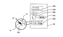
この際使用した計測装置は図1中に示されている、インピーダンスマッチング回路20a、サーキュレーター20b、高周波電源を含む発信器20c、アンプ20d、そしてディジタルオシロスコープ20e等を備えている。尚、発信器20cに代わり高周波受信アンテナを使用することもできる。
[第2の実施の形態]
図3には第2の実施の形態の弾性波素子10の外観が示されている。この弾性波素子10は弾性表面波が伝搬可能な曲面が連続した少なくとも円環状の曲面の一部によってなる伝搬帯12aを含む表面を有する3次元基体12と弾性波伝搬帯12c、および弾性波が反射可能であり、前記弾性表面波を励起し伝搬表面帯12aに沿い弾性表面波を励起するとともに伝搬表面帯12aに伝搬する前記弾性表面波を受信可能なすだれ状電極14と前記段弾性波を励起し弾性波伝搬帯12cに弾性波を励起するとともに弾性波伝搬帯12cに伝搬する前記弾性波を受信可能なすだれ状電極15を持つ。
The measurement apparatus used at this time includes an
[Second Embodiment]
FIG. 3 shows the appearance of the
この実施の形態において3次元基体12は3方晶系のニオブ酸リチウム結晶により形成されている。図3に示すように表面弾性波励起用の前記すだれ状電極14をニオブ酸リチウム結晶のZ軸からXY平面方向に90°の場所に、また弾性波励起用の前記すだれ状電極15をニオブ酸リチウム球基体のZ軸に形成し、それぞれに半値幅2nsのインパルスを印加したところ、音速3400m/sの表面弾性波と音速7400m/sのバルク波が観察された。
[第3の実施の形態]
図4には第3の実施の形態の弾性波素子10の外観が示されている。この弾性波素子10は弾性表面波が伝搬可能な曲面が連続した少なくとも円環状の曲面の一部によってなる伝搬帯12aを含む表面を有する3次元基体12と弾性波伝搬帯12c、および弾性波が反射可能な基質を持ち、前記弾性表面波を励起し伝搬表面帯12aに沿い弾性表面波を励起するとともに伝搬表面帯12aに伝搬する前記弾性表面波を受信可能でかつ、前記弾性波を励起し弾性波伝搬帯12cに弾性波を励起するとともに弾性波伝搬帯12cに伝搬する前記弾性波を受信可能なすだれ状電極16を持つ。
In this embodiment, the three-dimensional substrate 12 is formed of trigonal lithium niobate crystals. As shown in FIG. 3, the
[Third Embodiment]
FIG. 4 shows the appearance of the
この実施の形態において3次元基体12は3方晶系のニオブ酸リチウム結晶により形成されている。図4に示すように表面弾性波励起用の前記すだれ状電極16をニオブ酸リチウム結晶のZ軸からXY平面方向に20°に形成し半値幅2nsのインパルスを印加したところ、中心周波数210MHzで音速7400m/sのバルク波と中心周波数6.9MHzで音速3400m/sの表面弾性波が同時観測された。
[第4の実施の形態]
図5には第4の実施の形態の弾性波素子10の外観が示されている。この弾性波素子10は弾性表面波が伝搬可能な曲面が連続した少なくとも円環状の曲面の一部によってなる伝搬帯12aを含む表面を有する3次元基体12と弾性波伝搬帯12c、および弾性波が平行な1対の平坦部を持つ反射可能な基質を持ち、前記弾性表面波を励起し伝搬表面帯12aに沿い弾性表面波を励起するとともに伝搬表面帯12aに伝搬する前記弾性表面波を受信可能なすだれ状電極14と前記段弾性波を励起し弾性波伝搬帯12cに弾性波を励起するとともに弾性波伝搬帯12cに伝搬する前記弾性波を受信可能なすだれ状電極15を持つ。
In this embodiment, the three-dimensional substrate 12 is formed of trigonal lithium niobate crystals. As shown in FIG. 4, when the
[Fourth Embodiment]
FIG. 5 shows the appearance of the
この実施の形態において3次元基体12は3方晶系のニオブ酸リチウム結晶により形成されている。図3に示すように表面弾性波励起用の前記すだれ状電極14をニオブ酸リチウム結晶のZ軸からXY平面方向に90°の場所に、また弾性波励起用の前記すだれ状電極15をニオブ酸リチウム球基体のZ軸に形成し、それぞれに半値幅2nsのインパルスを印加したところ、中心周波数210MHz及び前記とは異なる中心周波数100〜200MHzで音速7400m/sのバルク波と中心周波数6.9MHzで音速3400m/sの表面弾性波が同時観測された。
[第3の変形例]
この発明に従った弾性波素子の第3の変形例について説明する。
In this embodiment, the three-dimensional substrate 12 is formed of trigonal lithium niobate crystals. As shown in FIG. 3, the
[Third Modification]
A third modification of the acoustic wave device according to the present invention will be described.
この変形例では、3次元基体状の1種類のすだれ状電極にて、バルク波と表面弾性波両方を励起、伝搬、多重周回或いは多重反射、受信するもので、励起信号をバルク波で保存し、環境差異を計測する表面波信号と比較し測定の精度の向上を図るものである。この実施の形態において3次元基体12は3方晶系のニオブ酸リチウム結晶を用いた。図4に示す装置でバルク波と表面波を同時に励起し、表面波が50周回った場合において、弾性波とバルク波の波形比較を行った。これにより表面弾性波の環境による差をこれまで以上に正確に測定できるようになった。
[第2、第3の変形例1]
この発明に従った弾性波素子の第2、及び第3の変形例について説明する。
In this modification, one type of interdigital electrode on a three-dimensional substrate is used to excite, propagate, multiplex or multi-reflect, and receive both bulk waves and surface acoustic waves. The excitation signal is stored as bulk waves. Compared with surface wave signals for measuring environmental differences, the measurement accuracy is improved. In this embodiment, the three-dimensional substrate 12 is a trigonal lithium niobate crystal. The bulk wave and the surface wave were excited simultaneously with the apparatus shown in FIG. 4, and the waveform comparison between the elastic wave and the bulk wave was performed when the surface wave turned around 50 times. As a result, the difference in surface acoustic wave due to the environment can be measured more accurately than before.
[Second and third modified examples 1]
Second and third modifications of the acoustic wave device according to the present invention will be described.
この変形例では3次元基体に2種類の異なるすだれ状電極より一方は表面弾性波、もう一方はバルク波を励起、伝搬、多重周回或いは多重反射、受信するもので。前記表面弾性波より環境差異を前記バルク波より素子温度を計測し、前記バルク波で計測した素子温度にて前記表面弾性波の音速をより正確なものとし環境の変化をより正確に高精度に検出した。この実施の形態において3次元基体12は3方晶系のニオブ酸リチウム結晶を用いた。図3に示すよにニオブ酸リチウムのZ軸にバルク波用すだれ状電極を、またZ軸からXY平面に90°のところに表面弾性波用すだれ状電極を形成した。今回はあらかじめ温度変化の可能な環境下でニオブ酸リチウムZ軸に設置したすだれ状電極にて体積熱膨張を考慮したバルク波の音速の温度変化を測定した、測定された温度変化は46ppm/℃であった。この実験より、素子の温度を0.1℃以内で補正がかけれることになり、表面弾性波の精度を5ppm以内にすることが出来た。
[第2、第3の実施例2]
第5の実施の形態は複数の弾性波素子に関するものである。図3より、この複数の弾性波素子10は弾性表面波が伝搬可能な曲面が連続した少なくとも円環状の曲面の一部によってなる伝搬帯12aを含む表面を有する3次元基体12と弾性波伝搬帯12c、および弾性波が反射可能な基質を持ち、前記弾性表面波を励起し複数伝搬表面帯12aに沿い弾性表面波を励起するとともに伝搬表面帯12aに伝搬する前記弾性表面波を受信可能なすだれ状電極14と前記段弾性波を励起し弾性波伝搬帯12cに弾性波を励起するとともに弾性波伝搬帯12cに伝搬する前記弾性波を受信可能なすだれ状電極15を持つ。このバルク波のすだれ状電極の電極幅をかえることにより、複数の素子に固有なバルク波の周波数を付加することが出来る。この実施の形態において3次元基体12は3方晶系のニオブ酸リチウム結晶により形成されている。弾性波励起用の前記すだれ状電極15をニオブ酸リチウム球基体のZ軸に形成し、電極幅を0.53mmのもと0.64mmのものとを準備した。2nsのインパルスを印可したことろ210MHzと170MHzのバルク波を確認した。双方の弾性波素子に同一の反応膜をつけ、環境差異検出装置をして動作させ平均を取ることにより、素子の性能の向上を計った。また、それぞれに素子に個別の反応膜をつけて、多チャンネル環境差異を検出する差異の素子識別にも持ちることができる。
In this modification, two types of interdigital electrodes on a three-dimensional substrate are used for exciting, propagating, multiplying or reflecting multiple times, and receiving the bulk acoustic wave. The environmental difference is measured from the surface acoustic wave, the element temperature is measured from the bulk wave, the sound velocity of the surface acoustic wave is made more accurate at the element temperature measured by the bulk wave, and the environmental change is made more accurately and accurately. Detected. In this embodiment, the three-dimensional substrate 12 is a trigonal lithium niobate crystal. As shown in FIG. 3, an interdigital electrode for bulk waves was formed on the Z axis of lithium niobate, and an interdigital electrode for surface acoustic waves was formed at 90 ° from the Z axis to the XY plane. This time, the temperature change of the sound velocity of the bulk wave was measured with the interdigital electrode installed on the lithium niobate Z-axis in an environment where the temperature change was possible in advance. The measured temperature change was 46ppm / ° C. Met. From this experiment, the temperature of the element can be corrected within 0.1 ° C., and the accuracy of the surface acoustic wave can be set within 5 ppm.
[Second and third embodiments 2]
The fifth embodiment relates to a plurality of acoustic wave elements. As shown in FIG. 3, the plurality of
10・・・弾性波素子
12・・・3次元基体
12a・・・伝搬表面帯
12c・・・内部伝搬帯
15・・・すだれ状電極
DESCRIPTION OF
Claims (9)
前記3次元基体の結晶軸のZ軸方向の基体表面に設置されたバルク波励起すだれ状電極と、を備え、 A bulk-wave-excited interdigital electrode placed on the surface of the substrate in the Z-axis direction of the crystal axis of the three-dimensional substrate,
前記バルク波励起すだれ状電極は、前記バルク波励起すだれ状電極が設置されたバルク波励起すだれ状電極設置基体表面と、前記バルク波励起すだれ状電極設置基体表面と対向する基体表面と、の間の基体内部をバルク波が多重反射する内部伝搬帯上に設置されていること The bulk-wave-excited interdigital electrode is formed between a bulk-wave-excited interdigital electrode-installed substrate surface on which the bulk-wave-excited interdigital electrode is disposed and a substrate surface opposite to the bulk-wave-excited interdigital electrode-installed substrate surface. It is installed on the internal propagation band where multiple reflections of bulk waves occur inside the substrate.
を特徴とする弾性波素子。An elastic wave device characterized by the above.
更に、 Furthermore,
前記伝搬表面帯上の3次元基体表面に、弾性表面波励起すだれ状電極と、を備えたこと A surface acoustic wave-excited interdigital electrode was provided on the surface of the three-dimensional substrate on the propagation surface zone.
を特徴とする請求項1に記載の弾性波素子。The acoustic wave device according to claim 1.
前記バルク波励起すだれ状電極は、前記伝搬表面帯と前記内部伝搬帯の交点となる3次元基体表面に設置されたこと The bulk-wave-excited interdigital electrode is installed on the surface of the three-dimensional substrate that is the intersection of the propagation surface band and the internal propagation band.
を特徴とする請求項1に記載の弾性波素子。The acoustic wave device according to claim 1.
前記バルク波励起すだれ状電極が設置されたバルク波励起すだれ状電極設置基体表面は、前記平坦面にあることThe bulk wave-excited interdigital electrode-installed substrate surface on which the bulk-wave-excited interdigital electrode is installed is on the flat surface.
を特徴とする請求項1または2のいずれかに記載の弾性波素子。The elastic wave device according to claim 1, wherein:
を特徴とする請求項1に記載の弾性波素子。The acoustic wave device according to claim 1.
前記内部伝搬帯は、Z軸方向からXY平面に対し75°までの範囲にあること The internal propagation band is in a range from the Z-axis direction to 75 ° with respect to the XY plane.
を特徴とする請求項3に記載の弾性波素子。The elastic wave device according to claim 3.
前記バルク波励起すだれ状電極および前記弾性表面波励起すだれ状電極に同一の入力信号を入力し、The same input signal is input to the bulk wave-excited interdigital electrode and the surface acoustic wave-excited interdigital electrode,
前記バルク波励起すだれ状電極からの出力信号と、前記弾性表面波励起すだれ状電極からの出力信号と、を比較することComparing the output signal from the bulk wave-excited interdigital electrode with the output signal from the surface acoustic wave-excited interdigital electrode
を特徴とする環境差異検出装置。Environmental difference detection device characterized by
前記バルク波励起すだれ状電極により温度を検出し、The temperature is detected by the bulk wave-excited interdigital electrode,
前記弾性表面波励起すだれ状電極により環境差異を検出することDetecting environmental differences with the surface acoustic wave-excited interdigital electrode
を特徴とする環境差異検出装置。Environmental difference detection device characterized by
複数の前記弾性波素子を用いたこと Using a plurality of the acoustic wave elements
を特徴とする環境差異検出装置。Environmental difference detection device characterized by
Priority Applications (1)
| Application Number | Priority Date | Filing Date | Title |
|---|---|---|---|
| JP2003380771A JP4389552B2 (en) | 2003-11-11 | 2003-11-11 | Acoustic wave element and environmental difference detection device using acoustic wave element |
Applications Claiming Priority (1)
| Application Number | Priority Date | Filing Date | Title |
|---|---|---|---|
| JP2003380771A JP4389552B2 (en) | 2003-11-11 | 2003-11-11 | Acoustic wave element and environmental difference detection device using acoustic wave element |
Publications (2)
| Publication Number | Publication Date |
|---|---|
| JP2005150784A JP2005150784A (en) | 2005-06-09 |
| JP4389552B2 true JP4389552B2 (en) | 2009-12-24 |
Family
ID=34690344
Family Applications (1)
| Application Number | Title | Priority Date | Filing Date |
|---|---|---|---|
| JP2003380771A Expired - Fee Related JP4389552B2 (en) | 2003-11-11 | 2003-11-11 | Acoustic wave element and environmental difference detection device using acoustic wave element |
Country Status (1)
| Country | Link |
|---|---|
| JP (1) | JP4389552B2 (en) |
Families Citing this family (1)
| Publication number | Priority date | Publication date | Assignee | Title |
|---|---|---|---|---|
| JP4789424B2 (en) * | 2004-03-31 | 2011-10-12 | 凸版印刷株式会社 | Gas pressure measuring device and gas pressure measuring method |
-
2003
- 2003-11-11 JP JP2003380771A patent/JP4389552B2/en not_active Expired - Fee Related
Also Published As
| Publication number | Publication date |
|---|---|
| JP2005150784A (en) | 2005-06-09 |
Similar Documents
| Publication | Publication Date | Title |
|---|---|---|
| US6293136B1 (en) | Multiple mode operated surface acoustic wave sensor for temperature compensation | |
| TWI251077B (en) | Saw sensor with improved temperature stability | |
| US7287431B2 (en) | Wireless oil filter sensor | |
| US20150013461A1 (en) | Device and method for measuring physical parameters using saw sensors | |
| US7788979B2 (en) | Monolithic antenna excited acoustic transduction device | |
| US7267009B2 (en) | Multiple-mode acoustic wave sensor | |
| JP7381167B2 (en) | differential sonic sensor | |
| RU2387051C1 (en) | Detector of physical value on surface acoustic waves | |
| JP2007524853A (en) | Layered surface acoustic wave sensor | |
| WO2005095947A1 (en) | Environment difference detector | |
| GB2426336A (en) | SAW based torque and temperature sensor | |
| AU2026200844A1 (en) | Multiplexing Surface Acoustic Wave Sensors with Delay Line Coding | |
| EP1453199B1 (en) | Surface acoustic wave element, electric signal processing apparatus using the surface acoustic wave element, and environment evaluation apparatus using the electric signal processing apparatus | |
| JP2008241542A (en) | Spherical surface acoustic wave sensor | |
| JP2020046257A (en) | Wireless temperature measurement system | |
| JP4337488B2 (en) | Method and apparatus for measuring drive of spherical surface acoustic wave device | |
| RU2585487C1 (en) | Passive temperature sensor operating on surface acoustic waves | |
| JP4389552B2 (en) | Acoustic wave element and environmental difference detection device using acoustic wave element | |
| JP4727968B2 (en) | Surface acoustic wave element identification device and acoustic wave element identification device | |
| JP2007225546A (en) | Surface acoustic wave sensor | |
| JP2005191650A (en) | Surface acoustic wave device using langasite crystal and environmental difference detection device using surface acoustic wave device | |
| JP2008180668A (en) | Lamb wave type high frequency sensor device | |
| JP2017062699A (en) | Sensing system | |
| JP7351508B2 (en) | Recognition signal generation element and element recognition system | |
| KR102314169B1 (en) | Apparatus for chemosensing and Method for measuring apparatus |
Legal Events
| Date | Code | Title | Description |
|---|---|---|---|
| A621 | Written request for application examination |
Free format text: JAPANESE INTERMEDIATE CODE: A621 Effective date: 20061024 |
|
| A977 | Report on retrieval |
Free format text: JAPANESE INTERMEDIATE CODE: A971007 Effective date: 20090319 |
|
| A131 | Notification of reasons for refusal |
Free format text: JAPANESE INTERMEDIATE CODE: A131 Effective date: 20090407 |
|
| A521 | Written amendment |
Free format text: JAPANESE INTERMEDIATE CODE: A523 Effective date: 20090522 |
|
| TRDD | Decision of grant or rejection written | ||
| A01 | Written decision to grant a patent or to grant a registration (utility model) |
Free format text: JAPANESE INTERMEDIATE CODE: A01 Effective date: 20090915 |
|
| A01 | Written decision to grant a patent or to grant a registration (utility model) |
Free format text: JAPANESE INTERMEDIATE CODE: A01 |
|
| A61 | First payment of annual fees (during grant procedure) |
Free format text: JAPANESE INTERMEDIATE CODE: A61 Effective date: 20090928 |
|
| FPAY | Renewal fee payment (event date is renewal date of database) |
Free format text: PAYMENT UNTIL: 20121016 Year of fee payment: 3 |
|
| R150 | Certificate of patent or registration of utility model |
Free format text: JAPANESE INTERMEDIATE CODE: R150 |
|
| FPAY | Renewal fee payment (event date is renewal date of database) |
Free format text: PAYMENT UNTIL: 20131016 Year of fee payment: 4 |
|
| LAPS | Cancellation because of no payment of annual fees |