JP4386262B2 - Image forming apparatus - Google Patents
Image forming apparatus Download PDFInfo
- Publication number
- JP4386262B2 JP4386262B2 JP2004028529A JP2004028529A JP4386262B2 JP 4386262 B2 JP4386262 B2 JP 4386262B2 JP 2004028529 A JP2004028529 A JP 2004028529A JP 2004028529 A JP2004028529 A JP 2004028529A JP 4386262 B2 JP4386262 B2 JP 4386262B2
- Authority
- JP
- Japan
- Prior art keywords
- power
- temperature
- fixing
- power supply
- supplied
- Prior art date
- Legal status (The legal status is an assumption and is not a legal conclusion. Google has not performed a legal analysis and makes no representation as to the accuracy of the status listed.)
- Expired - Fee Related
Links
Images


Classifications
-
- G—PHYSICS
- G03—PHOTOGRAPHY; CINEMATOGRAPHY; ANALOGOUS TECHNIQUES USING WAVES OTHER THAN OPTICAL WAVES; ELECTROGRAPHY; HOLOGRAPHY
- G03G—ELECTROGRAPHY; ELECTROPHOTOGRAPHY; MAGNETOGRAPHY
- G03G15/00—Apparatus for electrographic processes using a charge pattern
- G03G15/20—Apparatus for electrographic processes using a charge pattern for fixing, e.g. by using heat
- G03G15/2003—Apparatus for electrographic processes using a charge pattern for fixing, e.g. by using heat using heat
- G03G15/2014—Apparatus for electrographic processes using a charge pattern for fixing, e.g. by using heat using heat using contact heat
- G03G15/2039—Apparatus for electrographic processes using a charge pattern for fixing, e.g. by using heat using heat using contact heat with means for controlling the fixing temperature
-
- G—PHYSICS
- G03—PHOTOGRAPHY; CINEMATOGRAPHY; ANALOGOUS TECHNIQUES USING WAVES OTHER THAN OPTICAL WAVES; ELECTROGRAPHY; HOLOGRAPHY
- G03G—ELECTROGRAPHY; ELECTROPHOTOGRAPHY; MAGNETOGRAPHY
- G03G15/00—Apparatus for electrographic processes using a charge pattern
- G03G15/80—Details relating to power supplies, circuits boards, electrical connections
-
- G—PHYSICS
- G03—PHOTOGRAPHY; CINEMATOGRAPHY; ANALOGOUS TECHNIQUES USING WAVES OTHER THAN OPTICAL WAVES; ELECTROGRAPHY; HOLOGRAPHY
- G03G—ELECTROGRAPHY; ELECTROPHOTOGRAPHY; MAGNETOGRAPHY
- G03G2215/00—Apparatus for electrophotographic processes
- G03G2215/00978—Details relating to power supplies
- G03G2215/00983—Details relating to power supplies using batteries
-
- G—PHYSICS
- G03—PHOTOGRAPHY; CINEMATOGRAPHY; ANALOGOUS TECHNIQUES USING WAVES OTHER THAN OPTICAL WAVES; ELECTROGRAPHY; HOLOGRAPHY
- G03G—ELECTROGRAPHY; ELECTROPHOTOGRAPHY; MAGNETOGRAPHY
- G03G2215/00—Apparatus for electrophotographic processes
- G03G2215/20—Details of the fixing device or porcess
- G03G2215/2003—Structural features of the fixing device
- G03G2215/2016—Heating belt
- G03G2215/2035—Heating belt the fixing nip having a stationary belt support member opposing a pressure member
Abstract
Description
本発明は、電子写真プロセス等を利用した画像形成装置に関する。 The present invention relates to an image forming apparatus using an electrophotographic process or the like.
レーザビームプリンタ等の電子写真プロセスを用いた画像形成装置には、記録媒体(記録紙やOHPシートなど)に形成されたトナー像を熱溶融させて定着させる定着器が設けられている。この定着器における加熱方式としてはいくつかのタイプがある。とりわけ、磁束により定着ローラに電流を誘導させ、そのジュール熱によって発熱させる電磁誘導加熱方式は、誘導電流の発生を利用することで直接定着ローラを発熱させることができ、ハロゲンランプを熱源として用いた熱ローラ方式の定着装置よりも高効率の定着プロセスを達成できる点で有利である(例えば、特許文献1を参照。)。 2. Description of the Related Art Image forming apparatuses using an electrophotographic process such as a laser beam printer are provided with a fixing device that heats and fixes a toner image formed on a recording medium (recording paper, OHP sheet, etc.). There are several types of heating systems in this fixing device. In particular, the electromagnetic induction heating method in which current is induced in the fixing roller by magnetic flux and heat is generated by the Joule heat can directly heat the fixing roller by using the generation of induced current, and a halogen lamp is used as a heat source. This is advantageous in that it can achieve a more efficient fixing process than a heat roller type fixing device (see, for example, Patent Document 1).
ところで、例えばA4サイズの定型紙を16枚/分の速度で印字可能とするようなカラー画像形成装置(A4機)においては近年、上記したような電磁誘導加熱方式の熱容量の小さな定着器を使用することで、待機時の定着温度調節(以下、「温度調節」を「温調」と略記することもある。)が不要で、プリント時にのみ過熱を行ういわゆる「オンデマンド定着」を実現することが可能となっている。 By the way, in a color image forming apparatus (A4 machine) capable of printing A4 size standard paper at a speed of 16 sheets / minute, for example, a fixing device having a small heat capacity as described above has recently been used. By doing so, it is not necessary to adjust the fixing temperature during standby (hereinafter, “temperature adjustment” may be abbreviated as “temperature adjustment”), and so-called “on-demand fixing” in which overheating is performed only during printing. Is possible.
一方、A3サイズの定型紙まで印字可能とするようなカラー画像形成装置(A3機)においては、その印刷スピードに依存するものの、一般にA4機よりは定着器に求められる熱容量が大きいため、待機時においても所定の時間間隔で電力を定着器に供給することで予熱を行ういわゆる「スタンバイ温調」がなされている(例えば、特許文献2を参照)。スタンバイ温調を行う理由は次のとおりである。 On the other hand, in a color image forming apparatus (A3 machine) capable of printing up to A3 size standard paper, although it depends on the printing speed, since the heat capacity required for the fixing device is generally larger than that of the A4 machine, Also, the so-called “standby temperature control” is performed in which preheating is performed by supplying power to the fixing device at predetermined time intervals (see, for example, Patent Document 2). The reason for performing standby temperature control is as follows.
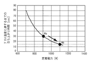
図27は、従来の電磁誘導加熱方式の定着器を用いたカラー画像形成装置(A3機)において、定着器の冷えた状態からプリント可能状態の温度(例えば180℃)に達するまでの立ち上がり時間とその時に定着器のヒータに供給した電力(定着電力)との関係を示している。同図において、供給可能な定着電力が約900Wであるとすると、プリント可能状態の温度(プリント温度)に達するまでの立ち上がり時間は30sec(点Wa)となっている。この時間は一般的に用いられるハロゲンヒータを用いた定着器に比べて極めて短時間である。しかしながら、紙の搬送時間等を考慮すると、プリント開始から一枚目の画像形成済みの紙が排紙部に排出されるまでの時間(ファーストプリントアウトタイム)は30secよりも遅くなりユーザを待たせてしまう。このため、ファーストプリントアウトタイムを短縮するために、(ハロゲンヒータ方式の定着器を用いた画像形成装置で一般的に行われているように、)待機時においても所定の時間間隔で電力を定着器に供給することで予熱を行う。このスタンバイ温調を実施することにより、プリントジョブを開始してから画像形成可能な所定の定着温度に早く到達させるようにしている。 FIG. 27 shows a rise time until the temperature reaches a printable state (for example, 180 ° C.) from a cool state of the fixing device in a color image forming apparatus (A3 machine) using a conventional electromagnetic induction heating type fixing device. The relationship with the electric power (fixing electric power) supplied to the heater of the fixing device at that time is shown. In the figure, assuming that the fixing power that can be supplied is about 900 W, the rise time until reaching the temperature of the printable state (printing temperature) is 30 sec (point Wa). This time is extremely short compared with a fixing device using a generally used halogen heater. However, considering the paper transport time, the time from the start of printing until the first image-formed paper is discharged to the paper discharge unit (first print out time) is later than 30 sec, and the user is kept waiting. End up. For this reason, in order to shorten the first printout time, the power is fixed at predetermined time intervals even during standby (as is generally done in an image forming apparatus using a halogen heater type fixing device). Preheating is performed by supplying to the vessel. By performing this standby temperature control, a predetermined fixing temperature at which an image can be formed is quickly reached after a print job is started.
電磁誘導加熱方式におけるこのようなスタンバイ温調時の消費電力は、ハロゲンヒータを用いた定着方式と比較するとスタンバイ温調時の温度を低く設定することができるため、小さな電力消費に抑えることが可能であるものの、オンデマンド定着方式と比較する場合には余分な電力(スタンバイ温調時の電力)が必要であることには変わりない。 The power consumption during standby temperature adjustment in the electromagnetic induction heating method can be set to a lower temperature compared to the fixing method using a halogen heater, so the power consumption during the standby temperature adjustment can be reduced. However, when compared with the on-demand fixing method, there is no change in that extra power (power during standby temperature control) is required.
ところで、この画像形成装置において、定着器のヒータへの供給電力を約200W増加させることが可能であれば、定着器に1100W投入することができプリント温度に達するまでの時間は約15sec(図中の点Wb)となる。このため、この画像形成装置が目標とするファーストプリントアウトタイムが、仮に20sec程度であれば、(画像形成装置の構成、紙搬送経路や搬送速度等に依存するものの、)スタンバイ温調が不要なオンデマンド定着を実現することも可能である。 By the way, in this image forming apparatus, if the power supplied to the heater of the fixing device can be increased by about 200 W, 1100 W can be supplied to the fixing device, and the time required to reach the printing temperature is about 15 seconds (in the drawing). Point Wb). For this reason, if the first printout time targeted by the image forming apparatus is about 20 seconds, standby temperature control is not necessary (although it depends on the configuration of the image forming apparatus, the paper conveyance path, the conveyance speed, etc.). It is also possible to achieve on-demand fixing.
しかしながら最近では、画像形成装置の技術向上に伴い、これまで中速機(中級機)のカテゴリの画像形成装置が小型化、低価格化されながらも高速化され、一昔前の高速機の速度に達してきている。それに伴って、省エネルギー化、ファーストプリントアウトタイム短縮等の付加価値がこれまで以上に市場から求められるようになってきている。 Recently, however, as the technology of image forming apparatuses has improved, image forming apparatuses in the category of medium speed machines (intermediate machines) have been speeded up while being downsized and reduced in price. Has reached. Along with this, added value such as energy saving and shortening the first printout time has been increasingly demanded from the market.
このような背景を考慮すると、高効率な電磁誘導加熱方式の定着器を用いたとしても、従来A4機において実現可能であったオンデマンド定着では市場の要求に応えることが難しくなってきている。 Considering such a background, even if a high-efficiency electromagnetic induction heating type fixing device is used, it has become difficult to meet market demands with on-demand fixing that could be realized with the conventional A4 machine.
また、A3機において従来行ってきたスタンバイ温調は、上記したように、必要最小限度の電力とはいえ待機時においても定着器に電力を投入していることになるため、このスタンバイ温調が、画像形成装置の待機時における消費電力の軽減が困難である要因の一つでもあった。 Further, as described above, the standby temperature control that has been conventionally performed in the A3 machine is that the power is supplied to the fixing device even in the standby state even though it is the minimum necessary power. This is one of the factors that make it difficult to reduce power consumption during standby of the image forming apparatus.
かといって、スタンバイ時の省エネルギー化を重視してこのスタンバイ温調制御を実施しないことにすると、プリント開始から画像形成可能な所定の定着温度に達するまでの時間が長くかかるため、結果として、ファーストプリントアウトタイムが遅くなってしまうという問題に直面することになる。つまり、待機時における省エネルギー化とファーストプリントアウトタイムの短縮とはトレードオフの関係にある。 However, if this standby temperature adjustment control is not performed with emphasis on energy saving during standby, it takes a long time to reach a predetermined fixing temperature at which image formation is possible from the start of printing. You will face the problem of slow printout time. That is, there is a trade-off between energy saving during standby and shortening of the first printout time.
したがって、待機時における省エネルギー化とファーストプリントアウトタイムの短縮の両者のバランスを取った上で、市場に受け入れられるレベルの、温度の立ち上がりの早いオンデマンド定着システムを開発する必要がある。 Therefore, it is necessary to develop an on-demand fixing system that can be accepted in the market and has a fast rise in temperature while balancing energy saving during standby and shortening the first printout time.
一方、モノクロ高速印刷機やカラー印刷高画質機等の大型でかつ高付加価値の画像形成装置、いわゆる高速機(高級機)は、省エネルギー化の工夫はなされているものの、高機能化やオプション装置の充実等の更なる付加価値が求められおり、消費電力は増加していく方向にある。これら機器の消費する電力の上限の一つの目安としては、商用電源で供給可能な最大電流がある。例えば、電圧100Vの商用電源について、15Aの最大供給電流が規定されている場合には、その電力の上限は1500W(=100V×15A)となる。画像形成装置本体においては、装置の最大電流が商用電源の最大電流を超えないように設計するのが通常である。 On the other hand, large-scale and high-value-added image forming devices such as monochrome high-speed printers and color printing high-quality printers, so-called high-speed machines (high-end machines), have been devised to save energy, but have high functionality and optional equipment. There is a demand for further added value such as enhancement of power consumption, and power consumption is increasing. One guideline for the upper limit of power consumed by these devices is the maximum current that can be supplied by commercial power. For example, if a maximum supply current of 15 A is specified for a commercial power supply with a voltage of 100 V, the upper limit of the power is 1500 W (= 100 V × 15 A). The image forming apparatus main body is usually designed so that the maximum current of the apparatus does not exceed the maximum current of the commercial power source.
また、この高速機クラスの定着器では、高速連続定着に耐え得るよう一般に熱容量の大きな定着器が用いられることが多い。このような定着器のデメリットは、定着器が冷えた状態からスタンバイ状態の温度に達するまでの時間(ウォームアップ時間)に長時間(数分)を要する点であり、このウォームアップ時間の短縮が改善課題の一つであった。 Further, in this high speed machine class fixing device, a fixing device having a large heat capacity is generally used so as to withstand high speed continuous fixing. The disadvantage of such a fuser is that it takes a long time (several minutes) to reach the standby temperature (warm-up time) from the cold state of the fuser, and this shortens the warm-up time. It was one of the improvement issues.
これに対し、単純に大電力を投入して定着器のウォームアップ時間を短縮しようとすると、商用電源の最大電力が装置として使用可能な電力の上限が制約となるため、定着システム自体の改善を行わない限り、さらにウォームアップ時間を短縮することは困難であった。 On the other hand, if you try to reduce the warm-up time of the fuser simply by turning on a large amount of power, the maximum power of the commercial power supply will be limited by the upper limit of the power that can be used as a device. Unless done, it was difficult to further reduce the warm-up time.
このような問題を解決する一つの手段として、例えば実公平7−41023号公報(特許文献3)では、定着器への電力を有効活用するために、定着器に主ヒータと副ヒータを備えた画像形成装置に蓄電部を設け、蓄電部は直流電源あるいは直流モータ制御部に選択的に接続することを提案している。すなわち、蓄電部から直流モータに電力が供給されている間は、直流モータに供給されるはずの電力を副ヒータに供給できるため定着器の温度を従来よりも上げることができ、この間は高速で複写できるようになっている。 As one means for solving such a problem, for example, Japanese Utility Model Publication No. 7-41023 (Patent Document 3) includes a main heater and a sub-heater in a fixing device in order to effectively use power to the fixing device. It has been proposed that a power storage unit is provided in the image forming apparatus, and the power storage unit is selectively connected to a DC power source or a DC motor control unit. That is, while power is being supplied from the power storage unit to the DC motor, the power to be supplied to the DC motor can be supplied to the sub-heater, so that the temperature of the fixing device can be raised compared to the conventional case. It can be copied.
また、特開2002−174988号公報(特許文献4)では、画像形成装置に蓄電装置を設け、定着器の立上げ時に商用電源からの電力と蓄電装置からの電力を併用することにより、省エネルギーとプリント開始時間の短縮を図る方法が提案されている。 In Japanese Patent Laid-Open No. 2002-174988 (Patent Document 4), an energy storage device is provided in an image forming apparatus, and energy saving is achieved by using both power from a commercial power source and power from the power storage device when the fixing device is started up. A method for shortening the print start time has been proposed.
このように、従来から、蓄電装置を用いた画像形成装置が知られているが、その蓄電装置に関連し、更なる有効活用が望まれていた。As described above, an image forming apparatus using a power storage device is conventionally known. However, further effective utilization has been desired in connection with the power storage device.
上記した課題は、本発明の画像形成装置によって解決される。本発明の一側面は例えば、商用電源から供給される電力を利用して発熱する発熱体を内包し、トナー画像が形成された転写材にその発熱体の熱を加えることで前記トナー画像を前記転写材に定着させる定着手段を備えた画像形成装置に係り、前記発熱体以外の負荷に電力を供給可能な蓄電手段と、前記定着手段の温度を検出する温度検出手段と、前記温度検出手段による検出結果に応じて、商用電源から前記定着手段への供給電力を制御する制御手段とを有し、前記制御手段は、電源投入時または省エネルギーモードからの復帰時に前記温度検出手段による温度検出を実行し、検出した前記定着手段の温度が所定温度未満である場合は、前記蓄電手段からの電力を前記駆動負荷に供給することで、商用電源から前記定着手段への供給電力を増加させ、前記蓄電手段からの電力が前記駆動負荷に供給されている間、前記温度検出手段による温度検出を繰り返すことで前記定着手段の温度を監視し、前記定着手段の温度が前記所定温度以上となった場合は、前記蓄電手段から前記駆動負荷への電力供給を遮断することで、商用電源から前記定着手段への供給電力を減少させることを特徴とする。
本発明の別の側面によれば、商用電源から供給される電力を利用して発熱する発熱体を内包し、トナー画像が形成された転写材にその発熱体の熱を加えることで前記トナー画像を前記転写材に定着させる定着手段を備えた画像形成装置であって、前記発熱体以外の負荷に電力を供給可能な蓄電手段と、前記定着手段の温度を検出する温度検出手段と、前記蓄電手段の蓄電量を検出する蓄電量検出手段と、前記温度検出手段による検出結果および前記蓄電量検出手段による検出結果に応じて、商用電源から前記定着手段への供給電力を制御する制御手段とを有し、前記制御手段は、電源投入時または省エネルギーモードからの復帰時に前記温度検出手段による温度検出及び前記蓄電量検出手段による蓄電量検出を実行し、検出した前記定着器の温度が所定温度未満であり、かつ、検出した前記蓄電手段の蓄電量が所定量以上ある場合は、前記蓄電手段からの電力を前記駆動負荷に供給することで、商用電源から前記定着手段への供給電力を増加させ、前記蓄電手段からの電力を前記駆動負荷に供給している間、前記蓄電量検出手段による蓄電量検出及び前記温度検出手段による温度検出を繰り返すことで前記蓄電手段の蓄電量及び前記定着手段の温度を監視し、前記蓄電手段の蓄電量が前記所定量未満となり、または、前記定着器の温度が前記所定温度以上となった場合は、前記蓄電手段から前記駆動負荷への電力供給を遮断することで、商用電源から前記定着手段への供給電力を減少させることを特徴とする画像形成装置が提供される。
The above problems are solved by the image forming apparatus of the present invention. One aspect of the present invention includes, for example, a heating element that generates heat using electric power supplied from a commercial power source, and applies the heat of the heating element to a transfer material on which a toner image is formed, thereby converting the toner image into the toner image. According to an image forming apparatus including a fixing unit for fixing to a transfer material, a power storage unit capable of supplying electric power to a load other than the heating element, a temperature detecting unit for detecting a temperature of the fixing unit, and the temperature detecting unit depending on the detection result, it has a control means for controlling the power supplied to the fixing unit from the commercial power source, the control means executes the temperature detection by the temperature detecting means when returning from power-on or the energy saving mode When the detected temperature of the fixing unit is lower than a predetermined temperature, the power supplied from the power storage unit is supplied to the driving load, thereby increasing the power supplied from a commercial power source to the fixing unit. The temperature of the fixing unit is monitored by repeating temperature detection by the temperature detecting unit while the electric power from the power storage unit is supplied to the driving load, and the temperature of the fixing unit is equal to or higher than the predetermined temperature. In this case, the power supplied from the power storage unit to the driving load is cut off, thereby reducing the power supplied from a commercial power source to the fixing unit .
According to another aspect of the present invention, the toner image includes a heating element that generates heat using electric power supplied from a commercial power source, and heat is applied to the transfer material on which the toner image is formed. An image forming apparatus including a fixing unit that fixes the toner onto the transfer material, a power storage unit capable of supplying power to a load other than the heating element, a temperature detection unit that detects a temperature of the fixing unit, and the power storage Storage amount detection means for detecting the storage amount of the means, and control means for controlling the power supplied from the commercial power source to the fixing means according to the detection result by the temperature detection means and the detection result by the storage amount detection means. And the control means executes temperature detection by the temperature detection means and power storage amount detection by the power storage amount detection means when power is turned on or when returning from the energy saving mode, and the detected fixing device When the temperature is less than a predetermined temperature and the detected storage amount of the power storage unit is equal to or greater than a predetermined amount, power from the power storage unit is supplied to the driving load, so that a commercial power source can supply the fixing unit. While increasing the supplied power and supplying the power from the power storage means to the driving load, the power storage amount of the power storage means is repeated by repeatedly detecting the power storage amount by the power storage amount detection means and the temperature detection by the temperature detection means. And the temperature of the fixing unit is monitored, and when the amount of power stored in the power storage unit is less than the predetermined amount, or the temperature of the fixing unit is equal to or higher than the predetermined temperature, the power storage unit supplies the driving load. An image forming apparatus is provided that reduces power supplied from a commercial power source to the fixing unit by cutting off power supply.
本発明の別の側面は例えば、商用電源から供給される電力を利用して発熱する発熱体を内包し、トナー画像が形成された転写材にその発熱体の熱を加えることで前記トナー画像を前記転写材に定着させる定着器を有する画像形成装置に係り、商用電源の交流電圧を所定の直流電圧に降圧して出力する電源回路と、充放電可能な蓄電器と、前記蓄電器からの出力電圧を所定の昇圧レベルに昇圧して出力する定電圧制御回路と、商用電源及び前記蓄電器から前記発熱体以外の負荷への電力供給を制御する制御回路と、商用電源からの電力を前記制御回路による制御状態に応じた制限レベルに制限して、前記定着器に供給する定着制御回路と、前記定着器の温度を検出する温度検出素子と、電源投入時又は省エネルギーモードからの復帰時に前記温度検出素子により検出された前記定着器の温度が所定温度未満である場合、前記制御回路により前記蓄電器からの電力を前記定電圧制御回路を介して前記負荷に供給させ、これに応じて前記定着制御回路に前記制限レベルを上昇させる第1の調整回路と、前記蓄電器からの電力が前記定電圧制御回路を介して前記駆動負荷に供給されている間、前記温度検出素子により検出される前記定着器の温度を監視し、前記定着器の温度が前記所定温度以上となった場合、前記制御回路により商用電源からの電力を前記電源回路を介して前記負荷に供給させ、これに応じて前記定着制御回路に前記制限レベルを降下させる第2の調整回路とを有することを特徴とする。
本発明の更に別の側面は、商用電源から供給される電力を利用して発熱する発熱体を内包し、トナー画像が形成された転写材にその発熱体の熱を加えることで前記トナー画像を前記転写材に定着させる定着手段を有する画像形成装置に係り、充放電可能な蓄電手段と、前記定着手段の温度の値を検出する温度検出手段と、前記定着手段以外の負荷を作動させるための電力供給を前記蓄電手段に行わせている場合には、前記定着手段以外の負荷を作動させるための電力供給を前記蓄電手段に行わせず前記商用電源に行わせている場合と比べ、前記商用電源から前記定着手段への電力供給を増加させるよう制御する制御手段とを有し、前記制御手段は、前記温度検出手段による検出結果の値が所定値以上のときには、前記定着手段以外の負荷を作動させるための電力供給を前記蓄電手段に行わせず前記商用電源に行わせる一方、前記温度検出手段による検出結果の値が前記所定値未満のときには、前記定着手段以外の負荷を作動させるための電力供給を前記蓄電手段に行わせることを特徴とする。
Another aspect of the present invention includes, for example, a heating element that generates heat using electric power supplied from a commercial power source, and applies the heat of the heating element to a transfer material on which a toner image is formed, thereby converting the toner image. The present invention relates to an image forming apparatus having a fixing device that fixes a transfer material, a power supply circuit that steps down and outputs an AC voltage of a commercial power supply to a predetermined DC voltage, a chargeable / dischargeable capacitor, and an output voltage from the capacitor. A constant voltage control circuit that boosts and outputs to a predetermined boost level, a control circuit that controls power supply from a commercial power source and the capacitor to a load other than the heating element, and control of power from the commercial power source by the control circuit A fixing control circuit that supplies the fixing device with a restriction level according to a state, a temperature detecting element that detects the temperature of the fixing device, and the temperature when the power is turned on or when returning from the energy saving mode. When the temperature of the fixing device detected by the detection element is lower than a predetermined temperature, the control circuit causes the electric power from the storage device to be supplied to the load via the constant voltage control circuit, and the fixing control is performed accordingly. A first adjustment circuit that raises the limit level to the circuit; and the fixing device that is detected by the temperature detection element while power from the battery is being supplied to the driving load via the constant voltage control circuit. When the temperature of the fixing device becomes equal to or higher than the predetermined temperature, the control circuit supplies power from a commercial power source to the load via the power circuit, and the fixing control is accordingly performed. And a second adjustment circuit for lowering the limit level in the circuit.
Still another aspect of the present invention includes a heating element that generates heat using electric power supplied from a commercial power source, and applies the heat of the heating element to a transfer material on which a toner image is formed, thereby forming the toner image. The present invention relates to an image forming apparatus having a fixing unit for fixing to a transfer material, a chargeable / dischargeable power storage unit, a temperature detecting unit for detecting a temperature value of the fixing unit, and a load for operating a load other than the fixing unit. In the case where power is supplied to the power storage unit, the commercial power supply is compared with the case where the power supply for operating a load other than the fixing unit is not supplied to the power storage unit. have a control means for controlling so as to increase the supply of electric power from the power supply to the fixing unit, wherein, when the value of the detection result of the temperature detecting means is above a predetermined value, the loads other than the fixing unit Product Power for causing the power storage means not to supply the commercial power source, but when the value of the detection result by the temperature detection means is less than the predetermined value, the power for operating a load other than the fixing means Supply is performed by the power storage means .
本発明によれば、商用電源の上限電流(電力)をより有効活用して、これまで以上に温度の立ち上がりの早いオンデマンド定着を実現可能な画像形成装置を提供することができる。 According to the present invention, it is possible to provide an image forming apparatus capable of more effectively utilizing the upper limit current (electric power) of a commercial power supply and realizing on-demand fixing with a temperature rise faster than ever.
以下、図面を参照して本発明の好適な実施形態について詳細に説明する。なお、以下では本発明の一実施形態としてレーザビームプリンタを例にとって説明する。ただし、本発明はレーザビームプリンタに限定されるものではなく、電子写真プロセスを使用した画像形成装置全般に適用することができる。 DESCRIPTION OF EMBODIMENTS Hereinafter, preferred embodiments of the present invention will be described in detail with reference to the drawings. In the following, a laser beam printer will be described as an example of an embodiment of the present invention. However, the present invention is not limited to the laser beam printer, and can be applied to all image forming apparatuses using an electrophotographic process.
■ 第1の実施形態 ■ ■ First Embodiment ■
<レーザビームプリンタ100の概略構成>
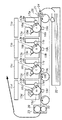
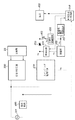
図1は、本発明の実施形態に係るレーザビームプリンタ100の概略構成を示す図である。このレーザビームプリンタ100は、黒画像(Bk),イエロー画像(Y),マゼンタ画像(M),シアン(C)画像の各色ごとに画像形成部を設けているいわゆるタンデムタイプのプリンタである。
<Schematic Configuration of
FIG. 1 is a diagram showing a schematic configuration of a
それぞれの画像形成部は、感光体ドラム18、感光ドラムを一様に帯電する一次帯電器16、感光体ドラム上に潜像を形成するスキャナユニット11、潜像を現像して可視像とする現像器14、可視像を転写紙に転写する転写器19、感光体の残留トナーを除去するクリーニング装置15等で構成される。 Each image forming unit includes a photosensitive drum 18, a primary charger 16 for uniformly charging the photosensitive drum, a scanner unit 11 for forming a latent image on the photosensitive drum, and developing the latent image into a visible image. The developing unit 14, a transfer unit 19 that transfers a visible image onto transfer paper, a cleaning device 15 that removes residual toner on the photosensitive member, and the like.
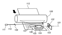
ここでスキャナユニット11の構成について説明しておく。図2は、スキャナユニット11の構成を示す図である。パーソナルコンピュータ等の図示しない外部機器からの画像形成指示があると、レーザビームプリンタ100内のコントローラ(図示せず)において、画像情報が露光手段であるレーザビームをオン/オフするための画像信号(VDO信号)101に変換される。この画像信号(VDO信号)101は、スキャナユニット11内のレーザユニット102に入力される。103は、レーザユニット102によりオン/オフ変調されたレーザビームである。104は、回転多面鏡(ポリゴンミラー)105を定常回転させるスキャナモータである。106は、ポリゴンミラーによって変更されたレーザビーム107を被走査面である感光ドラム18上に焦点を結ばせる結像レンズである。
Here, the configuration of the scanner unit 11 will be described. FIG. 2 is a diagram illustrating a configuration of the scanner unit 11. When there is an image formation instruction from an external device (not shown) such as a personal computer, a controller (not shown) in the
この構成により、画像信号101により変調されたレーザビーム13が感光ドラム18上を水平走査(主走査方向への走査)し、感光ドラム18上に潜像が形成される。
With this configuration, the laser beam 13 modulated by the
109はビーム検出口で、スリット状の入射口よりビームを取り入れる。この入射口より入ったレーザビームは、光ファイバ110内を通って光電変換素子111に導かれる。光電変換素子111により電気信号に変換されたレーザビームは、増幅回路(図示しない)により増幅された後、水平同期信号となる。
説明を図1に戻す。カセット22から給紙される記録媒体としての転写紙は、画像形成部とタイミングをとるために、レジストローラ21で待機する。
Returning to FIG. The transfer sheet as a recording medium fed from the
また、レジストローラ21の近傍には、給紙された転写紙の先端を検知するためのレジセンサ24が設けてある。画像形成部を制御する画像形成制御部(図示せず)はレジセンサ24の検出結果により、紙の先端がレジストローラ21に到達したタイミングを検知し、1色目(図の例ではイエロー色)の像を、像担持体である感光ドラム18a上に形成するとともに、定着器23のヒータ(図示しない)温度が所定の温度になるよう制御する。
A
29は吸着ローラであり、このローラの軸に吸着バイアスを印可し、転写紙を搬送ベルト20上に静電的に吸着させる。
レジストローラ21で待機した転写紙は、レジセンサ24の検出結果と像形成プロセスとのタイミングをとって、各色画像形成部を貫通するように配置された転写ベルト20上を搬送されるとともに、転写器19aにより1色目の画像が転写紙上に転写される。
The transfer paper waiting on the
同様に、2色目(図の例ではマゼンタ)の像は、レジセンサ24の検出結果と、2色目像形成プロセスとのタイミングをとって、転写ベルト20上を搬送される転写紙上の、1色目の像の上に重畳転写される。以降同様に、3色目(図の例ではシアン)の像,4色目(図の例では黒色)の像が、各像形成プロセスとのタイミングを取って、転写紙上に順次重畳転写される。
Similarly, the image of the second color (magenta in the example in the figure) is obtained by taking the timing of the detection result of the
そして、トナー画像が転写された転写紙は定着器23へと搬送され、その転写紙が定着器23におけるニップ部N(詳細は後述する)を通過することにより、トナーが加圧、過熱されて転写紙に溶融定着される。定着器23を通過した転写紙は機外に排紙されフルカラーの画像形成が終了する。
Then, the transfer paper on which the toner image is transferred is conveyed to the fixing
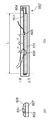
<定着器23の構成>
本実施形態における定着器23では、ハロゲンランプを熱源として用いた熱ローラ方式よりも高効率な、電磁誘導加熱方式を採用する。ここでは図4〜6を参照して定着器23の構造例を説明する。図4は定着器23の要部の横断面構造を示す構成図、図5は定着器23の要部の正面構造を示す構成図、図6は定着器23を構成する定着ベルトガイド部材を示す斜視図である。
<Configuration of
The fixing
501は電磁誘導発熱層(導電体層、磁性体層、抵抗体層)を有する電磁誘導発熱性の回転体としての円筒状の定着ベルトである。この定着ベルト501の具体的な構造例については後述する。
516aは横断面略半円弧状樋型のベルトガイド部材であり、円筒状の定着ベルト501はこのベルトガイド部材516aの外側にルーズに外嵌させてある。ベルトガイド部材516aは基本的に、(1)後述する加圧ローラ530との圧接により形成される定着ニップ部Nへの加圧、(2)磁場発生手段としての励磁コイル506および磁性コア505の支持、(3)定着ベルト501の支持、および、(4)定着ベルト501の回転時の搬送安定性の確保、の役目を果たす。これらの役目を果たすため、ベルトガイド部材516aには、高い荷重に耐えられ、絶縁性に優れ耐熱性のよい材質のものを使用することが望ましい。例えば、フェノール樹脂、フッ素樹脂、ポリイミド樹脂、ポリアミド樹脂、ポリアミドイミド樹脂、PEEK樹脂、PES樹脂、PPS樹脂、PFA樹脂、PTFE樹脂、FEP樹脂、LCP樹脂などを選択するとよい。
ベルトガイド部材516aは、磁場発生手段としての磁性コア(芯材505a,505b,505cによりT字型に構成される)と励磁コイル506を内側に保持している。また、ベルトガイド部材516aには、図4および6に示すように紙面垂直方向長手の良熱伝導部材(例えばアルミニウム材)540がニップ部Nの加圧ローラ530との対向面側で、定着ベルト501の内側に配設してある。良熱伝導部材540は、長手方向の温度分布を均一にする効果がある。
The
図5に示されるフランジ部材523a・523bは、ベルトガイド部材516aのアセンブリの左右両端部に外嵌し、その左右位置を固定しつつ回転自在に取り付け、定着ベルト501の回転時にその定着ベルト501の端部を受けて定着ベルト501のベルトガイド部材長手方向に沿う寄り移動を規制する役目をする。
The
530は加圧部材としての弾性加圧ローラであり、定着ベルト501を挟ませてベルトガイド部材516aの下面と所定の圧接力をもって所定幅の定着ニップ部Nを形成させて相互圧接させてある。ここで、上記磁性コア505は、定着ニップ部Nに対応位置させて配設してある。加圧ローラ530は、芯金530aと、芯金530a周りに同心一体にローラ状に形成被覆させた、シリコンゴム、フッ素、フッ素樹脂などの耐熱性・弾性材層530bとで構成されており、芯金530aの両端部を装置の不図示のシャーシ側板金間に回転自在に軸受け保持させて配設してある。加圧用剛性ステー510の両端部と装置シャーシ側のバネ受け部材529a・529bとの間にそれぞれ加圧バネ525a・525bを縮設することで、加圧用剛性ステー510に押し下げ力を作用させている。これにより、ベルトガイド部材516aの下面と加圧ローラ530の上面とが定着ベルト501を挟んで圧接して所定幅の定着ニップ部Nが形成される。
加圧ローラ530は、駆動モータMにより矢示の反時計方向に回転駆動される。この回転駆動による加圧ローラ530と定着ベルト501の外面との摩擦力によって定着ベルト501に回転力が作用する。これにより、定着ベルト501は、その内面が定着ニップ部Nにおいてベルトガイド部材516aの下面に密着して摺動しながら、矢示の時計方向に加圧ローラ530の回転周速度に略対応した周速度をもってベルトガイド部材516aの外回りを回転する(加圧ローラ駆動方式)。また、図6に示すように、ベルトガイド部材516aの周面に、その長手に沿い所定の間隔を置いて凸リブ部516eを形成具備させ、ベルトガイド部材516aの周面と定着ベルト501の内面との接触摺動抵抗を低減させて定着ベルト501の回転負荷を少なくしている。
The
励磁コイル506は、コイル(線輪)を構成させる導線(電線)として一本ずつがそれぞれ絶縁被覆された銅製の細線を複数本束ねたもの(束線)を用い、これを複数回巻いて励磁コイルを形成している。絶縁被覆は定着ベルト501の発熱による熱伝導を考慮して耐熱性を有する被覆を用いるのがよい。例えば、アミドイミドやポリイミドなどの被覆を用いるとよい。励磁コイル506は外部から圧力を加えて密集度を向上させてもよい。
The
励磁コイル506の形状は、図4に示すように、発熱層の曲面に沿うようにしている。本実施形態では定着ベルト501の発熱層と励磁コイル506との間の距離は略2mmになるように設定した。
As shown in FIG. 4, the
磁性コア505a・505b・505c及び励磁コイル506と定着ベルト501の発熱層の間の距離はできる限り近付けた方が磁束の吸収効率が高い。この距離が5mmを超えるとこの効率が著しく低下するため5mm以内にするのがよい。また、5mm以内であれば定着ベルト501の発熱層と励磁コイル506の距離が一定である必要はない。励磁コイル506の励磁コイル保持部材としてのベルトガイド部材516aからの引出線、すなわち506a・506b(図6)については、束線の外側に絶縁被覆を施している。
The magnetic flux absorption efficiency is higher when the distances between the
励磁コイル506は、後述する定着制御回路(励磁回路)から供給される交番電流によって交番磁束を発生する。図7は交番磁束の発生の様子を模式的に表した図である。磁束Cは発生した交番磁束の一部を表す。磁性コア505a・505b・505cに導かれた交番磁束Cは、磁性コア505a・505cと、磁性コア505a・505bにより、図4のSa,Sbの領域に集中的に分布し、定着ベルト501の電磁誘導発熱層1に過電流を発生させる。この過電流は、電磁誘導発熱層1の固有抵抗によって電磁誘導発熱層1にジュール熱(過電流損)を発生させる。ここでの発熱量Qは、電磁誘導発熱層1を通る磁束の密度によって決まり、図7の右側のグラフのような分布を示す。図7の右側のグラフは、縦軸が磁性コア505aの中心を0とした角度θで表した定着ベルト501における円周方向の位置を示し、横軸が定着ベルト501の電磁誘導発熱層1での発熱量Qを示す。ここで、発熱域H(図4のSa,Sbの領域に対応する)は、最大発熱量をQとした場合、発熱量がQ/e以上の領域と定義する。これは、定着に必要な発熱量が得られる量である。
The
定着ニップ部Nの温度は、温度センサ405,406を含む温調系により励磁コイル506に対する電流供給が制御されることで所定の温度が維持されるように温調される。図4〜6に示される温度センサ405は例えば、定着ベルト501の温度を検知するサーミスタなどで構成され、本実施形態においては温度センサ405で測定した定着ベルト501の温度情報を基に定着ニップ部Nの温度を制御するようにしている。
The temperature of the fixing nip portion N is controlled so that a predetermined temperature is maintained by controlling the current supply to the
図8は定着ベルト501の層構成を示す図である。定着ベルト501は、同図に示すように、定着ベルト501は、基層となる電磁誘導発熱性の金属ベルト等で構成された発熱層501Aと、その外面に積層した弾性層501Bと、その外面に積層した離型層501Cとの複合構造となっている。発熱層501Aと弾性層501Bとの間の接着、弾性層501Bと離型層501Cとの間の接着のため、各層間にプライマ層を設けてもよい。略円筒形状である定着ベルト501において発熱層501Aが内面側であり、離型層501Cが外面側である。上述したように、発熱層501Aに交番磁束が作用することで発熱層501Aに過電流が発生して発熱層501Aが発熱する。その熱が弾性層501B・離型層501Cを介して定着ベルト501を加熱し、定着ニップ部Nに通紙される被加熱材としての被記録材Pを加熱してトナー画像の加熱定着がなされる。
FIG. 8 is a diagram showing a layer configuration of the fixing
本実施形態における定着器23の構造は概ね上記のとおりであるが、その動作の概略は次のとおりである。加圧ローラ530が回転駆動され、それに伴って円筒状の定着ベルト501がベルトガイド部材516aの外回りを回転し、励磁回路から励磁コイル506への給電により上記のように定着ベルト501の電磁誘導発熱がなされて定着ニップ部Nが所定の温度に立ち上がって温調された状態となる。この状態で、図1の転写ベルト20により搬送された未定着トナー画像tが形成された転写紙が定着ニップ部Nの定着ベルト501と加圧ローラ530との間に画像面が上向き、即ち、定着ベルト面に対向して導入され、定着ニップ部Nにおいて画像面が定着ベルト501の外面に密着して定着ベルト501と一緒に定着ニップ部Nを挟持搬送されていく。この定着ニップ部Nを定着ベルト501と一緒に転写紙が挟持搬送されていく過程において、電磁誘導発熱で加熱された定着ベルト501により転写紙上の未定着トナー画像tが加熱定着される。転写紙は、定着ニップ部Nを通過すると、回転中の定着ベルト501の外面から分離して排出搬送されていく。
The structure of the fixing
なお、本実施形態ではトナーtに低軟化物質を含有させたトナーを使用したため、定着器23にオフセット防止のためのオイル塗布機構を設けていないが、低軟化物質を含有させていないトナーを使用した場合にはオイル塗布機構を設けてもよい。また、低軟化物質を含有させたトナーを使用した場合にもオイル塗布や冷却分離を行ってもよい。
In the present embodiment, since the toner t containing a low softening substance is used, an oil application mechanism for preventing offset is not provided in the fixing
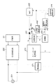
<給電制御系の構成>
図3は、本実施形態におけるレーザビームプリンタ100の給電制御系の構成を示す図である。商用電源301からの交流電圧は、定着器23に交番電流を供給する励磁回路(誘導加熱制御部)として機能する定着制御回路330と、スイッチング電源回路470とに供給されるような構成となっている。スイッチング電源回路470は、商用電源の交流電圧を画像形成部等で使用する24V等の直流電圧に降圧して供給している。電源回路470からの出力電圧Veは画像形成を制御する画像形成制御回路316を動作させるための電圧、出力電圧Vaは負荷460に電圧を供給している。ここで負荷460とは、発熱体としての励磁コイル506以外の画像形成部における負荷のことであり、例えば4つの感光体ドラム18a〜18dをそれぞれ個別に駆動する4つのDCブラシレスモータ(図示せず)、搬送ベルト20を駆動する1つのDCブラシレスモータ(図示せず)を含む。これらの計5個のDCブラシレスモータは、感光体ドラム18と当接したベルト20の表面が擦れないように、画像形成制御回路316により同時に回転駆動/停止の制御がなされる。また、これらのモータが駆動力を供給する感光体ドラム18a〜18d等は、レーザビームプリンタ100の使用し始めと耐久後でそのトルクが変動することが分かっているため、DCブラシレスモータのトルクや供給する電力も耐久後のトルクアップを見越して設計する必要がある。
<Configuration of power supply control system>
FIG. 3 is a diagram illustrating a configuration of a power supply control system of the
456は充電回路であり、スイッチング電源回路470から供給された電圧Vaを受け、画像形成制御回路316からの充電指令により、所定電圧Vb(ここではVb≒Va)を、例えば複数個の電気二重層コンデンサ素子で構成される蓄電器455に供給し、蓄電器455を所定電圧Vc(≒Vb)に充電するものである。電気二重層コンデンサは、その容量が数F以上と大きく、二次電池と比べて充電効率が良く、長寿命であるため近年多くの分野において注目されている素子である。
蓄電器455の充電電圧Vcは、蓄電器電圧検出回路457によって検出され、その検出結果は、例えばアナログ信号として画像形成制御回路316内にあるCPU(図示しない)のA/Dポートに送信される。画像形成制御回路316は、この蓄電器電圧検出回路457の検出結果に応じて充電回路456への充電要否の判断を行う。
The charging voltage Vc of the
定電圧制御回路458は例えばスイッチング方式の昇圧コンバータであり、蓄電器455の充電電圧Vcを負荷460の駆動に必要な電圧Vd(Vd≒Va−Vf,ただし、 Vd>Vc, Vf=ダイオード453の順方向電圧:約0.6V)に昇圧制御し、スイッチ463を介して負荷460に電圧Vdを供給し、モータの駆動等に用いられる。スイッチ463は、商用電源301または蓄電器455のいずれかを負荷460への電力供給源として選択する選択手段として機能する。すなわち、スイッチ463をオフにすれば、商用電源301が負荷460への電力供給源となり、逆にスイッチ463をオンにすれば、蓄電器455が負荷460への電力供給源となる。スイッチ463にはオンオフ耐久性の理由から、FET等の半導体スイッチを使用するのが好ましいものの、オンオフ回数などの寿命が問題なければリレー等のメカニカルスイッチを用いても構わない。また、ダイオード453は蓄電器455から定電圧制御回路458を介して電圧Vdを供給している際に、スイッチング電源回路470からの出力Vaが負荷460へ供給されないようにするものである。
The constant
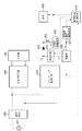
<定着制御回路330の構成>
まず、図4の定着器23の構成図を参照されたい。本実施形態では、同図に示すように、定着ベルト501の発熱域Sa(図7の発熱域Hに対応する)に対向する位置に温度検知素子としてのサーモスイッチ502を非接触で配設している。定着制御回路330は、例えば暴走時の励磁コイル506への給電を遮断すべく、このサーモスイッチ502の動作に応じて励磁コイル506への給電を制御する。ここではサーモスイッチ502のOFF動作温度を220℃に設定した。また、サーモスイッチ502と定着ベルト501との間の距離は略2mmとした。これにより、定着ベルト501にサーモスイッチ502の接触による傷が付くことがなく、耐久による定着画像の劣化を防止することができる。
<Configuration of Fixing
First, refer to the block diagram of the fixing
なお、この温度検知素子としては、サーモスイッチ502の代わりに温度ヒューズ等を用いてもよい。
As this temperature detection element, a temperature fuse or the like may be used instead of the
図9は、本実施形態における定着制御回路330の構成を示すブロック図である。この定着制御回路330は、サーモスイッチ502を+24VDC電源及びリレースイッチ303に直列に接続し、サーモスイッチ502が切れるとリレースイッチ303への給電が遮断されリレースイッチ303が動作し、定着制御回路330への給電が遮断されることにより励磁コイル506への給電を遮断する、という構成をとっている。
FIG. 9 is a block diagram showing a configuration of the fixing
図9に示した定着制御回路330の構成をその動作と共に詳述すると、整流回路304は、交流入力から両波整流を行うブリッジ整流回路と高周波フィルタを行うコンデンサで構成されている。第1および第2のスイッチ素子308,307はそれぞれ電流のスイッチングを行う。カレントトランス(CT)311は、第1および第2のスイッチ素子308、307でスイッチングされたスイッチング電流を検出するトランスである。
The configuration of the fixing
先述したとおり、定着器23には、励磁コイル506、温度検出サーミスタ405,406、過昇温を検出するサーモスイッチ502が設けられている。
As described above, the fixing
ゲートトランス306,305をそれぞれ介して第1および第2のスイッチ素子308,307を駆動するドライバ回路315は、カレントトランス311の出力電圧をフィルタリングするフィルタ325、発振回路328、コンパレータ等の比較器327、326で示される基準電圧Vs、クロック生成部329で構成される。クロック生成部329では、温調制御を行うためのクロックを生成すると共に、定着ベルト501と加圧ローラ530との相互圧接部の検出温度が規定温度を超過した場合に、画像形成制御部316からの信号により励磁コイル506への駆動パルスを停止し、定着器23への電力供給を停止する制御を行っている。
The
画像形成制御回路316は、定着器23に設けられているサーミスタ406の温度検出値に基づき、目標温度と比較しながら制御量をコントロールする。ドライバ回路315は、画像形成制御回路316からの制御信号を受けて、ゲートトランス305,306へのスイッチングクロックを生成し、高周波インバータ装置の制御形態に相応しい制御を行う。
The image
第1および第2のスイッチ素子308,307としては、パワー用電力スイッチ素子が最適であり、FETもしくはIGBT(+逆導通ダイオード)により構成されている。第1および第2のスイッチ素子308,307は共振電流を制御するため、定常時の損失及びスイッチ損失が小さいもので、なおかつ高耐圧、大電流タイプのものがよい。
As the first and
電源ライン入力端子301から交流入力電源を受け、リレー303を介して整流回路304に交流電源が印加されると、この整流回路304の両波整流ダイオードにより脈動化直流電圧が生成される。その後、第2のスイッチ素子307がスイッチングを行うようにゲート制御トランス305をドライブすることにより、励磁コイル506と共振コンデンサ309で構成された共振回路に交流パルス電圧が印加される。この結果、第1のスイッチ素子308の導通時には励磁コイル506に脈動化直流電圧が印加され、励磁コイル506のインダクタンスと抵抗により定まる電流が流れ始める。ゲート信号に従って第1のスイッチ素子308がターンオフすると、励磁コイル506は電流を流し続けようとするため、励磁コイル506の両端に共振コンデンサ309と励磁コイル506により定まる共振回路の尖鋭度Qによりフライバック電圧と呼ばれる高電圧が発生する。この電圧は電源電圧を中心に振動し、そのままオフ状態を保っておくと電源電圧に収束する。
When AC input power is received from the power
フライバック電圧のリンギングが大きく、第1のスイッチ素子308のコイル側端子の電圧が負になる期間は逆導通ダイオードがターンオフし、電流が励磁コイル506に流入する。この期間中、励磁コイル506と第1のスイッチ素子308の接点は0Vにクランプされることになる。このような期間に第1のスイッチ素子308をオンすれば、第1のスイッチ素子308は電圧を背負うことなくターンオン可能なことが一般に知られており、ZVS(Zero Voltage Switching)と呼ばれている。このような駆動方法により第1のスイッチ素子308のスイッチングに伴う損失を最小とすることができ、効率の良い、ノイズの少ないスイッチングが可能になる。
During a period in which the ringback of the flyback voltage is large and the voltage at the coil side terminal of the
次に、図9のカレントトランス311を用いた励磁コイル506の電流の検出について説明する。検出波形の一例を図10に示す。カレントトランス311は、第1のスイッチ素子308のエミッタ(FETの場合はドレイン)から整流回路304のマイナス端子及び整流回路304の後段のフィルタコンデンサ(図示略)へ流れる電流を検出すべく構成されている。1:nの巻線を有するカレントトランス311の1ターン側にパワー側の電流を流し、nターン側に設けた検出抵抗により電圧情報として検出する。スイッチング電流波形は図10のように、スイッチング周波数(20k〜500kHz)に対応した鋸歯状波を示しており、その電流ピーク値の包絡線は商用周波数(例えば50Hz)の正弦波を全波整流した形となっている。カレントトランス311で検出した検出電流はフィルタ325においてピークホールド整流される。フィルタ325でフィルタリングされた電流検出(電圧)値は比較器327の―入力端子へ、所定の基準電圧Vs326は比較器327の+入力端子へそれぞれ送信され、比較器327により双方の値を比較する。比較器327は、電流検出値が基準電圧Vs326よりも大きい場合には、基準電圧Vs326に対応する電流以上に大きなスイッチング(ピーク)電流が流れないように、ローレベルをクロック生成部329へ出力する。したがって、クロック生成部329からゲートトランス305,306へ送信されるクロックのオン時間が、パルスバイパルスで制限されスイッチング(ピーク)電流が制限される。
Next, detection of the current of the
図11は、図10に示したAの時間範囲について拡大表示したものである。この例では、第1のスイッチング素子 308を駆動するパルスのオン時間がtonaの場合、流れるスイッチング電流の検出電圧のピーク値は、所定電圧Vsに達していない。一方、定着器23への投入電力が増加した場合等において、オン時間がtonbとなった場合、この例では、流れるスイッチング電流の検出電圧のピーク値は、所定電圧Vsに達している。このため、クロック生成部329は、比較器327からの出力によりオン時間がtonbよりも長くならないように制限をかけている。つまり、スイッチング電流のピーク値を所定値に抑えることで、定着器23に投入される電力の最大電力を制限をするリミッタ動作を行う構成となっている。大電流が流れる場合等、異常電流検出時はこのような保護を行っている。
FIG. 11 is an enlarged view of the time range A shown in FIG. In this example, when the on-time of the pulse for driving the
次に、定着器23に投入される最大電力(初期電力)の電圧依存性について説明する。電流制御を全く行わない系においては、ACライン電圧に対し出力電力はACライン電圧の2乗で変動していくことになる。これに対し、電流検出によりリミットをかける本構成によれば、出力電力を入力電圧に線形依存するようにすることができる。
Next, the voltage dependence of the maximum power (initial power) input to the fixing
このような回路を構成し、実験を行った結果を図12に示す。図12の「制御無し領域」は、電流制御を行わない場合の実験結果であり、入力電圧の2乗で電力変化がみられ、電源電圧による電力依存性が大きい。一方、「ピーク一定制御領域」は、レーザビームプリンタ100に用いられる電圧を含む入力電圧範囲内において、検出したピーク電流が一定になるよう制御した場合の実験結果である。図より、電源電圧による電力変動が少ないことを示している。つまり、検出したピーク電流に基づいて電力制御回路の最大出力値を制御することにより、ACライン電流検出結果により電力制御幅の最大値(最大投入可能電力)を制御し、最大供給可能な電力がACライン電圧に依存し難くなるよう制御している。
FIG. 12 shows the result of an experiment conducted with such a circuit. The “non-control region” in FIG. 12 is an experimental result when current control is not performed, and a power change is observed with the square of the input voltage, and power dependency due to the power supply voltage is large. On the other hand, the “constant peak control region” is an experimental result when the detected peak current is controlled to be constant within the input voltage range including the voltage used in the
電流を検出し電力を制御するということから、定着器23の励磁コイル506に電流を流す時間、即ち第1のスイッチ素子308のオンしている時間の最大値はACラインを流れる電流と供給可能な電力により定め、画像形成制御回路316からの制御信号はその時間を超えない範囲となっている。また、最小時間についても規定する構成をとってもよい。
Since the current is detected and the electric power is controlled, the maximum value of the time during which the current flows through the
<電力制御動作>
以下では本実施形態における電力制御について説明する。
<Power control operation>
Below, the power control in this embodiment is demonstrated.
画像形成装置は一般に大電力を消費する。その電力消費の多くは、定着器によるものである。そこで、動作モードとして、プリント要求の待機状態が一定時間以上続いた場合に、定着器への供給電力を落として待機するいわゆる省エネルギーモードあるいはスリープモードに移行する、という電力制御が行われるのが一般的である。本実施形態におけるレーザビームプリンタ100も、動作モードとしてこの省エネルギーモードを有している。省エネルギーモードでは当然、定着器の温度は下がる。そうすると、電源スイッチ投入時だけでなく、省エネルギーモードから復帰する時(通常モードに移行する時)にも、定着器が冷えていると考えられる。定着器が冷えた状態からスタンバイ状態の温度に達するまでの時間(ウォームアップ時間)を短縮することが課題となっていることは先述したとおりであるが、この課題は以下に説明する本実施形態の電力制御によって解決される。
An image forming apparatus generally consumes a large amount of power. Much of its power consumption is due to the fuser. Therefore, as an operation mode, when the standby state for a print request continues for a certain time or more, power control is generally performed such that the power supply to the fixing device is reduced to shift to a so-called energy saving mode or sleep mode. Is. The
画像形成制御回路316は、まず、省エネルギーモード時あるいは蓄電器455からの電力供給が不要な時は、スイッチ463をオフにするとともに、充電回路456を動作させて蓄電器455を充電しておく。
First, the image
一方、電源投入時または省エネルギーモードからの復帰時あるいはプリント要求を受けた時、画像形成動作開始時等の定着器23を使用する際には、画像形成制御回路316は、スイッチ463をオンにして、蓄電器455からの電力により負荷460を駆動する。したがって、蓄電器455からの電力供給により負荷460で消費する電力分が、商用電源から消費されなくなるため、商用電源の最大電流から規定される最大電力に対して余力ができることになる。
On the other hand, when the fixing
例えば、定着器23の温度立上げ時において、定着制御回路330の一次側(AC側)で11Aの電流が流れており、スイッチング電源回路470の一次側(AC側)で3Aの電流が流れているとする。定着制御回路330での入力電圧に依存する電力等のバラツキを約1A見込むと、その合計電力は、(定着制御回路330とスイッチング電源回路470の力率cosθが共に1であると仮定すると、)15A(=11A+3A+1A)となり、商用電源の最大電流15A以内、つまり許容電力1500W(=100V×15A)内に収まる。
For example, when the temperature of the fixing
このような条件の下、蓄電器455から負荷460への電力供給により、スイッチング電源回路470の一次側(AC側)での電流値が2A軽減したとすると、蓄電器455からの電力により負荷460を駆動している間、この2A分の電力(200W=100V×2A)が商用電源から消費されなくなるため、商用電源の最大供給電流に対して余力ができることになる。このため、画像形成制御回路316は、定着制御回路330のドライバ315内の基準電圧Vs326をこの2Aに相当する分上昇させ、定着器23への投入電力制限値を高くする。したがって、定着制御回路330の一次側(AC側)で13A、スイッチング電源回路470の一次側(AC側)で1A、バラツキは変わらず約1Aであり、その合計電流は同様に15A(=13A+1A+1A)で、商用電源の最大許容電力内に収まる。なお、当然のことながら、実際の設計時には設計バラツキを考慮して、商用電源の最大供給可能な電流を超えないようにしておく必要がある。
Under such conditions, if the current value on the primary side (AC side) of the switching
このように、蓄電器455から負荷460への給電状態、すなわち、選択手段としてのスイッチ463の状態、に応じて基準電圧Vs326を調整することにより、定着器23への投入電力制限レベルを調整することができる。
In this way, by adjusting the
また、上記のように蓄電器455を用いることにより、定着器23の温度立ち上げ時において約200W(=100V×2A)の電力を定着器23へ供給することが可能な場合には、オンデマンド定着を実現できる可能性が出てくる。すなわち、図27において、上記同様に蓄電器455の利用により200Wの電力を定着器23へさらに供給することで、図中のプリント温度までに達する時間が30sec(点Wa)が15sec (点Wb)となり、定着器23の温度立ち上げ時間を短縮することが可能となる。
In addition, when the
本実施形態における電力制御動作は概ね上記のとおりであるが、以下では、さらに蓄電器455の充電状態および/または定着器23の温度を加味した電力制御について説明する。
The power control operation in the present embodiment is generally as described above. Hereinafter, power control that further considers the state of charge of the
図23は、画像形成制御回路316による、蓄電器455の充電状態および/または定着器23の温度を加味した電力制御の動作を示すフローチャートである。本処理は、電源投入時または省エネルギーモードから復帰した時に開始する。
FIG. 23 is a flowchart showing the power control operation by the image
まずステップS401で、画像形成制御回路316は、定着器23に設けられているサーミスタ406の温度検出値を入力し(図9を参照)、その温度検出値が定着可能な下限の温度TL以上である否かを判断する。定着器23の温度が既に定着可能な下限の温度TL以上ある場合にはそもそも蓄電器455から電力を供給して定着器23の急速立ち上げを行う必要はないので、ステップS407に進み、スイッチ463のオフ状態を維持することで商用電源301から通常の電力WLを定着器23に供給する。続くステップS408はスイッチ463をオフすることで蓄電器455を負荷460から切断する処理であるが、この場合には元々スイッチ463はオフ状態に維持されているので、そのまま本処理を終了する。
First, in step S401, the image
一方、ステップS401で、サーミスタ406の温度検出値(すなわち定着器23の温度)がTL未満の場合には、ステップS402に進み、蓄電器電圧検出回路457によって検出される蓄電器455の充電電圧Vcが、定電圧制御回路458が負荷460の駆動に必要な電圧Vdにまで昇圧可能な下限の電圧VL以上であるか否かを判断する。ここで、蓄電器455の充電電圧VcがVLに満たない場合は、充電が不十分であるとみなして、上記ステップS401で定着器23の温度が既に定着可能な下限の温度TL以上ある場合と同様にステップS407に進む。この充電が不十分なままスイッチ463のオンして蓄電器455からの電力を供給しても、定着器23の急速立ち上げに寄与しないばかりか、かえってその立ち上げに支障をきたすおそれもあるからである。
On the other hand, if the temperature detection value of the thermistor 406 (that is, the temperature of the fixing device 23) is less than TL in step S401, the process proceeds to step S402, where the charging voltage Vc of the
ステップS402において、充電電圧VcがVL以上ある場合には、ステップS403に進み、蓄電器404を負荷460に接続すべく、スイッチ463をオンする。したがって、負荷460は蓄電器455からの電力によって駆動することになる。これにより、商用電源の最大電流から規定される最大電力に対して余力ができ、その余力を定着器23に回すことが可能になることを先述したとおりである。
If the charge voltage Vc is equal to or higher than VL in step S402, the process proceeds to step S403, and the
そこで本実施形態では、ステップS404において、定着器23への供給電力を、上記商用電源の最大電力に対する余力の電力WFだけ増加させる。具体的には、例えば、定着制御回路330のドライバ315内の基準電圧Vs326(図9を参照)を、電力WFに相当する分上昇させ、定着器23への投入電力制限値を高くすることで実現できる。これにより、定着器23に供給される電力は、商用電源301からの通常の電力WL+WFとなる。なお、このとき定着器23に供給される電力(WL+WF)は、商用電源301の電圧範囲内での最低電圧(例えば、電圧範囲を100〜127Vとすると、その下限電圧である100V)に合わせて設定するのが望ましい。
In this embodiment, in step S404, the power supplied to the
上記のステップS403,S404によって蓄電器455からの電力が負荷460に供給されている間は、ステップS405およびS406でそれぞれ、蓄電器電圧検出回路457によって検出される蓄電器455の充電電圧Vcが、定電圧制御回路458が負荷460の駆動に必要な電圧Vdにまで昇圧可能な下限の電圧VL以上に維持されているかどうか、および、サーミスタ406の温度検出値が、定着器23が定着可能な下限の温度TL以上になったかどうか、を監視している。
While the electric power from the
ここで、蓄電器455の充電電圧VcがVLを下回ったとき(ステップS405→NO)、または、サーミスタ406の温度検出値(すなわち、定着器23の温度)がTL以上になったとき(ステップS406→YES)は、ステップS407に進み、定着器23への供給電力を、通常電力WLに戻す。具体的には、例えば、定着制御回路330のドライバ315内の基準電圧Vs326(図9を参照)を、ステップS404で増加した電力WFに相当する分降下させ、定着器23への投入電力制限値を低くすることで実現できる。
Here, when the charging voltage Vc of the
そして、ステップS408で、スイッチ463をオフすることで蓄電器455を負荷460から切断し、本処理を終了する。
In step S408, the
以上説明した蓄電器455の充電状態および/または定着器23の温度を加味した電力制御の効果を説明する。図26は、本実施形態と、蓄電器を使用しない従来例のそれぞれについて、定着器への電力供給量の時間推移を示している。同図中、(B)の実線aは、本実施形態における定着器23への電力供給量を示しており、(C)の破線bは、蓄電器を使用しない従来例における定着器への電力供給量を示している。また、(A)の実線c、dはそれぞれ、定着器への電力供給に伴う、本実施形態の定着器の温度の時間遷移、従来の定着器の温度の時間遷移を示している。
The effect of power control taking into account the state of charge of the
同図に示すように、定着器が定着可能な下限の温度TLよりも低い温度から立ち上げる場合、従来の画像形成装置では、定着器に商用電源の通常電力WLだけを供給し、その定着器の温度がTLに達するまでに時間t2を要していたところ、本実施形態のレーザビームプリンタ100においては、定着器23への電力供給量をWFだけ増加させているので、その定着器の温度がTLに達するまでの時間は、t2より短いt1で済む。
As shown in the figure, when the fixing device is started up from a temperature lower than the temperature T L of the fixable lower limit, in the conventional image forming apparatus supplies only the normal power W L from the commercial power source to a fixing device, the When the temperature of the fuser has required time t 2 to reach T L, the
なお、上述の充電状態および/または定着器の温度を加味した電力制御では、ステップS406のように、蓄電器455を負荷460から切断する条件を、定着器23の温度が定着可能な下限の温度を下回ったこと、としたが、定着器23への供給電力、上昇温度および降下温度と時間の関係が予め分かっている場合には、ステップS406のような条件の代わりに、経過時間あるいは総供給電力量で設定することも可能である。
In the power control that takes into account the charging state and / or the temperature of the fixing device, the condition for disconnecting the
以上のように、レーザビームプリンタ100内に蓄電器455を設け、定着起動時に蓄電器455から、定着器23以外のモータ等の負荷460に電力を供給することで、蓄電器455からの電力供給が行われている間、余剰電力に相当する分、定着器23への電力制限値を増加させることが可能となり、その余剰電力を定着器23の立上げ電力として有効活用することで、定着器23の立上げ時間を短縮することができる。また、定着器23内には、主ヒータ、副ヒータといった複数の熱源を必要としないため定着器の構成を簡素化することができるとともに、画像形成装置の構成や印字速度等の性能によってはオンデマンド定着の実現が可能となる。
As described above, the
以上、本発明の第1の実施形態を説明した。以下では、別の実施形態をいくつか説明する。それぞれ、画像形成装置の概略構成をはじめ各部の構成および動作も上述した第1の実施形態と概ね同様であるが、給電制御系の構成に特徴的な違いを呈するものである。そこで以下の実施形態では、第1の実施形態で用いた図面を援用すると共に、新たに用いる図面については、第1の実施形態と共通する構成には同一の参照番号を付してそれらの説明は省略し、他の実施形態と相違する構成または動作について説明することにする。 The first embodiment of the present invention has been described above. In the following, several other embodiments will be described. The configuration and operation of each part including the schematic configuration of the image forming apparatus are substantially the same as those of the first embodiment described above, but the characteristic differences in the configuration of the power supply control system are exhibited. Therefore, in the following embodiment, the drawings used in the first embodiment are used, and for the newly used drawings, the same reference numerals are assigned to the same components as those in the first embodiment, and the descriptions thereof are made. Is omitted, and a configuration or operation different from that of the other embodiments will be described.
■ 第2の実施形態 ■
図13は、第2の実施形態におけるレーザビームプリンタ100の給電制御系の構成を示す図である。第1の実施形態(図3)との違いは、スイッチング電源回路470の入力側(一次側)に電流検出回路471を設けている点である。この電流検出回路471で検出される電流は、商用電源301から負荷460に供給される電力に対応する物理量である。
■ Second Embodiment ■
FIG. 13 is a diagram illustrating a configuration of a power supply control system of the
電流検出回路471は、スイッチング電源回路470へ流れる入力電流の実効値あるいは平均値を検出し、その検出値を例えばアナログ信号として画像形成制御回路316内にあるCPU(図示せず)のA/Dポートに送信する。
The
画像形成制御回路316は、電流検出回路471の電流検出結果に応じて、定着制御回路330の基準電圧Vs326(図9)を変更し、電力制限値を所定の値に変更する。
The image
たとえば、第1の実施形態では、負荷460のバラツキや経年変化等を考慮し、負荷460が消費する最大の消費電力を考慮して電力制限値の変更度合いを決めておく必要がある。しかしながら、通常この想定し得る最大消費電力となることは稀で、画像形成動作時においては、想定した最大消費電力よりも十分低い消費電力となっている。この最大消費電力と実際の消費電力に差がある場合には、その差の電力が余剰電力と考えられる。したがって、スイッチ463が閉じていて蓄電器455から負荷460へ電力が供給されている時、電流検出回路471で検出した電流検出結果より、想定した最大消費電力と負荷460で消費している実際の電力の差を算出し、その余力電力分を定着制御回路330の電力制限値をさらに大きな値として設定することが可能となる。また、電流検出回路471の検出信号はアナログ信号のため、そのアナログ値に応じた、電力制限値をデータテーブルとしてあらかじめ用意しておけば、画像形成制御回路316はそのテーブルを参照することで、定着への電力制限値を選択することが可能となる。
For example, in the first embodiment, it is necessary to determine the degree of change in the power limit value in consideration of the maximum power consumption consumed by the
以上のことから、負荷460で消費している電力が少ない時(モータトルクが小さい時に)、負荷460での消費電力が小さいほど定着器23へ電力を供給することが可能となるため、定着器23の起動時(電力投入時)においてさらに最適な電力供給が可能となる。
From the above, when the power consumed by the
図14は、本実施形態における変形例として、スイッチング電源回路470の入力側(一次側)に、電流検出回路471を設ける代わりに、商用電源301の電圧を検出する電圧検出回路482を設けた例を示している。この電圧検出回路482で検出される電圧は、商用電源301から負荷460に供給される電力に対応する物理量である。
FIG. 14 shows an example in which a
電圧検出回路482は、商用電源301の電圧の実効値あるいは平均値を検出し、その検出値を例えばアナログ信号として画像形成制御回路316内にあるCPU(図示せず)のA/Dポートに送信する。画像形成制御回路316は電圧検出回路482の電圧検出結果に応じて、定着制御回路330の基準電圧Vs326(図9)を変更し、電力制限値を所定の値に変更する。
The
このレーザビームプリンタ100が使用される国の規格によるものの、商用電源301の限界電力は一般に電流値で規定されているため、仮に15Aまで供給可能な商用電源があるとすると、その商用電源電圧値が大きくなればなるほど大きな電力が供給可能となる。さらに、スイッチング電源の入力側(一次側)に流れる電流は、二次側で消費する電力が一定であるとすると、入力電圧が低いほど大きくなるため、定着器側へ供給できる電流(電力)が減少してしまう。
Although the limit power of the
したがって、第1の実施形態のように入力電圧を検出する手段を持たない構成においては、定着器23での電力制限値を決定する上でのパラメータとして考えられる(1)入力電圧範囲における商用電源の最大供給可能電流(電力)、および、(2)入力電圧変化に対するスイッチング電源での電流変化、を加味し、入力電圧範囲内において、商用電源から供給可能な最大電流値を超えないように、定着制御回路330での電力制限値を設定しておく必要がある。つまり、入力電圧によっては商用電源の最大供給可能電流(電力)に対して十分余力のある制御となっている。
Therefore, in the configuration having no means for detecting the input voltage as in the first embodiment, it can be considered as a parameter for determining the power limit value in the fixing
図14のように、電圧検出回路482を設け、入力電圧(商用電源電圧)を検知するような構成とすれば、検出した入力電圧のアナログ値と上記(1),(2)のパラメータにそれぞれ対応した、最適な定着電力制限値をデータテーブルをあらかじめ設けておくことができる。したがって、電圧検出回路482で検出した入力電圧(商用電源電圧)の検出結果を基に、テーブルを参照することで、入力電圧の変動に左右されずに、定着器23の起動時(電力投入時)においてさらに最適な電力供給が可能となる。
As shown in FIG. 14, if the
以下、この図14に示した構成をベースにした電力制御の一例を説明する。 Hereinafter, an example of power control based on the configuration shown in FIG. 14 will be described.
図24は、本実施形態における画像形成制御回路316による電力制御動作を示すフローチャートである。本処理は、電源投入時または省エネルギーモードからの復帰時に開始する。
FIG. 24 is a flowchart showing a power control operation by the image
まずステップS701で、画像形成制御回路316は、定着器23に設けられているサーミスタ406の温度検出値を入力し(図9を参照)、その温度検出値が定着可能な下限の温度TL以上である否かを判断する。定着器23の温度が既に定着可能な下限の温度TL以上ある場合にはそもそも蓄電器455から電力を供給して定着器23の急速立ち上げを行う必要はないので、ステップS708に進み、スイッチ463のオフ状態を維持することで商用電源301から通常の電力WLを定着器23に供給する。続くステップS709はスイッチ463をオフすることで蓄電器455を負荷460から切断する処理であるが、この場合には元々スイッチ463はオフ状態に維持されているので、そのまま本処理を終了する。
First, in step S701, the image
一方、ステップS701で、サーミスタ406の温度検出値(すなわち、定着器23の温度)がTL未満の場合には、ステップS702に進み、蓄電器電圧検出回路457によって検出される蓄電器455の充電電圧Vcが、定電圧制御回路458が負荷460の駆動に必要な電圧Vdにまで昇圧可能な下限の電圧VL以上であるか否かを判断する。ここで、蓄電器455の充電電圧VcがVLに満たない場合は、充電が不十分であるとみなして、上記ステップS701で定着器23の温度が既に定着可能な下限の温度TL以上ある場合と同様にステップS708に進む。
On the other hand, if the temperature detection value of the thermistor 406 (that is, the temperature of the fixing device 23) is less than T L in step S701, the process proceeds to step S702, and the charging voltage Vc of the
ステップS702において、充電電圧VcがVL以上ある場合には、ステップS703に進み、蓄電器404を負荷460に接続すべく、スイッチ463をオンする。したがって、負荷460は蓄電器455からの電力によって駆動することになる。
In step S702, when the charging voltage Vc is equal to or higher than VL , the process proceeds to step S703, and the
次に、ステップS704において、画像形成制御回路316は電圧検出回路482により検出される商用電源電圧を入力する。画像形成制御回路316は、商用電源301の電圧と定着器23へ供給する電力増加分との対応関係を記述したテーブルを、例えば画像形成制御回路316内の図示しないメモリ内にあらかじめ記憶しておく。例えばそのテーブルには、所定の電圧範囲内(例えば、100〜127V)のV1〜Vnに対応した、定着器23に供給する電力増加分W1〜Wnが記述されている。ステップS705では、このテーブルを参照して、定着器23に供給する電力を、ステップS704で検出された商用電源電圧Vx(Vx=V1, V2, V3 … Vn)に対応する電力Wx(Wx=W1, W2, W3 … Wn)だけ増加させる。具体的には、例えば、定着制御回路330のドライバ315内の基準電圧Vs326(図9を参照)を、電力Wxに相当する分上昇させ、定着器23への投入電力制限値を高くすることで実現できる。
In step S <b> 704, the image
上記のステップS703〜S705によって蓄電器455からの電力が負荷460に供給されている間は、ステップS706およびS707でそれぞれ、蓄電器電圧検出回路457によって検出される蓄電器455の充電電圧Vcが、定電圧制御回路458が負荷460の駆動に必要な電圧Vdにまで昇圧可能な下限の電圧VL以上に維持されているかどうか、および、サーミスタ406の温度検出値が、定着器23が定着可能な下限の温度TL以上になったかどうか、を監視している。
While the electric power from the
ここで、蓄電器455の充電電圧VcがVLを下回ったとき(ステップS706→NO)、または、サーミスタ406の温度検出値(すなわち、定着器23の温度)がTL以上になったとき(ステップS707→YES)は、ステップS708に進み、定着器23への供給電力を、通常電力に戻す。具体的には、例えば、定着制御回路330のドライバ315内の基準電圧Vs326(図9を参照)を、ステップS705で増加した電力Wxに相当する分降下させ、定着器23への投入電力制限値を低くすることで実現できる。
Here, when the charging voltage Vc of the
そして、ステップS709で、スイッチ463をオフすることで蓄電器455を負荷460から切断し、本処理を終了する。
In step S709, the
図15は、本実施形態における別の変形例として、スイッチング電源回路470の入力側(一次側)に、電流検出回路471を設ける代わりに、商用電源301から負荷460に供給される電力を検出する電力検出回路483を設けた例を示している。
FIG. 15 shows, as another modification of the present embodiment, the power supplied from the
電力検出回路483は、スイッチング電源回路470の入力側(一次側)で電力の実効値あるいは平均値を検出し、その検出値を例えばアナログ信号として画像形成制御回路316内にあるCPU(図示せず)のA/Dポートに送信する。画像形成制御回路316は、蓄電器455からの電力供給時において、電力検出回路483の電力検出結果に応じて、定着制御回路330の基準電圧Vs326(図9)を変更し、電力制限値を所定の値に変更する。
The
なお、電力検出回路483を設ける代わりに、前述の電流検出回路471と電圧検出回路483の双方を設け、それぞれ検出した電流値と電圧値とから画像形成制御回路内316において演算により電力を求めてもよい。
Instead of providing the
スイッチング電源回路470の入力側電力に応じた電力制限値をデータテーブルとしてあらかじめ用意しておけば、画像形成制御回路316は電力検出回路483で検出した電力値を基に、その電力値に対応するテーブル上の制限値を参照することで、定着への電力制限値を選択することが可能となる。
If a power limit value corresponding to the input side power of the switching
■ 第3の実施形態 ■
図16は、第3の実施形態におけるレーザビームプリンタ100の給電制御系の構成を示す図である。第2の実施形態における第3の変形例(図15)との違いは、電力検出回路484を、スイッチング電源回路470の入力側(一次側)ではなく、定着制御回路330の入力側に設けた点である。この電力検出回路484で検出される電力は、商用電源301から定着器23に供給される電力である。
■ Third Embodiment ■
FIG. 16 is a diagram illustrating a configuration of a power supply control system of the
電力検出回路484は、定着制御回路330の入力側(一次側)電力の実効値あるいは平均値を検出し、その検出値を例えばアナログ信号として画像形成制御回路316内にあるCPU(図示せず)のA/Dポートに送信する。画像形成制御回路316は、蓄電器455からの電力供給時において、電力検出回路484の電力検出結果に応じて、定着制御回路330の基準電圧Vs326(図9)を変更し、電力制限値を所定の値に変更する。
The
なお、電力検出回路484を設ける代わりに、図14に示した電圧検出回路482を設けてこれにより電圧値を検出し、この電圧値と、カレントトランス311により検出されるスイッチング電流値とから、画像形成制御回路内316において演算により電力を求めてもよい。
Instead of providing the
また、定着制御回路330の入力側電力に応じた電力制限値をデータテーブルとしてあらかじめ用意しておけば、画像形成制御回路316は電力検出回路484で検出した電力値を基に、その電力値に対応するテーブル上の制限値を参照することで、定着への電力制限値を選択することが可能となる。
If a power limit value corresponding to the input side power of the fixing
■ 第4の実施形態 ■
図17は、第4の実施形態におけるレーザビームプリンタ100の給電制御系の構成を示す図である。第2の実施形態(図13)との違いは、電流検出回路485を、スイッチング電源回路470の入力側(一次側)への分岐点の前段に設け、商用電源301の電流を検出するようにした点である。この電流検出回路485で検出される電流は、商用電源301の電力に対応する物理量である。
■ Fourth embodiment ■
FIG. 17 is a diagram illustrating a configuration of a power supply control system of the
電流検出回路485は、商用電源301に流れる入力電流の実効値あるいは平均値を検出し、その検出値を例えばアナログ信号として画像家製制御回路316内にあるCPU(図示せず)のA/Dポートに送信する。画像形成制御回路316は、電流検出回路485の電流検出結果に応じて、定着制御回路330の基準電圧Vs326(図9)を変更し、電力制限値を所定の値に変更する。
The
このレーザビームプリンタ100が使用される国の規格によるものの、商用電源301の限界電力は一般に電流値で規定されているため、仮に15Aまで供給可能な商用電源があるとすると、その商用電源電圧値が大きくなればなるほど大きな電力が供給可能となる。つまり、本実施形態のように商用電源301に流れる電流を電流検出回路485により検出することで、より最適な定着電力制御が可能になる。
Although the limit power of the
画像形成制御回路316は、電流検出回路485により検出した電流値をリアルタイムでモニタしながら、検出電流の最大電流値が商用電源301で供給可能な電流15A以内に収まるようにリアルタイムで定着電力制限値をコントロールする。すなわち、定着立上げ時においては、スイッチ463をオンし蓄電器455から負荷460へ電力供給すると共に、最大電流値が15Aを超えないような所定の電力制限値を設定する。電流検出回路485により検出した最大電流値と商用電源301から供給可能な電流(電力)の上限値15Aとの差に相当する電力分定着電力制限値を上昇させる。したがって、最適な定着電力制御が可能となっている。
The image
図25は、本実施形態における画像形成制御回路316による電力制御動作を示すフローチャートである。本処理は、電源投入時または省エネルギーモードからの復帰時に開始する。
FIG. 25 is a flowchart showing a power control operation by the image
まずステップS901で、画像形成制御回路316は、定着器23に設けられているサーミスタ406の温度検出値を入力し(図9を参照)、その温度検出値が定着可能な下限の温度TL以上である否かを判断する。定着器23の温度が既に定着可能な下限の温度TL以上ある場合にはそもそも蓄電器455から電力を供給して定着器23の急速立ち上げを行う必要はないので、ステップS908に進み、スイッチ463のオフ状態を維持することで商用電源301から通常の電力WLを定着器23に供給する。続くステップS909はスイッチ463をオフすることで蓄電器455を負荷460から切断する処理であるが、この場合には元々スイッチ463はオフ状態に維持されているので、そのまま本処理を終了する。
First, in step S901, the image
一方、ステップS901で、サーミスタ406の温度検出値(定着器23の温度)がTL未満の場合には、ステップS902に進み、蓄電器電圧検出回路457によって検出される蓄電器455の充電電圧Vcが、定電圧制御回路458が負荷460の駆動に必要な電圧Vdにまで昇圧可能な下限の電圧VL以上であるか否かを判断する。ここで、蓄電器455の充電電圧VcがVLに満たない場合は、充電が不十分であるとみなして、上記ステップS901で定着器23の温度が既に定着可能な下限の温度TL以上ある場合と同様にステップS908に進む。
On the other hand, if the temperature detection value of the thermistor 406 (the temperature of the fixing device 23) is less than TL in step S901, the process proceeds to step S902, where the charging voltage Vc of the
ステップS902において、充電電圧VcがVL以上ある場合には、ステップS903に進み、蓄電器404を負荷460に接続すべく、スイッチ463をオンする。したがって、負荷460は蓄電器455からの電力によって駆動することになる。
In step S902, when the charging voltage Vc is equal to or higher than VL , the process proceeds to step S903, and the
次に、ステップS904で、画像形成制御回路316は電流検出回路485により検出される商用電源301からの電流Ipを入力し、この電流Ipが商用電源301の上限電流値Imax(例えば15A)未満となっているかを監視する。電流IpがImaxを下回っていることが確認されると、ステップS905に進み、定着器23への供給電力を、δWだけ増加させる。具体的には、例えば、定着制御回路330のドライバ315内の基準電圧Vs326(図9を参照)を、電力δWに相当する分上昇させ、定着器23への投入電力制限値を高くすることで実現できる。これにより、定着器23に供給される電力は、商用電源301からの通常の電力WL+δWとなる。その後、ステップS907に進み、サーミスタ406の温度検出値が、定着器23が定着可能な下限の温度TL以上になったかどうか、をチェックする。ここで、サーミスタ406の温度検出値がTL未満であるとき(ステップS907→NO)は、ステップS904に戻って処理を繰り返す。
Next, in step S904, the image forming
上記のステップS904→S905→S907の処理ループをx回繰り返すと、定着器23への供給電力は商用電源301からの通常の電力WLよりもx・δw増加することになる。この処理ループをx回繰り返すことによって、ステップS904において、Ip<Imaxの条件を満たさなくなった場合には、ステップS906に進み、定着器23への供給電力をWL+x・δWに維持して、ステップS907に進む。
Repeating the processing loop of steps S904 → S905 → S907 x times, the power supplied to the
ステップS907で、サーミスタ406の温度検出値がTL以上になったとき(ステップS907→YES)は、ステップS908に進み、定着器23への供給電力を、通常電力WLに戻す。具体的には、例えば、定着制御回路330のドライバ315内の基準電圧Vs326(図9を参照)を、ステップS905〜S907のループをx回繰り返したことによる電力増加分x・δWに相当する分降下させ、定着器23への投入電力制限値を低くすることで実現できる。
In step S907, when the detected temperature of the
そして、ステップS909で、スイッチ463をオフすることで蓄電器455を負荷460から切断し、本処理を終了する。
In step S909, the
以上のような電力制御によれば、商用電源301の電流Ipを検出し、その検出結果に応じて定着器23への供給電力が制御される。これにより、蓄電器455から負荷460へ供給される電力に依存することなく商用電源を効率よく利用できるため、より速く定着器23を定着可能な状態に立ち上げることができる。
According to the power control as described above, the current I p of the
上記の電力制御の例では、蓄電器455の電圧を検出するステップは示さなかったが、所定のタイミングで蓄電器455の電圧を検出するようにすれば、蓄電器455の容量が減少し出力が急激に低下したときや、蓄電器455に障害が発生した場合に、IpがImaxを超えることがないように容易に制御できるようになるので、より好ましい。
In the above power control example, the step of detecting the voltage of the
図18は、本実施形態における変形例として、スイッチング電源回路470の入力側(一次側)への分岐点の前段に、電流検出回路485の代わりに、電力検出回路486を設け、商用電源301の電力を検出するようにした例を示している。
FIG. 18 shows, as a modification of the present embodiment, a
電力検出回路486は、定着制御回路330の入力側(一次側)電力の実効値あるいは平均値を検出し、その検出値を例えばアナログ信号として画像形成制御回路316内にあるCPU(図示せず)のA/Dポートに送信する。画像形成制御回路316は、電力検出回路486の電力検出結果に応じて、定着制御回路330の基準電圧Vs326(図9)を変更し、電力制限値を所定の値に変更する。
The
なお、電力検出回路486を設ける代わりに、前述の電流検出回路485と電圧検出回路482の双方を設け、それぞれ検出した電流値と電圧値から画像形成制御回路内316において演算により電力を求めてもよい。
Instead of providing the
また、定着制御回路330の入力側電力に応じた電力制限値をデータテーブルとしてあらかじめ用意しておけば、画像形成制御回路316は電力検出回路486で検出した電力値を基に、その電力値に対応するテーブル上の制限値を参照することで、定着への電力制限値を選択することが可能となる。
If a power limit value corresponding to the input side power of the fixing
■ 第5の実施形態 ■
上述の各実施形態では、電磁誘導加熱方式の定着器23を使用したが、その他の方式の定着器を使用することも可能である。本実施形態では、セラミック面状発熱ヒータ方式の定着器について説明する。
■ Fifth Embodiment ■
In each of the above-described embodiments, the electromagnetic induction heating
図19は、本実施形態におけるセラミック面状発熱ヒータ方式の定着器600の横断面構造を示す図である。
FIG. 19 is a diagram showing a cross-sectional structure of a ceramic sheet heating heater
610はステーであり、このステー610はセラミックヒータ640を露呈させて支持した横断面U字状の本体部611と該本体部を対向する加圧ローラ620側へ加圧する加圧部613とで構成されている。ここで、セラミック面状発熱ヒータは、発熱体が後述のニップ部と反対側であっても、発熱体がニップ部側であっても構わない。614はステー610に外嵌させてある横断面円形の耐熱性フィルム(以下、「フィルム」と略称する)である。
加圧ローラ620は、セラミックヒータ640との間にフィルム614を挟んで圧接ニップ部(定着ニップ部)Nを形成し、且つフィルム614を回転駆動させるフィルム外面接触駆動手段として作用する。このフィルム駆動ローラ兼加圧ローラ620は芯金620aとシリコンゴム等よりなる弾性体層620bと最外層の離形層620cよりなり、不図示の軸受け手段・付勢手段により所定の押圧力をもってフィルム614を挟ませてセラミックヒータ640の表面に圧接させて配設してある。この加圧ローラ620はモータMによる回転駆動により、この加圧ローラ620とフィルム614の外面との摩擦力で該フィルムに搬送力を付与する。
The
図20は、セラミック面状発熱ヒータ640の具体的な構造例を示す図である。図20(a)はセラミック面状発熱ヒータ640の断面図であり、図20(b)は発熱体601が形成されている面を示している。
FIG. 20 is a diagram showing a specific structure example of the
セラミック面状発熱ヒータはSiC、AlN、Al2O3等のセラミックス系の絶縁基板607と絶縁基板面上にペースト印刷等で形成されている発熱体601と、発熱体保護しているガラス等の保護層606から構成されている。保護層上には、セラミック面状発熱ヒータの温度を検出する温度検出素子としてのサーミスタ605および過昇温を防止する手段として例えば温度ヒューズ602が配置されている。サーミスタ605は発熱体601に対して絶縁距離を確保できるように絶縁耐圧を有する絶縁物を介して配置されている。もっとも、過昇温を防止する手段としては温度ヒューズの他にサーモスイッチ等を使用してもよい。
The ceramic sheet heater is composed of a ceramic insulating
発熱体601は、電力が供給されると発熱する部分と、その発熱部分に接続した導電部603と、コネクタを介して電力が供給される電極部604とから構成され、発熱部601は通紙可能な最大の記録紙幅LFとほぼ同じ長さとしている。2つの電極604のうち1つへは、交流電源のHOT側端子が温度ヒューズ602を介して接続されている。電極部は発熱体を制御するトライアック639に接続され、交流電源のNEUTRAL端子に接続される。
The
図21は、本実施形態における定着制御回路630の構成を示す図である。この定着制御回路630はセラミック面状発熱ヒータ方式によるものであるが、図3では定着制御回路330と置き換えることができるものである。
FIG. 21 is a diagram showing a configuration of the fixing
本実施形態におけるレーザビームプリンタ100は、商用電源301をACフィルタ(図示せず)を介してセラミック面状発熱ヒータ640の発熱体601へ供給することによりセラミック面状発熱ヒータの発熱体601を発熱させる。この発熱体601への電力供給は、トライアック639によって通電・遮断が制御される。抵抗631,632はトライアック639のためのバイアス抵抗であり、フォトトライアックカプラ633は一次、二次間を隔離するためのデバイスである。フォトトライアックカプラ633の発光ダイオードに通電することにより、トライアック639をオンする。抵抗634はフォトトライアックの電流を制限するための抵抗であり、トランジスタ635によりオン/オフする。トランジスタ635はドライバ回路650および抵抗636を介して画像形成制御回路316から送られるON信号に従って動作する。ドライバ回路650は、電流実効値検出回路652、発振回路655、コンパレータ等の比較器653、654で示される基準電圧Vs、クロック生成部651で構成される。
In the
また、ACフィルタ(図示せず)を介して、交流電源は、ゼロクロス検出回路618に入力される。ゼロクロス検出回路618では、商用電源301があるしきい値以下の電圧になっていることをクロック生成部651に対してパルス信号により報知する。以下、クロック生成部651に送信されるこの信号をZEROX信号と呼ぶ。クロック生成部651はZEROX信号のパルスのエッジを検知する。
In addition, the AC power is input to the zero
サーミスタ605によって検出される温度は、抵抗637とサーミスタ605との分圧として検出され、画像形成制御回路316にTH信号としてA/D入力される。セラミック面状発熱ヒータ640の温度は、TH信号として画像形成制御回路316において監視され、画像形成制御回路316の内部で設定されているセラミック面状発熱ヒータの設定温度と比較した結果を画像形成制御回路316のD/Aポートからのアナログ信号またはPWMによってクロック生成部651に送信される。クロック生成部651はエンジン制御回路316から送られた信号からセラミック面状発熱ヒータを構成する発熱体601に供給するべき電力を算出し、その供給する電力に対応した位相角θ(位相制御)に換算する。ゼロクロス検出回路618はZEROX信号をクロック生成部651へ出力し、クロック生成部651は同期をとってトランジスタ635にON信号を送信し、所定の位相角θaにてヒータ640へ通電する。
The temperature detected by the
図22は、その通電状態の波形を示している。ZEROX信号は商用電源周波数(50Hz)から決まる周期T(=1/50sec)の繰り返しパルスで、これが画像形成制御回路316へ送信されており、パルスの中央部が商用電源の位相0°,180°と電圧が0V(ゼロクロス)となるタイミングを示している。画像形成制御回路316は、上記のようにゼロクロスタイミングから所定のタイミングを経てトライアック639をオンするON信号を送信し、商用電源電圧(正弦波)の半波において所定の位相角θaにて発熱体(ヒータ)601への通電が開始されるように制御している。トライアック639は次のゼロクロスタイミングにてオフとなり、次の半波においてON信号により同位相角角θaで発熱体601への通電が開始され、さらに次のゼロクロスタイミングにてオフとなる。発熱体601は抵抗体であるため、発熱体の両端に印加される電圧波形は流れる電流波形と等しくなり、図22に示すように1周期において正負対象の電流波形を示す。ヒータへの電力供給を増加させる場合には、ゼロクロスからON信号を送信するタイミングを早め、逆に電力供給を低減させる場合には、ゼロクロスからON信号を送信するタイミングを遅くする。この制御を1周期あるいは必要に応じて複数周期ごとに行うことでセラミック面状発熱ヒータ640の温度をコントロールしている。
FIG. 22 shows a waveform of the energized state. The ZEROX signal is a repetitive pulse having a period T (= 1/50 sec) determined from the commercial power supply frequency (50 Hz), which is transmitted to the image
図21の625は定着器600のセラミック面状発熱ヒータ640へ流れる電流を検出するためのカレントトランスである。カレントトランス625で検出した検出電流は、電流実効値を検出するIC等で構成される電流実効値検出回路652によって実効値が測定され、検出された電流(電圧)値は比較器653の―入力端子へ、所定の基準電圧Vs654は比較器653の+入力端子へそれぞれ送信され、比較器653により双方の値を比較する。比較器653は、電流検出値が基準電圧Vs654よりも大きい場合には、基準電圧Vs654に対応する電流以上に大きくならないように、ゼロクロスタイミングからON信号を送信するまでの時間を予め定めた時間(所定の位相角)以上にするようにクロック生成部651へ出力する。以上のように画像形成制御回路316は常時電流をモニタし、検出された平均電流より所定の最大実効電流を超えないような位相角を演算により決定し、セラミック面状発熱ヒータ640への最大電力の制御を行っている。
万一、画像形成制御回路316等の故障により、発熱体が熱暴走に至り温度ヒューズ602が所定の温度以上になると、温度ヒューズ602がオープンとなる。温度ヒューズ602のオープンにより、セラミック面状発熱ヒータ640への通電経路が遮断され、発熱体601への通電が断たれることにより、故障時の保護がなされている。
If the heating element reaches a thermal runaway due to a failure of the image
以上のような構成において、本実施形態では次のように電力制御を行う。 In the above configuration, in this embodiment, power control is performed as follows.
画像形成制御回路316は、レーザビームプリンタ100の待機時あるいは蓄電器455からの電力供給が不要な時は、スイッチ463をオフにするとともに、充電回路456を動作させ蓄電器455を充電しておく。
The image
画像形成動作開始時等の定着器23の使用時においては、画像形成制御回路316はスイッチ463をオンにして、蓄電器455からの電力により負荷460を駆動する。したがって、蓄電器455からの電力供給により負荷460で消費する電力分が、商用電源から消費されなくなるため、商用電源の最大電流から規定される最大電力に対して余力ができることになる。
When the fixing
たとえば、定着器23の温度立上げ時において、定着制御回路630の一次側(AC側)で11Aの電流が流れており、スイッチング電源回路470の一次側(AC側)で3Aの電流が流れているとする。定着制御回路630での入力電圧に依存する電力等のバラツキを約1A見込むと、その合計電力は、(定着制御回路630とスイッチング電源回路470の力率cosθが共に1であると仮定すると、)15A(=11A+3A+1A)となり商用電源の最大電流15A以内、つまり許容電力1500W(=100V×15A)内に収まる。
For example, when the temperature of the fixing
このような条件の下、蓄電器455から負荷460への電力供給により、スイッチング電源回路470の一次側(AC側)での電流値が2A軽減したとすると、蓄電器455からの電力により負荷460を駆動している間、この2A分の電力(200W=100V×2A)が商用電源から消費されなくなるため、商用電源の最大供給電流に対して余力ができることになる。このため、画像形成装置制御回路316は、定着器600への投入電力制限値に相当するセラミック面状発熱ヒータ640への通電位相角をこの2Aに相当する分0°側へ小さくし、定着器23への投入電力制限値を高くする。したがって、定着制御回路630の一次側(AC側)で13A、スイッチング電源回路470の一次側(AC側)で1A、バラツキは変わらず約1Aとすると、その合計電流は同様に15A(=13A+1A+1A)で商用電源の最大許容電力内に収まる。なお、当然のことながら、実際の設計時には設計バラツキを考慮して、商用電源の最大供給可能な電流を超えないようにしておく必要がある。
Under such conditions, if the current value on the primary side (AC side) of the switching
以上のように、レーザビームプリンタ100内に蓄電器を設け、定着器600の起動時に蓄電器455から定着器600以外のモータ等の負荷460に電力を供給することで、蓄電器455からの電力供給が行われている間、余剰電力に相当する分、定着器600への電力制限値を増加させることが可能となり、その余剰電力を定着器600の立上げ電力として有効活用することで、定着器の立上げ時間を短縮することができる。
As described above, a power storage device is provided in the
また、定着器600内には主ヒータ、副ヒータといった複数の熱源を必要としないため定着器の構成を簡素化することができるとともに、画像形成装置の構成や印字速度等の性能によってはオンデマンド定着の実現が可能となる。
Further, since the fixing
さらに、本実施形態のようなセラミック面状発熱ヒータ方式の定着器を用いた構成においても、電磁誘導加熱方式の定着器の場合と同様、第2〜4の実施形態で説明したように、スイッチング電源の一次側や、定着制御回路、商用電源部に電流/電圧/電力検出回路を設け、それらの検出結果のうちの少なくとも一つと、蓄電器からの電力供給状態に応じて、定着電力の制限値を変更することで商用電源からの電力を有効に活用できることは言うまでもない。 Further, in the configuration using the ceramic sheet heating heater type fixing device as in this embodiment, as described in the second to fourth embodiments, as in the case of the electromagnetic induction heating type fixing device, switching is performed. A current / voltage / power detection circuit is provided on the primary side of the power supply, the fixing control circuit, and the commercial power supply unit, and the fixing power limit value is determined according to at least one of the detection results and the power supply state from the battery. It goes without saying that the power from the commercial power source can be effectively utilized by changing.
■ 第6の実施形態 ■
上述の第1〜第5の実施形態では、商用電源301または蓄電器455のいずれかを負荷460への電力供給源として選択する選択手段として、スイッチ463が使用されていた。しかし、本発明は、負荷への電力供給源として商用電源および蓄電器を併用する態様を除外するものではない。
■ Sixth Embodiment ■
In the first to fifth embodiments described above, the
たとえば、図28に示すように、スイッチング電源回路470にはVaa、Vabを含む2以上の出力系統が設けられており、Vaaには負荷460aが接続され、負荷460bにはVabおよび蓄電器455が定電圧制御回路458を介して接続されている。このような構成とした場合には、定着器を除く負荷全体からみると、負荷への電力供給源として商用電源および蓄電器が併用されることになる。
For example, as shown in FIG. 28, the switching
あるいは、変形例として、スイッチ463を選択しない構成も考えられる。たとえば、図29に示すように、スイッチ463の代わりにダイオード480を設ける。この場合、定電圧制御回路458によって負荷460の動作に必要な電圧に制御した電圧Vdを、スイッチング電源回路470の出力電圧Vaよりも高くすることによって、蓄電器455からの電力を優先的に負荷460に供給することができる。なお、スイッチング電源回路470の出力側のダイオード453は、蓄電器455から定電圧制御回路458を介して電圧Vcを負荷460に供給している際に、Vc>Vaの条件によって定電圧制御回路458からスイッチング電源回路470へ電流が逆流するのを防止する役割を果たす。また、定電圧制御回路458の出力側のダイオード480は蓄電器455から定電圧制御回路458を介して供給している電圧Vcが降下した際あるいは制御異常時に、スイッチング電源回路470から定電圧制御回路458に電流が逆流するのを防ぐ役割を果たす。ただし、ダイオード480と同等のダイオードが定電圧制御回路458に含まれている場合には、このダイオード480は不要である。
Alternatively, as a modification, a configuration in which the
この構成において、蓄電器455の充電電圧Vcが、定電圧制御回路458が所望電圧Vdに昇圧することができない電圧にまで低下した場合には、負荷460への電力供給源が商用電源301に切り替わる。この切り替わりのタイミングにおいて、商用電源301からの電力と蓄電器455からの電力が併用されることになる。
In this configuration, when the charging voltage Vc of the
また、定電圧制御回路458から出力可能な電流値が所定の値で制限される電流リミット回路が設けられている場合には、負荷変動により電流リミット値以上の電流を負荷側が消費しようとすると電流リミット回路が動作し、定電圧制御回路458からの出力電圧はやや低下する。この場合において、定電圧制御回路458の出力の電圧低下がスイッチング電源回路470の出力電圧とバランスした時に、商用電源301からの電力と蓄電器455からの電力が併用されることになる。
In addition, when a current limit circuit is provided in which the current value that can be output from the constant
なお、上述した各実施形態では、蓄電器の一例として複数個の電気二重層コンデンサを用いた例を示した。使用条件の限定やシーケンス等を考慮すれば、これに代えて、大容量で複数個のアルミ電解コンデンサ等のその他コンデンサや、ニッケル水素電池やリチウム電池,プロトンポリマー電池等の二次電池を(必要に応じて複数個)蓄電手段として使用できることは言うまでもない。ただし、プロトンポリマー電池を除く二次電池は、一般に充放電回数が500〜1000回と短いので、二次電池の寿命が装置寿命に満たない場合には脱着可能な交換部品として使用することが好ましいであろう。 In each of the above-described embodiments, an example in which a plurality of electric double layer capacitors are used as an example of a capacitor is shown. In consideration of limited use conditions and sequence, replace with other capacitors such as multiple aluminum electrolytic capacitors with large capacity, and secondary batteries such as nickel metal hydride batteries, lithium batteries, and proton polymer batteries (required) Needless to say, it can be used as a power storage means. However, since the secondary battery excluding the proton polymer battery generally has a short charge / discharge count of 500 to 1000 times, it is preferably used as a detachable replacement part when the secondary battery life is less than the device life. Will.
また一般に、電気二重層コンデンサ等のコンデンサはエネルギー密度が小さく、大電流の充放電が可能である。一方で二次電池は、コンデンサよりもエネルギー密度が大きく、大電流の充放電に不向きである。したがって、双方の特徴を活かすべく、コンデンサと二次電池とを組み合わせた構成としてもよい。すなわち、瞬時的に大電流が流れその後低電流が継続するような負荷の場合には、大電流はコンデンサで低電流は二次電池からエネルギーをまかなうことが可能となる。 In general, a capacitor such as an electric double layer capacitor has a small energy density and can charge and discharge a large current. On the other hand, the secondary battery has an energy density larger than that of the capacitor and is not suitable for charging / discharging a large current. Therefore, it is good also as a structure which combined the capacitor | condenser and the secondary battery in order to utilize both characteristics. That is, in the case of a load in which a large current flows instantaneously and then a low current continues, it is possible to supply energy from the capacitor and the low current from the secondary battery.
また、上述した各実施形態では、定着制御回路の電力制限手段として、定着制御回路に流れる電流を基に制限値を決定する例を説明してきた。しかしながら、定着制御回路へ入力される電圧や電力を制限値として定めても同様の効果が得られることは言うまでもない。 In each of the above-described embodiments, the example in which the limit value is determined based on the current flowing through the fixing control circuit as the power limiting unit of the fixing control circuit has been described. However, it goes without saying that the same effect can be obtained even if the voltage or power input to the fixing control circuit is determined as the limit value.
さらに、上述した各実施形態では、画像形成装置の一例としてタンデムタイプのカラー画像形成装置を説明し、定着装置としては、電磁誘導過熱方式の定着装置またはセラミック面状発熱ヒータを用いた定着装置の例を説明した。しかしながら、画像形成装置としてはこの装置に限定するものではなく、他の構成のカラー画像形成装置や、モノクロ画像形成装置等他の構成の画像形成装置としてもよい。また、定着装置としても上述の実施形態で説明した定着装置に限定するものではなく、他の方式の定着装置でも同様の効果が得られることは言うまでもない。 Further, in each of the above-described embodiments, a tandem type color image forming apparatus is described as an example of the image forming apparatus. As the fixing apparatus, an electromagnetic induction overheating type fixing apparatus or a fixing apparatus using a ceramic sheet heater is used. An example was explained. However, the image forming apparatus is not limited to this apparatus, and may be an image forming apparatus having another configuration such as a color image forming apparatus having another configuration or a monochrome image forming apparatus. Further, the fixing device is not limited to the fixing device described in the above embodiment, and it goes without saying that the same effect can be obtained with other types of fixing devices.
Claims (5)
前記発熱体以外の負荷に電力を供給可能な蓄電手段と、
前記定着手段の温度を検出する温度検出手段と、
前記温度検出手段による検出結果に応じて、商用電源から前記定着手段への供給電力を制御する制御手段と、
を有し、
前記制御手段は、
電源投入時または省エネルギーモードからの復帰時に前記温度検出手段による温度検出を実行し、検出した前記定着手段の温度が所定温度未満である場合は、前記蓄電手段からの電力を前記駆動負荷に供給することで、商用電源から前記定着手段への供給電力を増加させ、
前記蓄電手段からの電力が前記駆動負荷に供給されている間、前記温度検出手段による温度検出を繰り返すことで前記定着手段の温度を監視し、前記定着手段の温度が前記所定温度以上となった場合は、前記蓄電手段から前記駆動負荷への電力供給を遮断することで、商用電源から前記定着手段への供給電力を減少させる
ことを特徴とする画像形成装置。 A fixing unit that includes a heating element that generates heat using electric power supplied from a commercial power supply, and that fixes the toner image to the transfer material by applying heat of the heating element to the transfer material on which the toner image is formed; An image forming apparatus comprising:
Power storage means capable of supplying power to a load other than the heating element;
Temperature detecting means for detecting the temperature of the fixing means;
Control means for controlling power supplied from a commercial power source to the fixing means according to a detection result by the temperature detecting means;
Have
The control means includes
Temperature detection is performed by the temperature detection unit when the power is turned on or when returning from the energy saving mode, and when the detected temperature of the fixing unit is lower than a predetermined temperature, power from the power storage unit is supplied to the driving load. By increasing the power supplied from the commercial power supply to the fixing means,
While the electric power from the power storage unit is supplied to the driving load, the temperature of the fixing unit is monitored by repeatedly detecting the temperature by the temperature detecting unit, and the temperature of the fixing unit becomes equal to or higher than the predetermined temperature. If, from said storage means by interrupting the power supply to the drive load, images forming device you and decreases the power supplied from the commercial power supply to the fixing unit.
前記発熱体以外の負荷に電力を供給可能な蓄電手段と、
前記定着手段の温度を検出する温度検出手段と、
前記蓄電手段の蓄電量を検出する蓄電量検出手段と、
前記温度検出手段による検出結果および前記蓄電量検出手段による検出結果に応じて、商用電源から前記定着手段への供給電力を制御する制御手段と、
を有し、
前記制御手段は、
電源投入時または省エネルギーモードからの復帰時に前記温度検出手段による温度検出及び前記蓄電量検出手段による蓄電量検出を実行し、検出した前記定着器の温度が所定温度未満であり、かつ、検出した前記蓄電手段の蓄電量が所定量以上ある場合は、前記蓄電手段からの電力を前記駆動負荷に供給することで、商用電源から前記定着手段への供給電力を増加させ、
前記蓄電手段からの電力を前記駆動負荷に供給している間、前記蓄電量検出手段による蓄電量検出及び前記温度検出手段による温度検出を繰り返すことで前記蓄電手段の蓄電量及び前記定着手段の温度を監視し、前記蓄電手段の蓄電量が前記所定量未満となり、または、前記定着器の温度が前記所定温度以上となった場合は、前記蓄電手段から前記駆動負荷への電力供給を遮断することで、商用電源から前記定着手段への供給電力を減少させる
ことを特徴とする画像形成装置。 A fixing unit that includes a heating element that generates heat using electric power supplied from a commercial power supply, and that fixes the toner image to the transfer material by applying heat of the heating element to the transfer material on which the toner image is formed; An image forming apparatus comprising:
Power storage means capable of supplying power to a load other than the heating element;
Temperature detecting means for detecting the temperature of the fixing means;
A storage amount detecting means for detecting a storage amount of the storage means,
Control means for controlling power supplied from a commercial power source to the fixing means according to the detection result by the temperature detection means and the detection result by the charged amount detection means;
Have
The control means includes
When the power is turned on or when returning from the energy saving mode, the temperature detection by the temperature detection unit and the storage amount detection by the storage amount detection unit are executed, and the detected temperature of the fixing device is lower than a predetermined temperature, and the detected When the amount of power stored in the power storage means is equal to or greater than a predetermined amount, the power supplied from the power storage means is supplied to the drive load, thereby increasing the power supplied from a commercial power source to the fixing means,
While supplying power from the power storage means to the driving load, the power storage amount of the power storage means and the temperature of the fixing means are repeated by repeatedly detecting the power storage amount by the power storage amount detection means and detecting the temperature by the temperature detection means. And the power supply from the power storage means to the drive load is cut off when the power storage amount of the power storage means is less than the predetermined amount or the temperature of the fixing device is equal to or higher than the predetermined temperature. in, images forming device you and decreases the power supplied to the fixing unit from the commercial power source.
商用電源の交流電圧を所定の直流電圧に降圧して出力する電源回路と、
充放電可能な蓄電器と、
前記蓄電器からの出力電圧を所定の昇圧レベルに昇圧して出力する定電圧制御回路と、
商用電源及び前記蓄電器から前記発熱体以外の負荷への電力供給を制御する制御回路と、
商用電源からの電力を前記制御回路による制御状態に応じた制限レベルに制限して、前記定着器に供給する定着制御回路と、
前記定着器の温度を検出する温度検出素子と、
電源投入時又は省エネルギーモードからの復帰時に前記温度検出素子により検出された前記定着器の温度が所定温度未満である場合、前記制御回路により前記蓄電器からの電力を前記定電圧制御回路を介して前記負荷に供給させ、これに応じて前記定着制御回路に前記制限レベルを上昇させる第1の調整回路と、
前記蓄電器からの電力が前記定電圧制御回路を介して前記駆動負荷に供給されている間、前記温度検出素子により検出される前記定着器の温度を監視し、前記定着器の温度が前記所定温度以上となった場合、前記制御回路により商用電源からの電力を前記電源回路を介して前記負荷に供給させ、これに応じて前記定着制御回路に前記制限レベルを降下させる第2の調整回路と、
を有することを特徴とする画像形成装置。 A fixing device that includes a heating element that generates heat using electric power supplied from a commercial power source, and fixes the toner image to the transfer material by applying heat of the heating element to the transfer material on which the toner image is formed. An image forming apparatus having
A power supply circuit that steps down an AC voltage of a commercial power supply to a predetermined DC voltage and outputs the same;
A chargeable / dischargeable battery,
A constant voltage control circuit that boosts and outputs the output voltage from the battery to a predetermined boost level;
A control circuit for controlling power supply from a commercial power source and the capacitor to a load other than the heating element;
A fixing control circuit that supplies power to the fixing device by limiting power from a commercial power source to a limit level according to a control state by the control circuit;
A temperature detecting element for detecting the temperature of the fixing device;
When the temperature of the fixing device detected by the temperature detection element at the time of turning on the power or returning from the energy saving mode is lower than a predetermined temperature, the control circuit supplies the electric power from the storage device via the constant voltage control circuit. A first adjustment circuit that supplies a load and causes the fixing control circuit to raise the limit level in response thereto;
While the electric power from the battery is being supplied to the driving load via the constant voltage control circuit, the temperature of the fixing device detected by the temperature detection element is monitored, and the temperature of the fixing device is the predetermined temperature. A second adjustment circuit that causes the control circuit to supply power from a commercial power supply to the load via the power supply circuit and to cause the fixing control circuit to lower the limit level in response thereto;
An image forming apparatus comprising:
充放電可能な蓄電手段と、
前記定着手段の温度の値を検出する温度検出手段と、
前記定着手段以外の負荷を作動させるための電力供給を前記蓄電手段に行わせている場合には、前記定着手段以外の負荷を作動させるための電力供給を前記蓄電手段に行わせず前記商用電源に行わせている場合と比べ、前記商用電源から前記定着手段への電力供給を増加させるよう制御する制御手段と、
を有し、
前記制御手段は、前記温度検出手段による検出結果の値が所定値以上のときには、前記定着手段以外の負荷を作動させるための電力供給を前記蓄電手段に行わせず前記商用電源に行わせる一方、前記温度検出手段による検出結果の値が前記所定値未満のときには、前記定着手段以外の負荷を作動させるための電力供給を前記蓄電手段に行わせる
ことを特徴とする画像形成装置。 A fixing unit that includes a heating element that generates heat using electric power supplied from a commercial power supply, and that fixes the toner image to the transfer material by applying heat of the heating element to the transfer material on which the toner image is formed; An image forming apparatus having
Charge / discharge power storage means;
Temperature detecting means for detecting a temperature value of the fixing means;
When the power supply for operating the load other than the fixing unit is supplied to the power storage unit, the commercial power supply is not supplied to the power storage unit for supplying the power other than the fixing unit. Control means for controlling to increase the power supply from the commercial power source to the fixing means, compared to the case where
I have a,
When the value of the detection result by the temperature detection unit is equal to or greater than a predetermined value, the control unit causes the commercial power source to perform power supply for operating a load other than the fixing unit without performing power supply. An image forming apparatus , wherein when the value of the detection result by the temperature detection unit is less than the predetermined value, the power storage unit supplies power for operating a load other than the fixing unit .
Priority Applications (5)
| Application Number | Priority Date | Filing Date | Title |
|---|---|---|---|
| JP2004028529A JP4386262B2 (en) | 2004-02-04 | 2004-02-04 | Image forming apparatus |
| US11/046,818 US7254353B2 (en) | 2004-02-04 | 2005-02-01 | Image forming apparatus and method of controlling commercial power supply to fusing means |
| CN200510001622A CN100590543C (en) | 2004-02-04 | 2005-02-03 | Image forming apparatus and its control method |
| KR1020050009849A KR100803485B1 (en) | 2004-02-04 | 2005-02-03 | Image forming apparatus and its control method |
| KR1020070091486A KR20070093043A (en) | 2004-02-04 | 2007-09-10 | Image forming apparatus and its control method |
Applications Claiming Priority (1)
| Application Number | Priority Date | Filing Date | Title |
|---|---|---|---|
| JP2004028529A JP4386262B2 (en) | 2004-02-04 | 2004-02-04 | Image forming apparatus |
Publications (3)
| Publication Number | Publication Date |
|---|---|
| JP2005221674A JP2005221674A (en) | 2005-08-18 |
| JP2005221674A5 JP2005221674A5 (en) | 2007-03-15 |
| JP4386262B2 true JP4386262B2 (en) | 2009-12-16 |
Family
ID=34805920
Family Applications (1)
| Application Number | Title | Priority Date | Filing Date |
|---|---|---|---|
| JP2004028529A Expired - Fee Related JP4386262B2 (en) | 2004-02-04 | 2004-02-04 | Image forming apparatus |
Country Status (4)
| Country | Link |
|---|---|
| US (1) | US7254353B2 (en) |
| JP (1) | JP4386262B2 (en) |
| KR (2) | KR100803485B1 (en) |
| CN (1) | CN100590543C (en) |
Families Citing this family (77)
| Publication number | Priority date | Publication date | Assignee | Title |
|---|---|---|---|---|
| US7609988B2 (en) * | 2003-12-08 | 2009-10-27 | Ricoh Company, Ltd. | Heater, fixing unit and image forming apparatus having power supplied from chargeable auxiliary power supplying unit varied per unit time |
| JP2005221677A (en) * | 2004-02-04 | 2005-08-18 | Canon Inc | Image forming apparatus |
| JP4386262B2 (en) | 2004-02-04 | 2009-12-16 | キヤノン株式会社 | Image forming apparatus |
| JP2005221676A (en) * | 2004-02-04 | 2005-08-18 | Canon Inc | Image forming apparatus and its controlling method |
| JP4418689B2 (en) * | 2004-02-04 | 2010-02-17 | キヤノン株式会社 | Image forming apparatus |
| JP4371840B2 (en) * | 2004-02-06 | 2009-11-25 | キヤノン株式会社 | Sheet processing apparatus and image forming apparatus |
| JP4530771B2 (en) * | 2004-09-08 | 2010-08-25 | 株式会社リコー | Fixing apparatus and image forming apparatus |
| JP2007072008A (en) * | 2005-09-05 | 2007-03-22 | Ricoh Co Ltd | Image forming apparatus |
| JP4944417B2 (en) * | 2005-09-15 | 2012-05-30 | キヤノン株式会社 | Image forming apparatus |
| JP2007127726A (en) * | 2005-11-01 | 2007-05-24 | Ricoh Co Ltd | Image forming apparatus |
| US8315534B2 (en) | 2005-11-01 | 2012-11-20 | Ricoh Company, Ltd. | Image forming device to supply DC power to a load from both a main power supply device and a capacitor supply device |
| JP4836239B2 (en) * | 2005-11-04 | 2011-12-14 | 株式会社リコー | Power supply device and image forming apparatus |
| US7629780B2 (en) | 2005-11-21 | 2009-12-08 | Ricoh Company, Ltd. | Power supply unit and printing apparatus with a supplemental power supply unit |
| JP4803583B2 (en) * | 2006-02-03 | 2011-10-26 | 株式会社リコー | Power supply device and image forming apparatus |
| JP2007152716A (en) * | 2005-12-05 | 2007-06-21 | Ricoh Co Ltd | Image forming apparatus, image reading apparatus and composite apparatus |
| JP4806588B2 (en) * | 2006-02-16 | 2011-11-02 | 株式会社リコー | Image forming apparatus and power supply apparatus |
| JP4793920B2 (en) | 2006-02-24 | 2011-10-12 | 株式会社リコー | Power supply device and image forming apparatus |
| JP4577781B2 (en) | 2006-03-03 | 2010-11-10 | 株式会社リコー | Power supply device and image forming apparatus |
| JP4970854B2 (en) * | 2006-03-08 | 2012-07-11 | 株式会社リコー | Image forming apparatus and control method |
| JP4812527B2 (en) * | 2006-03-13 | 2011-11-09 | 株式会社リコー | Image forming apparatus, power supply apparatus and control method |
| JP4931045B2 (en) | 2006-06-06 | 2012-05-16 | 株式会社リコー | Power supply device and image forming apparatus |
| JP5004334B2 (en) * | 2006-12-26 | 2012-08-22 | キヤノン株式会社 | Image forming apparatus |
| JP5294563B2 (en) * | 2007-01-23 | 2013-09-18 | 京セラドキュメントソリューションズ株式会社 | Image forming apparatus |
| JP4869278B2 (en) * | 2007-03-30 | 2012-02-08 | キヤノン株式会社 | Image forming apparatus |
| JP2008306512A (en) * | 2007-06-08 | 2008-12-18 | Nec Corp | Information providing system |
| JP4840454B2 (en) * | 2009-02-05 | 2011-12-21 | コニカミノルタビジネステクノロジーズ株式会社 | Fixing apparatus and image forming apparatus |
| US9635285B2 (en) | 2009-03-02 | 2017-04-25 | Flir Systems, Inc. | Infrared imaging enhancement with fusion |
| US9235876B2 (en) | 2009-03-02 | 2016-01-12 | Flir Systems, Inc. | Row and column noise reduction in thermal images |
| US9208542B2 (en) | 2009-03-02 | 2015-12-08 | Flir Systems, Inc. | Pixel-wise noise reduction in thermal images |
| USD765081S1 (en) | 2012-05-25 | 2016-08-30 | Flir Systems, Inc. | Mobile communications device attachment with camera |
| US9473681B2 (en) | 2011-06-10 | 2016-10-18 | Flir Systems, Inc. | Infrared camera system housing with metalized surface |
| US9517679B2 (en) | 2009-03-02 | 2016-12-13 | Flir Systems, Inc. | Systems and methods for monitoring vehicle occupants |
| US9843742B2 (en) | 2009-03-02 | 2017-12-12 | Flir Systems, Inc. | Thermal image frame capture using de-aligned sensor array |
| US9986175B2 (en) | 2009-03-02 | 2018-05-29 | Flir Systems, Inc. | Device attachment with infrared imaging sensor |
| US9948872B2 (en) | 2009-03-02 | 2018-04-17 | Flir Systems, Inc. | Monitor and control systems and methods for occupant safety and energy efficiency of structures |
| US9451183B2 (en) | 2009-03-02 | 2016-09-20 | Flir Systems, Inc. | Time spaced infrared image enhancement |
| US9756264B2 (en) | 2009-03-02 | 2017-09-05 | Flir Systems, Inc. | Anomalous pixel detection |
| WO2012170949A2 (en) | 2011-06-10 | 2012-12-13 | Flir Systems, Inc. | Non-uniformity correction techniques for infrared imaging devices |
| US10757308B2 (en) | 2009-03-02 | 2020-08-25 | Flir Systems, Inc. | Techniques for device attachment with dual band imaging sensor |
| US9998697B2 (en) | 2009-03-02 | 2018-06-12 | Flir Systems, Inc. | Systems and methods for monitoring vehicle occupants |
| US9674458B2 (en) | 2009-06-03 | 2017-06-06 | Flir Systems, Inc. | Smart surveillance camera systems and methods |
| US10244190B2 (en) | 2009-03-02 | 2019-03-26 | Flir Systems, Inc. | Compact multi-spectrum imaging with fusion |
| US9819880B2 (en) | 2009-06-03 | 2017-11-14 | Flir Systems, Inc. | Systems and methods of suppressing sky regions in images |
| US10091439B2 (en) | 2009-06-03 | 2018-10-02 | Flir Systems, Inc. | Imager with array of multiple infrared imaging modules |
| US9756262B2 (en) | 2009-06-03 | 2017-09-05 | Flir Systems, Inc. | Systems and methods for monitoring power systems |
| US9716843B2 (en) | 2009-06-03 | 2017-07-25 | Flir Systems, Inc. | Measurement device for electrical installations and related methods |
| US9292909B2 (en) | 2009-06-03 | 2016-03-22 | Flir Systems, Inc. | Selective image correction for infrared imaging devices |
| US9843743B2 (en) | 2009-06-03 | 2017-12-12 | Flir Systems, Inc. | Infant monitoring systems and methods using thermal imaging |
| US8472833B2 (en) * | 2009-12-21 | 2013-06-25 | Canon Kabushiki Kaisha | Power supply and image forming apparatus |
| JP5538960B2 (en) | 2010-03-09 | 2014-07-02 | キヤノン株式会社 | Image forming apparatus having electromagnetic induction heating type fixing device |
| US9848134B2 (en) | 2010-04-23 | 2017-12-19 | Flir Systems, Inc. | Infrared imager with integrated metal layers |
| US9706138B2 (en) | 2010-04-23 | 2017-07-11 | Flir Systems, Inc. | Hybrid infrared sensor array having heterogeneous infrared sensors |
| US9207708B2 (en) | 2010-04-23 | 2015-12-08 | Flir Systems, Inc. | Abnormal clock rate detection in imaging sensor arrays |
| CN102005796A (en) * | 2010-12-07 | 2011-04-06 | 深圳市思倍生电子科技有限公司 | Mobile power supply and control method thereof |
| US10051210B2 (en) | 2011-06-10 | 2018-08-14 | Flir Systems, Inc. | Infrared detector array with selectable pixel binning systems and methods |
| EP2719166B1 (en) | 2011-06-10 | 2018-03-28 | Flir Systems, Inc. | Line based image processing and flexible memory system |
| US9509924B2 (en) | 2011-06-10 | 2016-11-29 | Flir Systems, Inc. | Wearable apparatus with integrated infrared imaging module |
| US9058653B1 (en) | 2011-06-10 | 2015-06-16 | Flir Systems, Inc. | Alignment of visible light sources based on thermal images |
| US10841508B2 (en) | 2011-06-10 | 2020-11-17 | Flir Systems, Inc. | Electrical cabinet infrared monitor systems and methods |
| US9900526B2 (en) | 2011-06-10 | 2018-02-20 | Flir Systems, Inc. | Techniques to compensate for calibration drifts in infrared imaging devices |
| US9235023B2 (en) | 2011-06-10 | 2016-01-12 | Flir Systems, Inc. | Variable lens sleeve spacer |
| US9961277B2 (en) | 2011-06-10 | 2018-05-01 | Flir Systems, Inc. | Infrared focal plane array heat spreaders |
| US9706137B2 (en) | 2011-06-10 | 2017-07-11 | Flir Systems, Inc. | Electrical cabinet infrared monitor |
| US10389953B2 (en) | 2011-06-10 | 2019-08-20 | Flir Systems, Inc. | Infrared imaging device having a shutter |
| CN103748867B (en) | 2011-06-10 | 2019-01-18 | 菲力尔系统公司 | Low-power consumption and small form factor infrared imaging |
| US9143703B2 (en) | 2011-06-10 | 2015-09-22 | Flir Systems, Inc. | Infrared camera calibration techniques |
| US10169666B2 (en) | 2011-06-10 | 2019-01-01 | Flir Systems, Inc. | Image-assisted remote control vehicle systems and methods |
| US10079982B2 (en) | 2011-06-10 | 2018-09-18 | Flir Systems, Inc. | Determination of an absolute radiometric value using blocked infrared sensors |
| JP5737520B2 (en) * | 2012-01-13 | 2015-06-17 | 株式会社リコー | Fixing apparatus and image forming apparatus |
| JP5343137B2 (en) | 2012-01-31 | 2013-11-13 | 京セラドキュメントソリューションズ株式会社 | Image forming apparatus |
| US9811884B2 (en) | 2012-07-16 | 2017-11-07 | Flir Systems, Inc. | Methods and systems for suppressing atmospheric turbulence in images |
| JP2014100034A (en) * | 2012-11-15 | 2014-05-29 | Ricoh Co Ltd | Information processing device, and power supply switching method |
| US9973692B2 (en) | 2013-10-03 | 2018-05-15 | Flir Systems, Inc. | Situational awareness by compressed display of panoramic views |
| US11297264B2 (en) | 2014-01-05 | 2022-04-05 | Teledyne Fur, Llc | Device attachment with dual band imaging sensor |
| SG10201909092SA (en) | 2015-03-31 | 2019-11-28 | Fisher & Paykel Healthcare Ltd | A user interface and system for supplying gases to an airway |
| CA3033581A1 (en) | 2016-08-11 | 2018-02-15 | Fisher & Paykel Healthcare Limited | A collapsible conduit, patient interface and headgear connector |
| US11262685B1 (en) | 2020-08-25 | 2022-03-01 | Toshiba Tec Kabushiki Kaisha | Image forming apparatus |
Family Cites Families (49)
| Publication number | Priority date | Publication date | Assignee | Title |
|---|---|---|---|---|
| US3973845A (en) | 1975-01-15 | 1976-08-10 | Xerox Corporation | Method of reducing friction in blade cleaning of imaging surfaces |
| JPS51109739A (en) | 1975-03-20 | 1976-09-28 | Suwa Seikosha Kk | HYOJISOCHI |
| US5179397A (en) * | 1989-04-03 | 1993-01-12 | Canon Kabushiki Kaisha | Image forming apparatus with constant voltage and constant current control |
| DE69130511T2 (en) * | 1990-02-16 | 1999-05-27 | Canon Kk | Imaging device |
| US6005594A (en) * | 1990-03-26 | 1999-12-21 | Canon Kabushiki Kaisha | Fixing apparatus having a fixing roller with a non-adhesive surface layer |
| US5331385A (en) * | 1990-05-15 | 1994-07-19 | Canon Kabushiki Kaisha | Fixing rotatable member having conductive parting layer and fixing apparatus using same |
| US5177549A (en) * | 1990-05-15 | 1993-01-05 | Canon Kabushiki Kaisha | Image forming apparatus supplied with controllable bias voltage |
| JP2847927B2 (en) * | 1990-08-03 | 1999-01-20 | キヤノン株式会社 | Image transfer device |
| JPH04208971A (en) * | 1990-12-03 | 1992-07-30 | Canon Inc | Image forming device |
| JP3256344B2 (en) | 1993-07-21 | 2002-02-12 | 日本山村硝子株式会社 | Pill fur proof cap |
| US5600406A (en) * | 1993-10-19 | 1997-02-04 | Mita Industrial Co., Ltd. | Fixing temperature control device |
| JP3039744B2 (en) * | 1993-11-19 | 2000-05-08 | キヤノン株式会社 | Image forming device |
| JP3278314B2 (en) * | 1994-02-14 | 2002-04-30 | キヤノン株式会社 | Image forming device |
| JP3065886B2 (en) * | 1994-04-28 | 2000-07-17 | キヤノン株式会社 | Fixing device |
| JP3513283B2 (en) * | 1995-09-28 | 2004-03-31 | キヤノン株式会社 | Image forming device |
| EP0780737B1 (en) * | 1995-12-21 | 2003-07-30 | Canon Kabushiki Kaisha | Image bearing belt and image forming apparatus using same |
| US5923939A (en) * | 1996-01-10 | 1999-07-13 | Canon Kabushiki Kaisha | Image forming apparatus employing intermediary transfer member |
| US5700994A (en) * | 1996-04-01 | 1997-12-23 | Xerox Corporation | Apparatus and fuser control method for reducing power star fuser recovery time |
| JP3445122B2 (en) * | 1996-11-06 | 2003-09-08 | キヤノン株式会社 | Image forming device |
| JPH10333397A (en) * | 1997-04-04 | 1998-12-18 | Canon Inc | Color image forming device |
| CA2225060A1 (en) * | 1997-04-09 | 1998-10-09 | Peter Suilun Fong | Interactive talking dolls |
| JPH11109767A (en) * | 1997-08-04 | 1999-04-23 | Canon Inc | Image forming device |
| JP3937543B2 (en) * | 1997-12-26 | 2007-06-27 | キヤノン株式会社 | Image forming apparatus |
| JP3890141B2 (en) * | 1998-04-28 | 2007-03-07 | キヤノン株式会社 | Image forming apparatus |
| JP4371445B2 (en) * | 1998-06-05 | 2009-11-25 | キヤノン株式会社 | Image forming apparatus |
| JP4027011B2 (en) * | 1999-04-28 | 2007-12-26 | キヤノン株式会社 | Image forming apparatus |
| JP2001215767A (en) * | 2000-02-07 | 2001-08-10 | Canon Inc | Color image forming device |
| JP2002056960A (en) * | 2000-08-08 | 2002-02-22 | Canon Inc | Heating device and image forming device |
| US6542705B2 (en) * | 2000-09-29 | 2003-04-01 | Ricoh Company, Ltd. | Electrophotographic heating apparatus, system, and method |
| JP3670977B2 (en) | 2000-09-29 | 2005-07-13 | 株式会社リコー | Fixing device |
| US6712352B2 (en) * | 2000-10-17 | 2004-03-30 | Mars Incorporated | Lockable removable cassette |
| JP2002162854A (en) | 2000-11-28 | 2002-06-07 | Konica Corp | Image forming device |
| JP4474056B2 (en) * | 2001-01-31 | 2010-06-02 | キヤノン株式会社 | Heating device |
| JP4417611B2 (en) | 2001-05-30 | 2010-02-17 | 株式会社リコー | Fixing device |
| JP4717292B2 (en) * | 2001-09-14 | 2011-07-06 | キヤノン株式会社 | Image forming apparatus |
| JP2003162184A (en) * | 2001-11-26 | 2003-06-06 | Ricoh Co Ltd | Image forming device |
| JP3913069B2 (en) * | 2002-01-31 | 2007-05-09 | キヤノン株式会社 | Heating device |
| JP3817482B2 (en) * | 2002-02-01 | 2006-09-06 | キヤノン株式会社 | Heating apparatus and image forming apparatus |
| WO2003067930A1 (en) * | 2002-02-04 | 2003-08-14 | Ricoh Company, Ltd. | Heating apparatus, fixing apparatus, and image forming apparatus |
| US6947699B2 (en) * | 2002-02-05 | 2005-09-20 | Canon Kabushiki Kaisha | Image heating apparatus with projection extending in longitudinal direction of supporting member |
| JP2003257590A (en) | 2002-02-27 | 2003-09-12 | Ricoh Co Ltd | Heating device, and fixing device and image forming device using the same |
| US6952548B2 (en) * | 2002-05-31 | 2005-10-04 | Canon Kabushiki Kaisha | Charging apparatus with auxiliary member and image forming apparatus having the charging apparatus |
| JP2004070011A (en) * | 2002-08-06 | 2004-03-04 | Ricoh Co Ltd | Fixing device, image forming apparatus, and fixing control method |
| US7054570B2 (en) * | 2003-03-27 | 2006-05-30 | Ricoh Company, Ltd. | Image-forming apparatus |
| JP4418689B2 (en) * | 2004-02-04 | 2010-02-17 | キヤノン株式会社 | Image forming apparatus |
| JP2005221677A (en) * | 2004-02-04 | 2005-08-18 | Canon Inc | Image forming apparatus |
| JP2005221676A (en) * | 2004-02-04 | 2005-08-18 | Canon Inc | Image forming apparatus and its controlling method |
| JP4386262B2 (en) | 2004-02-04 | 2009-12-16 | キヤノン株式会社 | Image forming apparatus |
| JP4371840B2 (en) * | 2004-02-06 | 2009-11-25 | キヤノン株式会社 | Sheet processing apparatus and image forming apparatus |
-
2004
- 2004-02-04 JP JP2004028529A patent/JP4386262B2/en not_active Expired - Fee Related
-
2005
- 2005-02-01 US US11/046,818 patent/US7254353B2/en not_active Expired - Fee Related
- 2005-02-03 CN CN200510001622A patent/CN100590543C/en not_active Expired - Fee Related
- 2005-02-03 KR KR1020050009849A patent/KR100803485B1/en not_active IP Right Cessation
-
2007
- 2007-09-10 KR KR1020070091486A patent/KR20070093043A/en active IP Right Grant
Also Published As
| Publication number | Publication date |
|---|---|
| US20050169655A1 (en) | 2005-08-04 |
| KR100803485B1 (en) | 2008-02-14 |
| JP2005221674A (en) | 2005-08-18 |
| US7254353B2 (en) | 2007-08-07 |
| KR20060041624A (en) | 2006-05-12 |
| CN1652040A (en) | 2005-08-10 |
| KR20070093043A (en) | 2007-09-17 |
| CN100590543C (en) | 2010-02-17 |
Similar Documents
| Publication | Publication Date | Title |
|---|---|---|
| JP4386262B2 (en) | Image forming apparatus | |
| JP4418689B2 (en) | Image forming apparatus | |
| JP2005221677A (en) | Image forming apparatus | |
| KR100696345B1 (en) | Image forming apparatus and its control method | |
| US6346800B1 (en) | Power supply device and fixing device operating with the power supply device | |
| JP2003347030A (en) | Heating device, image heating device, and image forming device | |
| US11835909B2 (en) | Image forming apparatus including heater powered with cycle-switched current and fixing device including the heater | |
| JP4944417B2 (en) | Image forming apparatus | |
| JP2006145672A (en) | Image forming apparatus and its control method | |
| JP4355392B2 (en) | Fixing device | |
| JP2002169393A (en) | Heating device and image forming device provided with the same device | |
| JP4585700B2 (en) | Image forming apparatus | |
| JP2002043048A (en) | Heating device and image-forming device | |
| JP4194530B2 (en) | Fixing device | |
| JP2002208469A (en) | Heating device, and image forming device equipped with the same | |
| JP2006162919A (en) | Image forming apparatus | |
| JP3395487B2 (en) | Induction heating fixing device | |
| JP2005338244A (en) | Heating device and image forming apparatus | |
| JP2000162908A (en) | Image forming device | |
| JP2003047252A (en) | Power supply unit | |
| JP2002196613A (en) | Image forming device |
Legal Events
| Date | Code | Title | Description |
|---|---|---|---|
| A521 | Request for written amendment filed |
Free format text: JAPANESE INTERMEDIATE CODE: A523 Effective date: 20070129 |
|
| A621 | Written request for application examination |
Free format text: JAPANESE INTERMEDIATE CODE: A621 Effective date: 20070129 |
|
| A131 | Notification of reasons for refusal |
Free format text: JAPANESE INTERMEDIATE CODE: A131 Effective date: 20090619 |
|
| A521 | Request for written amendment filed |
Free format text: JAPANESE INTERMEDIATE CODE: A523 Effective date: 20090818 |
|
| TRDD | Decision of grant or rejection written | ||
| A01 | Written decision to grant a patent or to grant a registration (utility model) |
Free format text: JAPANESE INTERMEDIATE CODE: A01 Effective date: 20090918 |
|
| A01 | Written decision to grant a patent or to grant a registration (utility model) |
Free format text: JAPANESE INTERMEDIATE CODE: A01 |
|
| A61 | First payment of annual fees (during grant procedure) |
Free format text: JAPANESE INTERMEDIATE CODE: A61 Effective date: 20090924 |
|
| R150 | Certificate of patent or registration of utility model |
Free format text: JAPANESE INTERMEDIATE CODE: R150 |
|
| FPAY | Renewal fee payment (event date is renewal date of database) |
Free format text: PAYMENT UNTIL: 20121009 Year of fee payment: 3 |
|
| FPAY | Renewal fee payment (event date is renewal date of database) |
Free format text: PAYMENT UNTIL: 20131009 Year of fee payment: 4 |
|
| LAPS | Cancellation because of no payment of annual fees |