JP4385168B2 - Diffraction grating and dispersion compensation circuit - Google Patents
Diffraction grating and dispersion compensation circuit Download PDFInfo
- Publication number
- JP4385168B2 JP4385168B2 JP2006213547A JP2006213547A JP4385168B2 JP 4385168 B2 JP4385168 B2 JP 4385168B2 JP 2006213547 A JP2006213547 A JP 2006213547A JP 2006213547 A JP2006213547 A JP 2006213547A JP 4385168 B2 JP4385168 B2 JP 4385168B2
- Authority
- JP
- Japan
- Prior art keywords
- waveguides
- block
- waveguide
- delay
- input
- Prior art date
- Legal status (The legal status is an assumption and is not a legal conclusion. Google has not performed a legal analysis and makes no representation as to the accuracy of the status listed.)
- Active
Links
Images

Classifications
-
- G—PHYSICS
- G02—OPTICS
- G02B—OPTICAL ELEMENTS, SYSTEMS OR APPARATUS
- G02B6/00—Light guides; Structural details of arrangements comprising light guides and other optical elements, e.g. couplings
- G02B6/10—Light guides; Structural details of arrangements comprising light guides and other optical elements, e.g. couplings of the optical waveguide type
- G02B6/12—Light guides; Structural details of arrangements comprising light guides and other optical elements, e.g. couplings of the optical waveguide type of the integrated circuit kind
- G02B6/12007—Light guides; Structural details of arrangements comprising light guides and other optical elements, e.g. couplings of the optical waveguide type of the integrated circuit kind forming wavelength selective elements, e.g. multiplexer, demultiplexer
- G02B6/12009—Light guides; Structural details of arrangements comprising light guides and other optical elements, e.g. couplings of the optical waveguide type of the integrated circuit kind forming wavelength selective elements, e.g. multiplexer, demultiplexer comprising arrayed waveguide grating [AWG] devices, i.e. with a phased array of waveguides
- G02B6/12026—Light guides; Structural details of arrangements comprising light guides and other optical elements, e.g. couplings of the optical waveguide type of the integrated circuit kind forming wavelength selective elements, e.g. multiplexer, demultiplexer comprising arrayed waveguide grating [AWG] devices, i.e. with a phased array of waveguides characterised by means for reducing the temperature dependence
-
- G—PHYSICS
- G02—OPTICS
- G02B—OPTICAL ELEMENTS, SYSTEMS OR APPARATUS
- G02B6/00—Light guides; Structural details of arrangements comprising light guides and other optical elements, e.g. couplings
- G02B6/10—Light guides; Structural details of arrangements comprising light guides and other optical elements, e.g. couplings of the optical waveguide type
- G02B6/12—Light guides; Structural details of arrangements comprising light guides and other optical elements, e.g. couplings of the optical waveguide type of the integrated circuit kind
- G02B6/12007—Light guides; Structural details of arrangements comprising light guides and other optical elements, e.g. couplings of the optical waveguide type of the integrated circuit kind forming wavelength selective elements, e.g. multiplexer, demultiplexer
- G02B6/12009—Light guides; Structural details of arrangements comprising light guides and other optical elements, e.g. couplings of the optical waveguide type of the integrated circuit kind forming wavelength selective elements, e.g. multiplexer, demultiplexer comprising arrayed waveguide grating [AWG] devices, i.e. with a phased array of waveguides
- G02B6/12011—Light guides; Structural details of arrangements comprising light guides and other optical elements, e.g. couplings of the optical waveguide type of the integrated circuit kind forming wavelength selective elements, e.g. multiplexer, demultiplexer comprising arrayed waveguide grating [AWG] devices, i.e. with a phased array of waveguides characterised by the arrayed waveguides, e.g. comprising a filled groove in the array section
-
- G—PHYSICS
- G02—OPTICS
- G02B—OPTICAL ELEMENTS, SYSTEMS OR APPARATUS
- G02B6/00—Light guides; Structural details of arrangements comprising light guides and other optical elements, e.g. couplings
- G02B6/10—Light guides; Structural details of arrangements comprising light guides and other optical elements, e.g. couplings of the optical waveguide type
- G02B6/12—Light guides; Structural details of arrangements comprising light guides and other optical elements, e.g. couplings of the optical waveguide type of the integrated circuit kind
- G02B6/12007—Light guides; Structural details of arrangements comprising light guides and other optical elements, e.g. couplings of the optical waveguide type of the integrated circuit kind forming wavelength selective elements, e.g. multiplexer, demultiplexer
- G02B6/12009—Light guides; Structural details of arrangements comprising light guides and other optical elements, e.g. couplings of the optical waveguide type of the integrated circuit kind forming wavelength selective elements, e.g. multiplexer, demultiplexer comprising arrayed waveguide grating [AWG] devices, i.e. with a phased array of waveguides
- G02B6/12014—Light guides; Structural details of arrangements comprising light guides and other optical elements, e.g. couplings of the optical waveguide type of the integrated circuit kind forming wavelength selective elements, e.g. multiplexer, demultiplexer comprising arrayed waveguide grating [AWG] devices, i.e. with a phased array of waveguides characterised by the wavefront splitting or combining section, e.g. grooves or optical elements in a slab waveguide
-
- G—PHYSICS
- G02—OPTICS
- G02B—OPTICAL ELEMENTS, SYSTEMS OR APPARATUS
- G02B6/00—Light guides; Structural details of arrangements comprising light guides and other optical elements, e.g. couplings
- G02B6/10—Light guides; Structural details of arrangements comprising light guides and other optical elements, e.g. couplings of the optical waveguide type
- G02B6/12—Light guides; Structural details of arrangements comprising light guides and other optical elements, e.g. couplings of the optical waveguide type of the integrated circuit kind
- G02B6/12007—Light guides; Structural details of arrangements comprising light guides and other optical elements, e.g. couplings of the optical waveguide type of the integrated circuit kind forming wavelength selective elements, e.g. multiplexer, demultiplexer
- G02B6/12009—Light guides; Structural details of arrangements comprising light guides and other optical elements, e.g. couplings of the optical waveguide type of the integrated circuit kind forming wavelength selective elements, e.g. multiplexer, demultiplexer comprising arrayed waveguide grating [AWG] devices, i.e. with a phased array of waveguides
- G02B6/12019—Light guides; Structural details of arrangements comprising light guides and other optical elements, e.g. couplings of the optical waveguide type of the integrated circuit kind forming wavelength selective elements, e.g. multiplexer, demultiplexer comprising arrayed waveguide grating [AWG] devices, i.e. with a phased array of waveguides characterised by the optical interconnection to or from the AWG devices, e.g. integration or coupling with lasers or photodiodes
- G02B6/12021—Comprising cascaded AWG devices; AWG multipass configuration; Plural AWG devices integrated on a single chip
-
- G—PHYSICS
- G02—OPTICS
- G02B—OPTICAL ELEMENTS, SYSTEMS OR APPARATUS
- G02B6/00—Light guides; Structural details of arrangements comprising light guides and other optical elements, e.g. couplings
- G02B6/10—Light guides; Structural details of arrangements comprising light guides and other optical elements, e.g. couplings of the optical waveguide type
- G02B6/12—Light guides; Structural details of arrangements comprising light guides and other optical elements, e.g. couplings of the optical waveguide type of the integrated circuit kind
- G02B6/12007—Light guides; Structural details of arrangements comprising light guides and other optical elements, e.g. couplings of the optical waveguide type of the integrated circuit kind forming wavelength selective elements, e.g. multiplexer, demultiplexer
- G02B6/12009—Light guides; Structural details of arrangements comprising light guides and other optical elements, e.g. couplings of the optical waveguide type of the integrated circuit kind forming wavelength selective elements, e.g. multiplexer, demultiplexer comprising arrayed waveguide grating [AWG] devices, i.e. with a phased array of waveguides
- G02B6/12033—Light guides; Structural details of arrangements comprising light guides and other optical elements, e.g. couplings of the optical waveguide type of the integrated circuit kind forming wavelength selective elements, e.g. multiplexer, demultiplexer comprising arrayed waveguide grating [AWG] devices, i.e. with a phased array of waveguides characterised by means for configuring the device, e.g. moveable element for wavelength tuning
-
- G—PHYSICS
- G02—OPTICS
- G02B—OPTICAL ELEMENTS, SYSTEMS OR APPARATUS
- G02B6/00—Light guides; Structural details of arrangements comprising light guides and other optical elements, e.g. couplings
- G02B6/10—Light guides; Structural details of arrangements comprising light guides and other optical elements, e.g. couplings of the optical waveguide type
- G02B6/12—Light guides; Structural details of arrangements comprising light guides and other optical elements, e.g. couplings of the optical waveguide type of the integrated circuit kind
- G02B6/122—Basic optical elements, e.g. light-guiding paths
- G02B6/1221—Basic optical elements, e.g. light-guiding paths made from organic materials
-
- G—PHYSICS
- G02—OPTICS
- G02B—OPTICAL ELEMENTS, SYSTEMS OR APPARATUS
- G02B6/00—Light guides; Structural details of arrangements comprising light guides and other optical elements, e.g. couplings
- G02B6/24—Coupling light guides
- G02B6/26—Optical coupling means
- G02B6/28—Optical coupling means having data bus means, i.e. plural waveguides interconnected and providing an inherently bidirectional system by mixing and splitting signals
- G02B6/293—Optical coupling means having data bus means, i.e. plural waveguides interconnected and providing an inherently bidirectional system by mixing and splitting signals with wavelength selective means
- G02B6/29379—Optical coupling means having data bus means, i.e. plural waveguides interconnected and providing an inherently bidirectional system by mixing and splitting signals with wavelength selective means characterised by the function or use of the complete device
- G02B6/29392—Controlling dispersion
- G02B6/29394—Compensating wavelength dispersion
-
- G—PHYSICS
- G02—OPTICS
- G02B—OPTICAL ELEMENTS, SYSTEMS OR APPARATUS
- G02B6/00—Light guides; Structural details of arrangements comprising light guides and other optical elements, e.g. couplings
- G02B6/24—Coupling light guides
- G02B6/26—Optical coupling means
- G02B6/28—Optical coupling means having data bus means, i.e. plural waveguides interconnected and providing an inherently bidirectional system by mixing and splitting signals
- G02B6/293—Optical coupling means having data bus means, i.e. plural waveguides interconnected and providing an inherently bidirectional system by mixing and splitting signals with wavelength selective means
- G02B6/29379—Optical coupling means having data bus means, i.e. plural waveguides interconnected and providing an inherently bidirectional system by mixing and splitting signals with wavelength selective means characterised by the function or use of the complete device
- G02B6/29395—Optical coupling means having data bus means, i.e. plural waveguides interconnected and providing an inherently bidirectional system by mixing and splitting signals with wavelength selective means characterised by the function or use of the complete device configurable, e.g. tunable or reconfigurable
-
- G—PHYSICS
- G02—OPTICS
- G02B—OPTICAL ELEMENTS, SYSTEMS OR APPARATUS
- G02B6/00—Light guides; Structural details of arrangements comprising light guides and other optical elements, e.g. couplings
- G02B6/24—Coupling light guides
- G02B6/26—Optical coupling means
- G02B6/28—Optical coupling means having data bus means, i.e. plural waveguides interconnected and providing an inherently bidirectional system by mixing and splitting signals
- G02B6/293—Optical coupling means having data bus means, i.e. plural waveguides interconnected and providing an inherently bidirectional system by mixing and splitting signals with wavelength selective means
- G02B6/29379—Optical coupling means having data bus means, i.e. plural waveguides interconnected and providing an inherently bidirectional system by mixing and splitting signals with wavelength selective means characterised by the function or use of the complete device
- G02B6/29398—Temperature insensitivity
Landscapes
- Physics & Mathematics (AREA)
- General Physics & Mathematics (AREA)
- Optics & Photonics (AREA)
- Engineering & Computer Science (AREA)
- Microelectronics & Electronic Packaging (AREA)
- Chemical & Material Sciences (AREA)
- Dispersion Chemistry (AREA)
- Optical Integrated Circuits (AREA)
- Optical Couplings Of Light Guides (AREA)
- Optical Modulation, Optical Deflection, Nonlinear Optics, Optical Demodulation, Optical Logic Elements (AREA)
Description
本発明は、波長合分波回路、分散補償器、光単側波帯通信などに有効な回折格子及び分散補償回路に関する。 The present invention relates to a diffraction grating and a dispersion compensation circuit that are effective for wavelength multiplexing / demultiplexing circuits, dispersion compensators, optical single sideband communications, and the like.
アレイ導波路回折格子は波長分割多重通信装置の合分波回路として公知の素子であり、また、アレイ導波路回折格子中にレンズ構造を設けた分散補償回路も公知の素子である。一般に光学素子の性能は、その寸法と精度によって決定される。アレイ導波路回折格子の周波数分解能は、各導波路の光路長に誤差が無い場合、アレイ導波路の最長の導波路と最短の導波路の光路長差によってほぼ決定される。しかしながら、光路長が長くなると光路長の誤差は避けられない。また、基板寸法によって光路長の上限が定まる。従来の技術ではこれらの課題を解決するために、(a)導波路の比屈折率差を大きくして回路を小型化して与えられた基板寸法の範囲でできる限り光路長の長いレイアウト設計を行い、あるいは、基板寸法を大きくして光路長を長くし、(b)低コヒーレンス広帯域干渉法を利用して、あるいは、同一基板上に干渉光回路を設けて干渉スペクトル測定によって遅延導波路部分の位相誤差(光路長誤差)を測定し、(c)アレイ導波路への紫外レーザ光照射等により屈折率を変化させて位相誤差を補償することが行われてきた。
しかしながら、(i)比屈折率差を大きくすると導波路の損失が増大する、基板寸法を大きくすると導波路の均一性が悪くなる、(ii)低コヒーレンス広帯域干渉法は光学系が複雑で測定が困難である、同一基板上に干渉光回路を設けるとそのためのスペースが必要になる、(iii)レーザによる屈折率変化は照射光学系が大規模になる、という問題があった。 However, (i) the waveguide loss increases when the relative refractive index difference is increased, and the uniformity of the waveguide is degraded when the substrate size is increased. (Ii) The low coherence broadband interferometry is complicated in the optical system and can be measured. It is difficult to provide an interference light circuit on the same substrate, so that a space for it is required, and (iii) the refractive index change by the laser has a problem that the irradiation optical system becomes large-scale.
以上を鑑みて、本発明では、以下の改善を試みた。
(1) 遅延回路部分を途中で分断して別のブロックとして作成し、遅延導波路部分の相対位相を位相測定用光回路と接続して測定する方法を利用する。
(2) 通常の導波路では、比屈折率差を大きくすると損失が増大したり、均一性が悪くなったりするので、低損失で小さい曲げ半径で曲げることが可能なホーリーファイバ(特許文献1、2参照)を基板上の溝に埋め込むことによって、低損失、長尺の遅延線アレイを実現した。また、積層した遅延導波路又はボビンに巻いたホーリーファイバも利用する。
(3) 各遅延導波路の途中に導波路を遮ぎる微細な溝を設け、屈折率調整した有機材料(具体的には樹脂)を充填して光路長誤差(位相誤差)を補償する。
In view of the above, the present invention has attempted the following improvements.
(1) A method is used in which the delay circuit portion is divided in the middle to create another block, and the relative phase of the delay waveguide portion is connected to a phase measuring optical circuit and measured.
(2) In a normal waveguide, if the relative refractive index difference is increased, the loss increases or the uniformity deteriorates. Therefore, a holey fiber that can be bent with a low bending radius and a small bending radius (
(3) A fine groove for blocking the waveguide is provided in the middle of each delay waveguide, and an organic material (specifically, resin) whose refractive index is adjusted is filled to compensate for an optical path length error (phase error).
従来の導波路型分散補償回路には、回折格子部の周波数分解能が不十分であるために分散補償量が小さい問題があった。しかしながら、本発明では、周波数分解能の高い回折格子を実現できるので、導波路型分散補償回路に適用して大きな分散補償量を得ることができる。また、従来の導波路型分散補償回路では、分散値制御のためのレンズ設計の自由度が低く可変分散制御の設計が制限されていた。これに対して本発明では、
(4) 焦点距離を制御するレンズと焦点距離を制御しないレンズとを組み合わせて可変分散補償範囲を拡大する。
The conventional waveguide dispersion compensation circuit has a problem that the amount of dispersion compensation is small because the frequency resolution of the diffraction grating portion is insufficient. However, since the present invention can realize a diffraction grating with high frequency resolution, it can be applied to a waveguide type dispersion compensation circuit to obtain a large amount of dispersion compensation. In the conventional waveguide type dispersion compensation circuit, the degree of freedom in designing the lens for controlling the dispersion value is low, and the design of the variable dispersion control is limited. In contrast, in the present invention,
(4) The variable dispersion compensation range is expanded by combining a lens that controls the focal length and a lens that does not control the focal length.
本発明の回折格子は、(a)複数の第1入力導波路と、該第1入力導波路に接続されている第1スターカプラと、該第1スターカプラに接続されている複数の第1出力導波路とを有する第1ブロックと、(b)基板上に設けられている複数の溝構造に、遅延線を構成し互いに光路長の異なるホーリーファイバを埋め込んで構成されている第2ブロックと、(c)複数の遅延導波路と、該複数の遅延導波路の各々の一部に代えて設けられ、位相測定用光回路と接続されて該複数の遅延導波路間の相対位相が測定され、該相対位相の位相誤差を補償する屈折率調整した有機材料が充填されている複数の溝とを有する第3ブロックと、(d)複数の第2入力導波路と、該第2入力導波路に接続されている第2スターカプラと、該第2スターカプラに接続されている複数の第2出力導波路とを有する第4ブロックとを備え、第1ブロック及び第4ブロックを両端にして、第1〜第4ブロックが接続されていることを特徴とする。 The diffraction grating according to the present invention includes (a) a plurality of first input waveguides, a first star coupler connected to the first input waveguide, and a plurality of first stars connected to the first star coupler. a first block and an output waveguide, (b) a plurality of groove structure provided on the substrate, a second block configured by embedding different Do that holey fiber structure and the optical path lengths from each other a delay line And (c) a plurality of delay waveguides, provided in place of a part of each of the plurality of delay waveguides, and connected to a phase measuring optical circuit to measure the relative phase between the plurality of delay waveguides. A third block having a plurality of grooves filled with an organic material whose refractive index is adjusted to compensate for the phase error of the relative phase, (d) a plurality of second input waveguides, and the second input waveguide. A second star coupler connected to the waveguide, and a second star coupler connected to the second star coupler. And a second output waveguide of a fourth block having, in the first block and the fourth block on both ends, wherein the first to fourth blocks are connected.
また、本発明の分散補償回路は、(a)複数の第1入力導波路と、該第1入力導波路に接続されているスターカプラと、該スターカプラに接続されていて互いに光路長の異なる複数の遅延導波路と、該複数の遅延導波路の各々の一部に代えて設けられ、位相測定用光回路と接続されて該複数の遅延導波路間の相対位相が測定され、該相対位相の位相誤差を補償する屈折率調整した有機材料が充填されている複数の第1溝とを有する第1ブロックと、(b)複数の第2入力導波路と、該第2入力導波路に接続されているスラブ導波路と、該スラブ導波路の光路上に設けられ、有機材料が充填されて導波路レンズを構成する複数の第2溝と、該複数の第2溝の内の一部の第2溝の周囲に設けられ、該複数の第2溝の内の一部の第2溝のみの温度を制御するヒータと、前記スラブ導波路端であり基板の端面に設けられているミラーとを有し、前記第1ブロックに接続されている第2ブロックとを備えることを特徴とする。 The dispersion compensation circuit according to the present invention includes (a) a plurality of first input waveguides, a star coupler connected to the first input waveguide, and different optical path lengths connected to the star coupler. A plurality of delay waveguides and a portion of each of the plurality of delay waveguides, and connected to a phase measuring optical circuit to measure a relative phase between the plurality of delay waveguides, A first block having a plurality of first grooves filled with an organic material whose refractive index is adjusted to compensate for a phase error of the phase; (b) a plurality of second input waveguides; and A connected slab waveguide, a plurality of second grooves provided on an optical path of the slab waveguide and filled with an organic material to form a waveguide lens, and a part of the plurality of second grooves It provided around the second groove in, to control the temperature of only a portion of the second groove of the second groove of the plurality of And over motor, and a mirror provided in an end face of the substrate is the slab waveguide end, characterized in that it comprises a second block connected to the first block.
また、本発明の分散補償回路は、(a)複数の第1入力導波路と、該第1入力導波路に接続されている第1スターカプラと、該第1スターカプラに接続されている複数の出力導波路とを有する第1ブロックと、(b)基板上に設けられている複数の溝構造に、遅延線を構成し互いに光路長の異なるホーリーファイバを埋め込んで構成されている第2ブロックと、(c)複数の遅延導波路と、該複数の遅延導波路の各々の一部に代えて設けられ、位相測定用光回路と接続されて該複数の遅延導波路間の相対位相が測定され、該相対位相の位相誤差を補償する屈折率調整した有機材料が充填されている複数の溝とを有する第3ブロックと、(d)複数の第2入力導波路と、該第2入力導波路に接続されているスラブ導波路と、該スラブ導波路の光路上に設けられ、有機材料が充填されて導波路レンズを構成する溝と、該溝周囲に設けられているヒータと、前記スラブ導波路端であり基板の端面に設けられているミラーとを有する第4ブロックとを備え、第1ブロック及び第4ブロックを両端にして、第1〜第4ブロックが接続されていることを特徴とする。 The dispersion compensation circuit of the present invention includes: (a) a plurality of first input waveguides; a first star coupler connected to the first input waveguide; and a plurality connected to the first star coupler. a first block and an output waveguide, a plurality of groove structure provided on (b) a substrate, first is constructed by embedding a different Do that holey fiber structure and the optical path lengths from each other a delay line 2 A block, and (c) a plurality of delay waveguides, provided in place of a part of each of the plurality of delay waveguides, and connected to a phase measurement optical circuit so that a relative phase between the plurality of delay waveguides is A third block having a plurality of grooves filled with an organic material that has been measured and compensated for a phase error of the relative phase; and (d) a plurality of second input waveguides; and the second input A slab waveguide connected to the waveguide, and provided on the optical path of the slab waveguide; A fourth block having a groove that is filled with a mechanical material to form a waveguide lens, a heater that is provided around the groove, and a mirror that is an end of the slab waveguide and is provided on an end surface of the substrate; And the first block and the fourth block are connected to each other at both ends.
また、本発明の分散補償回路は、(a)複数の第1入力導波路と、該第1入力導波路に接続されている第1スターカプラと、該第1スターカプラに接続されていて互いに光路長の異なる複数の第1遅延導波路と、該複数の第1遅延導波路の各々の一部に代えて設けられ、位相測定用光回路と接続されて該複数の第1遅延導波路間の相対位相が測定され、該相対位相の位相誤差を補償する屈折率調整した有機材料が充填されている複数の第1溝とを有する第1ブロックと、(b)複数の第2入力導波路と、該第2入力導波路に接続されているスラブ導波路と、該スラブ導波路の光路上に設けられ、有機材料が充填されて導波路レンズを構成する複数の第2溝と、該複数の第2溝の内の一部の第2溝の周囲に設けられ、該複数の第2溝の内の一部の第2溝のみの温度を制御するヒータと、前記スラブ導波路に接続されている複数の第2出力導波路とを有する第2ブロックと、(c)複数の第2遅延導波路と、互いに光路長の異なる該複数の第2遅延導波路の各々の一部に代えて設けられ、位相測定用光回路と接続されて該複数の第2遅延導波路間の相対位相が測定され、該相対位相の位相誤差を補償する屈折率調整した有機材料が充填されている複数の第3溝と、前記第2遅延導波路に接続されている第2スターカプラと、該第2スターカプラに接続されている複数の第3出力導波路とを有する第3ブロックとを備え、第1〜第3ブロックがこの順に接続されていることを特徴とする。 The dispersion compensation circuit of the present invention includes: (a) a plurality of first input waveguides, a first star coupler connected to the first input waveguide, and the first star coupler connected to each other; a plurality of first delay waveguide having an optical path length that different Do, provided in place of the portion of each of the first delay waveguide of said plurality of first delay waveguide of the plurality is connected to the phase measuring optical circuit A first block having a plurality of first grooves filled with an organic material having a refractive index adjusted to compensate for a phase error of the relative phase; and (b) a plurality of second input leads. A waveguide, a slab waveguide connected to the second input waveguide, a plurality of second grooves provided on the optical path of the slab waveguide and filled with an organic material to form a waveguide lens, It provided around a portion of the second groove of the plurality of second groove, the second groove part of the second groove of the plurality of A heater for controlling the Mino temperature, a second block having a plurality of second output waveguides connected to the slab waveguide, a plurality of second delay waveguide (c), different optical path lengths from each other Instead of each of the plurality of second delay waveguides, the relative phase between the plurality of second delay waveguides is measured by connecting to a phase measuring optical circuit, and a phase error of the relative phase is measured. A plurality of third grooves filled with an organic material whose refractive index is adjusted to compensate, a second star coupler connected to the second delay waveguide, and a plurality of grooves connected to the second star coupler And a third block having a third output waveguide, wherein the first to third blocks are connected in this order.
また、本発明の分散補償回路は、(a)複数の第1入力導波路と、該第1入力導波路に接続されている第1スターカプラと、該第1スターカプラに接続されている複数の第1出力導波路とを有する第1ブロックと、(b)基板上に設けられている複数の第1溝構造に、遅延線を構成し互いに光路長の異なる第1ホーリーファイバを埋め込んで構成されている第2ブロックと、(c)複数の第1遅延導波路と、該複数の第1遅延導波路の各々の一部に代えて設けられ、位相測定用光回路と接続されて該複数の第1遅延導波路間の相対位相が測定され、該相対位相の位相誤差を補償する屈折率調整した有機材料が充填されている複数の第1溝とを有する第3ブロックと、(d)複数の第2入力導波路と、該第2入力導波路に接続されているスラブ導波路と、該スラブ導波路の光路上に設けられ、有機材料が充填されて導波路レンズを構成する第2溝と、該第2溝周囲に設けられているヒータと、前記スラブ導波路に接続されている複数の第2出力導波路とを有する第4ブロックと、(e)複数の第2遅延導波路と、該複数の第2遅延導波路の各々の一部に代えて設けられ、位相測定用光回路と接続されて該複数の第2遅延導波路間の相対位相が測定され、該相対位相の位相誤差を補償する屈折率調整した有機材料が充填されている複数の第3溝とを有する第5ブロックと、(f)基板上に設けられている複数の第2溝構造に、遅延線を構成し互いに光路長の異なる第2ホーリーファイバを埋め込んで構成されている第6ブロックと、(g)複数の第3入力導波路と、該第3入力導波路に接続されている第2スターカプラと、該第2スターカプラに接続されている複数の第3出力導波路とを有する第7ブロックとを備え、第1〜第7ブロックがこの順に接続されていることを特徴とする。 The dispersion compensation circuit of the present invention includes: (a) a plurality of first input waveguides; a first star coupler connected to the first input waveguide; and a plurality connected to the first star coupler. first a first block and an output waveguide, a plurality of first groove structure provided on (b) a substrate, embedding the first holey fiber that different Do configuration and optical path lengths from each other a delay line A second block configured; (c) a plurality of first delay waveguides; provided in place of a part of each of the plurality of first delay waveguides; and connected to a phase measuring optical circuit; A third block having a plurality of first grooves filled with an organic material having a refractive index adjusted to measure a relative phase between the plurality of first delay waveguides and compensate for a phase error of the relative phase; ) A plurality of second input waveguides; a slab waveguide connected to the second input waveguides; A second groove provided on the optical path of the waveguide and filled with an organic material to form a waveguide lens; a heater provided around the second groove; and a plurality of connected to the slab waveguide. A fourth block having a second output waveguide; (e) a plurality of second delay waveguides; and a phase measurement optical circuit provided in place of a part of each of the plurality of second delay waveguides ; And a fifth block having a plurality of third grooves filled with an organic material adjusted in refractive index for measuring a relative phase between the plurality of second delay waveguides and compensating for a phase error of the relative phase. If, on the plurality of second groove structure provided on the (f) a substrate, and a sixth block is configured by embedding the second holey fiber that different Do configuration and optical path lengths from each other a delay line, (g) A plurality of third input waveguides and a second starcap connected to the third input waveguides; When, a seventh block having a plurality of third output waveguide connected to the second star coupler, the first to seventh blocks, characterized in that it is connected in this order.
また、本発明の回折格子は、(a)複数の第1入力導波路と、該第1入力導波路に接続されている第1スターカプラと、該第1スターカプラに接続されている複数の第1出力導波路とを有する第1ブロックと、(b)複数の第2入力導波路を有する入力導波路基板と、該入力導波路基板の複数の各第2入力導波路に接続されていて互いに光路長の異なる遅延導波路又は互いに光路長の異なるホーリーファイバ埋め込みの遅延線を有する複数積層された基板と、該基板の遅延導波路又は遅延線に接続されている複数の第2出力導波路を有する出力導波路基板とを有する第2ブロックと、(c)複数の遅延導波路と、該複数の遅延導波路の各々の一部に代えて設けられ、位相測定用光回路と接続されて該複数の遅延導波路間の相対位相が測定され、該相対位相の位相誤差を補償する屈折率調整した有機材料が充填されている複数の溝とを有する第3ブロックと、(d)複数の第3入力導波路と、該第3入力導波路に接続されている第2スターカプラと、該第2スターカプラに接続されている複数の第3出力導波路とを有する第4ブロックとを備え、第1ブロック及び第4ブロックを両端にして、第1〜第4ブロックが接続されていることを特徴とする。 The diffraction grating of the present invention includes (a) a plurality of first input waveguides, a first star coupler connected to the first input waveguide, and a plurality of terminals connected to the first star coupler. a first block having a first output waveguide, is connected to the input waveguide substrate, a plurality of the second input waveguide of the input waveguide substrate having (b) a plurality of second input waveguide multiple stacked substrate and the second output waveguide of the plurality is connected to the delay waveguide or delay line of the substrate having a buried delay line different Do that delay waveguide or different holey fiber optical path lengths from each other to each other the optical path length A second block having an output waveguide substrate having a waveguide; (c) a plurality of delay waveguides; provided in place of a part of each of the plurality of delay waveguides and connected to an optical circuit for phase measurement; And measuring the relative phase between the plurality of delay waveguides. A third block having a plurality of grooves organic material adjusted refractive index to compensate for the phase error is filled, it is connected to and (d) a plurality of third input waveguide, the third input waveguide A fourth block having a second star coupler and a plurality of third output waveguides connected to the second star coupler, the first block and the fourth block being at both ends, the first to fourth The block is connected.
また、本発明の回折格子は、(a)複数の第1入力導波路と、該第1入力導波路に接続されている第1スターカプラと、該第1スターカプラに接続されている複数の第1出力導波路とを有する第1ブロックと、(b)複数の第2入力導波路を有する入力導波路基板と、該入力導波路基板の複数の各第2入力導波路に接続されている遅延線を構成し互いに光路長の異なるホーリーファイバを巻き付けた円柱状ボビンと、該ホーリーファイバに接続されている複数の第2出力導波路を有する出力導波路基板とを有する第2ブロックと、(c)複数の遅延導波路と、該複数の遅延導波路の各々の一部に代えて設けられ、位相測定用光回路と接続されて該複数の遅延導波路間の相対位相が測定され、該相対位相の位相誤差を補償する屈折率調整した有機材料が充填されている複数の溝とを有する第3ブロックと、(d)複数の第3入力導波路と、該第3入力導波路に接続されている第2スターカプラと、該第2スターカプラに接続されている複数の第3出力導波路とを有する第4ブロックとを備え、第1ブロック及び第4ブロックを両端にして、第1〜第4ブロックが接続されていることを特徴とする。 The diffraction grating of the present invention includes (a) a plurality of first input waveguides, a first star coupler connected to the first input waveguide, and a plurality of terminals connected to the first star coupler. A first block having a first output waveguide; (b) an input waveguide substrate having a plurality of second input waveguides; and a plurality of second input waveguides of the input waveguide substrate. a cylindrical bobbin wound with different Do that holey fiber structure and the optical path lengths from each other a delay line, a second block and an output waveguide substrate having a plurality of second output waveguides connected to the holey fiber, (c) a plurality of delay waveguides, provided in place of a part of each of the plurality of delay waveguides, connected to a phase measurement optical circuit to measure the relative phase between the plurality of delay waveguides, Filled with organic material with adjusted refractive index to compensate for phase error of the relative phase A third block having a plurality of grooves which are, (d) connecting a plurality of third input waveguide, a second star coupler, which is connected to the third input waveguide, the second star coupler And a fourth block having a plurality of third output waveguides, wherein the first block and the fourth block are connected to each other at both ends.
本願において開示される発明のうち代表的なものによって得られる効果を簡単に説明すれば、下記の通りである。 The effects obtained by the representative ones of the inventions disclosed in the present application will be briefly described as follows.
導波路型回折格子に適用して次のような顕著な効果を持つ。
(i) 遅延線アレイ部分を別に作製することによって、光路長誤差を正確にかつ容易に測定し高分解能かつ低クロストーク特性を有するアレイ導波路回折格子を実現できる。
(ii) 遅延線アレイ部分をホーリーファイバによって構成することによって、導波路では実現できない長尺の遅延線アレイを実現できる。このため、回折格子の分解能を飛躍的に高めることが可能である。
(iii) 積層した遅延導波路を利用することによって長尺の遅延導波路アレイを実現し、高分解能回折格子を実現できる。
(iv) ボビンに巻いたホーリーファイバを遅延線アレイに適用して小型かつ長尺の遅延線アレイを実現し、小型な高分解能回折格子を実現できる。
(v) (i)〜(iv)の高分解能回折格子のスペクトル面近傍に、焦点距離可変のレンズと焦点距離固定のレンズを配置して、可変分散補償範囲の広い分散補償回路を実現することが可能である。
When applied to a waveguide type diffraction grating, it has the following remarkable effects.
(i) By fabricating the delay line array part separately, it is possible to accurately and easily measure the optical path length error and realize an arrayed waveguide diffraction grating having high resolution and low crosstalk characteristics.
(ii) By configuring the delay line array portion with a holey fiber, a long delay line array that cannot be realized with a waveguide can be realized. For this reason, it is possible to dramatically increase the resolution of the diffraction grating.
(iii) By using laminated delay waveguides, a long delay waveguide array can be realized, and a high-resolution diffraction grating can be realized.
(iv) A small and long delay line array can be realized by applying a holey fiber wound around a bobbin to the delay line array, and a small high-resolution diffraction grating can be realized.
(v) Realizing a dispersion compensation circuit with a wide variable dispersion compensation range by placing a variable focal length lens and a fixed focal length lens in the vicinity of the spectral plane of the high resolution diffraction grating of (i) to (iv). Is possible.
以下、図面を参照して本発明の実施例を詳細に説明する。なお、実施例を説明するための全図において、同一の機能を有するものは同一符号を付け、その繰り返しの説明は省略する。光回路材料に石英を利用することを前提として実施例を説明するが、同様の構成は他材料系にも適用可能である。 Hereinafter, embodiments of the present invention will be described in detail with reference to the drawings. In all the drawings for explaining the embodiments, parts having the same function are given the same reference numerals, and repeated explanation thereof is omitted. The embodiment will be described on the premise that quartz is used for the optical circuit material, but the same configuration can be applied to other material systems.
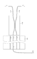
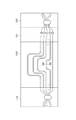
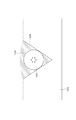
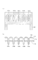
図1A〜図1Fは、本発明の実施例1による回折格子を説明する図である。図1Aは、実施例1の回折格子の構成を示す図である。この回折格子は、第1ブロック101及び第2ブロック102を備える。第1ブロック101は、複数の入力導波路103、スラブ導波路(スターカプラ)104、遅延導波路アレイ105、及び有機材料(例えば樹脂)が充填された細溝106から構成され、第2ブロック102は、複数の入力導波路107、スラブ導波路(スターカプラ)108、及び複数の出力導波路109から構成される。
1A to 1F are diagrams for explaining a diffraction grating according to a first embodiment of the present invention. FIG. 1A is a diagram illustrating the configuration of the diffraction grating according to the first embodiment. The diffraction grating includes a
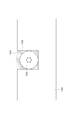
図1Bは、実施例1の回折格子の構成を示す断面図である。第1ブロック101と第2ブロック102は、共通の保持基板110上に貼り付けて接合される。
FIG. 1B is a cross-sectional view illustrating the configuration of the diffraction grating according to the first embodiment. The
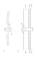
図1Cは、第1ブロック101における「A」の箇所、即ち、細溝106の拡大図である。図1C(a)は上面図、図1C(b)は断面図である。上部クラッド層113、コア層114、及び下部クラッド層115が導波路を形成している。ここで、溝111は下部クラッド層115まで掘られていて、幅5〜30ミクロン程度であり、屈折率調整された樹脂112が充填されている。約10 μm幅(W)の溝を設け、導波路の有効屈折率(n = 1.453)とほぼ等しく屈折率調整した樹脂を充填、硬化させて位相調整を行う。溝幅の誤差(δW)は±0.1μm、樹脂の屈折率誤差(δn)は±0.001程度である。このとき位相補償誤差の範囲は、
±2π×(nδW+δnW)/λo (1)
と近似される。中心波長(λo)を1.55μmと仮定すると、溝幅誤差の影響が主になり、±0.6 radの精度での絶対位相制御、±0.3 radの精度での相対位相制御が可能になる。アレイ導波路回折格子の場合は、相対位相の誤差が問題になるが、この方法を用いて位相調整が可能である。しかしながら、位相調整を行うためには、導波路間の相対的な位相(光路長)の測定が必須である。本発明では、アレイ導波路の途中で回路を切断しているため、相対位相の測定が容易にできる。
FIG. 1C is an enlarged view of the portion “A” in the
± 2π × (nδW + δnW) / λo (1)
Is approximated by Assuming that the center wavelength (λo) is 1.55 μm, the effect of groove width error is the main factor, and absolute phase control with an accuracy of ± 0.6 rad and relative phase control with an accuracy of ± 0.3 rad are possible. In the case of an arrayed waveguide grating, an error in relative phase becomes a problem, but phase adjustment is possible using this method. However, in order to adjust the phase, it is essential to measure the relative phase (optical path length) between the waveguides. In the present invention, since the circuit is cut in the middle of the arrayed waveguide, the relative phase can be easily measured.
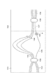
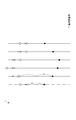
図1Dは、相対位相測定法を説明する図である。第1ブロック101に入射した単一波長の光(CW光)は、各アレイ導波路に分配される。干渉用導波路116は、アレイ導波路からの二つの出力と結合可能なピッチになっている。図中では隣接する導波路となっているが、離れている導波路の出力でも良い。干渉用導波路116中で二つの出力光が干渉し、二つの出力ポート117、118に分岐して出力される。このとき、アレイ導波路の出力光の位相差δに応じて出力ポート117からの出力光強度I1と出力ポート118からの出力光強度I2は変化する。
FIG. 1D is a diagram illustrating a relative phase measurement method. Single wavelength light (CW light) incident on the
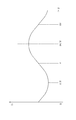
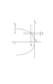
図1Eは、位相差δと出力光強度I1との関係を示す図である。これにより、任意の2本のアレイ導波路間の位相差を測定することが可能となる。順に位相差を測定し、アレイ導波路間の相対位相を測定できる。このようにして、アレイ導波路間の相対位相の測定を行い、相対位相を調整することが可能になる。アレイ導波路回折格子の標準的な設計では、入力導波路107からスラブ導波路108への接続部において中心波長の光を入射した場合の相対位相が0となる。
FIG. 1E is a diagram showing the relationship between the phase difference δ and the output light intensity I1. This makes it possible to measure the phase difference between any two arrayed waveguides. By sequentially measuring the phase difference, the relative phase between the arrayed waveguides can be measured. In this way, the relative phase between the arrayed waveguides can be measured and the relative phase can be adjusted. In the standard design of the arrayed waveguide grating, the relative phase when the light having the center wavelength is incident on the connection portion from the
図1Fは、導波路番号とその導波路の相対位相Φとの関係を示す図である。黒丸印は入力導波路107の相対位相を、三角印は調整前の遅延導波路アレイ105の相対位相を、白丸印は調整後の遅延導波路アレイ105の相対位相を示す。遅延導波路アレイ105の相対位相を前述の方法に従って調整し、白丸印のように設定すれば、遅延導波路アレイ105及び入力導波路107を経てスラブ導波路108に接続する箇所での各導波路間の相対位相を0に近づけること、即ち、光路長誤差(位相誤差)を0に近づけることが可能になる。本構成において、隣接するアレイ導波路間の光路長差ΔLを一定の値に設定することによってアレイ導波路回折格子として動作する。勿論、入力導波路107からスラブ導波路108への接続部において中心波長の光を入射した場合の相対位相を0とせず、任意の設定値に合わせることが可能であることは言うまでもない。この場合は、入力導波路107とスラブ導波路108の接続位置を調整することによってアレイ導波路回折格子として動作する。アレイ導波路回折格子の周波数分解能は、位相誤差補償が行われた場合、遅延線アレイで実現される最大の遅延時間の逆数に比例する。即ち、本実施例では基板寸法制限の許す範囲で、アレイ導波路回折格子の高分解能化を実現することが可能となる。
FIG. 1F is a diagram illustrating a relationship between a waveguide number and a relative phase Φ of the waveguide. Black circles indicate the relative phase of the
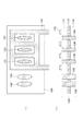
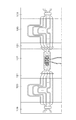
図2A〜図2Cは、本発明の実施例2による回折格子を説明する図である。図2Aは、実施例2の回折格子の構成を示す図である。ここで、第1ブロック119は、複数の入力導波路、スターカプラ、及び複数の出力導波路とから構成される。入射光を複数の導波路に分配する役割を持ち、第2ブロック120は、基板上に設けられた複数の溝構造に、ホーリーファイバを埋め込んで構成される。第3ブロック121は、複数の遅延導波路、及びそれらの導波路に設けられ、有機材料が充填された溝から構成され、位相制御のためのものである。第4ブロック122は、複数の入力導波路、スターカプラ、及び複数の出力導波路とから構成される。
2A to 2C are views for explaining a diffraction grating according to a second embodiment of the present invention. FIG. 2A is a diagram illustrating a configuration of the diffraction grating according to the second embodiment. Here, the
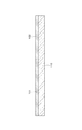
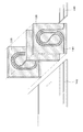
図2B及び図2Cは、第2ブロック120の2B−2B’における、2つの例の場合の断面図を示す。ここで、ホーリーファイバ123は、第2ブロック120におけるホーリーファイバ保持用の溝125、126に固定用樹脂124によって固定されている。溝125、126は、ダイシング、ドライエッチング、ウエットエッチング等で形成する。典型的なコア周囲に6箇所のホールのあるホーリーファイバ123では、曲げ半径2 mmで一巻きの曲げ損失が0.01dB程度である。このため、多数回の曲げを設けても損失の増加は僅かである。また、伝搬損失は0.0005 dB/m以下である。これに対して、比屈折率差1.5%の石英導波路の曲げ損失は同水準であるが、伝搬損失は3 dB/mと大きい。溝作製後に、ファイバをはめ込み、樹脂を充填硬化させて、保持基板の両端を研磨してブロックが作製される。ドライエッチングの場合、溝の位置精度は±0.5μm程度であり、ファイバのコア位置の偏差はさらに小さい。これらの位置ずれから見積もると、ファイバ長手方向の長さを1m、180度の曲げが20回あると仮定すると、長さの誤差は±5μm程度と推定される。しかしながら、アレイ導波路回折格子として重要なことは、隣接する遅延線の長さの差ΔLの設定値からのずれである。ΔLの設定値が2 mmであれば、ずれは±10 nmとなるので無視できるほど少ない。第1ブロック119、第2ブロック120、第3ブロック121を接合後、実施例1と同様にして相対位相の測定と位相調整を行い、さらに、第4ブロック122を接合してアレイ導波路回折格子が完成する。実施例1と比較すると、遅延線の保持基板には均一な薄膜成長など不要なので大面積基板を利用することが可能であり、例えば、シリコン基板では12インチ基板まで商用品が利用可能である。また、光導波路よりもホーリーファイバの伝搬損失は桁違いに小さいので、長尺な遅延線を実現することが可能である。よって、位相補償されるならば、実施例1よりも更に高分解能な回折格子を実現することが可能である。
2B and 2C are cross-sectional views showing two examples of 2B-2B ′ of the
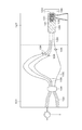
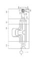
図3A〜図3Dは、本発明の実施例3による分散補償回路を説明する図である。図3Aは、実施例3の分散補償回路の構成を示す図である。第1ブロック101は、実施例1の第1ブロック101と同様である。第2ブロック127は、可変分散補償ブロックであり、入出力導波路128、スラブ導波路129、温度制御しない導波路レンズ130、温度制御する導波路レンズ131、ヒータ132、ミラー133、及びミラー保持基板134を有する。ミラー133は、第1ブロック101と第2ブロック127で構成される回折格子の空間的フリースペクトラルレンジに合わせてある。回折格子の分光面にミラーを配置し、その近傍にレンズを設けて分散補償する光回路は公知である。本実施例の特徴は、実施例1と同様の方法で構成されたアレイ導波路を利用するので、位相誤差を少なくしたり、あるいは、入出力導波路128とスラブ導波路129との接続箇所での位相を制御したりして、分散補償回路の損失を低減したり、あるいは、レンズ設計の自由度を高めることができる点である。また、もう一つの特徴として、温度制御して焦点距離を変化させるレンズと、温度制御せずに焦点距離を変化させないレンズを配置する点である。平面状のミラー133に対して、ある温度で2次分散が特定の値を持つように設計すると、レンズの焦点距離が一意的に決定され、温度制御による位相制御量が十分に得られない場合がある。しかしながら、温度制御せずに焦点距離を変化させないレンズによって分散補償量にバイアスをかけることができるのでこの問題が解決できる。
3A to 3D are diagrams for explaining a dispersion compensation circuit according to a third embodiment of the present invention. FIG. 3A is a diagram illustrating a configuration of the dispersion compensation circuit according to the third embodiment. The
図3Bは、レンズ周辺の拡大図である。図3B(a)は上面図、図3B(b)は断面図である。ここで、樹脂135、136が溝に充填されている。ここでは、レンズ形状は凸型であるが、凹型のレンズ、メニスカス型レンズ、平凸レンズ、平凹レンズも利用可能である。形状だけでなく、樹脂屈折率をスラブ導波路屈折率に比較して大きくするか、小さくするかを選択することによってもレンズの正負を選択することが可能である。また、導波路レンズ130に樹脂を入れず、温度依存性が生じない構造も利用可能である。
FIG. 3B is an enlarged view around the lens. 3B (a) is a top view and FIG. 3B (b) is a cross-sectional view. Here, the
図3Cは、可変分散補償の原理を説明する図である。本実施例3の素子の入出力スペクトル特性において、中心角周波数をωoとすると、フーリエ位相φが次式を満たすとき、
φ=a(ω−ωo)2 (2)
素子は、aに比例する二次分散値を持つ。また、aはスペクトル分光面である反射ミラー近傍に配置されたレンズ群の焦点距離に比例する。さらに、この焦点距離は、レンズを構成する樹脂の屈折率によって変化するので、ヒータ132によって、局所的にレンズ温度を制御し、ひいては、二次分散値を制御することが可能になる。また、aの設定可能な範囲は回折格子部の周波数分解能に比例する。何故ならば、図中のδωを周波数分解能とするとき、この範囲での位相変化δφが十分に小さい(π/16)必要があるからである。本発明では、高分解能回折格子が実現されるので、必然的に分散補償可能量も増大する。
FIG. 3C is a diagram illustrating the principle of variable dispersion compensation. In the input / output spectral characteristics of the element of Example 3, when the center angular frequency is ωo, the Fourier phase φ satisfies the following equation:
φ = a (ω−ωo) 2 (2)
The element has a secondary dispersion value proportional to a. Further, a is proportional to the focal length of the lens group arranged in the vicinity of the reflection mirror that is the spectral spectral plane. Further, since this focal length varies depending on the refractive index of the resin constituting the lens, the lens temperature can be locally controlled by the
図3Dは、他のレンズ構成の例のレンズ周辺の拡大図である。図3D(a)は上面図、図3D(b)は断面図である。ここでは、樹脂136aと樹脂136bは異なる屈折率を有する。レンズ131aには樹脂136aが充填され、レンズ131bには樹脂136bが充填されている。例えば、レンズ131aとレンズ131bのどちらも凸レンズ形状で、樹脂136aの屈折率がスラブ導波路の有効屈折率よりも大きく、樹脂136bの屈折率がスラブ導波路の有効屈折率よりも小さい場合には、レンズ131aは凸レンズの機能を有し、レンズ131bは凹レンズの機能を有する。即ち、あるレンズ系の焦点距離を得るために、両レンズの形状と両樹脂の屈折率を調整することによってレンズ段数を幅広く設定することができる。樹脂の屈折率温度依存性は常に負であるので、トータルの段数を増やすことによって温度変化による位相変化量を増やすことができる。即ち、本構成によっても、分散補償量とレンズ系の焦点距離を独立に設定することが可能である。
FIG. 3D is an enlarged view of the periphery of the lens of another example of the lens configuration. 3D (a) is a top view and FIG. 3D (b) is a cross-sectional view. Here, the
図4は、本発明の実施例4による分散補償回路の構成を説明する図である。本実施例4は、実施例2の第1ブロック119、第2ブロック120、第3ブロック121に実施例3の第2ブロック(可変分散補償ブロック)127を接合したものである。実施例1よりも回折格子の高分解能化が可能であるため、分散補償量も更に大きくできる利点がある。
FIG. 4 is a diagram for explaining the configuration of a dispersion compensation circuit according to the fourth embodiment of the present invention. In the fourth embodiment, the second block (variable dispersion compensation block) 127 of the third embodiment is joined to the
図5は、本発明の実施例5による分散補償回路の構成を説明する図である。本実施例5は、分散補償器を透過型で構成したもので二つの第1ブロック101に、透過型構成の可変分散補償ブロック137を接合している。透過型にすることによって、入出力に光サーキュレータが不要になる。
FIG. 5 is a diagram for explaining the configuration of a dispersion compensation circuit according to the fifth embodiment of the present invention. In the fifth embodiment, a dispersion compensator is configured as a transmission type, and a variable
図6は、本発明の実施例6による分散補償回路の構成を説明する図である。本実施例6は、分散補償器を透過型で構成したもので二つの第1ブロック119、第2ブロック120、第3ブロック121に、透過型構成の可変分散補償ブロック137を接合している。透過型にすることによって、入出力に光サーキュレータが不要になる。
FIG. 6 is a diagram for explaining the configuration of a dispersion compensation circuit according to the sixth embodiment of the present invention. In the sixth embodiment, a dispersion compensator is configured as a transmission type, and a variable
図7は、本発明の実施例7による回折格子及び分散補償回路の構成を説明する図である。本実施例7は、前記実施例2、4、6における第2ブロック120の代わりに、複数の入力導波路142、遅延導波路141を有する基板138が積層されている光遅延線アレイ、及び複数の出力導波路143からなるブロック構成とする。複数の基板を利用するため長尺の遅延導波路を実現可能である。
FIG. 7 is a diagram illustrating the configuration of the diffraction grating and the dispersion compensation circuit according to the seventh embodiment of the present invention. In the seventh embodiment, instead of the
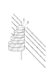
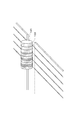
図8A及び図8Bは、本発明の実施例8による回折格子及び分散補償回路の構成を説明する図である。本実施例8は、前記実施例2、4、6における第2ブロック120の代わりに、ボビン139、140にホーリーファイバ123を巻き付けて構成されている光遅延線アレイを有するブロック構成とする。遅延線が長尺である場合に、小型化に有効である。
8A and 8B are diagrams for explaining the configuration of the diffraction grating and the dispersion compensation circuit according to the eighth embodiment of the present invention. In the eighth embodiment, instead of the
なお、本発明は上記実施例に限定されるものではない。
実施例2、4、7、8において、図2、図4に図示する第1〜第4ブロックはこの順に接続されていても良いし、第2ブロックと第3ブロックの順序を逆にして、第1、第3、第2、第4ブロックの順に接続されていても良い。すわなち、第1ブロック及び第4ブロックを両端にして、第1〜第4ブロックが接続されていれば良い。
In addition, this invention is not limited to the said Example.
In Examples 2, 4, 7, and 8, the first to fourth blocks illustrated in FIGS. 2 and 4 may be connected in this order, or the order of the second block and the third block may be reversed. The first, third, second, and fourth blocks may be connected in this order. That is, it is only necessary that the first to fourth blocks are connected with the first block and the fourth block at both ends.
101:第1ブロック、102:第2ブロック、103:複数の入力導波路、
104:スラブ導波路、105:遅延導波路アレイ、106:樹脂充填された細溝、
107:複数の入力導波路、108:スラブ導波路、109:複数の出力導波路、
110:共通の保持基板、111:溝、112:樹脂、113:上部クラッド層、
114:コア層、115:下部クラッド層、116:干渉用導波路、
117:出力ポート、118:出力ポート、119:第1ブロック、
120:第2ブロック、121:第3ブロック、122:第4ブロック、
123:ホーリーファイバ、124:固定用樹脂、
125、126:ホーリーファイバ保持用溝、127:可変分散補償ブロック、
128:入出力導波路、129:スラブ導波路、130:温度制御しない導波路レンズ、
131:温度制御する導波路レンズ、132:ヒータ、133:ミラー、
134:ミラー保持基板、135、136:樹脂、
137:透過型構成の可変分散補償ブロック、138:遅延導波路を有する基板、
139、140:ボビン、142:入力導波路、143:出力導波路
101: first block, 102: second block, 103: a plurality of input waveguides,
104: Slab waveguide, 105: Delayed waveguide array, 106: Fine groove filled with resin,
107: a plurality of input waveguides, 108: a slab waveguide, 109: a plurality of output waveguides,
110: Common holding substrate, 111: Groove, 112: Resin, 113: Upper clad layer,
114: Core layer, 115: Lower cladding layer, 116: Interference waveguide,
117: output port, 118: output port, 119: first block,
120: 2nd block, 121: 3rd block, 122: 4th block,
123: holey fiber, 124: resin for fixing,
125, 126: grooves for holding a holey fiber, 127: a variable dispersion compensation block,
128: input / output waveguide, 129: slab waveguide, 130: waveguide lens without temperature control,
131: Waveguide lens for temperature control, 132: Heater, 133: Mirror,
134: Mirror holding substrate, 135, 136: Resin,
137: Variable dispersion compensation block of transmission type configuration, 138: Substrate having delay waveguide,
139, 140: bobbin, 142: input waveguide, 143: output waveguide
Claims (7)
複数の第1入力導波路と、
該第1入力導波路に接続されている第1スターカプラと、
該第1スターカプラに接続されている複数の第1出力導波路と
を有する第1ブロックと、
(b)
基板上に設けられている複数の溝構造に、遅延線を構成し互いに光路長の異なるホーリーファイバを埋め込んで構成されている第2ブロックと、
(c)
複数の遅延導波路と、
該複数の遅延導波路の各々の一部に代えて設けられ、位相測定用光回路と接続されて該複数の遅延導波路間の相対位相が測定され、該相対位相の位相誤差を補償する屈折率調整した有機材料が充填されている複数の溝と
を有する第3ブロックと、
(d)
複数の第2入力導波路と、
該第2入力導波路に接続されている第2スターカプラと、
該第2スターカプラに接続されている複数の第2出力導波路と
を有する第4ブロックと
を備え、第1ブロック及び第4ブロックを両端にして、第1〜第4ブロックが接続されていることを特徴とする回折格子。 (a)
A plurality of first input waveguides;
A first star coupler connected to the first input waveguide;
A first block having a plurality of first output waveguides connected to the first star coupler;
(b)
A plurality of groove structure provided on the substrate, and a second block configured by embedding different Do that holey fiber structure and the optical path lengths from each other delay lines,
(c)
A plurality of delay waveguides;
Refraction that is provided in place of a part of each of the plurality of delay waveguides, is connected to a phase measuring optical circuit, measures the relative phase between the plurality of delay waveguides, and compensates for the phase error of the relative phase A third block having a plurality of grooves filled with a rate-adjusted organic material;
(d)
A plurality of second input waveguides;
A second star coupler connected to the second input waveguide;
And a fourth block having a plurality of second output waveguides connected to the second star coupler, and the first to fourth blocks are connected with the first block and the fourth block at both ends. A diffraction grating characterized by that.
複数の第1入力導波路と、
該第1入力導波路に接続されているスターカプラと、
該スターカプラに接続されていて互いに光路長の異なる複数の遅延導波路と、
該複数の遅延導波路の各々の一部に代えて設けられ、位相測定用光回路と接続されて該複数の遅延導波路間の相対位相が測定され、該相対位相の位相誤差を補償する屈折率調整した有機材料が充填されている複数の第1溝と
を有する第1ブロックと、
(b)
複数の第2入力導波路と、
該第2入力導波路に接続されているスラブ導波路と、
該スラブ導波路の光路上に設けられ、有機材料が充填されて導波路レンズを構成する複数の第2溝と、
該複数の第2溝の内の一部の第2溝の周囲に設けられ、該複数の第2溝の内の一部の第2溝のみの温度を制御するヒータと、
前記スラブ導波路端であり基板の端面に設けられているミラーと
を有し、前記第1ブロックに接続されている第2ブロックと
を備えることを特徴とする分散補償回路。 (a)
A plurality of first input waveguides;
A star coupler connected to the first input waveguide;
A plurality of delay waveguides that Do different optical path lengths from each other have been connected to the star coupler,
Refraction that is provided in place of a part of each of the plurality of delay waveguides, is connected to a phase measuring optical circuit, measures the relative phase between the plurality of delay waveguides, and compensates for the phase error of the relative phase A first block having a plurality of first grooves filled with a rate-adjusted organic material;
(b)
A plurality of second input waveguides;
A slab waveguide connected to the second input waveguide;
A plurality of second grooves provided on the optical path of the slab waveguide and filled with an organic material to form a waveguide lens;
A heater that is provided around a part of the second grooves in the plurality of second grooves and controls the temperature of only a part of the second grooves in the plurality of second grooves ;
A dispersion compensation circuit comprising: a second block connected to the first block and having a mirror provided at an end surface of the substrate that is an end of the slab waveguide.
複数の第1入力導波路と、
該第1入力導波路に接続されている第1スターカプラと、
該第1スターカプラに接続されている複数の出力導波路と
を有する第1ブロックと、
(b)
基板上に設けられている複数の溝構造に、遅延線を構成し互いに光路長の異なるホーリーファイバを埋め込んで構成されている第2ブロックと、
(c)
複数の遅延導波路と、
該複数の遅延導波路の各々の一部に代えて設けられ、位相測定用光回路と接続されて該複数の遅延導波路間の相対位相が測定され、該相対位相の位相誤差を補償する屈折率調整した有機材料が充填されている複数の溝と
を有する第3ブロックと、
(d)
複数の第2入力導波路と、
該第2入力導波路に接続されているスラブ導波路と、
該スラブ導波路の光路上に設けられ、有機材料が充填されて導波路レンズを構成する溝と、
該溝周囲に設けられているヒータと、
前記スラブ導波路端であり基板の端面に設けられているミラーと
を有する第4ブロックと
を備え、第1ブロック及び第4ブロックを両端にして、第1〜第4ブロックが接続されていることを特徴とする分散補償回路。 (a)
A plurality of first input waveguides;
A first star coupler connected to the first input waveguide;
A first block having a plurality of output waveguides connected to the first star coupler;
(b)
A plurality of groove structure provided on the substrate, and a second block configured by embedding different Do that holey fiber structure and the optical path lengths from each other delay lines,
(c)
A plurality of delay waveguides;
Refraction that is provided in place of a part of each of the plurality of delay waveguides, is connected to a phase measuring optical circuit, measures the relative phase between the plurality of delay waveguides, and compensates for the phase error of the relative phase A third block having a plurality of grooves filled with a rate-adjusted organic material;
(d)
A plurality of second input waveguides;
A slab waveguide connected to the second input waveguide;
A groove provided on the optical path of the slab waveguide and filled with an organic material to form a waveguide lens;
A heater provided around the groove;
A fourth block having a mirror provided at an end surface of the substrate, which is an end of the slab waveguide, and the first to fourth blocks are connected to each other with the first block and the fourth block at both ends. A dispersion compensation circuit characterized by the above.
複数の第1入力導波路と、
該第1入力導波路に接続されている第1スターカプラと、
該第1スターカプラに接続されていて互いに光路長の異なる複数の第1遅延導波路と、
該複数の第1遅延導波路の各々の一部に代えて設けられ、位相測定用光回路と接続されて該複数の第1遅延導波路間の相対位相が測定され、該相対位相の位相誤差を補償する屈折率調整した有機材料が充填されている複数の第1溝と
を有する第1ブロックと、
(b)
複数の第2入力導波路と、
該第2入力導波路に接続されているスラブ導波路と、
該スラブ導波路の光路上に設けられ、有機材料が充填されて導波路レンズを構成する複数の第2溝と、
該複数の第2溝の内の一部の第2溝の周囲に設けられ、該複数の第2溝の内の一部の第2溝のみの温度を制御するヒータと、
前記スラブ導波路に接続されている複数の第2出力導波路と
を有する第2ブロックと、
(c)
複数の第2遅延導波路と、
互いに光路長の異なる該複数の第2遅延導波路の各々の一部に代えて設けられ、位相測定用光回路と接続されて該複数の第2遅延導波路間の相対位相が測定され、該相対位相の位相誤差を補償する屈折率調整した有機材料が充填されている複数の第3溝と、
前記第2遅延導波路に接続されている第2スターカプラと、
該第2スターカプラに接続されている複数の第3出力導波路と
を有する第3ブロックと
を備え、第1〜第3ブロックがこの順に接続されていることを特徴とする分散補償回路。 (a)
A plurality of first input waveguides;
A first star coupler connected to the first input waveguide;
A plurality of first delay waveguide that Do different optical path lengths from each other be connected to the first star coupler,
Instead of each of the plurality of first delay waveguides, the relative phase between the plurality of first delay waveguides is measured by connecting to a phase measuring optical circuit, and a phase error of the relative phase is measured. A first block having a plurality of first grooves filled with an organic material having a refractive index adjusted to compensate for
(b)
A plurality of second input waveguides;
A slab waveguide connected to the second input waveguide;
A plurality of second grooves provided on the optical path of the slab waveguide and filled with an organic material to form a waveguide lens;
A heater that is provided around a part of the second grooves in the plurality of second grooves and controls the temperature of only a part of the second grooves in the plurality of second grooves ;
A second block having a plurality of second output waveguides connected to the slab waveguide;
(c)
A plurality of second delay waveguides;
Provided in place of a part of each of the plurality of second delay waveguides having different optical path lengths, connected to a phase measuring optical circuit, and measuring a relative phase between the plurality of second delay waveguides; A plurality of third grooves filled with an organic material whose refractive index is adjusted to compensate for a phase error of the relative phase;
A second star coupler connected to the second delay waveguide;
A dispersion compensation circuit comprising: a third block having a plurality of third output waveguides connected to the second star coupler, wherein the first to third blocks are connected in this order.
複数の第1入力導波路と、
該第1入力導波路に接続されている第1スターカプラと、
該第1スターカプラに接続されている複数の第1出力導波路と
を有する第1ブロックと、
(b)
基板上に設けられている複数の第1溝構造に、遅延線を構成し互いに光路長の異なる第1ホーリーファイバを埋め込んで構成されている第2ブロックと、
(c)
複数の第1遅延導波路と、
該複数の第1遅延導波路の各々の一部に代えて設けられ、位相測定用光回路と接続されて該複数の第1遅延導波路間の相対位相が測定され、該相対位相の位相誤差を補償する屈折率調整した有機材料が充填されている複数の第1溝と
を有する第3ブロックと、
(d)
複数の第2入力導波路と、
該第2入力導波路に接続されているスラブ導波路と、
該スラブ導波路の光路上に設けられ、有機材料が充填されて導波路レンズを構成する第2溝と、
該第2溝周囲に設けられているヒータと、
前記スラブ導波路に接続されている複数の第2出力導波路と
を有する第4ブロックと、
(e)
複数の第2遅延導波路と、
該複数の第2遅延導波路の各々の一部に代えて設けられ、位相測定用光回路と接続されて該複数の第2遅延導波路間の相対位相が測定され、該相対位相の位相誤差を補償する屈折率調整した有機材料が充填されている複数の第3溝と
を有する第5ブロックと、
(f)
基板上に設けられている複数の第2溝構造に、遅延線を構成し互いに光路長の異なる第2ホーリーファイバを埋め込んで構成されている第6ブロックと、
(g)
複数の第3入力導波路と、
該第3入力導波路に接続されている第2スターカプラと、
該第2スターカプラに接続されている複数の第3出力導波路と
を有する第7ブロックと
を備え、第1〜第7ブロックがこの順に接続されていることを特徴とする分散補償回路。 (a)
A plurality of first input waveguides;
A first star coupler connected to the first input waveguide;
A first block having a plurality of first output waveguides connected to the first star coupler;
(b)
A plurality of first groove structure provided on the substrate, and a second block configured by embedding the first holey fiber that different Do configuration and optical path lengths from each other delay lines,
(c)
A plurality of first delay waveguides;
Instead of each of the plurality of first delay waveguides, the relative phase between the plurality of first delay waveguides is measured by connecting to a phase measuring optical circuit, and a phase error of the relative phase is measured. A third block having a plurality of first grooves filled with an organic material having a refractive index adjusted to compensate for
(d)
A plurality of second input waveguides;
A slab waveguide connected to the second input waveguide;
A second groove provided on the optical path of the slab waveguide and filled with an organic material to form a waveguide lens;
A heater provided around the second groove;
A fourth block having a plurality of second output waveguides connected to the slab waveguide;
(e)
A plurality of second delay waveguides;
Instead of each of the plurality of second delay waveguides, the relative phase between the plurality of second delay waveguides is measured by connecting to a phase measuring optical circuit, and a phase error of the relative phase is measured. A fifth block having a plurality of third grooves filled with an organic material having a refractive index adjusted to compensate for
(f)
A plurality of second groove structure provided on a substrate, a sixth block is configured by embedding the second holey fiber that different Do configuration and optical path lengths from each other delay lines,
(g)
A plurality of third input waveguides;
A second star coupler connected to the third input waveguide;
And a seventh block having a plurality of third output waveguides connected to the second star coupler, wherein the first to seventh blocks are connected in this order.
複数の第1入力導波路と、
該第1入力導波路に接続されている第1スターカプラと、
該第1スターカプラに接続されている複数の第1出力導波路と
を有する第1ブロックと、
(b)
複数の第2入力導波路を有する入力導波路基板と、
該入力導波路基板の複数の各第2入力導波路に接続されていて互いに光路長の異なる遅延導波路又は互いに光路長の異なるホーリーファイバ埋め込みの遅延線を有する複数積層された基板と、
該基板の遅延導波路又は遅延線に接続されている複数の第2出力導波路を有する出力導波路基板と
を有する第2ブロックと、
(c)
複数の遅延導波路と、
該複数の遅延導波路の各々の一部に代えて設けられ、位相測定用光回路と接続されて該複数の遅延導波路間の相対位相が測定され、該相対位相の位相誤差を補償する屈折率調整した有機材料が充填されている複数の溝と
を有する第3ブロックと、
(d)
複数の第3入力導波路と、
該第3入力導波路に接続されている第2スターカプラと、
該第2スターカプラに接続されている複数の第3出力導波路と
を有する第4ブロックと
を備え、第1ブロック及び第4ブロックを両端にして、第1〜第4ブロックが接続されていることを特徴とする回折格子。 (a)
A plurality of first input waveguides;
A first star coupler connected to the first input waveguide;
A first block having a plurality of first output waveguides connected to the first star coupler;
(b)
An input waveguide substrate having a plurality of second input waveguides;
A substrate formed by stacking a plurality having embedded delay line different Do that delay waveguide or different holey fiber optical path lengths from each other in optical path length to each other more are connected to the respective second input waveguides of the input waveguide substrate,
A second block having an output waveguide substrate having a plurality of second output waveguides connected to the delay waveguide or delay line of the substrate;
(c)
A plurality of delay waveguides;
Refraction that is provided in place of a part of each of the plurality of delay waveguides, is connected to a phase measuring optical circuit, measures the relative phase between the plurality of delay waveguides, and compensates for the phase error of the relative phase A third block having a plurality of grooves filled with a rate-adjusted organic material;
(d)
A plurality of third input waveguides;
A second star coupler connected to the third input waveguide;
And a fourth block having a plurality of third output waveguides connected to the second star coupler, and the first to fourth blocks are connected with the first block and the fourth block at both ends. A diffraction grating characterized by that.
複数の第1入力導波路と、
該第1入力導波路に接続されている第1スターカプラと、
該第1スターカプラに接続されている複数の第1出力導波路と
を有する第1ブロックと、
(b)
複数の第2入力導波路を有する入力導波路基板と、
該入力導波路基板の複数の各第2入力導波路に接続されている遅延線を構成し互いに光路長の異なるホーリーファイバを巻き付けた円柱状ボビンと、
該ホーリーファイバに接続されている複数の第2出力導波路を有する出力導波路基板と
を有する第2ブロックと、
(c)
複数の遅延導波路と、
該複数の遅延導波路の各々の一部に代えて設けられ、位相測定用光回路と接続されて該複数の遅延導波路間の相対位相が測定され、該相対位相の位相誤差を補償する屈折率調整した有機材料が充填されている複数の溝と
を有する第3ブロックと、
(d)
複数の第3入力導波路と、
該第3入力導波路に接続されている第2スターカプラと、
該第2スターカプラに接続されている複数の第3出力導波路と
を有する第4ブロックと
を備え、第1ブロック及び第4ブロックを両端にして、第1〜第4ブロックが接続されていることを特徴とする回折格子。 (a)
A plurality of first input waveguides;
A first star coupler connected to the first input waveguide;
A first block having a plurality of first output waveguides connected to the first star coupler;
(b)
An input waveguide substrate having a plurality of second input waveguides;
A cylindrical bobbin winding the input waveguide several different that holey fiber of each of the second input waveguide the attached constitute a delay line optical path lengths from each other of the substrate,
A second block having an output waveguide substrate having a plurality of second output waveguides connected to the holey fiber;
(c)
A plurality of delay waveguides;
Refraction that is provided in place of a part of each of the plurality of delay waveguides, is connected to a phase measuring optical circuit, measures the relative phase between the plurality of delay waveguides, and compensates for the phase error of the relative phase A third block having a plurality of grooves filled with a rate-adjusted organic material;
(d)
A plurality of third input waveguides;
A second star coupler connected to the third input waveguide;
And a fourth block having a plurality of third output waveguides connected to the second star coupler, and the first to fourth blocks are connected with the first block and the fourth block at both ends. A diffraction grating characterized by that.
Priority Applications (2)
| Application Number | Priority Date | Filing Date | Title |
|---|---|---|---|
| JP2006213547A JP4385168B2 (en) | 2006-08-04 | 2006-08-04 | Diffraction grating and dispersion compensation circuit |
| US11/882,511 US7496256B2 (en) | 2006-08-04 | 2007-08-02 | Diffraction grating and dispersion compensation circuit |
Applications Claiming Priority (1)
| Application Number | Priority Date | Filing Date | Title |
|---|---|---|---|
| JP2006213547A JP4385168B2 (en) | 2006-08-04 | 2006-08-04 | Diffraction grating and dispersion compensation circuit |
Publications (2)
| Publication Number | Publication Date |
|---|---|
| JP2008040094A JP2008040094A (en) | 2008-02-21 |
| JP4385168B2 true JP4385168B2 (en) | 2009-12-16 |
Family
ID=39151643
Family Applications (1)
| Application Number | Title | Priority Date | Filing Date |
|---|---|---|---|
| JP2006213547A Active JP4385168B2 (en) | 2006-08-04 | 2006-08-04 | Diffraction grating and dispersion compensation circuit |
Country Status (2)
| Country | Link |
|---|---|
| US (1) | US7496256B2 (en) |
| JP (1) | JP4385168B2 (en) |
Families Citing this family (10)
| Publication number | Priority date | Publication date | Assignee | Title |
|---|---|---|---|---|
| KR100841223B1 (en) * | 2006-02-28 | 2008-06-26 | (주)포인테크 | Temperature-Independent Optical Waveguide Grating Circuit Device for Compensation of Optical Characteristics and Fabrication Method thereof |
| US8340484B2 (en) * | 2010-01-05 | 2012-12-25 | Board Of Regents, The University Of Texas System | Compact multi-port optical signal processor |
| JP5432072B2 (en) * | 2010-06-25 | 2014-03-05 | 日本電信電話株式会社 | Waveguide type optical dispersion compensator |
| US8824056B2 (en) | 2011-03-28 | 2014-09-02 | Gemfire Corporation | Optical device with reduced polarization sensitivity |
| ES2540378B1 (en) * | 2013-12-05 | 2016-05-18 | Univ Politècnica De València | INTEGRATED PHOTONIC DEVICE |
| JP2015215578A (en) * | 2014-05-13 | 2015-12-03 | 日本電信電話株式会社 | Optical waveguide device and polarization separator using the same |
| JP2015219317A (en) * | 2014-05-15 | 2015-12-07 | 日本電信電話株式会社 | Polarization separation circuit |
| JP6219887B2 (en) * | 2015-06-25 | 2017-10-25 | Nttエレクトロニクス株式会社 | Optical waveguide device |
| WO2025248796A1 (en) * | 2024-05-31 | 2025-12-04 | 三菱電機株式会社 | Wavelength dispersion compensation device, optical distance measurement device, and wavelength dispersion compensation method |
| JP7693147B1 (en) * | 2024-05-31 | 2025-06-16 | 三菱電機株式会社 | Wavelength dispersion compensation device, optical distance measuring device, and wavelength dispersion compensation method |
Family Cites Families (17)
| Publication number | Priority date | Publication date | Assignee | Title |
|---|---|---|---|---|
| JP3501235B2 (en) * | 1993-05-07 | 2004-03-02 | 日本電信電話株式会社 | Waveguide type optical device |
| EP0639782B1 (en) * | 1993-08-02 | 1999-11-10 | Nippon Telegraph And Telephone Corporation | Integrated optical waveguide circuit and optical branch line test system using the same |
| JPH10186151A (en) | 1996-12-20 | 1998-07-14 | Nippon Telegr & Teleph Corp <Ntt> | Optical waveguide device and phase adjustment method for optical waveguide device |
| FR2770307B1 (en) * | 1997-10-27 | 1999-11-26 | Commissariat Energie Atomique | PHASE ARRAY OR PHASAR DEVICE AND MANUFACTURING METHOD THEREOF |
| JPH11287916A (en) | 1998-04-01 | 1999-10-19 | Nippon Telegr & Teleph Corp <Ntt> | Optical waveguide device |
| JP2000206348A (en) * | 1999-01-13 | 2000-07-28 | Furukawa Electric Co Ltd:The | Compensation method of light transmission wavelength of optical waveguide circuit |
| JP2000241637A (en) | 1999-02-19 | 2000-09-08 | Sumitomo Electric Ind Ltd | Manufacturing method of optical wavelength multiplexer / demultiplexer |
| US6546161B2 (en) * | 2000-01-21 | 2003-04-08 | Nippon Telegraph And Telephone Corporation | No polarization dependent waveguide type optical circuit |
| US6466707B1 (en) * | 2000-08-21 | 2002-10-15 | Corning Incorporated | Phasar athermalization using a slab waveguide |
| JP3630085B2 (en) * | 2000-09-14 | 2005-03-16 | 日本電気株式会社 | Method for manufacturing arrayed waveguide grating element and arrayed waveguide grating element |
| US20020131683A1 (en) * | 2001-03-15 | 2002-09-19 | Doerr Christopher Richard | Planar lightwave wavelength blocker devices using micromachines |
| US6738545B1 (en) * | 2002-03-18 | 2004-05-18 | Lightwave Microsystems Corporation | Athermal AWG and AWG with low power consumption using groove of changeable width |
| JP3848597B2 (en) | 2002-06-14 | 2006-11-22 | 正隆 中沢 | Manufacturing method of plastic holey fiber |
| WO2004102266A1 (en) * | 2003-05-15 | 2004-11-25 | Fujitsu Limited | Optical switch device |
| US7013065B2 (en) * | 2003-10-22 | 2006-03-14 | Klaus Petermann | Planar optical apparatus for setting the chromatic dispersion in an optical system |
| JP3721565B2 (en) | 2004-02-27 | 2005-11-30 | 学校法人慶應義塾 | Optical functional waveguide, optical modulator, arrayed waveguide diffraction grating, and dispersion compensation circuit |
| JP3866725B2 (en) | 2004-03-03 | 2007-01-10 | 正隆 中沢 | Manufacturing method of plastic holey fiber |
-
2006
- 2006-08-04 JP JP2006213547A patent/JP4385168B2/en active Active
-
2007
- 2007-08-02 US US11/882,511 patent/US7496256B2/en not_active Expired - Fee Related
Also Published As
| Publication number | Publication date |
|---|---|
| US7496256B2 (en) | 2009-02-24 |
| US20080056643A1 (en) | 2008-03-06 |
| JP2008040094A (en) | 2008-02-21 |
Similar Documents
| Publication | Publication Date | Title |
|---|---|---|
| US7496256B2 (en) | Diffraction grating and dispersion compensation circuit | |
| US6501875B2 (en) | Mach-Zehnder inteferometers and applications based on evanescent coupling through side-polished fiber coupling ports | |
| US9069194B2 (en) | Polarization control device | |
| WO2005024469A2 (en) | Interfacing multiple wavelength sources to thin optical waveguides utilizing evanescent coupling | |
| WO2001059495A1 (en) | Waveguide optical interferometer | |
| US11333828B2 (en) | Optical connection component | |
| US20060266743A1 (en) | Laser-ablated fiber devices and method of manufacturing the same | |
| JP6706859B2 (en) | Optical module | |
| US10101535B2 (en) | Single-mode polymer waveguide connector | |
| WO2016056659A1 (en) | Optical component | |
| US7756376B2 (en) | Optical functional waveguide, optical modulator, arrayed waveguide grating, and dispersion compensation circuit | |
| US20120020622A1 (en) | Planar nanophotonic waveguide comprising a structure for optical coupling with an optical fibre | |
| US7335875B2 (en) | Optical branching unit, and method of manufacturing the same | |
| US20210405292A1 (en) | Optical Interconnect Structure and Method for Manufacturing Same | |
| US6819859B2 (en) | Planar lightwave circuit type variable optical attenuator | |
| US7228026B2 (en) | Optical multiplexer/demultiplexer and manufacturing method thereof | |
| JP7464053B2 (en) | Method for aligning optical waveguide element | |
| US20020028040A1 (en) | All-fiber add/drop filter and method of manufacturing the same | |
| JP7348550B2 (en) | optical circuit module | |
| JP3236108U (en) | Optical function integrated device | |
| JP3941613B2 (en) | Optical waveguide circuit and optical waveguide circuit module | |
| JP7244788B2 (en) | Optical fiber connection structure | |
| JP6871106B2 (en) | Optical waveguide chip connection structure | |
| WO2026014298A1 (en) | Optical coupling element | |
| JP6473391B2 (en) | Polarization control element and manufacturing method thereof |
Legal Events
| Date | Code | Title | Description |
|---|---|---|---|
| A131 | Notification of reasons for refusal |
Free format text: JAPANESE INTERMEDIATE CODE: A131 Effective date: 20080430 |
|
| A521 | Written amendment |
Free format text: JAPANESE INTERMEDIATE CODE: A523 Effective date: 20080625 |
|
| A131 | Notification of reasons for refusal |
Free format text: JAPANESE INTERMEDIATE CODE: A131 Effective date: 20090513 |
|
| A521 | Written amendment |
Free format text: JAPANESE INTERMEDIATE CODE: A523 Effective date: 20090701 |
|
| TRDD | Decision of grant or rejection written | ||
| A01 | Written decision to grant a patent or to grant a registration (utility model) |
Free format text: JAPANESE INTERMEDIATE CODE: A01 Effective date: 20090819 |
|
| A01 | Written decision to grant a patent or to grant a registration (utility model) |
Free format text: JAPANESE INTERMEDIATE CODE: A01 |
|
| A61 | First payment of annual fees (during grant procedure) |
Free format text: JAPANESE INTERMEDIATE CODE: A61 Effective date: 20090909 |
|
| R150 | Certificate of patent or registration of utility model |
Free format text: JAPANESE INTERMEDIATE CODE: R150 |
|
| FPAY | Renewal fee payment (event date is renewal date of database) |
Free format text: PAYMENT UNTIL: 20121009 Year of fee payment: 3 |