JP4381970B2 - Developer regulating member, method for producing developer regulating member, developing machine using the same, and image forming apparatus or printer using the developing machine - Google Patents
Developer regulating member, method for producing developer regulating member, developing machine using the same, and image forming apparatus or printer using the developing machine Download PDFInfo
- Publication number
- JP4381970B2 JP4381970B2 JP2004376741A JP2004376741A JP4381970B2 JP 4381970 B2 JP4381970 B2 JP 4381970B2 JP 2004376741 A JP2004376741 A JP 2004376741A JP 2004376741 A JP2004376741 A JP 2004376741A JP 4381970 B2 JP4381970 B2 JP 4381970B2
- Authority
- JP
- Japan
- Prior art keywords
- magnetic plate
- fitting
- plate
- regulating member
- developer regulating
- Prior art date
- Legal status (The legal status is an assumption and is not a legal conclusion. Google has not performed a legal analysis and makes no representation as to the accuracy of the status listed.)
- Expired - Fee Related
Links
Images


Classifications
-
- G—PHYSICS
- G03—PHOTOGRAPHY; CINEMATOGRAPHY; ANALOGOUS TECHNIQUES USING WAVES OTHER THAN OPTICAL WAVES; ELECTROGRAPHY; HOLOGRAPHY
- G03G—ELECTROGRAPHY; ELECTROPHOTOGRAPHY; MAGNETOGRAPHY
- G03G15/00—Apparatus for electrographic processes using a charge pattern
- G03G15/06—Apparatus for electrographic processes using a charge pattern for developing
- G03G15/08—Apparatus for electrographic processes using a charge pattern for developing using a solid developer, e.g. powder developer
- G03G15/0806—Apparatus for electrographic processes using a charge pattern for developing using a solid developer, e.g. powder developer on a donor element, e.g. belt, roller
- G03G15/0812—Apparatus for electrographic processes using a charge pattern for developing using a solid developer, e.g. powder developer on a donor element, e.g. belt, roller characterised by the developer regulating means, e.g. structure of doctor blade
-
- G—PHYSICS
- G03—PHOTOGRAPHY; CINEMATOGRAPHY; ANALOGOUS TECHNIQUES USING WAVES OTHER THAN OPTICAL WAVES; ELECTROGRAPHY; HOLOGRAPHY
- G03G—ELECTROGRAPHY; ELECTROPHOTOGRAPHY; MAGNETOGRAPHY
- G03G2215/00—Apparatus for electrophotographic processes
- G03G2215/01—Apparatus for electrophotographic processes for producing multicoloured copies
- G03G2215/0167—Apparatus for electrophotographic processes for producing multicoloured copies single electrographic recording member
- G03G2215/0174—Apparatus for electrophotographic processes for producing multicoloured copies single electrographic recording member plural rotations of recording member to produce multicoloured copy
- G03G2215/0177—Rotating set of developing units
Landscapes
- Physics & Mathematics (AREA)
- General Physics & Mathematics (AREA)
- Magnetic Brush Developing In Electrophotography (AREA)
- Dry Development In Electrophotography (AREA)
Description
本発明は、マグネットローラの磁力によりトナーを吸引しつつ潜像担持体に向けて供給する現像ローラに臨まされて潜像担持体に供給するトナー量を規制する現像剤規制部材の改良に関し、更にはこの現像剤規制部材の製造方法及びこれを用いた現像機及びこの現像機を用いた複写機、ファクシミリ等の画像形成装置又はプリンタに関する。 The present invention relates to an improvement of a developer regulating member that faces a developing roller that feeds a latent image carrier while attracting toner by the magnetic force of a magnet roller and regulates the amount of toner that is fed to the latent image carrier. Relates to a method for producing the developer regulating member, a developing machine using the developer regulating member, a copying machine using the developing machine, an image forming apparatus such as a facsimile, or a printer .
従来から、画像形成装置又はプリンタには、マグネットローラの磁力により磁性キャリア、トナーを吸着して潜像担持体に向けて供給する現像ローラと、この現像ローラに臨まされて潜像担持体に供給するトナー量を規制する現像剤規制部材(現像ドクター)とを有する現像機が設けられているものが知られている(例えば、特許文献1参照。)。 2. Description of the Related Art Conventionally, an image forming apparatus or printer has a developing roller that attracts a magnetic carrier and toner by a magnetic force of a magnet roller and supplies the toner to a latent image carrier, and is supplied to the latent image carrier by the developing roller. A developing machine having a developer regulating member (developing doctor) that regulates the amount of toner to be performed is known (for example, see Patent Document 1).
この種の現像機は、例えばカラー複写機に用いられ、図1、図2に示すように、現像ローラ1と現像剤規制部材2とを有し、これらは図示を略す現像ケーシング内に設けられている。
This type of developing machine is used for a color copying machine, for example, and has a developing
その現像ローラ1はその現像スリーブ3とマグネットローラ4とを有する。その現像スリーブ3とマグネットローラ4とは駆動軸5によって一体回転される。
The developing
その現像剤規制部材2は、規制板としての非磁性板6と保持板としての磁性板7とから大略構成され、非磁性板6には磁性板7が取り付けられ、マグネットローラ4と磁性板7との間に生じる一様磁界により磁性キャリア、トナーからなる現像剤9が吸引されつつ潜像担持体としての感光体ドラム11に向けて供給される。
The
非磁性板6は、その稜線10が現像スリーブ3の外周に臨まされ、スリーブ3と稜線10との間にギャップGが形成され、非磁性板6の稜線10は画質の安定化を図るためにその吸引された現像剤9の供給量を規制する役割を果たす。
The
なお、その現像剤規制部材2としては、保持板と規制板とを金属板から構成し、規制板の保持板への組み付け方法として、例えば、保持板を半抜き加工してその保持板に嵌合突起を形成し、一方その規制板に嵌合穴を形成し、規制板を保持板に位置決めした後、規制板を保持板に位置決めして挟持する構成のものが知られている(例えば、特許文献2参照)。
ところで、その現像剤規制部材2によるトナー9の供給量の一様化を図るには、ギャップGがその現像ローラの長手方向に一定であることが必要であり、従って、非磁性板6の稜線10の真直度が要求される。ここでは、真直度とは非磁性板6の稜線10の長手方向への直線性をいい、図3に示すように非磁性板6の稜線10を含む面S1に含まれかつ稜線10の延びる方向と直交する方向の直線L1が稜線10と交わる点P1の基準点Oに対する凹凸量ΔLを用いて評価する。
By the way, in order to make the supply amount of the toner 9 uniform by the
その特許文献2に開示のものでは、その現像剤規制部材2による現像剤9の供給量の一様化を図ることができるが、規制板を保持板に組み付けるに際して、ネジ締結作業を行わなければならないために、組み立て作業効率が芳しくないという不都合がある。その保持板を非磁性板6により構成し、その規制板を非磁性板7により構成した場合も同様の不都合がある。
In the one disclosed in
その磁性板7の非磁性板6への組み付け作業には、この他、スポット溶接、YAGレーザ溶接、接着等の各種の手段が知られているが、スポット溶接手段による組み付けでは、溶接歪みが発生するため、真直度の確保が困難であるという問題があり、高画質化が要求されている画像形成装置への対応が困難である。
Various other methods such as spot welding, YAG laser welding, and adhesion are known for assembling the
YAGレーザ溶接手段による組み付けでは、溶接歪みが少ないので高画質化が要求されている画像形成装置への対応は容易であるが、設備コストが高いという面で難点がある。
また、非磁性板7の長手方向に間隔を開けて複数個溶接ポイントを設定して溶接を行わなければならないために、溶接作業効率が芳しくないという不都合もある。
Assembling with the YAG laser welding means is easy to cope with an image forming apparatus that requires high image quality because welding distortion is small, but there is a problem in that the equipment cost is high.
Moreover, since it is necessary to perform welding by setting a plurality of welding points at intervals in the longitudinal direction of the
接着手段による組み付けでは、接着剤の管理、接着治具の製作、接着時間の管理等の各種の管理を行わなければならず、耐久性の観点、経時的観点からは必ずしも芳しくないという不都合がある。 Assembling with an adhesive means requires various managements such as management of adhesives, production of bonding jigs, management of bonding time, and the like, which is not necessarily good from the viewpoint of durability and time. .
本発明は、上記の事情に鑑みて為されたもので、非磁性板に半抜き加工により嵌合突起を形成して、この嵌合突起を用いて磁性板を非磁性板に組み付ける場合でも、生産効率を高めることができ、ひいては非磁性板の真直度の維持に積極的に貢献することのできる現像剤規制部材、この現像剤規制部材の製造方法及びこれを用いた現像機及びこの現像機を用いた画像形成装置又はプリンタを提供することを目的とする。 The present invention has been made in view of the above circumstances, even when a non-magnetic plate is formed with a fitting projection by half-punching, and the magnetic plate is assembled to the non-magnetic plate using this fitting projection, Developer regulating member capable of enhancing production efficiency and, in turn, positively contributing to maintaining the straightness of the non-magnetic plate, a method for producing the developer regulating member, a developing machine using the same, and a developing machine using the developer regulating member An object of the present invention is to provide an image forming apparatus or a printer using the printer .
本発明の請求項1に記載の現像剤規制部材は、マグネットローラを有する現像ローラの長手方向に長く延びる磁性板と非磁性板とからなり、前記非磁性板と前記磁性板との一方には半抜き形状の嵌合突起が形成され、前記非磁性板と前記磁性板との他方には前記嵌合突起に嵌合する嵌合穴が形成され、前記嵌合突起が円形であり、前記非磁性板と前記磁性板との一方には、該嵌合突起の頭部を圧潰したときに、前記磁性板と前記非磁性板との他方の変形を吸収する環状溝が前記嵌合突起の根元部の外周を取り巻くようにして形成され、前記磁性板と前記非磁性板とは前記嵌合突起をカシメることによって締結されていることを特徴とする。
本発明の請求項2に記載の現像剤規制部材は、マグネットローラを有する現像ローラの長手方向に長く延びる磁性板と非磁性板とからなり、前記非磁性板には半抜き形状の嵌合突起が長手方向に間隔を開けて複数個形成され、前記磁性板には前記嵌合突起に対応して該嵌合突起に嵌合される嵌合穴が形成され、前記嵌合突起が円形であり、前記非磁性板には、該嵌合突起の頭部を圧潰したときに、前記磁性板の変形を吸収する環状溝が前記嵌合突起の根元部の外周を取り巻くようにして形成され、前記磁性板と前記非磁性板とは前記各嵌合突起をカシメることによって締結されていることを特徴とする。
本発明の請求項3に記載の現像剤規制部材は、前記嵌合穴の穴径が前記嵌合突起の直径よりも若干大きいことを特徴とする。
本発明の請求項4に記載の現像剤規制部材は、前記嵌合突起の頭部がV字形ポンチによって二分されるようにして圧潰されていることを特徴とする。
本発明の請求項5に記載の現像剤規制部材は、前記嵌合突起の頭部に形成された圧潰溝の方向が前記非磁性板の長手方向と直交する方向となっていることを特徴とする。
本発明の請求項6に記載の現像剤規制部材は、前記嵌合突起の中心部から前記非磁性板の前記現像ローラに臨む稜線までの距離が前記嵌合突起の直径の2倍以上であることを特徴とする。
本発明の請求項7に記載の現像剤規制部材の製造方法は、マグネットローラを有する現像ローラの長手方向に長く延びる非磁性板にその長手方向に間隔を開けて複数個の半抜き形状の嵌合突起を形成すると共に該嵌合突起の根元部の外周を取り巻く環状溝を形成する半抜き工程と、前記嵌合突起に対応して形成された嵌合穴を有する磁性板の各嵌合穴を前記嵌合突起に嵌合させて前記磁性板を前記非磁性板にセットする工程と、該磁性板がセットされた非磁性板にセットされた状態で前記嵌合突起の頭部に頭部がV形状の加工用ポンチにより加圧力を加えて前記嵌合突起を圧潰する工程と、からなることを特徴とする。
本発明の請求項8に記載の現像機は、請求項1ないし請求項5のいずれか1項に記載の現像剤規制部材を有することを特徴とする。
本発明の請求項9に記載の画像形成装置は、請求項8に記載の現像機を有することを特徴とする。
本発明の請求項10に記載のプリンタは、請求項8に記載の現像機を有することを特徴とする。
The developer regulating member according to
The developer regulating member according to
The developer regulating member according to
According to a fourth aspect of the present invention, the developer regulating member is crushed so that the head of the fitting protrusion is divided into two by a V-shaped punch.
The developer regulating member according to
In the developer regulating member according to
According to a seventh aspect of the present invention, there is provided a developer regulating member manufacturing method comprising: a plurality of semi-punched fittings on a non-magnetic plate extending long in a longitudinal direction of a developing roller having a magnet roller; A half punching step for forming a mating projection and forming an annular groove surrounding the outer periphery of the base portion of the fitting projection, and each fitting hole of the magnetic plate having a fitting hole formed corresponding to the fitting projection Fitting the fitting projection into the non-magnetic plate, and setting the magnetic plate on the non-magnetic plate with the magnetic plate set on the head of the fitting projection. Comprises a step of crushing the fitting protrusion by applying a pressing force with a V-shaped processing punch.
A developing machine according to an eighth aspect of the present invention includes the developer regulating member according to any one of the first to fifth aspects.
An image forming apparatus according to a ninth aspect of the present invention includes the developing machine according to the eighth aspect.
A printer according to a tenth aspect of the present invention includes the developing machine according to the eighth aspect .
請求項1ないし請求項4、請求項7に記載の発明によれば、非磁性板に半抜き加工により嵌合突起を形成して、この嵌合突起を用いて磁性板を非磁性板に組み付ける場合でも、生産効率を高めることができ、ひいては非磁性板の真直度の維持に積極的に貢献することができる。
特に、非磁性板の真直度の向上により一層積極的に貢献しつつ生産効率を高めることができる。また、磁性板の嵌合穴の周壁が嵌合突起の圧潰により環状溝に押し込まれる方向に変形するので、磁性板の非磁性板への密着力が増大し、従って磁性板と非磁性板との間の隙間を小さくでき、現像剤がこの隙間に固着するのを防止できる。
In particular, the production efficiency can be increased while contributing more positively by improving the straightness of the nonmagnetic plate. Further, since the peripheral wall of the fitting hole of the magnetic plate is deformed in a direction to be pushed into the annular groove by crushing the fitting protrusion, the adhesion force of the magnetic plate to the non-magnetic plate is increased, so that the magnetic plate and the non-magnetic plate are And the developer can be prevented from adhering to the gap.
請求項5に記載の発明によれば、非磁性板の稜線の真直度の向上に積極的貢献しつつ生産効率を高めることができる。 According to the fifth aspect of the present invention, it is possible to increase the production efficiency while actively contributing to the improvement of the straightness of the ridgeline of the nonmagnetic plate.
請求項6に記載の発明によれば、非磁性板の真直度を維持しつつ磁性板の幅を狭くでき、ひいては、現像剤の吸引量の安定化を図ることができる。 According to the sixth aspect of the present invention, the width of the magnetic plate can be narrowed while maintaining the straightness of the non-magnetic plate, and the developer suction amount can be stabilized.
請求項8ないし請求項10に記載の発明によれば、画質の向上をより一層図ることができる。 According to the invention described in claims 8 to 10 , the image quality can be further improved.
以下に、本発明に係わる現像剤規制部材、この現像剤規制部材の製造方法及びこれを用いた現像機及びこの現像機を用いた画像形成装置の発明の実施の形態を図面を参照しつつ説明する。 DETAILED DESCRIPTION OF THE PREFERRED EMBODIMENTS Embodiments of a developer regulating member, a method for producing the developer regulating member, a developing machine using the developer regulating member, and an image forming apparatus using the developing machine according to the present invention will be described below with reference to the drawings. To do.
図4は本発明に係わる現像剤規制部材を備えた画像形成装置の一例を示す概要図であって、この図4において、20は画像形成装置としてのカラー複写機である。このカラー複写機20は、レーザ光源、ポリゴンミラー、fθレンズ等を備えた書き込みユニット21、潜像担持体としての感光体ドラム22、中間転写ベルト23、搬送ベルト24、リボルバー現像装置25、転写紙トレイ26、給送ロール機構27、排出ロール機構28を有する。
FIG. 4 is a schematic view showing an example of an image forming apparatus provided with a developer regulating member according to the present invention. In FIG. 4, 20 is a color copying machine as an image forming apparatus. The
リボルバー現像装置25は、Y、M、C、Kの各色に対応するトナー(現像剤)が貯蔵された現像機29を有する。各現像機29は必要に応じて感光体ドラム22に臨まされ、現像剤9が感光体ドラム22に供給される。そのリボルバー装置25の詳細構造は特開2000−98738号公報に開示されている。
The
その各現像機29には、図5、図6に示す構成の現像ローラ30、現像剤規制部材31が設けられている。その現像ローラ30はマグネットローラ32と現像スリーブ33とから大略構成されている。その現像スリーブ33には駆動軸34が設けられている。
Each developing
現像剤規制部材31は逆L字形状の非磁性板35と磁性板36とから大略構成されている。その非磁性板35には例えばSUS304、316等の材料が用いられ、磁性板36には例えばSUS430等の材料が用いられている。その磁性板36には非磁性板35の板厚よりも薄いものが用いられ、非磁性板35の板厚は例えば1mm〜3mmであり、磁性板36の板厚は例えば0.1mm〜0.3mmである。
The
非磁性板35にはその両端部及び中央部に取り付け穴37が形成され、取り付け穴37は図示を略す締結ネジを用いて現像機29のケーシング40’に現像剤規制部材31を組み付ける際に用いられる。
The
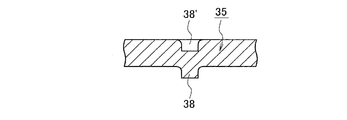
その非磁性板35には図7に拡大して示すように半抜き形状の嵌合突起38が現像ローラ30の長手方向に所定間隔を開けて複数個形成されている。その嵌合突起38は円柱形状である。その非磁性板35の嵌合突起38の根元部にはこの嵌合突起38を取り巻くようにして環状溝39が形成されている。
As shown in an enlarged view in FIG. 7, the
磁性板36は図8に拡大して示すように非磁性板35の長手方向に沿って長く延び、磁性板36にはその嵌合突起38に対応する嵌合穴40が形成されている。この嵌合穴40の穴径は嵌合突起38の直径よりも若干大きく、磁性板36の非磁性板35へのセットの容易化が図られている。その磁性板36はその長手方向両端部41に突き出し部42、42が形成されている。
As shown in an enlarged view in FIG. 8, the
磁性板36の両端部分では磁力が集中するため、この磁力集中による現像剤9の過剰吸引により、現像剤9が磁性板36の中央部分よりも両端部分の方が過剰に供給されるのを規制するためである。
Since magnetic force concentrates at both ends of the
その非磁性板35への嵌合突起38の形成は、例えば、図9に示す金型43を用いて行う。その金型43はダイプレート44、ポンチプレート45、ストリッパー45’、胴付きプレート45”を有する。ポンチプレート45、ストリッパー45’、胴付きプレート45”から大略構成される上型はダイプレート44に対して上下方向に可動される。ダイプレート44には円筒形状のダイボタン46が非磁性板35の長手方向に対応する方向に間隔を開けて複数個設けられている。
The
このダイボタン46は突き出し端部46aを有し、この突き出し端部46aのダイプレート44の上面からの突き出し高さH(図10参照)は、約50ミクロンメートル程度とされている。ポンチプレート45には、図9に示すように、そのダイボタン46に対応して円柱形状の加工用ポンチ47が設けられている。非磁性板35は図9に示すようにダイプレート44にセットされ、ポンチプレート45、ストリッパー45’とダイプレート44とにより挟持されつつ加工用ポンチ47により加圧される。
The
これにより、図7に示すように、非磁性板35にはその加工用ポンチ47に臨む側の面でかつ加工用ポンチ47により加圧された部分に凹み38’が形成され、反対側の面でかつ加工用ポンチ47により加圧された部分がダイボタン46の筒内に向かって押し出され、半抜き形状の嵌合突起38が形成される。その嵌合突起38はダイボタン46の筒内に食い込むが、嵌合突起38には図10に拡大して示すバネ46a’とイジェクトピン46bとによりダイボタン46の筒内から抜け出る方向の力が作用する。前述の突き出し高さHは胴付プレート45”とストリッパー45’との距離hによって決定される。なお、その図10において、符号46cは止めネジである。
Accordingly, as shown in FIG. 7, the
そのダイボタン46の突き出し端部46aにより、環状溝39が形成される。このダイボタン46は、嵌合突起38の形状を整形する役割を果たし、図10に部分的に拡大して示すように円柱形状の嵌合突起38の根元部分がいびつに塑性変形することなく形成される。
An
これに対して、ダイボタン46をダイプレート44に設けない場合には、図11に部分的に拡大して示すように、嵌合突起38の根元部分がだれていびつに塑性変形する。従って、この実施例によれば、磁性板36のセット面となる嵌合突起38の形成側の面のいびつな塑性変形が防止される。磁性板36への嵌合穴40の形成は公知の打ち抜き金型により行う。
On the other hand, when the
非磁性板35への磁性板36の締結は、図12に示すカシメ金型48を用いて行う。このカシメ金型48はダイプレート49を有する下型48Aと、ポンチプレート50、ストリッパー50’を有する上型48Bとからなる。ポンチプレート50にはカシメ用ポンチ51が嵌合突起38に対応させて設けられている。
The
そのカシメ用ポンチ51には、その先端の形状が図13(a)に示す円錐形、図13(b)に示すV字形、図13(c)に示す菊座形のいずれのものをも用いることができるが、V字形のカシメ用ポンチ51を用いるのが最も望ましい。その理由については、後述する。そのV字形の角度は120度が望ましい。
As the
非磁性板35をその嵌合突起38が上方を向くようにしてダイプレート49にセットする。ついで、磁性板36の嵌合穴40を嵌合突起38に嵌合させることにより、磁性板36を非磁性板35にセットする。ついで、上型48Bを下降させる。これにより、非磁性板35と磁性板36とはストリッパー50’により加圧挟持される。ついで、カシメ用ポンチ51が嵌合突起38の頭部38aに当接し、頭部38aが二分するように圧潰され、その頭部38aに図14、図15に拡大して示すように圧潰溝52が形成される。
The
その圧潰溝52の延びる方向は非磁性板35の長手方向に対して直交する方向が望ましい。というのは、圧潰溝52の延びる方向を非磁性板35の延びる方向と同方向に形成することにすると、図16に示すように、頭部38aの圧潰の際に塑性変形力Fが稜線10に向かう方向に主として加わることとなり、稜線10の直線度に影響を与える可能性が高いからである。言い換えると、非磁性板35の偏肉の方向が稜線10に向かう方向となるから、稜線10の直線度が劣化する。
The direction in which the crushing
これに対して、圧潰溝52の延びる方向を非磁性板35の延びる方向と直交する方向に形成すると、図17に示すように、頭部38aの圧潰の際に塑性変形力Fが主として稜線10と平行な方向に加わることとなり、稜線10の直線度に影響を与える可能性が低くなるからである。
On the other hand, when the direction in which the crushing
なお、ここで、稜線10とは非磁性板35を剪断加工により形成する際の剪断面側の縁、すなわち、剪断側の面とは嵌合突起38が形成されている側の面をいう。非磁性板35の破断面側の縁は破断の際に不揃いで凹凸が大きいので、真直度の測定に不向きだからである。
Here, the
その磁性板36の嵌合穴40の周辺部は、図14に示すように環状溝39の存在する方向に変形され、磁性板36はその全面が非磁性板35に密着する方向に押しつけられる。
これにより、非磁性板35と磁性板36との隙間53に現像剤9が侵入して現像剤9が非磁性板35と磁性板36との隙間53(図5参照)に溜まるのが防止される。
The peripheral portion of the
This prevents the developer 9 from entering the
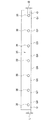
その非磁性板35の稜線10の真直度を稜線10から嵌合突起38の中心までの距離L、嵌合突起38の直径Φ、嵌合突起の高さH’、非磁性板35の厚さtを変えて測定して得られた結果を以下に説明する。
The straightness of the
図18から図21は非磁性板35の厚さtを2.0mmとし、嵌合突起38の直径Φを2mm、3mm、4mm、5mmに形成し、嵌合突起38の高さH’を厚さtの1/5、1/4、1/3、1/2に変化させ、かつ、嵌合突起38の中心から稜線10までの距離Lを嵌合突起38の直径Φの1倍、1.5倍、2倍、2.5倍に変化させて得られた真直度のグラフであり、横軸はその稜線10から中心までの距離Lであり、縦軸は真直度である。
18 to 21, the thickness t of the
図22から図25は非磁性板35の厚さtを1.5mmとし、嵌合突起38の直径Φを2mm、3mm、4mm、5mmに形成し、嵌合突起28の高さH’を厚さtの1/6.6、1/5、1/4、1/2.5に変化させ、かつ、嵌合突起38の中心から稜線10までの距離Lを嵌合突起38の直径Φの1倍、1.5倍、2倍、2.5倍に変化させて得られた真直度のグラフであり、横軸はその稜線10から中心までの距離Lであり、縦軸は真直度である。
22 to 25, the thickness t of the
ここで、その真直度は図26に示すように非磁性板35の両端部を基準点Oにして、非磁性板25の長手方向に所定間隔を開けて複数個の測定点Q1〜Q8を設定し、このQ1〜Q8の基準点Oに対する矢印方向の凹凸量ΔLで評価した。図18〜図25に示すグラフはその測定点Q1〜Q8における凹凸量ΔLの最大値である。
Here, the straightness is set at a plurality of measurement points Q1 to Q8 at predetermined intervals in the longitudinal direction of the
その図18ないし図25から見てとれるように、稜線10から嵌合突起38の中心までの距離Lを嵌合突起38の直径Φの2倍以上に設定すると、真直度0.05mm以下を実現できて好ましい。また、この実施例によれば、稜線10から嵌合突起38の中心までの距離Lを嵌合突起38の直径Φの2倍以上に設定すれば稜線10の直角度を保証できるので、磁性板36の長手方向と直交する方向の幅Wを狭くすることができ、磁性材料の節約、磁気力の大きさをコントロールできることになって望ましい。
As can be seen from FIGS. 18 to 25, when the distance L from the
なお、図18ないし図21と、図22ないし図25とを較べて見ると、非磁性板35の厚さtが薄い方が真直度が良好な結果が得られているが、これは非磁性板35が薄い方がこの非磁性板35をL字形状に折り曲げる際に折り曲げやすく、非磁性板35に加わる歪み変形が小さいと考えられるからである。
18 to 21 and FIG. 22 to FIG. 25 show that the straightness is better when the thickness t of the
この磁性板35に非磁性板36をカシメにより組み付けた場合にも同様に真直度0.05mm以下の結果を得ることができた。
Even when the
また、30mm間隔で嵌合突起38が形成された非磁性板35に磁性板36をカシメ加工により締結して形成した現像剤規制部材31を、A4用紙に1分間60枚のプリントが可能な画像形成装置に取り付けて、画像評価、耐久試験を行った。
Further, the
その結果、現像剤規制部材31に起因する画像異常の発生は見られなかった。また、600000枚相当の耐久試験を行ったが、磁性板の剥離や変形も見られず、非磁性板35と磁性板36とのカシメによる締結は、信頼性の高い締結手段であることが確認された。
As a result, no abnormality in the image due to the
更に、金型43を用いて非磁性板35に一度に複数個の半抜き形状の嵌合突起38を形成でき、カシメ金型48を用いてその複数個の嵌合突起38を同時にカシメることができることになり、非磁性板35と磁性板36とのカシメ締結加工時間は、現像剤規制部材31について1個当たり約5秒であり、加工時間も短縮でき、しかも現像剤規制部材31の製造工程の全てについてプレス加工を採用することができ、在庫管理、物流管理に貢献できるメリットもある。
Further, a plurality of half-drawn
以上、発明の実施の形態について説明したが本発明は、これに限らず以下のものを含むものである。
(1)発明の実施の形態では、非磁性板35に半抜き形状の嵌合突起38を形成し、磁性板36に嵌合突起38に嵌合する嵌合穴40を形成することにしたが、磁性板36に半抜き形状の嵌合突起を形成し、非磁性板35に嵌合突起に嵌合する嵌合穴を形成する構成とすることもできる。
(2)発明の実施の形態では、非磁性板35に半抜き形状の嵌合突起38を形成し、磁性板36に嵌合突起38に嵌合する嵌合穴40を形成し、嵌合突起38をカシメる構成としたが、嵌合突起38を嵌合穴40に軽く圧入する構成として、磁性板36を非磁性板35に取り付ける構成とすることもできる。
(3)非磁性板35に磁性板36の位置決めピン(図示を略す)を設ける構成としても良い。
(4)図13(c)に示す菊座型ポンチ51を用いた場合には、その圧潰溝52は図27に示すように、Y字形状を呈する構成とするのが望ましい。
(5)図28(a)に示すように、磁性板36の穴部40の周壁に鋭角状切片部40xを形成する構成、又は、図28(b)に示すように、磁性板36の穴部40の周壁に放射状切り込み条yを入れて放射切り込み片部40zを形成する構成として、嵌合突起38をカシメたときに、鋭角状切片部40x又は放射状切り込み片部40zを環状溝39に向けて変形しやすくし、磁性板36の全体としてのカシメによる応力変形を緩和する効果を与えることもできる。
(6)図29(a)に示すように、非磁性板35に長手方向に延びる半抜き形状の隆起条部35xを形成し、磁性板36に図29(b)に示すようにこの隆起条部35xに嵌合する長穴36xを形成し、隆起条部35xを長穴36xに嵌合させて、図29(c)に示すように、隆起条部35xの長手方向に間隔を開けてカシメ部35yを形成することにより、磁性板36を非磁性板35に取り付ける構成とすることもできる。
As mentioned above, although embodiment of invention was described, this invention is not restricted to this but includes the following.
(1) In the embodiment of the invention, the half-cut
(2) In the embodiment of the invention, the
(3) The
(4) When the
(5) As shown in FIG. 28A, a configuration in which an acute-angled
(6) As shown in FIG. 29 (a), a
この構成によれば、カシメ部35yの長手方向位置、間隔、個数を柔軟に選択できるという効果を奏する。
(7)非磁性板35としてプラスチックス材料を使用し、この非磁性板35に図30(a)に示すように嵌合突起38を形成し、図30(b)に示す磁性板36をこの嵌合突起38に嵌合させ、図30(c)に示す超音波ホーン60を用いて嵌合突起38の頭部を溶融させることにより磁性板36を非磁性板35に取り付ける構成とすることもできる。
According to this structure, there exists an effect that the longitudinal direction position, space | interval, and number of crimping
(7) A plastic material is used as the
この場合に、穴部40の周壁に放射状切り込み条を形成すれば、嵌合突起38の溶融部が放射状切り込み条に浸入するので、非磁性板35と磁性板36との結合強度の向上を図ることができる。
In this case, if a radial notch is formed on the peripheral wall of the
この構成によれば、非磁性板として金属製板を用いなくとも現像剤規制部材を製作できる。 According to this configuration, the developer regulating member can be manufactured without using a metal plate as the nonmagnetic plate.
このように、一の長尺状板又は一の長尺状板とは厚さが異なる他の長尺状板としての非磁性板35に嵌合突起38を形成し、一の長尺状板とは厚さが異なる他の長尺状板又は一の長尺板としての磁性板36に嵌合突起38に嵌合される嵌合穴40を形成し、嵌合突起38と嵌合穴40とを嵌合させ、嵌合突起38をカシメることにより結合板としての現像剤規制部材を形成する構成とすることもできる。
In this way, a
なお、結合板は、必ずしも現像剤規制部材に用いられるものに限られるものではなく、この現像剤規制部材と同様の機能を有するもの、例えば、スクレーパにも用いることができる。この場合には、双方の長尺状板として非磁性の金属製板を用いても良い。 Note that the coupling plate is not necessarily limited to that used for the developer regulating member, and can be used for a scraper that has the same function as the developer regulating member. In this case, a nonmagnetic metal plate may be used as both long plates.
30…現像ローラ
31…現像剤規制部材
32…マグネットローラ
35…非磁性板
36…磁性板
38…嵌合突起
40…嵌合穴
30 ... Developing
Claims (10)
Priority Applications (6)
| Application Number | Priority Date | Filing Date | Title |
|---|---|---|---|
| JP2004376741A JP4381970B2 (en) | 2004-09-30 | 2004-12-27 | Developer regulating member, method for producing developer regulating member, developing machine using the same, and image forming apparatus or printer using the developing machine |
| EP05768587.7A EP1812827B1 (en) | 2004-09-30 | 2005-08-01 | Developer-controlling member, manufacturing method thereof, developing machine using the developer-controlling member, image forming apparatus or printer using the developing machine, and jointed plate |
| CNB2005800410912A CN100483266C (en) | 2004-09-30 | 2005-08-01 | Developer-controlling member, manufacturing method thereof, developing machine using the developer-controlling member, image forming apparatus or printer using the developing machine, and jointed plat |
| US11/576,123 US8019257B2 (en) | 2004-09-30 | 2005-08-01 | Developer-controlling member, manufacturing method thereof, developing machine using the developer-controlling member, image forming apparatus or printer using the developing machine, and jointed plate |
| PCT/JP2005/014464 WO2006038375A1 (en) | 2004-09-30 | 2005-08-01 | Developer-controlling member, manufacturing method thereof, developing machine using the developer-controlling member, image forming apparatus or printer using the developing machine, and jointed plate |
| NO20071737A NO338933B1 (en) | 2004-09-30 | 2007-04-02 | Developer-controlling device, manufacture thereof, developing machine using the developer-controlling device, image forming apparatus or printer using the developing machine, and articulated plate |
Applications Claiming Priority (2)
| Application Number | Priority Date | Filing Date | Title |
|---|---|---|---|
| JP2004286288 | 2004-09-30 | ||
| JP2004376741A JP4381970B2 (en) | 2004-09-30 | 2004-12-27 | Developer regulating member, method for producing developer regulating member, developing machine using the same, and image forming apparatus or printer using the developing machine |
Publications (2)
| Publication Number | Publication Date |
|---|---|
| JP2006126764A JP2006126764A (en) | 2006-05-18 |
| JP4381970B2 true JP4381970B2 (en) | 2009-12-09 |
Family
ID=36142460
Family Applications (1)
| Application Number | Title | Priority Date | Filing Date |
|---|---|---|---|
| JP2004376741A Expired - Fee Related JP4381970B2 (en) | 2004-09-30 | 2004-12-27 | Developer regulating member, method for producing developer regulating member, developing machine using the same, and image forming apparatus or printer using the developing machine |
Country Status (6)
| Country | Link |
|---|---|
| US (1) | US8019257B2 (en) |
| EP (1) | EP1812827B1 (en) |
| JP (1) | JP4381970B2 (en) |
| CN (1) | CN100483266C (en) |
| NO (1) | NO338933B1 (en) |
| WO (1) | WO2006038375A1 (en) |
Families Citing this family (7)
| Publication number | Priority date | Publication date | Assignee | Title |
|---|---|---|---|---|
| JP4908120B2 (en) | 2006-09-07 | 2012-04-04 | 株式会社リコー | Developer regulating blade structure, developing machine using the same, printer using the developing machine, and image forming apparatus using the developing machine |
| JP5006145B2 (en) | 2007-09-19 | 2012-08-22 | 株式会社リコー | Manufacturing method of developer regulating member |
| JP5176508B2 (en) | 2007-12-04 | 2013-04-03 | 株式会社リコー | Fastening structure, blade structure, developing device, and image forming apparatus |
| JP5625865B2 (en) * | 2010-12-16 | 2014-11-19 | 株式会社リコー | Fixing apparatus and image forming apparatus |
| KR101896052B1 (en) * | 2012-04-19 | 2018-09-06 | 에이치피프린팅코리아 주식회사 | developing device and electrophotographic image forming apparatus using the same |
| US10288313B2 (en) * | 2015-12-25 | 2019-05-14 | Noritz Corporation | Gas supply manifold and production method of gas supply manifold |
| JP7073818B2 (en) * | 2018-03-19 | 2022-05-24 | 株式会社リコー | Develop device, process cartridge unit and image forming device |
Family Cites Families (18)
| Publication number | Priority date | Publication date | Assignee | Title |
|---|---|---|---|---|
| JPS58194045A (en) | 1982-05-10 | 1983-11-11 | Fuji Xerox Co Ltd | Frame of copying machine |
| JPH02160123A (en) | 1988-12-14 | 1990-06-20 | Matsushita Electric Ind Co Ltd | Press working method |
| JP2926597B2 (en) | 1989-08-08 | 1999-07-28 | 株式会社ニコン | Automatic light control device for camera |
| CA2089121C (en) | 1992-03-09 | 1998-08-04 | Steven J. Brox | Diamond film cutting tool |
| JPH06282122A (en) * | 1992-04-16 | 1994-10-07 | Canon Inc | Blade member, method for attaching blade member, process cartridge, method for assembling process cartridge and image forming device |
| JPH05337572A (en) | 1992-06-12 | 1993-12-21 | Brother Ind Ltd | Joining part of metal member |
| JPH08160742A (en) | 1994-12-01 | 1996-06-21 | Seiko Epson Corp | Developing device |
| JPH08190327A (en) | 1995-01-12 | 1996-07-23 | Bando Chem Ind Ltd | Production of blade |
| JPH11179452A (en) | 1997-12-19 | 1999-07-06 | Ricoh Co Ltd | Method for burring binding, binding structure and burring forming punch |
| JP3677408B2 (en) * | 1998-04-20 | 2005-08-03 | 株式会社リコー | Image forming apparatus |
| JP2000121757A (en) | 1998-10-20 | 2000-04-28 | Citizen Watch Co Ltd | Coil winding core for clock, connection structure of circuit substrate, and its connection method |
| JP2001356595A (en) | 2000-04-10 | 2001-12-26 | Toyo Tire & Rubber Co Ltd | Toner regulating blade, its manufacturing method and method for fixing toner regulating blade |
| JP2001300658A (en) | 2000-04-27 | 2001-10-30 | Fujitsu Ten Ltd | Fastening structure of parts, and fastening structure of casing and cover |
| JP2002102955A (en) | 2000-09-28 | 2002-04-09 | Miyota Kk | Back cover fixing device and fixing method for wrist watch |
| JP3548558B2 (en) * | 2001-12-13 | 2004-07-28 | キヤノン株式会社 | Process cartridge and electrophotographic image forming apparatus |
| JP2004093672A (en) | 2002-08-29 | 2004-03-25 | Canon Inc | Developing device and image forming apparatus |
| JP2004191529A (en) * | 2002-12-10 | 2004-07-08 | Kyocera Mita Corp | Development device |
| JP5006145B2 (en) * | 2007-09-19 | 2012-08-22 | 株式会社リコー | Manufacturing method of developer regulating member |
-
2004
- 2004-12-27 JP JP2004376741A patent/JP4381970B2/en not_active Expired - Fee Related
-
2005
- 2005-08-01 EP EP05768587.7A patent/EP1812827B1/en not_active Not-in-force
- 2005-08-01 WO PCT/JP2005/014464 patent/WO2006038375A1/en active Application Filing
- 2005-08-01 US US11/576,123 patent/US8019257B2/en not_active Expired - Fee Related
- 2005-08-01 CN CNB2005800410912A patent/CN100483266C/en not_active Expired - Fee Related
-
2007
- 2007-04-02 NO NO20071737A patent/NO338933B1/en not_active IP Right Cessation
Also Published As
| Publication number | Publication date |
|---|---|
| JP2006126764A (en) | 2006-05-18 |
| WO2006038375A1 (en) | 2006-04-13 |
| EP1812827B1 (en) | 2013-07-10 |
| NO338933B1 (en) | 2016-10-31 |
| NO20071737L (en) | 2007-07-23 |
| CN101069134A (en) | 2007-11-07 |
| EP1812827A1 (en) | 2007-08-01 |
| EP1812827A4 (en) | 2011-10-19 |
| CN100483266C (en) | 2009-04-29 |
| US20080069597A1 (en) | 2008-03-20 |
| US8019257B2 (en) | 2011-09-13 |
Similar Documents
| Publication | Publication Date | Title |
|---|---|---|
| EP1898273B1 (en) | Developer Amount Regulation Blade Structure | |
| EP1812827B1 (en) | Developer-controlling member, manufacturing method thereof, developing machine using the developer-controlling member, image forming apparatus or printer using the developing machine, and jointed plate | |
| US9352381B2 (en) | Lead pin rectifying apparatus and lead pin rectifying method | |
| EP3550379A1 (en) | Embossed component and housing and image forming apparatus including same | |
| US7464467B2 (en) | Method for manufacturing sheet-conveying roller | |
| JP4541135B2 (en) | Developer regulating member | |
| JP4966516B2 (en) | Drilling device and drilling mold for this drilling device | |
| US6433674B2 (en) | Electromagnetic sound generator | |
| JP2000246363A (en) | Die cut processing substrate, die cut substrate, and manufacture of die cut substrate | |
| JP6874316B2 (en) | Developer | |
| US6729782B2 (en) | Wire dot printer head | |
| JP2021144074A (en) | Fixation device | |
| JP2000326475A (en) | Plate-making device | |
| JP6256009B2 (en) | Fixing apparatus and image forming apparatus | |
| KR101978390B1 (en) | Cleaning blade for photosensitive and method for producing same, image forming apparatus | |
| JP2006145759A (en) | Image forming apparatus | |
| US7585124B2 (en) | Armature structure and dot head | |
| JP6236937B2 (en) | Print head and image forming apparatus | |
| JP3467524B2 (en) | Nib | |
| JP6624906B2 (en) | Scanning optical device and image forming apparatus | |
| JPH04283786A (en) | Manufacture of cleaning blade | |
| JP2006231441A (en) | Blanking die | |
| JP2004301940A (en) | Laser scanning optical device | |
| JPH0545714U (en) | Cartridge mounting structure | |
| JP2006231440A (en) | Blanking die |
Legal Events
| Date | Code | Title | Description |
|---|---|---|---|
| A621 | Written request for application examination |
Free format text: JAPANESE INTERMEDIATE CODE: A621 Effective date: 20071127 |
|
| A131 | Notification of reasons for refusal |
Free format text: JAPANESE INTERMEDIATE CODE: A131 Effective date: 20090414 |
|
| A521 | Written amendment |
Free format text: JAPANESE INTERMEDIATE CODE: A523 Effective date: 20090421 |
|
| A131 | Notification of reasons for refusal |
Free format text: JAPANESE INTERMEDIATE CODE: A131 Effective date: 20090616 |
|
| A521 | Written amendment |
Free format text: JAPANESE INTERMEDIATE CODE: A523 Effective date: 20090723 |
|
| TRDD | Decision of grant or rejection written | ||
| A01 | Written decision to grant a patent or to grant a registration (utility model) |
Free format text: JAPANESE INTERMEDIATE CODE: A01 Effective date: 20090915 |
|
| A01 | Written decision to grant a patent or to grant a registration (utility model) |
Free format text: JAPANESE INTERMEDIATE CODE: A01 |
|
| A61 | First payment of annual fees (during grant procedure) |
Free format text: JAPANESE INTERMEDIATE CODE: A61 Effective date: 20090916 |
|
| FPAY | Renewal fee payment (event date is renewal date of database) |
Free format text: PAYMENT UNTIL: 20121002 Year of fee payment: 3 |
|
| R150 | Certificate of patent or registration of utility model |
Free format text: JAPANESE INTERMEDIATE CODE: R150 |
|
| FPAY | Renewal fee payment (event date is renewal date of database) |
Free format text: PAYMENT UNTIL: 20131002 Year of fee payment: 4 |
|
| LAPS | Cancellation because of no payment of annual fees |