JP4372191B2 - Charging / discharging device, display device, plasma display panel, and charging / discharging method - Google Patents
Charging / discharging device, display device, plasma display panel, and charging / discharging method Download PDFInfo
- Publication number
- JP4372191B2 JP4372191B2 JP2007504579A JP2007504579A JP4372191B2 JP 4372191 B2 JP4372191 B2 JP 4372191B2 JP 2007504579 A JP2007504579 A JP 2007504579A JP 2007504579 A JP2007504579 A JP 2007504579A JP 4372191 B2 JP4372191 B2 JP 4372191B2
- Authority
- JP
- Japan
- Prior art keywords
- switch
- groups
- electrodes
- path forming
- terminal
- Prior art date
- Legal status (The legal status is an assumption and is not a legal conclusion. Google has not performed a legal analysis and makes no representation as to the accuracy of the status listed.)
- Expired - Fee Related
Links
Images


Classifications
-
- G—PHYSICS
- G09—EDUCATION; CRYPTOGRAPHY; DISPLAY; ADVERTISING; SEALS
- G09G—ARRANGEMENTS OR CIRCUITS FOR CONTROL OF INDICATING DEVICES USING STATIC MEANS TO PRESENT VARIABLE INFORMATION
- G09G3/00—Control arrangements or circuits, of interest only in connection with visual indicators other than cathode-ray tubes
- G09G3/20—Control arrangements or circuits, of interest only in connection with visual indicators other than cathode-ray tubes for presentation of an assembly of a number of characters, e.g. a page, by composing the assembly by combination of individual elements arranged in a matrix no fixed position being assigned to or needed to be assigned to the individual characters or partial characters
- G09G3/22—Control arrangements or circuits, of interest only in connection with visual indicators other than cathode-ray tubes for presentation of an assembly of a number of characters, e.g. a page, by composing the assembly by combination of individual elements arranged in a matrix no fixed position being assigned to or needed to be assigned to the individual characters or partial characters using controlled light sources
- G09G3/28—Control arrangements or circuits, of interest only in connection with visual indicators other than cathode-ray tubes for presentation of an assembly of a number of characters, e.g. a page, by composing the assembly by combination of individual elements arranged in a matrix no fixed position being assigned to or needed to be assigned to the individual characters or partial characters using controlled light sources using luminous gas-discharge panels, e.g. plasma panels
- G09G3/288—Control arrangements or circuits, of interest only in connection with visual indicators other than cathode-ray tubes for presentation of an assembly of a number of characters, e.g. a page, by composing the assembly by combination of individual elements arranged in a matrix no fixed position being assigned to or needed to be assigned to the individual characters or partial characters using controlled light sources using luminous gas-discharge panels, e.g. plasma panels using AC panels
- G09G3/296—Driving circuits for producing the waveforms applied to the driving electrodes
- G09G3/2965—Driving circuits for producing the waveforms applied to the driving electrodes using inductors for energy recovery
-
- G—PHYSICS
- G09—EDUCATION; CRYPTOGRAPHY; DISPLAY; ADVERTISING; SEALS
- G09G—ARRANGEMENTS OR CIRCUITS FOR CONTROL OF INDICATING DEVICES USING STATIC MEANS TO PRESENT VARIABLE INFORMATION
- G09G2310/00—Command of the display device
- G09G2310/06—Details of flat display driving waveforms
- G09G2310/066—Waveforms comprising a gently increasing or decreasing portion, e.g. ramp
-
- G—PHYSICS
- G09—EDUCATION; CRYPTOGRAPHY; DISPLAY; ADVERTISING; SEALS
- G09G—ARRANGEMENTS OR CIRCUITS FOR CONTROL OF INDICATING DEVICES USING STATIC MEANS TO PRESENT VARIABLE INFORMATION
- G09G2330/00—Aspects of power supply; Aspects of display protection and defect management
- G09G2330/02—Details of power systems and of start or stop of display operation
Description
本発明は、キャパシタンスに蓄積された電気的エネルギの回収に関し、特に、プラズマ・パネル・ディスプレイ(PDP)の画面を構成するセルに形成される容量にパルス状電圧を印加することによって蓄積される電荷を回収する充放電装置、プラズマ・ディスプレイ・パネルおよび充放電の方法に関する。 The present invention relates to recovery of electrical energy stored in a capacitance, and more particularly, a charge stored by applying a pulse voltage to a capacitor formed in a cell constituting a screen of a plasma panel display (PDP). The present invention relates to a charge / discharge device, a plasma display panel, and a charge / discharge method.
対をなすPDPの表示電極間にサステイン・パルス電圧を印加することによってその表示電極間の容量(キャパシタンス)に電荷すなわち電気的エネルギが蓄積される。その電気的エネルギを回収キャパシタを用いて回収する技術が知られている。そのキャパシタに回収された電気的エネルギは、次の表示電極間へのサステイン・パルス電圧の印加に用いられる。 By applying a sustain pulse voltage between the display electrodes of a pair of PDPs, electric charge, that is, electric energy is accumulated in the capacitance (capacitance) between the display electrodes. A technique for recovering the electrical energy using a recovery capacitor is known. The electric energy recovered by the capacitor is used for applying a sustain pulse voltage between the next display electrodes.
1999年12月10日付けで公開された特開平11−338416号公報(A)には、プラズマ・ディスプレイ・パネルの駆動方法が記載されている。この駆動方法では、インダクタを用いずに高速に電極の電位を推移させ、複数のセルに対する電圧印加のパターンに係わらず安定した電力回収を行って消費電力を低減する。この駆動方法では、電力回収用の容量素子の第1端子を電極に接続するとともに、その容量素子の第2端子を、第2電位ラインGNDより低く且つ第2電位ラインとの電位差が第1電位ラインVsと第2電位ラインGNDの電位差より大きい電位(−2Vs)に一時的に固定することによって電力回収を行う。充電状態のその容量素子の第1端子をその電極に接続するとともに、第1端子の電位が第1電位ラインよりも高くなるように第2端子の電位を一時的に固定することによってセルの充電を行う。アドレス電極は複数のグループに分けられ、グループ毎にアドレスドライバLSIと電力回収回路が設けられるようにしてもよい。それによって、電力回収回路1個当たりのアドレス電極間静電容量の和を小さくすることができ、容量充放電の速度を早めることができる。
1999年12月10日付けで公開された特開平11−338418号公報(A)には、プラズマ・ディスプレイ・パネルの駆動方法およびプラズマ・ディスプレイ・パネル装置が記載されている。この装置では、複数のブロックに分割されたPDPに低コストの無効電力回収回路が設けられる。2つのX電極がFETとコイルとを介して接続され、2つのY電極がFETとコイルとを介して接続され、第1のX電極と第2のY電極がFETとコイルを介して接続され、第2のY電極と第1のX電極がFETとコイルを介して接続される。第1と第2のX電極間のコイルを介する経路を通じて、対をなす第1のX電極と第1のY電極の間の容量に貯えられていたエネルギを別の対をなす第2のX電極と第2のY電極の間の容量に放出する。エネルギ放出の途中において第2のX電極の電位が電位Vsに達する。第1のX電極は接地される。
2000年12月8日付けで公開された特開2000−338934号公報(A)には、容量性負荷の駆動方法が記載されている。この駆動方法では、電極対の各電極電位を2値制御する容量性負荷の駆動において、電極対の一方の電極を、トランスの1次巻線を介してバイアス電位ラインに接続し、且つトランスの2次巻線を介して接地電位ラインに接続するとともに、当該電極対の他方の電極を接地電位ラインに接続し、電極対の電極間の容量を充電する。
2003年3月14日付けで公開された特開2003−76321号公報(A)には、プラズマ・ディスプレイ・パネル表示装置が記載されている。この表示装置では、一対の表示電極において、維持期間では一方の電極の立ち上がり期間から他方の電極の立ち下がり期間を時間的に重ねる駆動波形プロセスとする。パルス波形の立ち上がり、立ち下がりの勾配を急にせずに一対の表示電極に印加する維持パルスの間隔を短くする。
回収された電気的エネルギを蓄積している回収用キャパシタによってサステイン・パルスをインダクタを介してPDPの表示電極に印加すると、サステイン・パルスの立ち上がり時間は長くなる傾向がある。そのインダクタは、表示電極に共振的に電気的エネルギを供給するために所要の大きさのインダクタンスを必要とする。そのインダクタのインダクタンスを小さくすると電気的エネルギの回収効率が低下する。 When the sustain pulse is applied to the display electrode of the PDP through the inductor by the recovery capacitor that stores the recovered electrical energy, the rise time of the sustain pulse tends to be long. The inductor requires an inductance having a required magnitude in order to resonately supply electric energy to the display electrode. If the inductance of the inductor is reduced, the electrical energy recovery efficiency is lowered.
発明者たちは、PDPの駆動において、表示電極間に印加するパルスの幅をより短くし、表示電極へのパルス印加の開始から放電までの遅延をより短くするためには、電気的エネルギの回収効率を低下させることなく表示電極に印加されるパルスの立ち上がり時間を短くすることが望ましい、また、表示電極に印加されるパルスの立ち上がり時間を長くすることなく電気的エネルギの回収効率を高くすることが望ましい、と認識した。 In order to reduce the width of the pulse applied between the display electrodes and to further shorten the delay from the start of pulse application to the display electrode in the driving of the PDP, the inventors have recovered electric energy. It is desirable to shorten the rise time of the pulse applied to the display electrode without reducing the efficiency, and increase the recovery efficiency of electrical energy without increasing the rise time of the pulse applied to the display electrode. Recognized that is desirable.
本発明の目的は、短い立ち上がり時間のパルスを電極に印加する回路を実現することである。 An object of the present invention is to realize a circuit that applies a pulse having a short rise time to an electrode.
本発明の別の目的は、電極へのパルス印加の開始から放電までの遅延を短くすることである。 Another object of the present invention is to shorten the delay from the start of pulse application to the electrode until discharge.
本発明のさらに別の目的は、電極へ印加するパルスの幅を小さくすることである。 Yet another object of the present invention is to reduce the width of the pulse applied to the electrode.
本発明のさらに別の目的は、充放電キャパシタンスに蓄積された電気的エネルギの回収効率を高くすることである。 Yet another object of the present invention is to increase the recovery efficiency of the electrical energy stored in the charge / discharge capacitance.
本発明の特徴によれば、充放電装置は、電圧を印加することによって、複数g個のグループに分けられた複数のキャパシタンスを充放電し、さらに、共通導体電位に一端子が結合された電気的エネルギ回収用の回収用キャパシタと、そのg個のグループにそれぞれ対応付けられた複数の共振インダクタと、を具える。その複数の共振インダクタのそれぞれの一方の端子はそのg個のそれぞれのグループのキャパシタンスに結合され、その複数の共振インダクタのそれぞれの他方の端子はその回収用キャパシタの他端子に結合される。その充放電装置は、さらに、その回収用キャパシタからg個の共振インダクタを介してそのg個のそれぞれのグループのキャパシタンスを充電する第1の経路形成手段と、そのg個のグループのキャパシタンスを放電させて、g個の共振インダクタンスをそれぞれ介してその回収用キャパシタに電気的エネルギを回収する第2の経路形成手段と、その第1と第2の経路形成手段を制御する制御手段と、を具える。 According to the characteristics of the present invention, the charging / discharging device charges / discharges a plurality of capacitances divided into a plurality of groups of g by applying a voltage, and further, an electrical device having one terminal coupled to a common conductor potential. And a plurality of resonant inductors respectively associated with the g groups. One terminal of each of the plurality of resonant inductors is coupled to the capacitance of each of the g groups, and the other terminal of each of the plurality of resonant inductors is coupled to the other terminal of the recovery capacitor. The charging / discharging apparatus further discharges the capacitances of the g groups from the recovery capacitor through first resonant inductors, charging the capacitances of the g groups, respectively. And a second path forming means for recovering electrical energy to the recovery capacitor through g resonance inductances, and a control means for controlling the first and second path forming means. Yeah.
また、本発明は、上述の充放電装置を含む表示装置およびプラズマ・ディスプレイ・パネルに関する。 The present invention also relates to a display device and a plasma display panel including the above-described charging / discharging device.
また、本発明は、上述の充放電装置の機能を実現する充放電の方法に関する。 Moreover, this invention relates to the method of charging / discharging which implement | achieves the function of the above-mentioned charging / discharging apparatus.
本発明によれば、電極に印加するパルスの立ち上がり時間を短くすることができ、電極に印加するパルスの幅を小さくすることができ、所定期間内により多数のパルスの位置を確保することによって表示装置の表示品質を向上させることができ、また、充放電キャパシタンスに蓄積された電気的エネルギの回収効率を高くすることができる。 According to the present invention, the rise time of the pulse applied to the electrode can be shortened, the width of the pulse applied to the electrode can be reduced, and the display can be achieved by ensuring the position of a larger number of pulses within a predetermined period. The display quality of the apparatus can be improved, and the recovery efficiency of the electrical energy accumulated in the charge / discharge capacitance can be increased.
本発明の実施形態を、図面を参照して説明する。図面において、同様の構成要素には同じ参照番号が付されている。 Embodiments of the present invention will be described with reference to the drawings. In the drawings, similar components are given the same reference numerals.
図1は、本発明の実施形態による、典型例の表示装置60の構成を示している。表示装置60は、n×m個のセルのアレイからなる表示面を有する3電極面放電型のPDP10と、セルのアレイを選択的に発光させるためのドライブ・ユニット50とを具えており、例えばテレビジョン受像機、コンピュータ・システムのモニタ等に利用される。 FIG. 1 shows a configuration of a typical display device 60 according to an embodiment of the present invention. The display device 60 includes a three-electrode surface
PDP10では、表示放電を生じさせるための電極対を構成する表示電極XおよびY(X1,Y1,...Xj,Yj,...Xm,Ym)が平行に配置され、これら表示電極XおよびYと直交するようにアドレス電極A(A1,...Ai,...Am)が配置されている。表示電極Xはサステイン(維持)電極であり、表示電極Yはスキャン(走査)電極である。表示電極XおよびYは、典型的には画面の行方向または水平方向に延び、アドレス電極Aは列方向または垂直方向に延びている。 In the
ドライブ・ユニット50は、ドライバ制御回路51、データ変換回路52、電源回路53、X電極ドライバ回路またはXドライバ回路61、Y電極ドライバ回路またはYドライバ回路64、およびアドレス電極ドライバ回路またはAドライバ回路68を含んでおり、場合によってROMを含み得る集積回路の形態で実装される。ドライブ・ユニット50には、TVチューナまたはコンピュータのような外部装置からR,GおよびBの3原色の発光強度を示すフィールド・データDfが各種の同期信号とともに入力される。フィールド・データDfはデータ変換回路52の中のフィールドメモリに一時的に記憶される。データ変換回路52は、フィールド・データDfを階調表示のためのサブフィールド・データDsfに変換してAドライバ回路68に供給する。サブフィールド・データDsfは、1セル当たり1ビットの表示データの集合であって、その各ビットの値は該当する1つのサブフィールドSFにおける各セルの発光の要否を表す。 The
Xドライバ回路61は、PDP表示面を構成する複数のセルの壁電圧を均等にするために表示電極Xに初期化のための電圧を印加するリセット回路62と、セルに表示放電を生じさせるために表示電極Xにサステイン・パルスを印加するサステイン回路63とを含んでいる。Yドライバ回路64は、表示電極Yに初期化のための電圧を印加するリセット回路65と、アドレッシングにおいて表示電極Yにスキャンパルスを印加するスキャン回路66と、セルに表示放電を生じさせるために表示電極Yにサステイン・パルスを印加するサステイン回路67とを含んでいる。Aドライバ回路68は、表示データに応じてサブフィールド・データDsfによって指定されたアドレス電極Aにアドレスパルスを印加する。 The X driver circuit 61 includes a reset circuit 62 that applies a voltage for initialization to the display electrode X in order to equalize the wall voltages of a plurality of cells constituting the PDP display surface, and a display discharge in the cells. And a sustain
ドライバ制御回路51は、パルス電圧の印加およびサブフィールド・データDsfの転送を制御する。電源回路53はユニット内の所要部分に駆動電力を供給する。 The
1つのピクチャ(画面)は典型的には1フレーム期間で構成されており、インターレース型走査では1フレームが2つのフィールドで構成され、プログレッシブ型走査では1フレームが1つのフィールドで構成されている。PDP10による表示では、2値の発光制御によってカラー再現を行うために、典型的にはそのような1フィールド期間の入力画像の時系列の1つのフィールドFを所定数qのサブフィールドSFに分割する。典型的には、各フィールドFをq個のサブフィールドSFの集合に置き換える。しばしば、これらサブフィールドSFに順に20,21,22,...2q−1等の異なる重みを付けて各サブフィールドSFの表示放電の回数を設定する。サブフィールド単位の発光/非発光の組合せでR,GおよびBの各色毎にN(=1+21+22+...+2q−1)段階の輝度設定を行うことができる。このようなフィールド構成に合わせてフィールド転送周期であるフィールド期間Tfをq個のサブフィールド期間Tsfに分割し、各サブフィールドSFに1つのサブフィールド期間Tsfを割り当てる。さらに、サブフィールド期間Tsfを、初期化のためのリセット期間TR、アドレッシングのためのアドレス期間TA、および発光のための表示期間TSに分ける。典型的には、リセット期間TRおよびアドレス期間TAの長さが重みに係わらず一定であるのに対し、表示期間TSにおけるパルス数は重みが大きいほど多く、表示期間TSの長さは重みが大きいほど長い。この場合、サブフィールド期間Tsfの長さも、該当するサブフィールドSFの重みが大きいほど長い。One picture (screen) is typically composed of one frame period. In interlaced scanning, one frame is composed of two fields, and in progressive scanning, one frame is composed of one field. In the display by the
図2は、本発明の実施形態による、Xドライバ回路61、Yドライバ回路64およびAドライバ回路68の出力駆動電圧波形の概略的な駆動シーケンスを例示している。なお、図示の波形は一例であり、振幅、極性およびタイミングを様々に変更することができる。 FIG. 2 illustrates a schematic drive sequence of output drive voltage waveforms of the X driver circuit 61, the
リセット期間TR、アドレス期間TAおよびサステイン期間TSの順序は、q個のサブフィールドSFにおいて同じであり、駆動シーケンスはサブフィールドSF毎に繰り返される。各サブフィールドSFのリセット期間TRにおいては、全ての表示電極Xに対して負極性のパルスPrx1と正極性のパルスPrx2とを順に印加し、全ての表示電極Yに対して正極性のパルスPry1と負極性のパルスPry2とを順に印加する。パルスPrx1、Pry1およびPry2は微小放電が生じる変化率で振幅が漸増するランプ波形または鈍波パルスである。最初に印加されるパルスPrx1およびPry1は、前サブフィールドSFにおける発光/非発光に係わらず全てのセルに同一極性の適当な壁電圧を生じさせるために印加される。適度の壁電荷が存在するセルにパルスPrx2およびPry2を印加することにより、壁電圧を放電開始電圧とパルス振幅との差に相当する値に調整することができる。セルに加わる駆動電圧は、表示電極XおよびYに印加されるパルスの振幅の差を表す合成電圧である。 The order of the reset period TR, the address period TA, and the sustain period TS is the same in the q subfields SF, and the driving sequence is repeated for each subfield SF. In the reset period TR of each subfield SF, a negative pulse Prx1 and a positive pulse Prx2 are sequentially applied to all the display electrodes X, and a positive pulse Pry1 is applied to all the display electrodes Y. A negative pulse Pry2 is applied in order. The pulses Prx1, Pry1, and Pry2 are ramp waveforms or blunt waves that gradually increase in amplitude at the rate of change at which microdischarge occurs. The first applied pulses Prx1 and Pry1 are applied to generate appropriate wall voltages of the same polarity in all cells regardless of light emission / non-light emission in the previous subfield SF. By applying the pulses Prx2 and Pry2 to a cell having an appropriate wall charge, the wall voltage can be adjusted to a value corresponding to the difference between the discharge start voltage and the pulse amplitude. The drive voltage applied to the cell is a combined voltage representing the difference in the amplitude of the pulses applied to the display electrodes X and Y.
アドレス期間TAにおいては、発光させるセルのみに発光維持に必要な壁電荷を形成する。全ての表示電極Xおよび全ての表示電極Yを所定電位にバイアスした状態で、行選択期間(1行分のスキャン時間)毎に選択行に対応した表示電極Yに負極性のスキャンパルス−Vyを印加する。この行選択と同時にアドレス放電を生じさせるべき選択セルに対応したアドレス電極AのみにアドレスパルスVaを印加する。つまり、選択行jのm列分のサブフィールド・データDsfに基づいてアドレス電極A1〜Amの電位を2値制御する。選択セルでは表示電極Yとアドレス電極Aとの間の放電が生じる。そのアドレス放電がトリガとなって、その後の表示電極X−Y間の面放電が生じる。 In the address period TA, wall charges necessary for maintaining light emission are formed only in the cells that emit light. With all the display electrodes X and all the display electrodes Y biased to a predetermined potential, a negative scan pulse -Vy is applied to the display electrodes Y corresponding to the selected row for each row selection period (scanning time for one row). Apply. Simultaneously with this row selection, the address pulse Va is applied only to the address electrode A corresponding to the selected cell in which the address discharge is to be generated. That is, the potentials of the address electrodes A1 to Am are subjected to binary control based on the subfield data Dsf for m columns of the selected row j. In the selected cell, a discharge occurs between the display electrode Y and the address electrode A. The address discharge is a trigger, and subsequent surface discharge between the display electrodes XY occurs.
サステステイン期間TSにおいては、最初に全ての表示電極Yに対して所定極性(図の例では正極性)のサステイン・パルスPsを印加する。その後、表示電極Xと表示電極Yとに対して交互にサステイン・パルスPsを印加する。サステイン・パルスPsの振幅は維持電圧Vsである。サステイン・パルスPsの印加によって、所定の壁電荷が残存するセルにおいて面放電が生じる。サステイン・パルスPsの印加回数は、上述したようにサブフィールドSFの重みに対応する。なお、サステイン期間TS全体にわたって不要な対向放電を防止するために、アドレス電極Aをサステイン・パルスPsと同極性の電圧Vasにバイアスする。 In the sustain period TS, first, a sustain pulse Ps having a predetermined polarity (positive polarity in the illustrated example) is applied to all the display electrodes Y. Thereafter, the sustain pulse Ps is alternately applied to the display electrode X and the display electrode Y. The amplitude of the sustain pulse Ps is the sustain voltage Vs. By applying the sustain pulse Ps, a surface discharge occurs in a cell in which a predetermined wall charge remains. The number of times the sustain pulse Ps is applied corresponds to the weight of the subfield SF as described above. Note that the address electrode A is biased to the voltage Vas having the same polarity as the sustain pulse Ps in order to prevent unnecessary counter discharge throughout the sustain period TS.
図1において、各1対の表示電極XjとYjで形成されるキャパシタンスCは容量Cを有する。図1のサステイン回路63および67によって各1対の表示電極XjとYjの間に図2の2つの系列のサステイン・パルスPsの電圧Vsがそれぞれ印加される。 In FIG. 1, a capacitance C formed by each pair of display electrodes Xj and Yj has a capacitance C. The sustain
図3は、PDP10用のサステイン回路63および67に用いられる、電気的エネルギ回収すなわち電力回収機能を有する通常のパルス電力供給および回収回路11と、クランプ回路14とを示している。全n対の表示電極の合計容量または合計パネル容量Cpaは、全てのn対の表示電極XおよびYの間に形成された、例えば200nFのオーダの合計容量Cpa=nCを有する。 FIG. 3 shows a normal pulse power supply and
図3において、パルス電力供給および回収回路11は、n対の表示電極XおよびYの間の合計パネル容量Cpaより充分大きい容量Cr(例えばCpaの100倍以上)を有し一方の端子が接地点GNDに結合された電力回収キャパシタCrと、回収キャパシタCrに直列にそれぞれの一方の端子がスイッチSW1およびSW3をそれぞれ介して互いに逆極性で並列に結合されたダイオードD1およびD2と、ダイオードD1およびD2の他端子の接続点に一端子が結合され他端子が容量Cpaのn対の表示電極の各対の一方(XまたはY)に結合された共通の共振インダクタL1と、を含んでいる。共振インダクタL1のインダクタンスLは、典型的には200〜500nHである。 In FIG. 3, the pulse power supply and
クランプ回路14は、共振インダクタL1の他端子と一方の表示電極(XまたはY)との間の接続点にスイッチSW2を介して結合された所定の電圧Vsの定電圧源Vsを含み、その接続点をスイッチSW4を介して接地点GNDに結合する。 The
図3を参照すると、最初に回収キャパシタCrに概ね電圧Vs/2の電荷が蓄積されており、n対の表示電極の合計パネル容量Cpaには電荷が蓄積されていないものとする。従って、パネル容量Cpaすなわち各キャパシタンスCにおける電圧VCpaの値はゼロ(0)である。パルスPsの立ち上がりの開始において、スイッチSW1がターンオンすると、回収キャパシタからスイッチSW1、ダイオードD1および共振インダクタL1を介してn個のキャパシタンスCの合計パネル容量Cpa=nCに供給電流が流れ、電荷q〜CpaVsが合計パネル容量Cpaに蓄積され、パネル容量Cpaすなわち各キャパシタンスCの電圧VCpaが上昇し、パルスPsの立ち上がりが形成される。パネル容量Cpaの電圧VCpaがほぼピーク電圧Vpmaxに達したとき、クランプ回路14のスイッチSW2がターンオンされる。そのピーク電圧Vpmaxは電圧Vsより僅かに低い。その後、スイッチSW1がターンオフされる。クランプ回路14の電圧源Vsは、パネル容量Cpaの電圧を電圧Vsにクランプし、パネル容量Cpaを電圧Vsに維持する。クランプ回路14はパネル容量Cpaの電圧VCpaを所定の電圧Vsになるように補償する。その後、サステイン放電が生じ、スイッチSW2がターンオフされる。Referring to FIG. 3, it is assumed that charges of the voltage Vs / 2 are first accumulated in the recovery capacitor Cr, and no charges are accumulated in the total panel capacitance Cpa of n pairs of display electrodes. Therefore, the value of the panel capacitance Cpa, that is, the voltage V Cpa at each capacitance C is zero (0). When the switch SW1 is turned on at the start of the rise of the pulse Ps, the supply current flows from the recovery capacitor to the total panel capacitance Cpa = nC of the n capacitors C through the switch SW1, the diode D1, and the resonant inductor L1, and the charge q˜ CpaVs is accumulated in the total panel capacitance Cpa, the panel capacitance Cpa, that is, the voltage V Cpa of each capacitance C rises, and the rise of the pulse Ps is formed. Upon reaching a voltage V Cpa approximately peak voltage Vpmax of the panel capacitance Cpa, switch SW2 of the
パルスPsの立ち下がりの開始において、スイッチSW3がターンオンされると、合計パネル容量Cpから共振インダクタL1、ダイオードD2およびスイッチSW3を介して回収キャパシタCrに還流電流が流れ、電荷q〜CpaVsが回収キャパシタCrに追加的に蓄積され、パネル容量Cpaの電圧VCpaが下降し、パルスPsの立ち下がりが形成される。パネル容量Cpaの電圧VCpaが負方向のピーク電圧Vpminにほぼ達したとき、スイッチSW4がターンオンされる。そのピーク電圧Vpminは接地電位GNDまたは0Vより僅かに高い。その後、スイッチSW3がターンオフされる。クランプ回路14の接地点GNDは、パネル容量Cpaの電圧VCpaを接地電位GNDまたは0Vにクランプする。その後、スイッチSW4がターンオフされる。このようにして、回収キャパシタCrから合計パネル容量Cpaに供給された電荷すなわち電力の大部分が回収される。When the switch SW3 is turned on at the start of the fall of the pulse Ps, a return current flows from the total panel capacitance Cp to the recovery capacitor Cr via the resonant inductor L1, the diode D2, and the switch SW3, and the charges q to CpaVs are recovered. The voltage V Cpa of the panel capacitance Cpa is additionally accumulated in Cr, and the falling of the pulse Ps is formed. When the voltage V Cpa of the panel capacitance Cpa is almost reached in the negative direction of the peak voltage Vpmin, switch SW4 is turned on. The peak voltage Vpmin is slightly higher than the ground potential GND or 0V. Thereafter, the switch SW3 is turned off. The ground point GND of the
図3において、抵抗Rは表示電極に内在する抵抗を表し、インダクタL1とパネル容量Cpaの間に直列に結合されていると見ることができる。パネル容量Cpaの値をCpa=Cpとし、インダクタL1の値をL1=Lとすると、一般にパネル容量Cpの電圧VC pは次の式で表される。In FIG. 3, the resistor R represents the resistance inherent in the display electrode, and can be regarded as being coupled in series between the inductor L1 and the panel capacitance Cpa. When the value of the panel capacitance Cpa is Cpa = Cp and the value of the inductor L1 is L1 = L, the voltage V C p of the panel capacitance Cp is generally expressed by the following equation.

立ち上がり時間Trおよびピーク電圧Vpmaxは次の式で表される。 The rise time Tr and the peak voltage Vpmax are expressed by the following equations.
従って、立ち上がり時間Trは積LCpの平方根に比例する。立ち下がり時間も同様にTrで表される。従って、Cpをg個のグループの容量に分割して各グループ容量Cpa=Cp/gとし、それぞれの容量Cpaに対するインダクタンスLを、g倍より小さいg’倍してインダクタンスL2=g’Lとすれば、立ち上がり時間および立ち下がり時間Trは短くなる(Tr=(g’/g)1/2・π(LCp)1/2)。Therefore, the rise time Tr is proportional to the square root of the product LCp. The fall time is similarly represented by Tr. Therefore, Cp is divided into g group capacities so that each group capacity Cpa = Cp / g, and the inductance L for each capacity Cpa is multiplied by g ′ which is smaller than g times to be inductance L 2 = g′L. Then, the rise time and the fall time Tr are shortened (Tr = (g ′ / g) 1/2 · π (LCp) 1/2 ).
この場合、電力回収効率ηは、次の式で表される。 In this case, the power recovery efficiency η is expressed by the following equation.
従って、回収効率ηは、Q=(1/R)(gg’L/Cp)1/2に従って、概ねgまたはg’に応じて高くなる。Accordingly, the recovery efficiency η increases approximately according to g or g ′ according to Q = (1 / R) (gg′L / Cp) 1/2 .
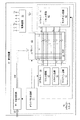
図4は、本発明の実施形態による、PDP10用のサステイン回路63および67に用いられるパルス電圧印加回路602を示している。 FIG. 4 shows a pulse
図4において、PDP10のn対の表示電極XおよびYは複数のg個のグループG1、G2、...Gg(2≦g≦n)に分割されている。個数gは、好ましくは例えばg=8〜10であるが、それより少なくてもまたは多くてもよい。グループG1、G2、...Ggにおけるそれぞれの表示電極対の数は、概ね互いに等しいが、正確に互いに等しくなくてもよい。ここでは、簡単化のために各グループG1〜Ggの表示電極対の数は等しいものとする。従って、各グループのn/g対の表示電極XおよびYは、合計容量Cpb=nC/gを有し、例えばg=8に対して25nFのオーダの合計容量Cpbを有する。 In FIG. 4, the n pairs of display electrodes X and Y of the
パルス電圧印加回路602は、電気的エネルギ回収すなわち電力回収機能を有するパルス電力供給および回収回路110と、それぞれのグループG1〜Ggにそれぞれ設けられたクランプ回路141、142、・・・148と、制御信号発生回路160と、を具えている。 The pulse
パルス電力供給および回収回路110は、パルスPsの立ち上がりにおいてそれぞれのグループG1〜Ggのn/g対の電極XおよびYに電力を供給しパルスPsの立ち下がりにおいて電力を回収する。クランプ回路141〜148の各々は、対応するグループの互いに並列に接続されたn/g対の表示電極XおよびYの間の電圧VCpbを所定の電圧Vsにクランプする。The pulse power supply and
パルス電力供給および回収回路110は、一端子が共通導体電位または接地点GNDに結合された電力回収キャパシタCrと、回収キャパシタCrに直列に接続されかつ経路1を形成するように回収キャパシタCrの他端子にスイッチSW1を介してアノード(陽極)が結合されたダイオードD1と、キャパシタCrに直列に接続されかつダイオードD1と並列に経路2を形成するように回収キャパシタCrの他端子にスイッチSW2を介してカソード(陰極)が結合されたダイオードD2と、ダイオードD1のカソードとダイオードD2のアノードの接続点にそれぞれの一方の端子が結合されかつそれぞれのグループG1〜Ggのn/g対の表示電極XおよびYのうちの一方の表示電極(XまたはY)に他方の端子が結合された共通の共振インダクタL21〜L28と、を含んでいる。 The pulse power supply and
それぞれのグループG1〜Ggのn/g対の電極XおよびYに対して、共通の共振インダクタL21〜L28がそれぞれ設けられている。共振インダクタL21〜L28は互いに等しいインダクタンスL2を有する。インダクタンスL2は、図3のインダクタL1のインダクタンスLのg倍より幾分小さい値g’L(g’<g)に設定され、例えば400nH〜5mHの値である。例えば、gが8の場合、g’の値は7であればよい。Common resonant inductors L21 to L28 are provided for the n / g pairs of electrodes X and Y of the groups G1 to Gg, respectively. Resonant inductor L21~L28 have equal inductance L 2 each other. Inductance L 2 is set to a somewhat smaller value g'L (g '<g) than g times the inductance L of the inductor L1 of FIG. 3, for example, a value of 400NH~5mH. For example, when g is 8, the value of g ′ may be 7.
電力クランプ回路141〜148の各々は、対応するグループG1、G2、...またはGgの表示電極対XおよびYの一方の表示電極XまたはYの接続点に対応するスイッチSW21、SW22、...SW28を介して結合される所定の電圧Vsの定電圧源Vsと、その接続点に対応するスイッチSW41、SW42、...SW48を介して結合される共通導体電位または接地点GNDと、を含んでいる。クランプ回路141、142、・・・148は、互いに同様の構成を有する。 Each of the power clamp circuits 141-148 has a corresponding group G1, G2,. . . Or switches SW21, SW22,... Corresponding to the connection point of one display electrode X or Y of the display electrode pair X and Y of Gg. . . A constant voltage source Vs of a predetermined voltage Vs coupled through SW28 and switches SW41, SW42,. . . And a common conductor potential or ground point GND coupled via SW48. The
制御信号発生回路160は、パルス電力供給および回収回路110およびクランプ回路141〜148におけるスイッチSW1、SW21、・・・SW28、SW3、SW41、・・・SW48のオン/オフ動作を制御する信号CSW1、CSW21、・・・CSW 28、CSW3、CSW41、・・・CSW48を発生する。スイッチSW1、SW21〜SW28、SW3、およびSW41〜SW48は、トランジスタであってもよい。The control
図5は、本発明の実施形態による、スイッチSW1〜SW48を制御するための図4の制御信号発生回路160の制御信号CSW1〜CSW48のオン/オフの状態と、パルス印加時の表示電極キャパシタCpbおよび回収キャパシタCrの両端間の電圧VCpbおよびVCrの概略の波形を示している。FIG. 5 shows the on / off states of the control signals C SW1 to C SW48 of the control
図4および5を参照すると、パルス電圧印加回路602において、図1の表示装置60の電源を投入して回収キャパシタが充放電を繰り返した後の定常動作状態において、回収キャパシタCrにほぼ電圧Vs/2の電荷が蓄積されており、各グループの表示電極容量Cpbには電荷が蓄積されていないものとする。従って、各グループ表示電極容量Cpbすなわち各キャパシタンスCにおける電圧VCpbの値はゼロ(0)である。4 and 5, in the pulse
パルスPsの立ち上がりの開始のタイミングt1において、制御信号CSW1に従ってスイッチSW1がターンオンすると、経路1が形成されて、回収キャパシタCrからスイッチSW1、ダイオードD1および共振インダクタL21〜L28の各々を介して各グループ表示電極容量Cpbに供給電流が流れ、電荷q〜CpbVsが各グループ表示電極容量Cpbに蓄積され、各グループ表示電極容量Cpbの電圧VCpbが上昇し、パルスPsの立ち上がりが形成される。各グループ表示電極容量Cpbの電圧VCpbがピーク電圧Vpmaxに達したとき、制御信号CSW21〜CSW28に従ってタイミングt2においてクランプ回路141〜148のスイッチSW21〜SW28がターンオンされる。なお、ダイオードD1によってその供給電流とは逆方向に電流は流れない。従って、スイッチSW1は、そのピーク電圧への到達後からスイッチSW21〜SW28のターンオフのタイミングまでの間の任意のタイミングでターンオフしてよい。そのピーク電圧Vpmaxは電圧Vsより僅かに低い。この場合、立ち上がり時間Trは、図3の従来技術のパルス電力供給および回収回路11の場合より短くなる。クランプ回路141〜148の電圧源Vsは、各グループ表示電極容量Cpbの電圧VCpbを電圧Vsにクランプし、各グループ表示電極容量Cpbの電圧VCpbを電圧Vsに維持する。クランプ回路141〜148はパネル容量Cpbの電圧VCpbを所定の電圧Vsになるように補償する。その後、サステイン放電が生じ、制御信号CSW21〜CSW28に従ってSW21〜SW28がターンオフされる。In the timing t1 of the start of the rise of the pulse Ps, the switch SW1 is turned on according to the control signal C SW1, path 1 is formed, each from the recovery capacitor Cr via the respective switches SW1, diode D1 and the resonant inductor L21~L28 group display electrode capacitance Cpb supply current flows, the charge q~CpbVs are accumulated in each group display electrode capacitance Cpb, the voltage V Cpb rises of each group display electrode capacitance Cpb, the rise of the pulse Ps is formed. When the voltage V Cpb of each group display electrode capacitance Cpb peaked voltage Vpmax, switch SW21~SW28 clamp circuit 141-148 is turned in the timing t2 in accordance with the control signal C SW21 -C SW28. Note that no current flows in the direction opposite to the supply current by the diode D1. Therefore, the switch SW1 may be turned off at an arbitrary timing after reaching the peak voltage until the turn-off timing of the switches SW21 to SW28. The peak voltage Vpmax is slightly lower than the voltage Vs. In this case, the rise time Tr is shorter than in the case of the conventional pulse power supply and
パルスPsの立ち下がりの開始のタイミングt3において、制御信号CSW3に従ってスイッチSW3がターンオンされると、各グループ表示電極容量Cpbから共振インダクタL21〜L28、ダイオードD2およびスイッチSW3を介して回収キャパシタCrに還流電流が流れ、電荷q〜gCpbVsが回収キャパシタCrに蓄積され、各グループ表示電極容量Cpbの電圧が下降し、パルスPsの立ち下がりが形成される。各グループ表示電極容量Cpbの電圧VCpbがほぼ負方向のピーク電圧Vpminに達したとき、タイミングt4において制御信号CSW41〜CSW48に従ってスイッチSW41〜SW48がターンオンされる。なお、ダイオードD2によってその還流電流とは逆方向に電流は流れない。従って、スイッチSW3は、そのピーク電圧への到達後からスイッチSW41〜SW48のターンオフのタイミングまでの間の任意のタイミングでターンオフしてよい。そのピーク電圧Vpminは接地電位GNDまたは0Vより僅かに高い。この場合、立ち下がり時間Trは、図3の従来技術のパルス電力供給および回収回路11の場合より短くなる。クランプ回路141〜148の接地点GNDは、各グループ表示電極容量Cpbの電圧VCpbを接地電位GNDまたは0Vにクランプする。その後、次のタイミングt1の前に、制御信号CSW41〜CSW48に従ってスイッチSW41〜SW48がターンオフされる。その後、同様の動作が繰り返される。In the timing t3 of the start of the fall of the pulse Ps, the switch SW3 is turned on according to the control signal C SW3, resonant inductor L21~L28 from each group display electrode capacitance Cpb, the recovery capacitor Cr through diode D2 and the switch SW3 A reflux current flows, charges q to gCpbVs are accumulated in the recovery capacitor Cr, the voltage of each group display electrode capacitor Cpb is lowered, and the falling of the pulse Ps is formed. When the voltage V Cpb of each group display electrode capacitance Cpb reaches approximately negative peak voltage Vpmin, switch SW41~SW48 is turned in accordance with the control signal C SW41 -C SW48 at the timing t4. Note that no current flows in the direction opposite to the return current by the diode D2. Therefore, the switch SW3 may be turned off at an arbitrary timing after reaching the peak voltage until the turn-off timing of the switches SW41 to SW48. The peak voltage Vpmin is slightly higher than the ground potential GND or 0V. In this case, the fall time Tr is shorter than that of the conventional pulse power supply and
図6Aおよび6Bは、図3のパルス電力供給および回収回路11と図4のパルス電力供給および回収回路110によるパルスPsの波形の比較を示している。この場合、パルス電力供給および回収回路110において、インダクタL21〜L28の値L2をgLよりできるだけ小さくした(L2=g’L<gL)ものである。パルスPsの立ち上がり時間および立ち下がり時間Trが、図3のパルス電力供給および回収回路11のパルスPsより短くなっている。 6A and 6B show a comparison of the waveform of the pulse Ps by the pulse power supply and
図7Aおよび7Bは、図3のパルス電力供給および回収回路11と図4のパルス電力供給および回収回路110による別のパルスPsの波形の比較を示している。この場合、パルス電力供給および回収回路110において、インダクタL21〜L28の値L2をgLにした(L2=gL)ものである。パルスPsの立ち上がり時間および立ち下がり時間Trは図3のパルス電力供給および回収回路11のパルスPsと同じであるが、図3のパルス電力供給および回収回路11のパルスPsより、ピーク電圧Vpmaxが高く、ピーク電圧Vpminが低く、電力供給効率および電力回収効率ηはより高くなる。 7A and 7B show a comparison of the waveforms of another pulse Ps by the pulse power supply and
図8は、図4のパルス電圧印加回路602を変形した本発明の別の実施形態によるパルス電圧印加回路604を示している。パルス電圧印加回路604では、ダイオードD1のカソードに結合されるインダクタL21〜L28は図4のものと同じであるが、ダイオードD2のアノードに結合されるインダクタL31、L32、...L38の各々のインダクタンスL3は、インダクタL21〜L28のインダクタンスL2より大きい(L3>L 2)。この場合、パルスPsの立ち上がり時間Trが短くし、パルスPsの立ち下がりにおける負方向のピークVpminをより低くして電力回収効率ηが高くすることができる。 FIG. 8 shows a pulse
代替構成として、図4および8におけるスイッチSW1とダイオードD1の配置は入れ替えてもよい。同様に、スイッチSW3とダイオードD2の配置は入れ替えてもよい。 As an alternative configuration, the arrangement of switch SW1 and diode D1 in FIGS. 4 and 8 may be interchanged. Similarly, the arrangement of the switch SW3 and the diode D2 may be switched.
図9は、本発明の別の実施形態による、PDP10用のサステイン回路63および67に用いられる、図4のパルス電圧印加回路602と、これと同じ構成の別のパルス電圧印加回路603とを示している。この場合、n対の表示電極XおよびYは複数の2g個のグループG1、G2...G2g(2≦g≦n/4)に分割されている。第1のg個のグループG1〜Ggの表示電極対XおよびYに対してパルス電圧印加回路602が設けられ、第2のg個のグループGg+1〜G2gの表示電極対XおよびYに対してパルス電圧印加回路603が設けられている。同様に、n対の表示電極XおよびYを3g個以上のグループに分割して、パルス電圧印加回路602と同じ構成の3個以上のパルス電圧印加回路を設け、その際、各g個のグループに対して1つのパルス電圧印加回路を対応付けてもよい。 FIG. 9 shows the pulse
同様に、n対の表示電極XおよびYを2g個以上のグループに分割して、図8のパルス電圧印加回路604同じ構成の2つ以上のパルス電圧印加回路を設け、その際、各g個のグループに対して1つのパルス電圧印加回路を対応付けてもよい。 Similarly, the n pairs of display electrodes X and Y are divided into 2g or more groups, and two or more pulse voltage application circuits having the same configuration as those of the pulse
以上、PDPについて説明したが、本発明は、これに限定されることなく、例えば、有機および無機EL、および電圧の印加により電荷を蓄積することで文字などを表示させる電子ペーパーにも適用可能である。 Although the PDP has been described above, the present invention is not limited to this, and can be applied to, for example, organic and inorganic EL, and electronic paper that displays characters by storing charges by applying voltage. is there.
以上説明した実施形態は典型例として挙げたに過ぎず、その各実施形態の構成要素を組み合わせること、その変形およびバリエーションは当業者にとって明らかであり、当業者であれば本発明の原理および請求の範囲に記載した発明の範囲を逸脱することなく上述の実施形態の種々の変形を行えることは明らかである。 The embodiments described above are merely given as typical examples, and it is obvious to those skilled in the art to combine the components of each embodiment, and variations and variations thereof will be apparent to those skilled in the art. Obviously, various modifications may be made to the above-described embodiments without departing from the scope of the invention as set forth in the scope.
Claims (7)
前記複数のキャパシタンスは複数g個のグループに分けられ、
共通導体電位に一端子が結合された電気的エネルギ回収用の回収用キャパシタと、
前記g個のグループにそれぞれ対応付けられた複数の共振インダクタと、を具え、
前記複数の共振インダクタのそれぞれの一方の端子は前記g個のそれぞれのグループのキャパシタンスに結合され、前記複数の共振インダクタのそれぞれの他方の端子は前記回収用キャパシタの他端子に第1のスイッチおよび第2のスイッチを介して結合され、
さらに、前記第1のスイッチをオンすることにより前記回収用キャパシタからg個の前記共振インダクタを介して前記g個のそれぞれのグループのキャパシタンスを充電する第1の経路形成手段と、
前記第2のスイッチをオンすることにより前記g個のグループのキャパシタンスを放電させて、g個の前記共振インダクタをそれぞれ介して前記回収用キャパシタに電気的エネルギを回収する第2の経路形成手段と、
前記第1と第2の経路形成手段を制御する制御手段と、を具え、
前記g個のグループの中の各グループの電極は、それぞれ、第3のスイッチを介して第1の電圧源に接続され、第4のスイッチを介して前記共通導体電位に接続され、
前記制御手段は、前記g個のグループのキャパシタンスに対して共通に設けられた前記第1のスイッチと前記第2のスイッチを制御し、かつ、前記第3のスイッチと第4のスイッチを前記g個のグループに対してそれぞれ同じタイミングで制御することを特徴とする充放電装置。A charging / discharging device that charges and discharges a plurality of capacitances by applying a voltage,
The plurality of capacitances are divided into a plurality of g groups;
A recovery capacitor for electrical energy recovery in which one terminal is coupled to a common conductor potential;
A plurality of resonant inductors respectively associated with the g groups,
One terminal of each of the plurality of resonant inductors is coupled to the capacitance of each of the g groups, and the other terminal of each of the plurality of resonant inductors is connected to the other terminal of the recovery capacitor with a first switch and Coupled through a second switch ,
A first path forming means for charging the capacitance of each of the g groups from the recovery capacitor via the g resonant inductors by turning on the first switch ;
A second path forming means for discharging the g groups of capacitances by turning on the second switch and recovering electrical energy to the recovery capacitors via the g resonant inductors; ,
Control means for controlling the first and second path forming means,
The electrodes of each group in the g groups are connected to the first voltage source via a third switch, and connected to the common conductor potential via a fourth switch, respectively.
The control means controls the first switch and the second switch provided in common for the capacitances of the g groups, and controls the third switch and the fourth switch to the g A charge / discharge device that controls each group at the same timing .
前記セルに対応して複数の電極が設けられており、
前記複数の電極は複数g個のグループに分けられ、
前記回収用キャパシタは一端子が共通導体電位に結合され、
前記g個のグループに複数の共振インダクタがそれぞれ対応付けられ、
前記複数の共振インダクタのそれぞれの一方の端子は前記g個のそれぞれのグループの電極に結合され、前記複数の共振インダクタのそれぞれの他方の端子は前記回収用キャパシタの他端子に第1のスイッチおよび第2のスイッチを介して結合され、
前記第1のスイッチをオンすることにより前記回収用キャパシタからg個の前記共振インダクタを介して前記g個のそれぞれのグループの電極に対応するセルに電気的エネルギを供給する第1の経路形成手段と、
前記第2のスイッチをオンすることにより前記g個のグループの電極に対応するセルのキャパシタンスを放電させて、g個の前記共振インダクタをそれぞれ介して前記回収用キャパシタに電気的エネルギを回収する第2の経路形成手段と、
前記第1と第2の経路形成手段を制御する制御手段と、を具え、
前記g個のグループの中の各グループの電極は、それぞれ、第3のスイッチを介して第1の電圧源に接続され、第4のスイッチを介して前記共通導体電位に接続され、
前記制御手段は、前記g個のグループのキャパシタンスに対して共通に設けられた前記第1のスイッチと前記第2のスイッチを制御し、かつ、前記第3のスイッチと第4のスイッチを前記g個のグループに対してそれぞれ同じタイミングで制御することを特徴とするプラズマ・ディスプレイ・パネル。A plasma display panel that performs charging to transfer electrical energy from a recovery capacitor for recovering electrical energy to a cell constituting a screen and power recovery to transfer electrical energy from the cell to the recovery capacitor. There,
A plurality of electrodes are provided corresponding to the cells,
The plurality of electrodes are divided into a plurality of g groups,
The recovery capacitor has one terminal coupled to a common conductor potential,
A plurality of resonant inductors are respectively associated with the g groups,
One terminal of each of the plurality of resonant inductors is coupled to the respective electrodes of the g groups, and the other terminal of each of the plurality of resonant inductors is connected to the other terminal of the recovery capacitor with a first switch and Coupled through a second switch ,
By turning on the first switch, first path forming means for supplying electrical energy from the recovery capacitor to the cells corresponding to the respective electrodes of the g groups via the g resonant inductors. When,
By turning on the second switch, the capacitance of the cells corresponding to the g groups of electrodes is discharged, and electrical energy is recovered in the recovery capacitor via the g resonant inductors. Two path forming means;
Control means for controlling the first and second path forming means ,
The electrodes of each group in the g groups are connected to the first voltage source via a third switch, and connected to the common conductor potential via a fourth switch, respectively.
The control means controls the first switch and the second switch provided in common for the capacitances of the g groups, and controls the third switch and the fourth switch to the g A plasma display panel , wherein each group is controlled at the same timing .
前記セルに対応して複数の電極が設けられており、
前記複数の電極は複数g個のグループに分けられ、
前記回収用キャパシタは一端子が共通導体電位に結合され、
前記g個のグループに複数の共振インダクタがそれぞれ対応付けられ、
前記複数の共振インダクタのそれぞれの一方の端子は前記g個のそれぞれのグループのキャパシタンスに結合され、前記複数の共振インダクタのそれぞれの他方の端子は前記回収用キャパシタの他端子に第1のスイッチおよび第2のスイッチを介して結合され、
第1の経路形成手段と、第2の経路形成手段と、
前記第1と第2の経路形成手段を制御する制御手段と、を具え、
前記g個のグループの中の各グループの電極は、それぞれ、第3のスイッチを介して第1の電圧源に接続され、第4のスイッチを介して前記共通導体電位に接続され、
前記制御手段は、前記g個のグループのキャパシタンスに対して共通に設けられた前記第1のスイッチと前記第2のスイッチを制御し、かつ、前記第3のスイッチと第4のスイッチを前記g個のグループに対してそれぞれ同じタイミングで制御し、
前記第1の経路形成手段が、前記セルに印加されるパルスの立ち上がり期間において、前記第1のスイッチをオンすることにより、前記回収用キャパシタの他端子から、g個の前記共振インダクタを介して前記g個のそれぞれのグループの電極のキャパシタンスを充電し、
前記第2の経路形成手段が、前記パルスの立ち下がり期間において、前記第2のスイッチをオンすることにより、g個の前記共振インダクタを介して前記g個のそれぞれのグループの電極のキャパシタンスを放電させて、前記回収用キャパシタに電気的エネルギを回収することを特徴とする、充放電の方法。A charge / discharge method for charging / discharging cells constituting a screen of a plasma display panel,
A plurality of electrodes are provided corresponding to the cells,
The plurality of electrodes are divided into a plurality of g groups,
The recovery capacitor has one terminal coupled to a common conductor potential,
A plurality of resonant inductors are respectively associated with the g groups,
One terminal of each of the plurality of resonant inductors is coupled to the capacitance of each of the g groups, and the other terminal of each of the plurality of resonant inductors is connected to the other terminal of the recovery capacitor with a first switch and Coupled through a second switch,
A first path forming means, a second path forming means,
Control means for controlling the first and second path forming means,
The electrodes of each group in the g groups are connected to the first voltage source via a third switch, and connected to the common conductor potential via a fourth switch, respectively.
The control means controls the first switch and the second switch provided in common for the capacitances of the g groups, and controls the third switch and the fourth switch to the g Control each group at the same time,
The first path forming means turns on the first switch during a rising period of a pulse applied to the cell, thereby allowing g from the other terminals of the recovery capacitor to pass through the g resonance inductors. Charging the capacitance of each of the g groups of electrodes;
The second path forming means turns on the second switch during the falling period of the pulse, thereby discharging the capacitances of the respective electrodes of the g groups through the g resonant inductors. And charging and discharging the electrical energy to the recovery capacitor.
Applications Claiming Priority (1)
| Application Number | Priority Date | Filing Date | Title |
|---|---|---|---|
| PCT/JP2005/002900 WO2006090444A1 (en) | 2005-02-23 | 2005-02-23 | Charging/discharging apparatus, display apparatus, plasma display panel, and charging/discharging method |
Publications (2)
| Publication Number | Publication Date |
|---|---|
| JPWO2006090444A1 JPWO2006090444A1 (en) | 2008-07-17 |
| JP4372191B2 true JP4372191B2 (en) | 2009-11-25 |
Family
ID=36927095
Family Applications (1)
| Application Number | Title | Priority Date | Filing Date |
|---|---|---|---|
| JP2007504579A Expired - Fee Related JP4372191B2 (en) | 2005-02-23 | 2005-02-23 | Charging / discharging device, display device, plasma display panel, and charging / discharging method |
Country Status (2)
| Country | Link |
|---|---|
| JP (1) | JP4372191B2 (en) |
| WO (1) | WO2006090444A1 (en) |
Family Cites Families (7)
| Publication number | Priority date | Publication date | Assignee | Title |
|---|---|---|---|---|
| JP2705948B2 (en) * | 1988-09-01 | 1998-01-28 | 株式会社日立製作所 | Matrix type panel display |
| JP2746792B2 (en) * | 1992-03-19 | 1998-05-06 | 富士通株式会社 | AC Drive Type Plasma Display Panel Driver and Control Method Thereof |
| JP3241577B2 (en) * | 1995-11-24 | 2001-12-25 | 日本電気株式会社 | Display panel drive circuit |
| JP3672669B2 (en) * | 1996-05-31 | 2005-07-20 | 富士通株式会社 | Driving device for flat display device |
| JP3036496B2 (en) * | 1997-11-28 | 2000-04-24 | 日本電気株式会社 | Driving method and circuit for plasma display panel and plasma display panel display |
| JPH11231829A (en) * | 1998-02-18 | 1999-08-27 | Fujitsu Ltd | Driving method and drive device for plasma display panel |
| JPH11338418A (en) * | 1998-05-26 | 1999-12-10 | Mitsubishi Electric Corp | Driving method of plasma display panel and plasma display device |
-
2005
- 2005-02-23 WO PCT/JP2005/002900 patent/WO2006090444A1/en not_active Application Discontinuation
- 2005-02-23 JP JP2007504579A patent/JP4372191B2/en not_active Expired - Fee Related
Also Published As
| Publication number | Publication date |
|---|---|
| JPWO2006090444A1 (en) | 2008-07-17 |
| WO2006090444A1 (en) | 2006-08-31 |
Similar Documents
| Publication | Publication Date | Title |
|---|---|---|
| EP1291836B1 (en) | Apparatus for and method of driving a plasma display panel | |
| US7193586B2 (en) | Apparatus and methods for driving a plasma display panel | |
| US7492333B2 (en) | Plasma display device and driving method thereof | |
| US7586486B2 (en) | Display panel driving apparatus | |
| US7170474B2 (en) | Plasma display panel driver, driving method thereof, and plasma display device | |
| JP4338766B2 (en) | Plasma display panel drive circuit | |
| JP4324629B2 (en) | Charge / discharge device, plasma display panel, and charge / discharge method | |
| US7221334B2 (en) | Energy recovery circuit of plasma display panel and driving apparatus of plasma display panel including energy recovery circuit | |
| US20070040767A1 (en) | Plasma display apparatus | |
| KR100740089B1 (en) | Plasma display device and driving method thereof | |
| JP4357564B2 (en) | Charging / discharging device, display device, plasma display panel, and charging / discharging method | |
| JP4372191B2 (en) | Charging / discharging device, display device, plasma display panel, and charging / discharging method | |
| JP2000181405A (en) | Driving method of display panel and display device | |
| KR100670183B1 (en) | Plasma display device and driving method thereof | |
| US7652641B2 (en) | Driving apparatus of plasma display panel | |
| JP2003233343A (en) | Display panel driving circuit | |
| JPWO2006100722A1 (en) | Charging / discharging device, display device, plasma display panel, and charging / discharging method | |
| KR100870689B1 (en) | Charging/discharging device, plasma display panel, and charging/discharging method | |
| US8111213B2 (en) | Plasma display device and driving method thereof | |
| EP1708161A2 (en) | Plasma display apparatus and driving method thereof | |
| KR100649193B1 (en) | Plasma display device and driving method thereof | |
| US20100026672A1 (en) | Circuit for driving a plasma display panel | |
| US20080111495A1 (en) | Energy recovery circuit of display panel and apparatus for driving display panel including the same | |
| JP2005182074A (en) | Driving device for display panel |
Legal Events
| Date | Code | Title | Description |
|---|---|---|---|
| A131 | Notification of reasons for refusal |
Free format text: JAPANESE INTERMEDIATE CODE: A131 Effective date: 20090127 |
|
| A521 | Request for written amendment filed |
Free format text: JAPANESE INTERMEDIATE CODE: A523 Effective date: 20090327 |
|
| A131 | Notification of reasons for refusal |
Free format text: JAPANESE INTERMEDIATE CODE: A131 Effective date: 20090602 |
|
| A521 | Request for written amendment filed |
Free format text: JAPANESE INTERMEDIATE CODE: A523 Effective date: 20090724 |
|
| TRDD | Decision of grant or rejection written | ||
| A01 | Written decision to grant a patent or to grant a registration (utility model) |
Free format text: JAPANESE INTERMEDIATE CODE: A01 Effective date: 20090825 |
|
| A01 | Written decision to grant a patent or to grant a registration (utility model) |
Free format text: JAPANESE INTERMEDIATE CODE: A01 |
|
| A61 | First payment of annual fees (during grant procedure) |
Free format text: JAPANESE INTERMEDIATE CODE: A61 Effective date: 20090901 |
|
| FPAY | Renewal fee payment (event date is renewal date of database) |
Free format text: PAYMENT UNTIL: 20120911 Year of fee payment: 3 |
|
| R150 | Certificate of patent or registration of utility model |
Free format text: JAPANESE INTERMEDIATE CODE: R150 |
|
| LAPS | Cancellation because of no payment of annual fees |