JP4370751B2 - Nitride semiconductor laser device and manufacturing method thereof - Google Patents
Nitride semiconductor laser device and manufacturing method thereof Download PDFInfo
- Publication number
- JP4370751B2 JP4370751B2 JP2002040228A JP2002040228A JP4370751B2 JP 4370751 B2 JP4370751 B2 JP 4370751B2 JP 2002040228 A JP2002040228 A JP 2002040228A JP 2002040228 A JP2002040228 A JP 2002040228A JP 4370751 B2 JP4370751 B2 JP 4370751B2
- Authority
- JP
- Japan
- Prior art keywords
- nitride semiconductor
- layer
- reflecting mirror
- laser device
- semiconductor laser
- Prior art date
- Legal status (The legal status is an assumption and is not a legal conclusion. Google has not performed a legal analysis and makes no representation as to the accuracy of the status listed.)
- Expired - Fee Related
Links
Images


Description
【0001】
【発明の属する技術分野】
本発明は窒化物半導体(InXAlYGa1-X-YN、0≦X、0≦Y、X+Y≦1)よりなるレーザ素子に関する。
【0002】
【従来の技術】
窒化物半導体は高輝度青色LED、純緑色LEDの材料として、フルカラーLEDディスプレイ、交通信号灯等で最近実用化されたばかりである。また、本出願人は、最近この材料を用いてパルス電流において、室温での410nmのレーザ発振を発表した(例えば、文献A:Jpn.J.Appl.Phys. Vol.35 (1996) pp.L217-L220、文献B:Appl.Phys.Lett.69(10),2 Sep.1996 pp.1477-1479等)
【0003】
窒化物半導体よりなるレーザ素子の共振面は一般にエッチング、劈開等の技術を用いて形成される。前記文献Aでは、窒化物半導体をエッチングして対向する共振面を形成しており、またBでは、サファイアA面上に窒化物半導体を成長させ、そのサファイアのR面で劈開することにより共振面を形成している。しかし、それらのレーザ素子の出力は未だ低く満足できるものではなかった。
【0004】
【発明が解決しようとする課題】
従って、本発明はこのような事情を鑑みて成されたものであって、その主たる目的は、出力の向上した窒化物半導体よりなるレーザ素子と、その製造方法を提供することにある。
【0005】
【課題を解決するための手段】
本発明に係る窒化物半導体レーザ素子は、基板上に、それぞれ窒化物半導体からなるn型層、活性層、p型層が積層されたダブルヘテロ構造を有し、その窒化物半導体層の対向する端面を共振面とする窒化物半導体レーザ素子において、
前記共振面の一方はエッチング面であり、他方は窒化物半導体の劈開面であり、
前記p型層にはストライプ状のリッジが形成され、該リッジの最上部にp電極が形成され、
誘電体からなる反射鏡が、前記エッチング面を含む基板上にある窒化物半導体層の表面に連続して形成され、
前記p電極と接続するpパッド電極が前記反射鏡を介してp型層の表面にも渡って形成されたことを特徴とする。
【0006】
前記劈開面には、第2の反射鏡が形成されていてもよい。
【0007】
前記反射鏡は、SiO 2 、TiO 2 、ZrO 2 、ポリイミドのいずれか1つ以上で形成されていてもよい。
【0008】
前記エッチング共振面には、共振面とほぼ垂直な位置にあるn層の平面が露出していてもよい。
【0009】
前記他方の共振面は窒化物半導体がM面
【外1】

【0010】
前記劈開面にはレーザ光を窒化物半導体層内に反射させる反射鏡が形成されており、前記エッチング面に形成された反射鏡の反射率が、劈開面に形成された反射鏡の反射率よりも高く調整されていることが好ましい。
【0011】
本発明に係る窒化物半導体レーザ素子の製造方法は、
基板上に、それぞれ窒化物半導体からなるn型層、活性層、p型層を積層する工程と、
前記p型層をエッチングしてストライプ状のリッジを形成する工程と、
前記p型層及び活性層をエッチングして、それぞれ共振面となる対向するエッチング端面を形成し、n型層を露出させる工程と、
前記リッジの最上部にp電極を形成する工程と、
前記p電極上を含む、前記基板から上に露出している層全てに渡って誘電体膜よりなる反射鏡を形成する工程と、
前記p電極上の反射鏡を除去する工程と、
前記p電極に接続するpパッド電極を、前記反射鏡を介してp型層の表面に渡って形成する工程と、
前記互いに対向する共振面の間において窒化物半導体を劈開する工程とを備えることを特徴とする。
【0012】
窒化物半導体を劈開した後、前記エッチング面に形成された反射鏡よりも活性層の発光波長の反射率が低い他の反射鏡を、前記劈開面に形成することを含んでいてもよい。
【0013】
前記窒化物半導体を劈開する工程の後に、窒化物半導体の劈開面に第2の反射鏡を設ける工程を備えていてもよい。
【0015】
【発明の実施の形態】
図1は本発明のレーザ素子の形状を示す斜視図であり、図2は図1のレーザ素子を、一点鎖線で示す位置で共振方向に平行に切断した際の概略的な断面図である。基本構造としては、基板上に、窒化物半導体よりなるn型層、活性層、p型層が積層されたダブルへテロ構造を有し、それらの窒化物半導体層の端面には互いに対向する共振面を有している。それら共振面は活性層の発光波長において異なる反射率を有している。具体的な共振面としては、一方が窒化物半導体のエッチング面とされており、もう一方が窒化物半導体の劈開面とされている。
【0016】
窒化物半導体をエッチングするには、ウエットエッチング、ドライエッチング等の方法があるが、共振面となるような平滑な面を形成するには、好ましくドライエッチングを用いる。ドライエッチングには、例えば反応性イオンエッチング(RIE)、反応性イオンビームエッチング(RIBE)、電子サイクロトロンエッチング(ECR)、イオンビームエッチング等の装置があり、いずれもエッチングガスを適宜選択することにより、窒化物半導体をエッチングして共振面を形成することができる。例えば、本出願人が先に公開した特開平8−17803号公報に、窒化物半導体の具体的なエッチング手段が開示されている。
【0017】
一方、劈開により窒化物半導体の端面に共振面を形成するには、例えば、本出願人が先に公開した特開平8−153931号に記載されているような、サファイアのC面にC軸配向した窒化物半導体を成長させた後、サファイア基板をM面で割る方法がある。その他、上記文献Bに記載されるような、サファイアA面上に窒化物半導体を成長させ、そのサファイアのR面で劈開する方法等がある。本発明のレーザ素子において、窒化物半導体の劈開面の面方位は特に問わないが、好ましくは窒化物半導体のM面を共振面とすると、非常に歩留良く、また鏡面に近い共振面が得られる。なお本発明でいう共振面とは、図1の矢印で示すように、活性層の端面に形成する共振面を指す。
【0018】
このように窒化物半導体の一方の共振面をエッチング面とし、さらにもう一方の共振面をエッチング面とすることにより、レーザ素子の共振面の反射率を異なるようにすることができるので、反射率の低い共振面より出射されるレーザ光の出力を向上させることができる。特に、図1、2に示すようにエッチング面側の共振面に活性層の発光波長を反射する第1の反射鏡を形成すると、劈開面側の反射率がさらに小さくなるので、劈開面よりレーザ光が直接出射されるため出力の高いレーザ素子が得られる。
【0019】
さらにまた、エッチングにより共振面を形成すると、図1に示すようにエッチング共振面側には、共振面とほぼ垂直な位置にあるn層の平面が露出してしまう。この平面はレーザ光をその表面で反射して、レーザ光のファーフィールドパターンを乱す。つまりレーザ出射光側に共振面よりも突出した平面が存在すると、その平面でレーザ光の形状が乱される。一方劈開面であれば、その突出部分がないために、楕円形に近い一定形状のレーザ光が得られる。そのため、本発明のレーザ素子では劈開面側から出射されるレーザ光を主として取り出して、各種光源として使用することが望ましい。
【0020】
さらに好ましくは、図1に示すようにエッチング面側には第1の反射鏡を形成して、劈開面側には反射鏡を形成しないことが最も望ましい。レーザ光は共振面より出射される場合に反射鏡で一部が出射を阻害される。そのため、劈開面側に反射鏡を形成しないことにより、光の取出効率が向上し、スロープ効率もよくなるので、高出力のレーザが得られる。さらに好ましくは反射鏡がSiO2、TiO2、ZrO2、ポリイミドのような高誘電体で構成されていると、本発明の製造方法においても非常に都合がよい。つまり、窒化物半導体レーザ素子の場合には、同一面側にある半導体層からp電極と、n電極とが取り出されることが多いため、電極形成の際に、電極間の短絡には非常に注意を要する。しかし、本発明のように高誘電体よりなる反射鏡を共振面と共に形成すると、その反射鏡がn、p電極が短絡するのを防止する絶縁膜として作用するので、レーザ素子の信頼性が向上する。この誘電体よりなる反射鏡の作用については、本実施例においてさらに詳説する。
【0021】
本発明のレーザ素子では、エッチング面側に形成した第1の反射鏡の反射率よりも低い反射率を有する第2の反射鏡を劈開面側に形成してもよい。第2の反射鏡を形成すると、閾値が低下するという利点はあるが、劈開面側から出射されるレーザ素子の出力は、第2の反射鏡を形成しないものに比較して、若干低下する。
【0022】
【実施例】
次に、本発明を実施例において詳説する。図3は本発明のレーザ素子の一構造を示す模式的な断面図であり、共振面に平行な方向で素子を切断した際の構造を示している。図4は窒化物半導体の結晶構造を示すブロックセル図である。図5、図6は本発明の実施例の一工程において得られるレーザ素子の構造を示す部分断面図であり、この図はレーザ光の共振方向に平行な方向で素子を切断した際の図を示している。以下、これらの図を元に本発明のレーザ素子、及び製造方法について説明する。
【0023】
[実施例1]
以下、図3に示す構造のレーザ素子を作製する方法について述べる。
(積層工程)
1) 2インチφのサファイア(C面)よりなる基板1の上に
2) GaNよりなるバッファ層2
3) Siドープn型GaNよりなるコンタクト層3
4) Siドープn型In0.1Ga0.9Nよりなるクラック防止層4
5) Siドープn型Al0.2Ga0.8Nよりなるn型クラッド層5
6) SiドープGaNよりなるn型光ガイド層6
7) SiドープIn0.2Ga0.8Nよりなる井戸層を25オングストロームと、SiドープIn0.01Ga0.95Nよりなる障壁層を50オングストロームと3ペア積層して最後に井戸層を積層した活性層7
8) Mgドープp型Al0.1Ga0.9Nよりなるp型キャップ層8
9) Mgドープp型GaNよりなるp型光ガイド層9
10) Mgドープp型Al0.2Ga0.8Nよりなるp型クラッド層10
11) Mgドープp型GaNよりなるp型コンタクト層11
を順に積層する。
【0024】
1) 基板1にはサファイアC面の他、R面、A面を主面とするサファイア、その他、スピネル(MgA12O4)のような絶縁性の基板を用いることができる。その他SiC(6H、4H、3Cを含む)、ZnS、ZnO、GaAs、GaN等の半導体基板を用いて、本発明のような構造の素子とすることもできる。
【0025】
2) バッファ層2はAlN、GaN、AlGaN等が、900℃以下の温度で、膜厚数十オングストローム〜数百オングストロームで形成できる。このバッファ層は基板と窒化物半導体との格子定数不正を緩和するために形成されるが、窒化物半導体の成長方法、基板の種類等によっては省略することも可能である。
【0026】
3) n型コンタクト層3はInXAlYGa1-X-YN(0≦X、0≦Y、X+Y≦1)で構成することができ、特にGaN、InGaN、その中でもSi若しくはGeをドープしたGaNで構成することにより、キャリア濃度の高いn型層が得られ、またn電極と好ましいオーミック接触が得られる。
【0027】
4) クラック防止層4はInを含むn型の窒化物半導体、好ましくはInGaNで成長させることにより、次に成長させるAlを含むn型クラッド層を厚膜で成長させることが可能となり、非常に好ましい。LDの場合は、光閉じ込め層となる層を、好ましくは0.1μm以上の膜厚で成長させる必要がある。従来ではGaN、AlGaN層の上に直接、厚膜のAlGaNを成長させると、後から成長させたAlGaNにクラックが入るので素子作製が困難であったが、このクラック防止層が、次に成長させるAlを含むn型クラッド層にクラックが入るのを防止することができる。クラック防止層は100オングストローム以上、0.5μm以下の膜厚で成長させることが好ましい。100オングストロームよりも薄いと前記のようにクラック防止として作用しにくく、0.5μmよりも厚いと、結晶自体が黒変する傾向にある。なお、このクラック防止層は成長方法、成長装置等の条件によっては省略することもできるがLDを作製する場合には成長させる方が望ましい。このクラック防止層はn型コンタクト層内に成長させても良い。
【0028】
5) n型クラッド層5はキャリア閉じ込め層、及び光閉じ込め層として作用し、Alを含む窒化物半導体、好ましくはAlGaNを成長させることが望ましく、100オングストローム以上、2μm以下、さらに好ましくは500オングストローム以上、1μm以下で成長させることにより、結晶性の良いキャリア閉じ込め層が形成できる。
【0029】
6) n型光ガイド層6は、活性層の光ガイド層として作用し、GaN、InGaNを成長させることが望ましく、通常100オングストローム〜5μm、さらに好ましくは200オングストローム〜1μmの膜厚で成長させることが望ましい。
【0030】
7) 活性層7は膜厚70オングストローム以下のInを含む窒化物半導体よりなる井戸層と、膜厚150オングストローム以下の井戸層よりもバンドギャップエネルギーが大きい窒化物半導体よりなる障壁層とを積層した多重量子井戸構造とするとレーザ発振しやすい。
【0031】
8) キャップ層8はp型としたが、膜厚が薄いため、n型不純物をドープしてキャリアが補償されたi型としても良く、最も好ましくはp型とする。p型キャップ層の膜厚は0.1μm以下、さらに好ましくは500オングストローム以下、最も好ましくは300オングストローム以下に調整する。0.1μmより厚い膜厚で成長させると、p型キャップ層中にクラックが入りやすくなり、結晶性の良い窒化物半導体層が成長しにくいからである。またキャリアがこのエネルギーバリアをトンネル効果により通過できなくなる。Alの組成比が大きいAlGaN程薄く形成するとLD素子は発振しやすくなる。例えば、Y値が0.2以上のAlYGa1-YNであれば500オングストローム以下に調整することが望ましい。p型キャップ層8の膜厚の下限は特に限定しないが、10オングストローム以上の膜厚で形成することが望ましい。
【0032】
9) p型光ガイド層9は、n型光ガイド層と同じくGaN、InGaNで成長させることが望ましい。また、この層はp型クラッド層を成長させる際のバッファ層としても作用し、100オングストローム〜5μm、さらに好ましくは200オングストローム〜1μmの膜厚で成長させることにより、好ましい光ガイド層として作用する。
【0033】
10) p型クラッド層10はn型クラッド層と同じく、キャリア閉じ込め層、及び光閉じ込め層として作用し、Alを含む窒化物半導体、好ましくはAlGaNを成長させることが望ましく、100オングストローム以上、2μm以下、さらに好ましくは500オングストローム以上、1μm以下で成長させることにより、結晶性の良いキャリア閉じ込め層が形成できる。さらに前記のようにこの層をAlを含む窒化物半導体層とすることにより、p型コンタクト層と、p電極との接触抵抗差ができるので好ましい。
【0034】
本実施例のようにInGaNよりなる井戸層を有する量子構造の活性層の場合、その活性層に接して、膜厚0.1μm以下のAlを含むp型キャップ層を設け、そのp型キャップ層よりも活性層から離れた位置に、p型キャップ層よりもバッドギャップエネルギーが小さいp型光ガイド層を設け、そのp型光ガイド層よりも活性層から離れた位置に、p型光ガイド層よりもバンドギャップが大きいAlを含む窒化物半導体よりなるp型クラッド層を設けることは非常に好ましい。しかもp型キャップ層の膜厚を0.1μm以下と薄く設定してあるため、キャリアのバリアとして作用することはなく、p層から注入された正孔が、トンネル効果によりp型キャップ層を通り抜けることができて、活性層で効率よく再結合し、LDの出力が向上する。つまり、注入されたキャリアは、p型キャップ層のバンドギャップエネルギーが大きいため、半導体素子の温度が上昇しても、あるいは注入電流密度が増えても、キャリアは活性層をオーバーフローせず、p型キャップ層で阻止されるため、キャリアが活性層に貯まり、効率よく発光することが可能となる。従って、半導体素子が温度上昇しても発光効率が低下することが少ないので、閾値電流の低いLDを実現することができる。
【0035】
11) p型コンタクト層11はp型のInXAlYGa1-X-YN(0≦X、0≦Y、X+Y≦1)で構成することができ、好ましくはMgをドープしたGaNとすれば、p電極20と最も好ましいオーミック接触が得られる。(積層工程終了)
【0036】
以上の構成で基板1の上に活性層7を含む窒化物半導体層を積層後、窒素雰囲気中、ウェーハを反応容器内において、アニーリングを行い、p型層中に含まれる水素の一部を除去し、p型層をさらに低抵抗化する。
【0037】
次に、最上層のp型コンタクト層の表面に所定の形状のマスクを形成し、RIE(反応性イオンエッチング)装置で、図3に示すように、最上層のp型コンタクト層11と、p型クラッド層10とをメサエッチングして、4μmのストライプ幅を有するリッジ形状とする。
【0038】
リッジ形成後、露出しているp型層の平面にマスクを形成し、図3に示すようにストライプ状のリッジに対して左右対称にして、n型コンタクト層22の平面を露出させる。このようにn電極22を形成すべきn型コンタクト層3をリッジストライプに対して左右対称に設けることにより、n層からの電流も活性層に対して均一に係るようになり、閾値が低下する。
【0039】
(エッチング工程)
次に、n型コンタクト層3の表面と、露出しているp型層の表面に所定の形状のマスクを形成し、同じくRIEを用いて、n型コンタクト3の平面とほぼ同じ高さになるようにエッチングを行い、共振器長700μmの共振面を形成する。
【0040】
次に、リッジ最上部のp型コンタクト層11に、NiとAuよりなるオーミック用のp電極20をほぼ全面に形成する。一方、TiとAlよりなるオーミック用のn電極22をストライプ状のn型コンタクト層のほぼ全面に形成する。なお、ほぼ全面とは80%以上の面積をいう。このようにn電極も全面に形成し、さらにリッジに対して左右対称に形成することにより閾値が低下する。図5は、p電極20形成後のウェーハの部分断面図であり、レーザの共振方向に平行な方向で、リッジの直上からウェーハを切断した際の概略図を示している。
【0041】
(第1の反射鏡形成工程)
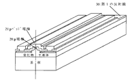
電極形成後、ウェーハをCVD装置に移送し、p電極20、n電極22、p型クラッド層10等、基板から上の表面に露出している層全てに渡って、SiO2とTiO2の誘電体多層膜よりなる第1の反射鏡30を形成する。第1の反射鏡30の各層の膜厚はλ/4n(λ:活性層の発光波長、n:材料の屈折率)に従うものとする。第1の反射鏡30形成後の断面図を図6に示す。この第1の反射鏡は共振面側では活性層の発光を反射する反射鏡として作用し、さらに、n型コンタクト層3、p型クラッド層10の表面では電極間の短絡を防止する絶縁膜として作用する。このように、第1の反射鏡30を共振面と共振面との間に連続して形成することにより、非常に効果的に素子を作製することができる。反射鏡の材料としては例えばSiO2、TiO2、ZrO2、Al2O3、ZnO、MgO、ポリイミドのような高誘電体材料を用いることができる。
【0042】
第1の反射鏡30形成後、p電極20と、n電極22の表面に形成されている第1の反射鏡30を除去する。除去されて露出したp電極20と、n電極22の表面には電極面積を広げ、電流を均一に拡散させる目的で、それぞれpパッド電極21と、nパッド電極22とを図3に示すような構造となるように形成する。なお、図3に示すようにpパッド電極は、絶縁膜としての第1の反射鏡を介して、p型クラッド層10の表面にも渡って形成する。
【0043】
(劈開工程)
次に、ウェーハを研磨装置に移送し、ダイヤモンド研磨剤を用いて、窒化物半導体を形成していない側のサファイア基板をラッピングし、基板の厚さを50μmとする。ラッピング後、さらに細かい研磨剤で1μmポリシングして基板表面を鏡面状とする。基板の厚さは70μm以下、さらに好ましくは60μm以下、最も好ましくは50μm以下とすることにより、素子の放熱性が高まり素子が長寿命になる。
【0044】
基板研磨後、研磨面側をスクライブして、図6に示す一点鎖線の位置で、共振面に平行な方向でバー状に劈開し、劈開面に共振器を作製する。これにより、劈開面とエッチング面とで構成された共振器長550μmの共振面が作製される。なお劈開面はサファイア基板の上に成長した窒化物半導体面のM面とする。M面とは前にも説明したが、具体的には、図4に示すように、窒化物半導体を正六角柱の六方晶系で近似した場合に、その六角柱の側面に相当する四角形の面に相当する面である。なお、M面で劈開するためには、予めエッチング工程で作製する共振面がM面となるように作製しておく必要がある。さらにn電極に平行な位置でウェーハを切断することにより、図2に示すような形状のレーザ素子を得る。
【0045】
以上のようにしてレーザ素子を作製することにより、図1に示すような構造の素子を作製することができる。このレーザ素子の共振面の一方は劈開により形成されて、その劈開面には反射鏡が形成されていない。もう一方の共振面はエッチングにより形成され、そのエッチング面には反射鏡が形成されている。このレーザ素子をフェースアップ(基板とヒートシンクとが対向した状態)でヒートシンクに設置し、それぞれの電極をワイヤーボンディングして、室温でレーザ発振を試みたところ、室温において、閾値電流密度1.5kA/cm2、閾値電圧6Vで、発振波長405nmの連続発振が確認された。なお、劈開面側から出射されたレーザ光の出力は、両方の共振面をエッチングにより形成し、さらにその共振面に同一反射率を有する反射鏡を形成したものに比較して、およそ2倍に向上した。また劈開面側から周されたレーザ光のファーフィールドパターンも、楕円形であって乱れのない非常に奇麗な形状のものが得られた。
【0046】
[実施例2]
実施例1において、劈開工程終了後、劈開面以外の第1の反射鏡の表面にマスクを形成し、劈開面に同じくSiO2とTiO2の誘電体多層膜よりなる第2の反射鏡31を形成する。なお第2の反射鏡31はその膜厚を調整することにより、第1の反射鏡の反射率の1/10に調整する。
【0047】
第2の反射鏡形成後、マスクを除去し、同様にしてp電極20、n電極22の表面を露出させ、後は同様にしてレーザ素子を作製した。このレーザ素子の構造を示す概略的な断面図を図7に示す。このレーザ素子も同様に室温において連続発振を示し、実施例1のものに比較して出力がおよそ20%低下した。
【0048】
[実施例3]
実施例1のエッチング工程において、共振器長550μmとなるようにエッチングする他は同様にしてエッチングを行う。
【0049】
次に、同様にしてp型コンタクト層11にp電極20、n型コンタクト層3にn電極22を形成する。
【0050】
電極形成後、片方の共振面となるエッチング面にマスクを形成した後、ウェーハをCVD装置に移送し、実施例1と同様に基板から上の表面に露出している層全てに渡って、SiO2とTiO2の誘電体多層膜よりなる第1の反射鏡を形成する。このように、共振面形成後、窒化物半導体層の表面と共振面とに、連続した誘電体よりなる反射鏡を形成する工程を備えることにより、前述したように第1の反射鏡が窒化物半導体表面に形成された絶縁膜として作用し、電極間のショートを防止すると共に、p電極20の上にpパッド電極21を形成して、実質的な電極面積を広げることができる。電極面積が広がると閾値を低下させることができる。
【0051】
その後、マスクを除去した後、共振面と共振面との間でウェーハを劈開する。このようにして、エッチングにより両方の共振面が作製され、一方の共振面には反射鏡が形成されて、もう一方の共振面には反射鏡が形成されておらず、互いの共振面で反射率が異なるレーザ素子が作製できる。このレーザ素子は反射鏡が形成されていない側の共振面からレーザ光が取り出され、室温において、同様に閾値電流密度1.5kA/cm2、閾値電圧6Vで、発振波長405nmの連続発振が確認された。なお、反射鏡を形成していない共振面側から出射されたレーザ光の出力は、両方の共振面をエッチングにより形成し、さらにその共振面に同一反射率を有する反射鏡を形成したものに比較して、1.3倍に向上した。但し、レーザ光のファーフィールドパターンは劈開面でないために乱れがあった。しかし、この共振面より突出した平面部は研磨して除去するか、あるいは共振面に近い位置で基板を劈開することにより除去できる。
【0052】
【発明の効果】
以上説明したように、本発明のレーザ素子は互いの共振面の反射率を異ならせることにより、高出力なレーザ素子を実現することができる。しかも片方を劈開面、もう片方をエッチング面とすると、劈開面側から出射されるレーザ光はほぼ楕円形に近い非常に奇麗な形状のレーザ光が得られる。
【0053】
また本発明の製造方法では、反射鏡を作製する工程において、絶縁膜も形成することができるため、同一面側にあるレーザ素子の電極間ショートを防止でき、非常に信頼性の高い素子を実現できる。
【図面の簡単な説明】
【図1】 本発明の一実施例に係るレーザ素子の構造を示す概略断面図。
【図2】 図1のレーザ素子の形状を示す斜視図。
【図3】 図2のレーザ素子の構造を詳細に示す断面図。
【図4】 窒化物半導体の結晶構造を模式的に示すユニットセル図。
【図5】 本発明の製造方法の一工程において得られるウェーハの概略構造を示す部分断面図。
【図6】 本発明の製造方法の一工程において得られるウェーハの概略構造を示す部分断面図。
【図7】 本発明の他の実施例に係るレーザ素子の構造を示す概略断面図。
【符号の説明】
1・・・サファイア基板、
2・・・バッファ層、
3・・・n型コンタクト層、
4・・・クラック防止層、
5・・・n型クラッド層、
6・・・n型光ガイド層、
7・・・活性層、
8・・・p型キャップ層、
9・・・p型光ガイド層、
10・・・p型クラッド層、
11・・・p型コンタクト層、
20・・・p電極、
21・・・pパッド電極、
22・・・n電極、
23・・・nパッド電極、
30・・・第1の反射鏡、
31・・・第2の反射鏡。[0001]
BACKGROUND OF THE INVENTION
The present invention relates to a laser element made of a nitride semiconductor (In X Al Y Ga 1-XY N, 0 ≦ X, 0 ≦ Y, X + Y ≦ 1).
[0002]
[Prior art]
Nitride semiconductors have recently been put into practical use as full-color LED displays, traffic signal lights, and the like as materials for high-brightness blue LEDs and pure green LEDs. In addition, the present applicant recently announced a laser oscillation of 410 nm at room temperature at a pulse current using this material (for example, Document A: Jpn. J. Appl. Phys. Vol. 35 (1996) pp. L217). -L220, Literature B: Appl. Phys. Lett. 69 (10), 2 Sep. 1996 pp.1477-1479, etc.)
[0003]
A resonance surface of a laser element made of a nitride semiconductor is generally formed using a technique such as etching or cleavage. In Document A, the nitride semiconductor is etched to form an opposing resonant surface, and in B, the nitride semiconductor is grown on the sapphire A surface and cleaved by the R surface of the sapphire, thereby forming the resonant surface. Is forming. However, the output of these laser elements is still low and not satisfactory.
[0004]
[Problems to be solved by the invention]
Accordingly, the present invention has been made in view of such circumstances, and a main object thereof is to provide a laser element made of a nitride semiconductor with improved output and a method for manufacturing the same.
[0005]
[Means for Solving the Problems]
The nitride semiconductor laser device according to the present invention has a double heterostructure in which an n-type layer, an active layer, and a p-type layer each made of a nitride semiconductor are stacked on a substrate, and the nitride semiconductor layers face each other. In a nitride semiconductor laser device having an end surface as a resonance surface,
One of the resonance surfaces is an etching surface, and the other is a cleavage surface of a nitride semiconductor,
A striped ridge is formed in the p-type layer, and a p-electrode is formed on the top of the ridge.
A reflecting mirror made of a dielectric is continuously formed on the surface of the nitride semiconductor layer on the substrate including the etched surface;
A p-pad electrode connected to the p-electrode is formed over the surface of the p-type layer via the reflecting mirror .
[0006]
A second reflecting mirror may be formed on the cleavage plane.
[0007]
The reflecting mirror may be formed of one or more of SiO 2 , TiO 2 , ZrO 2 , and polyimide.
[0008]
An n-layer plane at a position substantially perpendicular to the resonance surface may be exposed on the etching resonance surface.
[0009]
The other resonance surface is an M-plane nitride semiconductor.
[0010]
A reflection mirror that reflects laser light into the nitride semiconductor layer is formed on the cleavage surface, and the reflectance of the reflection mirror formed on the etching surface is greater than the reflectance of the reflection mirror formed on the cleavage surface. Is preferably adjusted to be high.
[0011]
A method for manufacturing a nitride semiconductor laser device according to the present invention includes:
Laminating an n-type layer, an active layer, and a p-type layer each made of a nitride semiconductor on a substrate;
Etching the p-type layer to form a striped ridge;
Etching the p-type layer and active layer, respectively to form an etching end surface facing the resonance surface, Ru expose the n-type layer step,
Forming a p-electrode on the top of the ridge;
Forming a reflecting mirror made of a dielectric film over all layers exposed above the substrate, including on the p-electrode;
Removing the reflecting mirror on the p-electrode;
Forming a p-pad electrode connected to the p-electrode across the surface of the p-type layer via the reflecting mirror;
And cleaving the nitride semiconductor between the mutually opposing resonant surfaces.
[0012]
After cleaving the nitride semiconductor, another reflecting mirror having a lower reflectance of the emission wavelength of the active layer than the reflecting mirror formed on the etched surface may be formed on the cleaved surface.
[0013]
A step of providing a second reflecting mirror on the cleavage surface of the nitride semiconductor may be provided after the step of cleaving the nitride semiconductor.
[0015]
DETAILED DESCRIPTION OF THE INVENTION
FIG. 1 is a perspective view showing the shape of the laser element of the present invention, and FIG. 2 is a schematic cross-sectional view of the laser element of FIG. 1 cut in parallel with the resonance direction at a position indicated by a one-dot chain line. The basic structure is a double hetero structure in which an n-type layer, an active layer, and a p-type layer made of a nitride semiconductor are stacked on a substrate, and the end faces of these nitride semiconductor layers are opposed to each other. Has a surface. These resonant surfaces have different reflectivities at the emission wavelength of the active layer. As a specific resonance surface, one is an etching surface of a nitride semiconductor, and the other is a cleavage surface of the nitride semiconductor.
[0016]
In order to etch the nitride semiconductor, there are methods such as wet etching and dry etching, but dry etching is preferably used to form a smooth surface as a resonance surface. Dry etching includes, for example, reactive ion etching (RIE), reactive ion beam etching (RIBE), electron cyclotron etching (ECR), ion beam etching, and the like. The nitride semiconductor can be etched to form a resonant surface. For example, Japanese Patent Laid-Open No. 8-17803 previously disclosed by the present applicant discloses a specific means for etching a nitride semiconductor.
[0017]
On the other hand, in order to form a resonance surface on the end face of a nitride semiconductor by cleavage, for example, as described in Japanese Patent Laid-Open No. 8-153931 previously disclosed by the present applicant, a C-axis orientation is formed on the C surface of sapphire. After growing the nitride semiconductor, there is a method of dividing the sapphire substrate by the M plane. In addition, there is a method of growing a nitride semiconductor on the sapphire A surface and cleaving on the R surface of the sapphire as described in the above document B. In the laser element of the present invention, the plane orientation of the cleavage plane of the nitride semiconductor is not particularly limited. However, preferably, when the M plane of the nitride semiconductor is the resonance plane, a resonance plane close to a mirror surface can be obtained with very good yield. It is done. In addition, the resonance surface as used in the field of this invention refers to the resonance surface formed in the end surface of an active layer, as shown by the arrow of FIG.
[0018]
Thus, the reflectance of the resonant surface of the laser element can be made different by making one resonant surface of the nitride semiconductor an etched surface and the other resonant surface an etched surface. The output of laser light emitted from a low resonance surface can be improved. In particular, as shown in FIGS. 1 and 2, when the first reflecting mirror that reflects the emission wavelength of the active layer is formed on the resonance surface on the etching surface side, the reflectance on the cleavage surface side is further reduced. Since light is directly emitted, a laser element with high output can be obtained.
[0019]
Furthermore, when the resonance surface is formed by etching, as shown in FIG. 1, the plane of the n layer at a position substantially perpendicular to the resonance surface is exposed on the etching resonance surface side. This plane reflects the laser light at its surface and disturbs the far field pattern of the laser light. That is, if there is a plane protruding from the resonance surface on the laser emission light side, the shape of the laser beam is disturbed on that plane. On the other hand, in the case of a cleavage plane, since there is no protruding portion, laser light having a fixed shape close to an ellipse can be obtained. Therefore, in the laser element of the present invention, it is desirable to mainly extract laser light emitted from the cleavage plane side and use it as various light sources.
[0020]
More preferably, as shown in FIG. 1, it is most desirable to form the first reflecting mirror on the etching surface side and not to form the reflecting mirror on the cleavage surface side. When the laser beam is emitted from the resonance surface, the reflection mirror partially blocks the emission. Therefore, by not forming a reflecting mirror on the cleavage plane side, light extraction efficiency is improved and slope efficiency is improved, so that a high-power laser can be obtained. More preferably, the reflecting mirror is made of a high dielectric material such as SiO 2 , TiO 2 , ZrO 2 , or polyimide, which is very convenient in the manufacturing method of the present invention. That is, in the case of a nitride semiconductor laser element, the p-electrode and the n-electrode are often taken out from the semiconductor layer on the same surface side, and therefore, a very short circuit between the electrodes is very careful when forming the electrode. Cost. However, when a reflecting mirror made of a high dielectric material is formed with a resonance surface as in the present invention, the reflecting mirror acts as an insulating film that prevents the n and p electrodes from short-circuiting, so that the reliability of the laser element is improved. To do. The operation of the reflecting mirror made of a dielectric will be further described in detail in the present embodiment.
[0021]
In the laser element of the present invention, a second reflecting mirror having a reflectance lower than that of the first reflecting mirror formed on the etching surface side may be formed on the cleavage surface side. When the second reflecting mirror is formed, there is an advantage that the threshold value is lowered. However, the output of the laser element emitted from the cleavage plane side is slightly lowered as compared with the case where the second reflecting mirror is not formed.
[0022]
【Example】
Next, the present invention will be described in detail in Examples. FIG. 3 is a schematic cross-sectional view showing one structure of the laser device of the present invention, and shows the structure when the device is cut in a direction parallel to the resonance surface. FIG. 4 is a block cell diagram showing the crystal structure of a nitride semiconductor. 5 and 6 are partial cross-sectional views showing the structure of the laser device obtained in one step of the embodiment of the present invention. This figure is a view when the device is cut in a direction parallel to the resonance direction of the laser beam. Show. The laser element and the manufacturing method of the present invention will be described below based on these drawings.
[0023]
[Example 1]
Hereinafter, a method for manufacturing the laser element having the structure shown in FIG. 3 will be described.
(Lamination process)
1) On the
2) GaN buffer layer 2
3) Contact layer 3 made of Si-doped n-type GaN
4) Crack prevention layer 4 made of Si-doped n-type In0.1Ga0.9N
5) n-type cladding layer 5 made of Si-doped n-type Al0.2Ga0.8N
6) n-type light guide layer 6 made of Si-doped GaN
7) Active layer 7 in which three pairs of well layers made of Si-doped In0.2Ga0.8N and 25 angstroms of barrier layers made of Si-doped In0.01Ga0.95N are laminated, and finally the well layer is laminated.
8) p-type cap layer 8 made of Mg-doped p-type Al0.1Ga0.9N
9) p-type light guide layer 9 made of Mg-doped p-type GaN
10) p-type cladding layer 10 made of Mg-doped p-type Al0.2Ga0.8N
11) p-type contact layer 11 made of Mg-doped p-type GaN
Are sequentially stacked.
[0024]
1) As the
[0025]
2) The buffer layer 2 can be formed of AlN, GaN, AlGaN or the like at a temperature of 900 ° C. or less and with a film thickness of several tens of angstroms to several hundreds of angstroms. This buffer layer is formed to mitigate the irregularity of the lattice constant between the substrate and the nitride semiconductor, but may be omitted depending on the growth method of the nitride semiconductor, the type of the substrate, and the like.
[0026]
3) n-type contact layer 3 may be composed of In X Al Y Ga 1-XY N (0 ≦ X, 0 ≦ Y, X + Y ≦ 1), in particular doped GaN, InGaN, a Si or Ge among them By comprising GaN, an n-type layer with a high carrier concentration can be obtained, and a preferable ohmic contact with the n electrode can be obtained.
[0027]
4) The crack prevention layer 4 is grown on an n-type nitride semiconductor containing In, preferably InGaN, so that an n-type cladding layer containing Al to be grown next can be grown in a thick film. preferable. In the case of LD, it is necessary to grow a layer serving as a light confinement layer with a thickness of preferably 0.1 μm or more. Conventionally, when a thick AlGaN film is grown directly on a GaN or AlGaN layer, it was difficult to fabricate the device because a crack occurred in the AlGaN grown later, but this crack prevention layer is grown next. It is possible to prevent cracks from entering the n-type clad layer containing Al. The crack prevention layer is preferably grown with a film thickness of 100 Å or more and 0.5 μm or less. If it is thinner than 100 angstroms, it is difficult to act as crack prevention as described above, and if it is thicker than 0.5 μm, the crystal itself tends to turn black. This crack prevention layer can be omitted depending on conditions such as a growth method and a growth apparatus, but it is preferable to grow it when manufacturing an LD. This crack prevention layer may be grown in the n-type contact layer.
[0028]
5) The n-type cladding layer 5 acts as a carrier confinement layer and an optical confinement layer, and it is desirable to grow a nitride semiconductor containing Al, preferably AlGaN, and is 100 angstroms or more and 2 μm or less, more preferably 500 angstroms or more. By growing at 1 μm or less, a carrier confinement layer with good crystallinity can be formed.
[0029]
6) The n-type light guide layer 6 acts as a light guide layer of the active layer, and it is desirable to grow GaN and InGaN, and it is usually grown with a film thickness of 100 Å to 5 μm, more preferably 200 Å to 1 μm. Is desirable.
[0030]
7) The active layer 7 is formed by stacking a well layer made of a nitride semiconductor containing In having a thickness of 70 angstroms or less and a barrier layer made of a nitride semiconductor having a band gap energy larger than that of a well layer having a thickness of 150 angstroms or less. When a multi-quantum well structure is used, laser oscillation is likely to occur.
[0031]
8) Although the cap layer 8 is p-type, since the film thickness is thin, it may be i-type in which carriers are compensated by doping n-type impurities, and most preferably p-type. The thickness of the p-type cap layer is adjusted to 0.1 μm or less, more preferably 500 angstroms or less, and most preferably 300 angstroms or less. This is because if the film is grown to a thickness greater than 0.1 μm, cracks are likely to occur in the p-type cap layer, and a nitride semiconductor layer with good crystallinity is difficult to grow. Also, carriers cannot pass through this energy barrier due to the tunnel effect. When the AlGaN having a larger Al composition ratio is formed thinner, the LD element tends to oscillate. For example, if the Y value is AlYGa1-YN of 0.2 or more, it is desirable to adjust it to 500 angstroms or less. The lower limit of the film thickness of the p-type cap layer 8 is not particularly limited, but it is desirable to form the p-type cap layer 8 with a film thickness of 10 angstroms or more.
[0032]
9) As with the n-type light guide layer, the p-type light guide layer 9 is preferably grown using GaN or InGaN. This layer also functions as a buffer layer for growing the p-type cladding layer, and functions as a preferable light guide layer by growing it at a film thickness of 100 angstroms to 5 μm, more preferably 200 angstroms to 1 μm.
[0033]
10) As with the n-type cladding layer, the p-type cladding layer 10 functions as a carrier confinement layer and an optical confinement layer, and it is desirable to grow a nitride semiconductor containing Al, preferably AlGaN, which is 100 angstroms or more and 2 μm or less. More preferably, the carrier confinement layer having good crystallinity can be formed by growing at a thickness of 500 Å to 1 μm. Furthermore, it is preferable to make this layer a nitride semiconductor layer containing Al as described above, because a difference in contact resistance between the p-type contact layer and the p-electrode can be obtained.
[0034]
In the case of an active layer having a quantum structure having a well layer made of InGaN as in this embodiment, a p-type cap layer containing Al having a thickness of 0.1 μm or less is provided in contact with the active layer, and the p-type cap layer A p-type light guide layer having a bad gap energy smaller than that of the p-type cap layer is provided at a position farther from the active layer than the p-type light guide layer, and the p-type light guide layer is located at a position farther from the active layer than the p-type light guide layer. It is very preferable to provide a p-type cladding layer made of a nitride semiconductor containing Al having a larger band gap. Moreover, since the thickness of the p-type cap layer is set as thin as 0.1 μm or less, it does not act as a barrier for carriers, and holes injected from the p-layer pass through the p-type cap layer by the tunnel effect. Therefore, the recombination is efficiently performed in the active layer, and the output of the LD is improved. That is, since the injected carrier has a large band gap energy of the p-type cap layer, the carrier does not overflow the active layer even if the temperature of the semiconductor element rises or the injected current density increases, and the p-type cap layer does not overflow. Since it is blocked by the cap layer, carriers are stored in the active layer and light can be emitted efficiently. Therefore, even if the temperature of the semiconductor element rises, the light emission efficiency is hardly lowered, and an LD with a low threshold current can be realized.
[0035]
11) The p-type contact layer 11 can be composed of p-type In X Al Y Ga 1-XY N (0 ≦ X, 0 ≦ Y, X + Y ≦ 1), preferably Mg-doped GaN. The most preferable ohmic contact with the p-
[0036]
After laminating the nitride semiconductor layer including the active layer 7 on the
[0037]
Next, a mask having a predetermined shape is formed on the surface of the uppermost p-type contact layer, and the uppermost p-type contact layer 11 and the p-type contact layer 11 are formed by an RIE (reactive ion etching) apparatus as shown in FIG. The mold cladding layer 10 is mesa-etched to form a ridge shape having a stripe width of 4 μm.
[0038]
After the formation of the ridge, a mask is formed on the exposed p-type layer plane, and the plane of the n-type contact layer 22 is exposed symmetrically with respect to the stripe-shaped ridge as shown in FIG. Thus, by providing the n-type contact layer 3 on which the n-electrode 22 is to be formed symmetrically with respect to the ridge stripe, the current from the n-layer is uniformly applied to the active layer, and the threshold value is lowered. .
[0039]
(Etching process)
Next, a mask having a predetermined shape is formed on the surface of the n-type contact layer 3 and the exposed surface of the p-type layer, and the height is substantially the same as the plane of the n-type contact 3 by using RIE. Etching is performed to form a resonance surface having a resonator length of 700 μm.
[0040]
Next, an ohmic p-
[0041]
(First reflecting mirror forming step)
After the electrodes are formed, the wafer is transferred to a CVD apparatus, and the dielectric layers of SiO 2 and TiO 2 are spread over all layers exposed on the upper surface from the substrate, such as the
[0042]
After the formation of the first reflecting mirror 30, the first reflecting mirror 30 formed on the surfaces of the p-
[0043]
(Cleaving process)
Next, the wafer is transferred to a polishing apparatus, and the sapphire substrate on the side where the nitride semiconductor is not formed is lapped with a diamond abrasive so that the thickness of the substrate is 50 μm. After lapping, the substrate surface is mirror-finished by polishing with 1 μm with a finer abrasive. By setting the thickness of the substrate to 70 μm or less, more preferably 60 μm or less, and most preferably 50 μm or less, the heat dissipation of the device is enhanced and the device has a long life.
[0044]
After polishing the substrate, the polished surface side is scribed, and cleaved into a bar shape in the direction parallel to the resonance surface at the position of the alternate long and short dash line shown in FIG. 6 to produce a resonator on the cleavage surface. As a result, a resonant surface having a resonator length of 550 μm constituted by a cleavage plane and an etched surface is produced. Note that the cleavage plane is the M plane of the nitride semiconductor surface grown on the sapphire substrate. Although the M plane has been described before, specifically, as shown in FIG. 4, when a nitride semiconductor is approximated by a hexagonal system of regular hexagonal columns, a rectangular surface corresponding to the side of the hexagonal column It is a surface corresponding to. Note that, in order to cleave at the M plane, it is necessary to prepare in advance such that the resonance plane produced by the etching process becomes the M plane. Further, by cutting the wafer at a position parallel to the n-electrode, a laser element having a shape as shown in FIG. 2 is obtained.
[0045]
By manufacturing a laser element as described above, an element having a structure as shown in FIG. 1 can be manufactured. One of the resonance surfaces of the laser element is formed by cleavage, and no reflecting mirror is formed on the cleavage surface. The other resonance surface is formed by etching, and a reflecting mirror is formed on the etching surface. This laser element was placed face up (with the substrate and the heat sink facing each other) on the heat sink, and each electrode was wire-bonded and laser oscillation was attempted at room temperature. At room temperature, the threshold current density was 1.5 kA / Continuous oscillation with an oscillation wavelength of 405 nm was confirmed at cm 2 and a threshold voltage of 6 V. Note that the output of the laser light emitted from the cleavage plane side is approximately twice that of the case where both resonant surfaces are formed by etching and a reflecting mirror having the same reflectance is formed on the resonant surfaces. Improved. In addition, the far field pattern of the laser light that was circulated from the cleavage plane side was elliptical and had a very beautiful shape with no disturbance.
[0046]
[Example 2]
In Example 1, after completion of the cleavage process, a mask is formed on the surface of the first reflecting mirror other than the cleavage plane, and the second reflecting mirror 31 made of a dielectric multilayer film of SiO 2 and TiO 2 is formed on the cleavage plane. Form. The second reflecting mirror 31 is adjusted to 1/10 of the reflectance of the first reflecting mirror by adjusting its film thickness.
[0047]
After the formation of the second reflecting mirror, the mask was removed and the surfaces of the p-
[0048]
[Example 3]
Etching is performed in the same manner as in the etching process of Example 1 except that the resonator length is 550 μm.
[0049]
Next, a p-
[0050]
After the electrode is formed, a mask is formed on the etching surface serving as one of the resonance surfaces, and then the wafer is transferred to the CVD apparatus, and the SiO 2 layer is exposed over the entire surface exposed from the substrate in the same manner as in Example 1. A first reflecting mirror made of a dielectric multilayer film of 2 and TiO 2 is formed. Thus, after forming the resonance surface, the first reflection mirror is nitrided as described above by providing a step of forming a reflection mirror made of a continuous dielectric material on the surface of the nitride semiconductor layer and the resonance surface. It acts as an insulating film formed on the semiconductor surface, prevents a short circuit between the electrodes, and forms a p-
[0051]
Thereafter, after removing the mask, the wafer is cleaved between the resonance surfaces. In this way, both resonance surfaces are produced by etching, a reflection mirror is formed on one resonance surface, a reflection mirror is not formed on the other resonance surface, and reflection is performed on each resonance surface. Laser elements having different rates can be manufactured. In this laser element, laser light is extracted from the resonance surface on the side where the reflecting mirror is not formed, and continuous oscillation with a threshold current density of 1.5 kA / cm 2 and a threshold voltage of 6 V is confirmed at room temperature. It was done. The output of the laser beam emitted from the resonance surface side where the reflecting mirror is not formed is compared with that in which both resonance surfaces are formed by etching and a reflecting mirror having the same reflectance is formed on the resonance surface. And improved 1.3 times. However, the far-field pattern of the laser beam was not a cleavage plane and thus was disturbed. However, the flat portion protruding from the resonance surface can be removed by polishing or by cleaving the substrate at a position close to the resonance surface.
[0052]
【The invention's effect】
As described above, the laser element of the present invention can realize a high-power laser element by making the reflectances of the resonance surfaces different from each other. In addition, when one side is a cleavage plane and the other side is an etching surface, the laser beam emitted from the cleavage plane side can be a laser beam having a very beautiful shape that is almost elliptical.
[0053]
In the manufacturing method of the present invention, an insulating film can also be formed in the process of manufacturing the reflecting mirror, so that it is possible to prevent a short circuit between the electrodes of the laser element on the same surface side, and to realize a highly reliable element. it can.
[Brief description of the drawings]
FIG. 1 is a schematic cross-sectional view showing the structure of a laser device according to an embodiment of the present invention.
2 is a perspective view showing the shape of the laser element of FIG. 1. FIG.
3 is a cross-sectional view showing in detail the structure of the laser device of FIG. 2;
FIG. 4 is a unit cell diagram schematically showing a crystal structure of a nitride semiconductor.
FIG. 5 is a partial cross-sectional view showing a schematic structure of a wafer obtained in one step of the manufacturing method of the present invention.
FIG. 6 is a partial cross-sectional view showing a schematic structure of a wafer obtained in one step of the manufacturing method of the present invention.
FIG. 7 is a schematic cross-sectional view showing the structure of a laser device according to another embodiment of the present invention.
[Explanation of symbols]
1 ... sapphire substrate,
2 ... buffer layer,
3 ... n-type contact layer,
4 ... crack prevention layer,
5 ... n-type cladding layer,
6 ... n-type light guide layer,
7 ... active layer,
8 ... p-type cap layer,
9: p-type light guide layer,
10 ... p-type cladding layer,
11 ... p-type contact layer,
20 ... p electrode,
21 ... p pad electrode,
22 ... n electrode,
23 ... n pad electrode,
30: First reflecting mirror,
31: Second reflecting mirror.
Claims (9)
前記共振面の一方はエッチング面であり、他方は窒化物半導体の劈開面であり、
前記p型層にはストライプ状のリッジが形成され、該リッジの最上部にp電極が形成され、
誘電体からなる反射鏡が、前記エッチング面を含む基板上にある窒化物半導体層の表面に連続して形成され、
前記p電極と接続するpパッド電極が前記反射鏡を介してp型層の表面にも渡って形成されたことを特徴とする窒化物半導体レーザ素子。A nitride semiconductor laser device having a double hetero structure in which an n-type layer, an active layer, and a p-type layer each made of a nitride semiconductor are laminated on a substrate, and having opposite end faces of the nitride semiconductor layer as resonance surfaces In
One of the resonance surfaces is an etching surface, and the other is a cleavage surface of a nitride semiconductor,
A striped ridge is formed in the p-type layer, and a p-electrode is formed on the top of the ridge.
A reflecting mirror made of a dielectric is continuously formed on the surface of the nitride semiconductor layer on the substrate including the etched surface;
A nitride semiconductor laser device, wherein a p-pad electrode connected to the p-electrode is formed over the surface of the p-type layer via the reflecting mirror .
【外1】
前記p型層をエッチングしてストライプ状のリッジを形成する工程と、
前記p型層及び活性層をエッチングして、それぞれ共振面となる対向するエッチング端面を形成し、n型層を露出させる工程と、
前記リッジの最上部にp電極を形成する工程と、
前記p電極上を含む、前記基板から上に露出している層全てに渡って誘電体膜よりなる反射鏡を形成する工程と、
前記p電極上の反射鏡を除去する工程と、
前記p電極に接続するpパッド電極を、前記反射鏡を介してp型層の表面に渡って形成する工程と、
前記互いに対向する共振面の間において窒化物半導体を劈開する工程とを備えることを特徴とする窒化物半導体レーザ素子の製造方法。Laminating an n-type layer, an active layer, and a p-type layer each made of a nitride semiconductor on a substrate;
Etching the p-type layer to form a striped ridge;
Etching the p-type layer and active layer, respectively to form an etching end surface facing the resonance surface, Ru expose the n-type layer step,
Forming a p-electrode on the top of the ridge;
Forming a reflecting mirror made of a dielectric film over all layers exposed above the substrate, including on the p-electrode;
Removing the reflecting mirror on the p-electrode;
Forming a p-pad electrode connected to the p-electrode across the surface of the p-type layer via the reflecting mirror;
And a step of cleaving the nitride semiconductor between the mutually opposing resonant surfaces.
Priority Applications (1)
| Application Number | Priority Date | Filing Date | Title |
|---|---|---|---|
| JP2002040228A JP4370751B2 (en) | 2002-02-18 | 2002-02-18 | Nitride semiconductor laser device and manufacturing method thereof |
Applications Claiming Priority (1)
| Application Number | Priority Date | Filing Date | Title |
|---|---|---|---|
| JP2002040228A JP4370751B2 (en) | 2002-02-18 | 2002-02-18 | Nitride semiconductor laser device and manufacturing method thereof |
Related Parent Applications (1)
| Application Number | Title | Priority Date | Filing Date |
|---|---|---|---|
| JP33388496A Division JP3476636B2 (en) | 1996-12-13 | 1996-12-13 | Nitride semiconductor laser device |
Publications (3)
| Publication Number | Publication Date |
|---|---|
| JP2002252409A JP2002252409A (en) | 2002-09-06 |
| JP2002252409A5 JP2002252409A5 (en) | 2004-11-25 |
| JP4370751B2 true JP4370751B2 (en) | 2009-11-25 |
Family
ID=19192685
Family Applications (1)
| Application Number | Title | Priority Date | Filing Date |
|---|---|---|---|
| JP2002040228A Expired - Fee Related JP4370751B2 (en) | 2002-02-18 | 2002-02-18 | Nitride semiconductor laser device and manufacturing method thereof |
Country Status (1)
| Country | Link |
|---|---|
| JP (1) | JP4370751B2 (en) |
-
2002
- 2002-02-18 JP JP2002040228A patent/JP4370751B2/en not_active Expired - Fee Related
Also Published As
| Publication number | Publication date |
|---|---|
| JP2002252409A (en) | 2002-09-06 |
Similar Documents
| Publication | Publication Date | Title |
|---|---|---|
| JP4378070B2 (en) | Nitride semiconductor device | |
| JP3436128B2 (en) | Method for growing nitride semiconductor and nitride semiconductor device | |
| JP3346735B2 (en) | Nitride semiconductor light emitting device and method of manufacturing the same | |
| JP3491538B2 (en) | Method for growing nitride semiconductor and nitride semiconductor device | |
| JP5076656B2 (en) | Nitride semiconductor laser device | |
| JP3460581B2 (en) | Method for growing nitride semiconductor and nitride semiconductor device | |
| JP3375042B2 (en) | Nitride semiconductor laser device | |
| JP4665394B2 (en) | Nitride semiconductor laser device | |
| JP4043087B2 (en) | Nitride semiconductor device manufacturing method and nitride semiconductor device | |
| JP4873116B2 (en) | Nitride semiconductor laser device and manufacturing method thereof | |
| JP3314641B2 (en) | Nitride semiconductor laser device | |
| JPH11191637A (en) | Nitride semiconductor device | |
| JP3604278B2 (en) | Nitride semiconductor laser device | |
| JPH11195812A (en) | Nitride semiconductor light-emitting element | |
| JP4639571B2 (en) | Nitride semiconductor laser device and manufacturing method thereof | |
| JP3216118B2 (en) | Nitride semiconductor device and method of manufacturing the same | |
| JP3537984B2 (en) | Nitride semiconductor laser device | |
| JP4370751B2 (en) | Nitride semiconductor laser device and manufacturing method thereof | |
| JP2005101536A (en) | Nitride semiconductor laser element | |
| JP3476636B2 (en) | Nitride semiconductor laser device | |
| JP3278108B2 (en) | Method for manufacturing nitride semiconductor laser element | |
| JP3800146B2 (en) | Method of manufacturing nitride semiconductor device | |
| JP4954407B2 (en) | Nitride semiconductor light emitting device | |
| JP2001320130A (en) | Nitride semiconductor laser device and manufacturing method of it | |
| JP4321295B2 (en) | Manufacturing method of nitride semiconductor laser device |
Legal Events
| Date | Code | Title | Description |
|---|---|---|---|
| A521 | Written amendment |
Free format text: JAPANESE INTERMEDIATE CODE: A523 Effective date: 20031209 |
|
| A621 | Written request for application examination |
Free format text: JAPANESE INTERMEDIATE CODE: A621 Effective date: 20031209 |
|
| A521 | Written amendment |
Free format text: JAPANESE INTERMEDIATE CODE: A821 Effective date: 20060308 |
|
| RD02 | Notification of acceptance of power of attorney |
Free format text: JAPANESE INTERMEDIATE CODE: A7422 Effective date: 20060308 |
|
| RD04 | Notification of resignation of power of attorney |
Free format text: JAPANESE INTERMEDIATE CODE: A7424 Effective date: 20060321 |
|
| RD03 | Notification of appointment of power of attorney |
Free format text: JAPANESE INTERMEDIATE CODE: A7423 Effective date: 20080131 |
|
| A131 | Notification of reasons for refusal |
Free format text: JAPANESE INTERMEDIATE CODE: A131 Effective date: 20080603 |
|
| A521 | Written amendment |
Free format text: JAPANESE INTERMEDIATE CODE: A523 Effective date: 20080804 |
|
| TRDD | Decision of grant or rejection written | ||
| A01 | Written decision to grant a patent or to grant a registration (utility model) |
Free format text: JAPANESE INTERMEDIATE CODE: A01 Effective date: 20090811 |
|
| A01 | Written decision to grant a patent or to grant a registration (utility model) |
Free format text: JAPANESE INTERMEDIATE CODE: A01 |
|
| A61 | First payment of annual fees (during grant procedure) |
Free format text: JAPANESE INTERMEDIATE CODE: A61 Effective date: 20090824 |
|
| FPAY | Renewal fee payment (event date is renewal date of database) |
Free format text: PAYMENT UNTIL: 20120911 Year of fee payment: 3 |
|
| R150 | Certificate of patent or registration of utility model |
Free format text: JAPANESE INTERMEDIATE CODE: R150 |
|
| FPAY | Renewal fee payment (event date is renewal date of database) |
Free format text: PAYMENT UNTIL: 20120911 Year of fee payment: 3 |
|
| FPAY | Renewal fee payment (event date is renewal date of database) |
Free format text: PAYMENT UNTIL: 20120911 Year of fee payment: 3 |
|
| FPAY | Renewal fee payment (event date is renewal date of database) |
Free format text: PAYMENT UNTIL: 20130911 Year of fee payment: 4 |
|
| R250 | Receipt of annual fees |
Free format text: JAPANESE INTERMEDIATE CODE: R250 |
|
| R250 | Receipt of annual fees |
Free format text: JAPANESE INTERMEDIATE CODE: R250 |
|
| R250 | Receipt of annual fees |
Free format text: JAPANESE INTERMEDIATE CODE: R250 |
|
| LAPS | Cancellation because of no payment of annual fees |