JP4366173B2 - Image forming apparatus - Google Patents
Image forming apparatus Download PDFInfo
- Publication number
- JP4366173B2 JP4366173B2 JP2003369718A JP2003369718A JP4366173B2 JP 4366173 B2 JP4366173 B2 JP 4366173B2 JP 2003369718 A JP2003369718 A JP 2003369718A JP 2003369718 A JP2003369718 A JP 2003369718A JP 4366173 B2 JP4366173 B2 JP 4366173B2
- Authority
- JP
- Japan
- Prior art keywords
- developer
- carriers
- image
- carrier
- developing
- Prior art date
- Legal status (The legal status is an assumption and is not a legal conclusion. Google has not performed a legal analysis and makes no representation as to the accuracy of the status listed.)
- Expired - Fee Related
Links
Images


Classifications
-
- G—PHYSICS
- G03—PHOTOGRAPHY; CINEMATOGRAPHY; ANALOGOUS TECHNIQUES USING WAVES OTHER THAN OPTICAL WAVES; ELECTROGRAPHY; HOLOGRAPHY
- G03G—ELECTROGRAPHY; ELECTROPHOTOGRAPHY; MAGNETOGRAPHY
- G03G15/00—Apparatus for electrographic processes using a charge pattern
- G03G15/01—Apparatus for electrographic processes using a charge pattern for producing multicoloured copies
- G03G15/0105—Details of unit
- G03G15/0126—Details of unit using a solid developer
-
- G—PHYSICS
- G03—PHOTOGRAPHY; CINEMATOGRAPHY; ANALOGOUS TECHNIQUES USING WAVES OTHER THAN OPTICAL WAVES; ELECTROGRAPHY; HOLOGRAPHY
- G03G—ELECTROGRAPHY; ELECTROPHOTOGRAPHY; MAGNETOGRAPHY
- G03G2215/00—Apparatus for electrophotographic processes
- G03G2215/01—Apparatus for electrophotographic processes for producing multicoloured copies
- G03G2215/0103—Plural electrographic recording members
- G03G2215/0119—Linear arrangement adjacent plural transfer points
-
- G—PHYSICS
- G03—PHOTOGRAPHY; CINEMATOGRAPHY; ANALOGOUS TECHNIQUES USING WAVES OTHER THAN OPTICAL WAVES; ELECTROGRAPHY; HOLOGRAPHY
- G03G—ELECTROGRAPHY; ELECTROPHOTOGRAPHY; MAGNETOGRAPHY
- G03G2215/00—Apparatus for electrophotographic processes
- G03G2215/01—Apparatus for electrophotographic processes for producing multicoloured copies
- G03G2215/019—Structural features of the multicolour image forming apparatus
- G03G2215/0193—Structural features of the multicolour image forming apparatus transfer member separable from recording member
Description
本発明は、電子写真方式或いは静電記録方式を用いた複写機、レーザービームプリンタなどの画像形成装置に関するものである。 The present invention relates to an image forming apparatus such as a copying machine or a laser beam printer using an electrophotographic system or an electrostatic recording system.
近年、例えば電子写真方式を用いた画像形成装置は、高速化、高機能化、カラー化が進められてきており、各種方式の画像形成装置が提案されている。又、高速化という観点からは、異なる色の画像を形成する複数の画像形成部(画像形成ユニット)を直列に配置し、これらを同時に駆動することによって画像形成を行うインライン方式の装置の研究、開発が進んでいる。このような装置は高速でカラー画像の形成が可能であることから、例えば高速印字の要望の高いビジネスユースなどにおいて極めて有用であると考えられる。 In recent years, for example, image forming apparatuses using an electrophotographic method have been increased in speed, function, and color, and various types of image forming apparatuses have been proposed. From the standpoint of speeding up, research on an inline system that forms images by arranging a plurality of image forming units (image forming units) that form images of different colors in series and simultaneously driving them, Development is progressing. Since such an apparatus can form a color image at high speed, it is considered to be extremely useful in, for example, business use where high-speed printing is highly demanded.
このインライン方式の画像形成装置には、被転写体として中間転写体上に一旦複数色の現像剤像(トナー像)を重ねあわせ1次転写し、これを一括して転写材、例えば、記録用紙、OHPシート、布などの上に2次転写して最終画像を形成する中間転写方式を用いるものがある。 In this in-line image forming apparatus, a plurality of color developer images (toner images) are once superimposed and transferred onto an intermediate transfer member as a transfer target, and then transferred to a transfer material such as a recording sheet. In some cases, an intermediate transfer method is used in which a final image is formed by secondary transfer onto an OHP sheet or cloth.
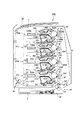
図8は、この種の画像形成装置の要部概略断面を示す。画像形成装置200は、複数の像形成手段として、例えば、イエロー(Y)、マゼンタ(M)、シアン(C)、ブラック(Bk)の各色の画像を形成するための第1〜第4の画像形成部PY、PM、PC、PBkを有する。そして、各画像形成部が備える像担持体としてのドラム型の電子写真感光体(以下、「感光ドラム」という。)10Y、10M、10C、10Bkに現像剤としてのトナーにより形成したトナー像を、各1次転写部N1において対応する1次転写手段26Y、26M、26C、26Bkの作用によって中間転写体31上に順次重ね合わせて1次転写し、その後、中間転写体31上のトナー像を2次転写部N2において、2次転写手段32の作用によって一括して転写材S上に転写する。この際、転写材Sは、表面側が中間転写体31に、又裏面側が2次転写手段32に接触するようにして、両者により挟持搬送される。
FIG. 8 shows a schematic cross section of the main part of this type of image forming apparatus. The
図8の画像形成装置200に即して、各画像形成部の動作を更に説明する。尚、各画像形成部の構成は、形成する画像の色が異なる他は実質的に同一構成とされるので、以下、特に区別を要しない場合は、各画像形成部に属する要素であることを示す添え字Y、M、C、Bkは省略して総括的に説明する。
The operation of each image forming unit will be further described with reference to the
各画像形成部において、図示矢印方向に回転駆動される感光ドラム10は、最初に、帯電手段としての帯電ローラ11との接触部で表面が一様に帯電され、次いで、露光手段(図示せず)によって表面に画像信号に応じた静電潜像が形成される。続いて、この静電潜像は、現像手段13によってトナーが付着されて現像され、感光ドラム10の表面に静電潜像に対応した可視画像が形成される。
In each image forming unit, the surface of the
帯電ローラ11は、その電極を介して高圧電源(図示せず)により電圧が印加されることにより、感光ドラム10の表面を一定の電位で一様に帯電させる。又、帯電ローラ11は、感光ドラム10の表面に所定の押圧力で圧接され、感光ドラム10の回転に伴い従動回転しながら感光ドラム10を帯電させる。
The
露光手段としての例えばレーザースキャナ(図示せず)は、画像信号源の画像信号により変調された光信号を供給し、一様に帯電された感光ドラム10の表面に光信号Lを与え、画像信号に対応した静電潜像を形成する。
For example, a laser scanner (not shown) as an exposure unit supplies an optical signal modulated by an image signal of an image signal source, gives an optical signal L to the uniformly charged surface of the
現像手段13としては、従来、現像剤を感光体に搬送する現像剤担持体としての現像ローラ16を感光ドラム10に接触させて現像を行うもの(以下、これを「接触現像方式」という。)がある。斯かる現像方式においては、感光ドラム10上に形成された静電潜像による明暗部電位と現像ローラ16に印加されるバイアス電圧との関係に基づいて、所定量のトナーを、感光ドラム10と現像ローラ16との接触部(現像部)において感光ドラム10上に形成された静電潜像側に移行付着させ、静電潜像に対応した可視画像を形成する。
As the developing means 13, conventionally, development is performed by bringing a developing
斯かる現像手段(現像装置)13は、感光ドラム10に接触する接触現像ローラ16、現像ローラ16にトナーを供給する現像剤供給部材としてのトナー供給ローラ18、現像ローラ16上に供給するトナーを規制する現像剤規制部材としての現像ブレード17を現像容器(現像装置本体)20内に有する。又、現像ブレード17へ電圧を印加する規制部材電圧印加手段としての高圧電源(ブレードバイアス電源)22a、22b、現像ローラ16及びトナー供給ローラ18へ電圧を印加する現像電圧印加手段としての高圧電源(現像バイアス電源)23Y、23M、23C、23Bkが設けられている。
Such developing means (developing device) 13 includes a
現像ローラ16は、感光ドラム10の表面に接触して感光ドラム10の回転に伴い回転するように構成され、現像容器20から一部外部に露出するように配置されている。
The developing
現像ブレード17は、現像ローラ16に当接するよう構成され、この現像ブレード17と現像ローラ16との当接部の間にトナーを通過させて規制することにより、現像ローラ16上にトナーの薄層を形成し、且つ、当接部での摩擦によりトナーに十分な摩擦帯電電荷(トリボ)を付与する。
The developing
又、トナー供給ローラ18は、現像装置13内において、現像ブレード17よりも現像ローラ16の回転方向上流側の位置で、現像ローラ16に当接して設けられており、図中矢印方向(現像ローラ16との接触部において現像ローラ16の表面移動方向とは逆方向)に回転することで現像ローラ16にトナーを供給する。
The
例えば、図8に示すレーザービームプリンタにあっては、複数色のトナー像を形成するために直列に配置した各画像形成部が、装置本体に対して着脱可能なプロセスカートリッジを有しているものである。即ち、回転駆動される像担持体としての感光ドラム10、感光ドラム10の表面を一様に帯電する帯電手段としての帯電ローラ11、静電潜像を現像剤としてのトナーによって現像して可視画像を形成する現像手段としての現像装置13、感光ドラム10をクリーニングするクリーニング手段としてのクリーニング装置14を枠体によって一体的にカートリッジ化し、これを装置本体に対して着脱可能にした各色のプロセスカートリッジ1Y、1M、1C、1Bkが、各画像形成部PY、PM、PC、PBkに配される。プロセスカートリッジは、この態様に限定されず、感光体を帯電させる帯電手段、感光体に現像剤を供給する現像手段、感光体をクリーニングするクリーニング手段のうち少なくとも1つと、感光体と、を一体的にカートリッジ化し、このカートリッジを画像形成装置本体に対して着脱可能としたものであればよい。斯かるプロセスカートリッジ方式によれば、例えば現像剤が無くなった際に操作者がプロセスカートリッジを交換することで、感光体など他の消耗品の交換をも行うことができ、飛躍的にメンテナンス性が向上する。
For example, in the laser beam printer shown in FIG. 8, each of the image forming units arranged in series to form toner images of a plurality of colors has a process cartridge that can be attached to and detached from the apparatus main body. It is. That is, the
又、このインライン方式では、常に多色刷り画像(例えば、4色フルカラー画像)の形成を行うだけとは限らず、例えば、黒単一の記録、即ち、モノクロ画像形成を行う頻度も高い。このような使用法に対処すべく、フルカラー画像形成と、モノクロ画像形成とを切り換えて行うことができるようにされた画像形成装置も提案されている。 In addition, in this in-line method, not only the formation of a multicolored image (for example, a four-color full-color image) is always performed, but, for example, a single black recording, that is, a monochrome image formation is frequently performed. In order to cope with such usage, there has also been proposed an image forming apparatus capable of switching between full-color image formation and monochrome image formation.
このように、インライン方式では、フルカラープリントを行うだけとは限らず、モノクロプリントを行うことがある。 As described above, in the in-line method, not only full-color printing but also monochrome printing may be performed.
図9及び10をも参照して更に説明する。図9及び10は、接触現像方式の現像装置13を用いた画像形成装置の一例における、感光ドラム10、現像装置13、1次転写手段26、中間転写体31などを特に示す要部構成図であり、他の要素は省略してある。
Further explanation will be made with reference to FIGS. FIGS. 9 and 10 are main part configuration diagrams specifically showing the
図9は、4色すべての画像形成部PY、PM、PC、PBkの現像装置13が稼働しているフルカラープリントモード時を示す。これに対して、モノクロプリントモード時には、図10に示すように、イエロー、マゼンタ、シアンの3色のプロセスカートリッジ1Y、1M、1Cの現像装置13Y、13M、13Cは停止し、ブラックのプロセスカートリッジ1Bkの現像装置13Bkのみ稼働している。この時、イエロー、マゼンタ、シアンの各画像形成部PY、PM、PCにおいて、1次転写手段26Y、26M、26Cが離間手段(図示せず)によって、感光ドラム10から離れる方向に移動され、これらの画像形成部PY、PM、PCにおいて中間転写体31は感光ドラム10から離間される。
FIG. 9 shows the full-color print mode in which the developing
一方、4色の濃度を調整するために、現像ローラ16へ現像バイアスを印加する電圧印加手段である現像バイアス電源23Y、23M、23C、23Bkは、独立して4つ必要である。
On the other hand, in order to adjust the density of the four colors, four development
又、現像ブレード17へバイアスを印加する電圧印加手段であるブレードバイアス電源22a、22bが2つ以上必要になる。これは、モノクロプリント時に、ブラック以外の3色の画像形成部PY、PM、PCの現像装置13Y、13M、13Cが停止した時に、現像ローラ16Y、16M、16Cへのバイアスを停止すると同時に、この3色の画像形成部PY、PM、PCにおける現像ブレード17へのバイアスも停止させなければならないからである。なぜなら、現像ローラ16へのバイアスが停止しているにも拘わらず現像ブレード17にバイアスを印加すると、現像ブレード17と現像ローラ16に挟まれたトナーは、停止中の現像ローラ16上で常にニップ内に留まり、通電劣化し、現像ブレード17に固着することがあるためである。現像ブレード17にトナーが固着してしまうと、現像ローラ16上のトナーコーティングを乱し、スジ画像が発生することがある。
Further, two or more blade
このように、上述した例における4色フルカラー画像形成の可能なインライン画像形成装置では、現像ブレード用のバイアス電源は、ブラック用と残り3色用の少なくとも2つ電源が必要であった。 As described above, in the in-line image forming apparatus capable of forming the four-color full color image in the above-described example, the bias power source for the developing blade needs at least two power sources for black and the remaining three colors.
しかし、電源が多いと、電装基盤の大型化やコストが増大するなどの短所がある。 However, when there are many power sources, there are disadvantages such as an increase in the size of the electrical equipment base and an increase in cost.
なお、インライン方式ではないものの、1つの現像ブレードへバイアスを印加することは、特許文献1にて知られている。
本発明の目的は、複数の現像剤規制部材に印加する電圧を共通化した画像形成装置を提供することである。 An object of the present invention is to provide an image forming apparatus in which voltages applied to a plurality of developer regulating members are shared.
本発明の他の目的は、複数の現像剤規制部材に電圧を印加する電圧印加手段を共通化し、小型化・低コスト化できる画像形成装置を提供することである。 Another object of the present invention is to provide an image forming apparatus in which a voltage applying unit that applies a voltage to a plurality of developer regulating members is shared, and the size and cost can be reduced.
本発明の他の目的は、モノクロのような特定色の画像形成も、フルカラーのような複数色の画像形成も、行うことができる画像形成装置を提供することである。 Another object of the present invention is to provide an image forming apparatus capable of performing image formation of a specific color such as monochrome and image formation of a plurality of colors such as full color.
本発明の他の目的は、複数の現像剤担持体のうち回転が停止した現像剤担持体に対して、現像剤規制部材へ現像剤が固着するのを防止し、現像スジを防止することのできる画像形成装置を提供することである。 Another object of the present invention is to prevent the developer from adhering to the developer regulating member and to prevent development streaks with respect to the developer carrying member whose rotation has stopped among a plurality of developer carrying members. An image forming apparatus is provided.
本発明の更なる目的及び特徴とするところは、添付図面を参照しつつ以下の詳細な説明を読むことにより一層明らかになるだろう。 Further objects and features of the present invention will become more apparent from the following detailed description when read in conjunction with the accompanying drawings.
上記目的は本発明に係る画像形成装置にて達成される。要約すれば、本発明は、像担持体に形成された静電像を現像剤で現像するために現像剤を担持搬送する現像剤担持体と、前記現像剤担持体に担持された現像剤を規制する現像剤規制部材と、をそれぞれが備える複数の現像装置と;前記複数の現像剤規制部材に共通電圧を印加する共通の電圧印加手段と;を有し、前記複数の現像剤担持体の全部が回転して画像形成を行なう第1の画像形成モードと、前記複数の現像剤担持体のうち第1の現像剤担持体が回転し、前記複数の現像剤担持体のうち前記第1の現像剤担持体以外の全部の現像剤担持体が回転しないで画像形成を行なう第2の画像形成モードと、を切り替え可能であり、前記第2の画像形成モードにおいて、前記複数の現像剤担持体のうち前記第1の現像剤担持体以外の全部の現像剤担持体の各電位と前記共通電圧との各電位差は、前記第1の現像剤担持体の電位と前記共通電圧との電位差よりも小さいことを特徴とする画像形成装置である。 The above object is achieved by the image forming apparatus according to the present invention. In summary, the present invention relates to a developer carrying member for carrying and conveying a developer for developing an electrostatic image formed on the image carrying member with a developer, and a developer carried on the developer carrying member. A plurality of developing devices each provided with a regulating member for regulating; a common voltage applying means for applying a common voltage to the plurality of developer regulating members; and a plurality of developer carrying members . A first image forming mode in which all the images are rotated to form an image; a first developer carrying member of the plurality of developer carrying members; and the first developer carrying member of the plurality of developer carrying members. It is possible to switch between a second image forming mode in which image formation is performed without rotation of all the developer carriers other than the developer carrier, and the plurality of developer carriers in the second image forming mode. Among all the developers other than the first developer carrier Each potential difference between the common voltage and the potential of the lifting body is an image forming apparatus, characterized in that less than the potential difference between the potential and the common voltage of the first developer carrying member.
本発明の一実施態様によると、前記複数の現像剤担持体に印加される電圧のそれぞれは、独立して変化可能である。本発明の他の実施態様によると、少なくとも前記複数の現像装置の現像動作中に、前記複数の現像剤担持体のそれぞれに電圧が印加されるとともに、前記複数の現像剤規制部材に前記電圧印加手段によって前記共通電圧が印加される。本発明の他の実施態様によると、前記複数の現像剤担持体に印加される電圧のそれぞれは、前記複数の現像剤担持体のそれぞれを用いて形成された参照画像のそれぞれの濃度の検知結果に応じて変化可能である。 According to an embodiment of the present invention, each of the voltages applied to the plurality of developer carriers can be changed independently. According to another embodiment of the present invention, at least during the developing operation of the plurality of developing devices, a voltage is applied to each of the plurality of developer carriers, and the voltage is applied to the plurality of developer regulating members. The common voltage is applied by means. According to another embodiment of the present invention, each of the voltages applied to the plurality of developer carriers is a detection result of a density of each reference image formed using each of the plurality of developer carriers. It can change depending on
本発明の一実施態様によると、回転が停止されていた前記複数の現像剤担持体のうち前記第1の現像剤担持体以外の全部の現像剤担持体を回転させるときに、前記複数の現像剤担持体のうち前記第1の現像剤担持体以外の全部の現像剤担持体に印加する電圧は、前記複数の現像剤担持体のうち前記第1の現像剤担持体以外の全部の現像剤担持体に現像時の電圧を印加する前に、現像時の電圧よりも現像剤の帯電極性と逆極性方向に近づけた電圧を印加する。本発明の他の実施態様によると、回転が停止されていた前記複数の現像剤担持体のうち前記第1の現像剤担持体以外の全部の現像剤担持体を回転させるときに、前記複数の現像剤担持体のうち前記第1の現像剤担持体以外の全部の現像剤担持体に印加する電圧は、前記複数の現像剤担持体のうち前記第1の現像剤担持体以外の全部の現像剤担持体に現像時の電圧を印加する前に、現像剤の帯電極性と逆極性の電圧を印加する。 According to an embodiment of the present invention, when rotating all the developer carriers other than the first developer carrier among the plurality of developer carriers that have stopped rotating, the plurality of developers The voltage applied to all the developer carriers other than the first developer carrier among the developer carriers is all the developers other than the first developer carrier among the plurality of developer carriers. Before applying the voltage at the time of development to the carrier, a voltage closer to the polarity opposite to the charging polarity of the developer than the voltage at the time of development is applied. According to another embodiment of the present invention, when rotating all the developer carriers other than the first developer carrier among the plurality of developer carriers whose rotation has been stopped, the plurality of developer carriers are rotated . The voltage applied to all the developer carriers other than the first developer carrier among the developer carriers is the same for all the developments other than the first developer carrier among the plurality of developer carriers. Before applying the developing voltage to the developer carrying member , a voltage having a polarity opposite to the charging polarity of the developer is applied.
本発明の他の態様によると、像担持体に形成された静電像を現像剤で現像するために現像剤を担持搬送する現像剤担持体と、前記現像剤担持体に担持された現像剤を規制する現像剤規制部材と、をそれぞれが備える複数の現像装置と;前記複数の現像剤規制部材に共通電圧を印加する共通の電圧印加手段と;前記複数の現像装置のそれぞれに対応する複数の像担持体と;を有し、前記複数の現像剤担持体のそれぞれは、前記複数の像担持体のそれぞれに接触可能であり、前記複数の現像剤担持体のうち第1の現像剤担持体以外の全部の現像剤担持体が現像動作を行なわないとき、前記複数の現像剤担持体のうち前記第1の現像剤担持体以外の全部の現像剤担持体の回転を停止するとともに、前記複数の現像剤担持体のうち前記第1の現像剤担持体以外の全部の現像剤担持体をこれに対応する像担持体から離間させ、前記複数の現像剤担持体のうち前記第1の現像剤担持体以外の全部の現像剤担持体が現像動作を行なうとき、前記複数の現像剤担持体のうち前記第1の現像剤担持体以外の全部の現像剤担持体をこれに対応する像担持体と接触させるよう構成され、前記複数の現像剤担持体のうち前記第1の現像剤担持体が回転し、前記複数の現像剤担持体のうち前記第1の現像剤担持体以外の全部の現像剤担持体が回転しないとき、前記複数の現像剤担持体のうち前記第1の現像剤担持体以外の全部の現像剤担持体の各電位と前記共通電圧との各電位差は、前記第1の現像剤担持体の電位と前記共通電圧との電位差よりも小さいことを特徴とする画像形成装置が提供される。一実施態様では、前記複数の現像剤担持体のうち前記第1の現像剤担持体以外の全部の現像剤担持体をこれに対応する像担持体から離間させているとき、この像担持体の回転は停止されている。
又、本発明の更に他の態様によると、像担持体に形成された静電像を現像剤で現像するために現像剤を担持搬送する現像剤担持体と、前記現像剤担持体に担持された現像剤を規制する現像剤規制部材と、をそれぞれが備える複数の現像装置と;前記複数の現像剤規制部材に共通電圧を印加する共通の電圧印加手段と;前記複数の現像装置のそれぞれに対応する複数の像担持体と;を有し、前記複数の現像剤担持体のそれぞれは、前記複数の像担持体のそれぞれに接触可能であり、前記複数の現像剤担持体のうち第1の現像剤担持体以外の全部の現像剤担持体が現像動作を行なわないとき、前記複数の現像剤担持体のうち前記第1の現像剤担持体以外の全部の現像剤担持体の回転を停止するとともに、前記複数の現像剤担持体のうち前記第1の現像剤担持体以外の全部の現像剤担持体をこれに対応する像担持体から離間させ、前記複数の現像剤担持体のうち前記第1の現像剤担持体以外の全部の現像剤担持体が現像動作を行なうとき、前記複数の現像剤担持体のうち前記第1の現像剤担持体以外の全部の現像剤担持体に現像電圧を印加した後で、前記複数の現像剤担持体のうち前記第1の現像剤担持体以外の全部の現像剤担持体をこれに対応する像担持体と接触させるよう構成され、前記複数の現像剤担持体のうち前記第1の現像剤担持体が回転し、前記複数の現像剤担持体のうち前記第1の現像剤担持体以外の全部の現像剤担持体が回転しないとき、前記複数の現像剤担持体のうち前記第1の現像剤担持体以外の全部の現像剤担持体の各電位と前記共通電圧との各電位差は、前記第1の現像剤担持体の電位と前記共通電圧との電位差よりも小さいことを特徴とする画像形成装置が提供される。一実施態様では、前記複数の現像剤担持体のうち前記第1の現像剤担持体以外の全部の現像剤担持体をこれに対応する像担持体から離間させているとき、この像担持体の回転は停止されている。
According to another aspect of the present invention, a developer carrier that carries and conveys a developer for developing an electrostatic image formed on the image carrier with a developer, and a developer that is carried on the developer carrier. A plurality of developing devices each including a developer regulating member that regulates a plurality of developing devices; a common voltage applying unit that applies a common voltage to the plurality of developer regulating members; a plurality corresponding to each of the plurality of developing devices image bearing member and; have, each of the plurality of the developer carrying member is contactable to each of the plurality of image bearing members, wherein the plurality of developer carrying member sac Chi first developer When all the developer carriers other than the carrier do not perform the developing operation, the rotation of all the developer carriers other than the first developer carrier among the plurality of developer carriers is stopped, Of the plurality of developer carriers, the first developer carrier All the developer carriers other than the image carrier are separated from the corresponding image carriers, and all the developer carriers other than the first developer carrier among the plurality of developer carriers perform the developing operation. When performing, the plurality of developer carriers are configured so that all the developer carriers other than the first developer carrier are brought into contact with the corresponding image carriers, and the plurality of developer carriers The plurality of developer carriers when the first developer carrier rotates and all the developer carriers other than the first developer carrier among the plurality of developer carriers do not rotate. The potential differences between the potentials of all the developer carriers other than the first developer carrier and the common voltage in the body are based on the potential difference between the potential of the first developer carrier and the common voltage. The image forming apparatus is also characterized by being small . In one embodiment, when all the developer carriers other than the first developer carrier among the plurality of developer carriers are separated from the corresponding image carrier, The rotation is stopped.
According to still another aspect of the present invention, a developer carrier for carrying and conveying a developer for developing an electrostatic image formed on the image carrier with a developer, and carried on the developer carrier. A plurality of developing devices each including a developer regulating member that regulates the developer; a common voltage applying unit that applies a common voltage to the plurality of developer regulating members; and a plurality of developing devices. a corresponding plurality of image bearing members; have, each of the plurality of the developer carrying member is contactable to each of the plurality of image bearing members, wherein the plurality of developer carrying member sac Chi first When all the developer carriers other than the developer carrier do not perform the developing operation, the rotation of all the developer carriers other than the first developer carrier among the plurality of developer carriers is stopped. And the first of the plurality of developer carriers. All developer carriers other than the image carrier are separated from the corresponding image carriers, and all the developer carriers other than the first developer carrier among the plurality of developer carriers are disposed. When performing a developing operation, after applying a development voltage to all the developer carriers other than the first developer carrier among the plurality of developer carriers, the developer among the plurality of developer carriers. All developer carriers other than the first developer carrier are brought into contact with the corresponding image carriers, and the first developer carrier of the plurality of developer carriers rotates. When all of the developer carriers other than the first developer carrier among the plurality of developer carriers do not rotate, the other of the plurality of developer carriers other than the first developer carrier Each potential difference between each potential of all developer carriers and the common voltage is An image forming apparatus comprising less than the potential difference between the potential and the common voltage of the developer carrying member is provided. In one embodiment, when all the developer carriers other than the first developer carrier among the plurality of developer carriers are separated from the corresponding image carrier, The rotation is stopped.
本発明の一実施態様によると、前記複数の現像剤担持体に印加され、変化可能な電圧は、それぞれDC電圧である。 According to an embodiment of the present invention, each of the voltages that can be applied to the plurality of developer carriers and changeable is a DC voltage.
本発明において、前記画像形成装置は、前記複数の現像剤担持体のそれぞれに対応する複数の像担持体を有するものであってよい。又、本発明において、前記複数の現像装置のうちの一つは、前記像担持体とともに画像形成装置の本体に着脱可能なプロセスカートリッジに設けられるものであってよい。 In the present invention, the image forming apparatus may include a plurality of image carriers corresponding to the plurality of developer carriers. In the present invention, one of the plurality of developing devices may be provided in a process cartridge that can be attached to and detached from the main body of the image forming apparatus together with the image carrier.
本発明によれば、複数の現像剤担持体のうち一部の現像剤担持体の回転を停止することが可能である場合に、複数の現像剤担持体に対応する現像剤規制部材のぞれぞれに電圧を印加する高圧電源を共通化でき、余分な高圧電源を設ける必要がなく、しかも、モノクロプリントなどの特定色の画像形成を行う際に、一部の画像形成部の動作を停止させる場合に、当該停止中の一部の画像形成部において現像剤規制部材へ現像剤が固着するのを防止し、現像スジを防止することができる。更に、本発明によれば、接触現像方式を採用する場合に、上記高圧電源の共通化による装置の小型化・低コスト化、及び現像剤規制部材への現像剤の固着、現像スジを防止し、且つ、転写材の裏汚れを防止することができる。 According to the present invention, when it is possible to stop the rotation of some of the plurality of developer carriers, each of the developer regulating members corresponding to the plurality of developer carriers. High voltage power supply that applies voltage to each can be shared, no extra high voltage power supply is required, and operation of some image forming units is stopped when performing image formation for specific colors such as monochrome printing In this case, it is possible to prevent the developer from adhering to the developer regulating member in some of the stopped image forming portions and to prevent development streaks. Furthermore, according to the present invention, when the contact development method is adopted, the apparatus can be reduced in size and cost due to the common use of the high-voltage power source, and the developer can be prevented from sticking to the developer regulating member and the development streak. Moreover, it is possible to prevent the back surface of the transfer material from being stained.
以下、本発明に係る画像形成装置を図面に則して更に詳しく説明する。 The image forming apparatus according to the present invention will be described below in more detail with reference to the drawings.
実施例1
本実施例では、本発明は、接触現像方式を採用したインライン方式の画像形成装置にて具現化される。尚、本発明は、装置の形に限らず、本実施例の説明に裏付けられて、方法の形で実施することもできる。
Example 1
In this embodiment, the present invention is embodied in an in-line image forming apparatus adopting a contact development method. The present invention is not limited to the form of the apparatus, but can be implemented in the form of a method supported by the description of the present embodiment.
図1は、本実施例の画像形成装置100の概略断面を示す。本実施例の画像形成装置100は、装置本体2と通信可能に接続された、例えばパーソナルコンピュータなどの外部ホスト機器からの画像情報信号に応じて、電子写真方式により、転写材、例えば記録用紙、OHPシート、布などに画像を形成し、出力することができる。
FIG. 1 shows a schematic cross section of an
画像形成装置100は、像形成手段として、イエロー(Y)、マゼンタ(M)、シアン(C)、ブラック(Bk)の各色の画像を形成する第1〜第4の各画像形成部(画像形成ユニット)PY、PM、PC、PBkを有する。4組の画像形成部PY、PM、PC、PBkは、被転写体である中間転写体としての図中矢印A方向に周回移動する中間転写ベルト31に沿って並列に配置される。つまり、図1中下から順に、縦一列に配置されたイエロー、マゼンタ、シアン、ブラックの画像形成部PY、PM、PC、PBkに対応して中間転写ベルト31にトナー像を転写することにより、フルカラー画像を形成し得る構成とされている。
The
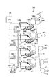
図2は、画像形成部の一つをより詳しく示す。尚、本実施例では、各色用の画像形成部は、形成する画像の色が異なる他は、実質的に同一の構成を有するので、以下、特に区別を要しない場合は、各色用の画像形成部に属する要素であることを示す添え字Y、M、C、Bkを省略して総括的に説明する。 FIG. 2 shows one of the image forming units in more detail. In the present embodiment, the image forming section for each color has substantially the same configuration except that the color of the image to be formed is different. The subscripts Y, M, C, and Bk indicating that the element belongs to the section are omitted, and the description will be made comprehensively.
各画像形成部は、それぞれ像担持体としてのドラム型の電子写真感光体(感光ドラム)10を備えている。感光ドラム10の表面は、感光ドラム10に従動して回転する帯電手段としての帯電ローラ11によって一様に帯電される。次いで、露光手段としての露光装置12が画像信号情報に応じて光信号Lにより走査露光することによって、感光ドラム10の表面に静電潜像が形成される。この静電潜像には、次いで現像手段としての現像装置13によって現像剤としてのトナーが付着され、現像剤像(トナー像)として可視像化される。
Each image forming unit includes a drum-type electrophotographic photosensitive member (photosensitive drum) 10 as an image carrier. The surface of the
例えば、フルカラー画像形成モード時には、各画像形成部において感光ドラム10上に形成された各色のトナー像は、1次転写手段としての1次転写ローラ26に所定の1次転写バイアスが印加されることで、それぞれの画像形成部において感光ドラム10と1次転写ローラ26とが対向する1次転写部N1において、順次中間転写ベルト31上に多重転写される。こうして、中間転写ベルト31上にフルカラー画像が形成される。
For example, in the full-color image forming mode, a predetermined primary transfer bias is applied to a
次いで、2次転写手段としての2次転写ローラ32に所定の2次転写バイアスが印加されることで、中間転写ベルト31上のトナー像は、転写材Sへ2次転写される。転写材Sは、中間転写ベルト31上への画像形成に同期して、転写材カセット41、搬送手段としての転写材供給ローラ42などを備える転写材供給部40から、中間転写ベルト31と2次転写ローラ32とが対向する2次転写部N2に供給される。
Next, a predetermined secondary transfer bias is applied to a
その後、トナー像が転写された記録材Sは定着装置30に搬送されて、転写材Sへの未定着画像の定着が行われる。そして、画像が定着された転写材Sは、排紙トレイ35に搬出されて画像形成は終了する。
Thereafter, the recording material S to which the toner image has been transferred is conveyed to the fixing
又、1次転写時に転写されずに感光ドラム10上に残った1次転写残トナーは、クリーニング部材であるクリーニングブレード14a、廃トナー容器14bを有する像担持体クリーニング手段としてのクリーニング装置14によって、廃トナー容器14bに回収され、感光ドラム10上はクリーニングされる。一方、2次転写時に転写されずに中間転写ベルト31上に残った2次転写残トナーは、中間転写ベルト31に対して離接可能に配設された、中間転写体クリーニング手段(図示せず)によって掻き取られ、中間転写ベルト31上はクリーニングされる。
Further, the primary transfer residual toner that is not transferred during the primary transfer and remains on the
本実施例では、感光ドラム10は直径30mmであり、周速度100mm/secで図中矢印方向に回転駆動される。この感光ドラム1表面は帯電ローラ11により一様に帯電される。
In this embodiment, the
帯電ローラ11には、高圧電源である帯電バイアス電源(図示せず)より−1150Vの直流電圧が印加され、感光ドラム10の表面は、約−600Vの暗部電位で一様に帯電される。本実施例では、帯電バイアスとして、直流バイアスを用いたが、帯電バイアスとして、直流成分に交流成分を重畳したバイアスを用いてもよい。
A DC voltage of −1150 V is applied to the charging
露光装置12は、画像形成装置に入力された画像データに応じて、ON/OFF制御されたレーザーにより感光ドラム10の表面を走査露光し、感光ドラム1の表面に明部電位約−80Vとなる静電潜像を形成する。
The
現像装置13は、図8に示して前述したものと概略同様の構成であり、接触現像方式により、感光ドラム10上の静電潜像を、感光ドラム10の帯電極性と同帯電極性(本実施例では負極性)のトナーを用いて反転現像する。
The developing
更に説明すると、現像装置13は、図2に示すように、現像剤として1成分現像剤である負帯電性の非磁性トナー(1成分トナー)を収容した現像容器(現像装置本体)20に、現像剤担持体としての現像ローラ16、現像剤規制部材としての現像ブレード17、現像剤供給部材としてのトナー供給ローラ18及び現像剤撹拌搬送手段としての攪拌羽根19を備えて構成されている。
More specifically, as shown in FIG. 2, the developing
本実施例では、現像ローラ16は、アルミニウム、アルミニウム合金などの金属からなる芯金16aに、基層16b1とその上の表層16b2とからなる弾性層16bを設けて構成されており、外径16mmである。この弾性層16bの基層16b1は、シリコンなどのゴムからなり、表層16b2はエーテルウレタンやナイロンなどからなっている。勿論、これらに限定されるものではなく、基層16b1にスポンジなどの発泡体を用い、表層16b2にゴム弾性層を形成した構造も可能である。又、抵抗値はφ30の金属円筒に対し、現像ローラ16を総圧1kg加重し、50V印加したときに、1MΩであった。又、本実施例では、現像ローラ16は、周速度160mm/secで駆動手段(図示せず)により回転駆動される。
In this embodiment, the developing
感光ドラム10に形成された静電潜像は、現像時に、感光ドラム10の表面に接触している現像ローラ16に担持されたトナーによって、その接触部(現像部)において可視像化されトナー像とされる。この時、現像ローラ16には、現像電圧印加手段としての高圧電源(現像バイアス電源)23Y、23M、23C、23Bkから−350Vの直流電圧が印加され、負極性に帯電したトナーが、現像ローラ16から感光ドラム1上に形成された静電潜像に転移される。現像バイアスとして、直流成分に交流成分を重畳したバイアスを用いてもよい。
The electrostatic latent image formed on the
このように、インライン方式では、4つの現像装置13が存在し、各色の画像濃度を調整するため、それぞれの現像装置13に対して各々現像バイアス電源23Y、23M、23C、23Bkを配置している。各々現像バイアス電源23Y、23M、23C、23Bkは、その出力電圧をそれぞれ独立して制御(変化)可能となっている。なお、各色の画像濃度を調整するために、例えば、各色毎に参照パッチ画像を形成し、これらの画像濃度を濃度検知手段である濃度センサによって検知し、検知結果に応じて各々現像バイアス電源23Y、23M、23C、23Bkの出力電圧を制御すればよい。即ち、各色の参照パッチ画像の濃度の検知結果に応じて各色の現像ローラ16に印加する現像バイアス電圧を制御すればよい。参照パッチ画像は、中間転写ベルト31上に形成して濃度センサで検知するようにしても、各感光ドラム10上に形成して濃度センサで検知するようにしても良い。
As described above, in the in-line method, there are four developing
現像ローラ16の上方において、現像剤規制部材としての現像ブレード17が現像容器20に支持されている。現像ブレード17は、その自由端側の先端近傍を現像ローラ16の外周面に面接触状態で当接するように設けられている。
Above the developing
本実施例では、現像ブレード17の当接方向は、当接部に対して先端側が現像ローラ16の回転方向上流側に位置する、所謂、カウンタ方向である。又、本実施例では、現像ブレード17は、バネ弾性を有する厚さ0.1mmのリン青銅板を、現像ローラ16の表面に対して所定の線圧で当接している。この現像ブレード17により、現像ローラ16に対する現像ブレード17の圧接力を維持し、摩擦帯電させることで、負帯電性のトナー10に対する帯電性を持たせるとともに現像ローラ16上のトナーの量を規制する。
In this embodiment, the contact direction of the developing
又、現像ブレード17に、規制部材電圧印加手段としての高圧電源(ブレードバイアス電源)から−600Vの直流電圧を印加することで、トナーのコート量を安定化させている。このブレードバイアス電源22は、1つの共通電源で、イエロー、マゼンタ、シアン、ブラックの4色の画像形成部PY、PM、PC、PBkにおける現像装置13Y、13M、13C、13Bkの現像ローラ16に対して、共通して同一のバイアス値(共通電圧)を印加している。
Further, the toner coating amount is stabilized by applying a DC voltage of −600 V to the developing
トナー供給ローラ18は、スポンジ構造や芯金上にレーヨン、ナイロンなどの繊維を植毛したファーブラシ構造とすることができる。但し、現像ローラ16に対するトナーの供給及び現像に供されずに現像ローラ16上に残ったトナーの剥ぎ取りの点から、本実施例では、芯金18a上にウレタンフォーム18bを設けた直径16mmの弾性ローラを用いた。
The
この弾性ローラからなるトナー供給ローラ18は、現像ローラ16に当接して、現像工程時においては、現像ローラ16との当接部において現像ローラ16と反対方向となるようにに周速度100mm/secで回転駆動される。又、トナー供給ローラ18の現像ローラ16に対する侵入量は1.5mmとした。
The
上述のように、感光ドラム10の表面のトナー像は、1次転写電圧印加手段としての1次転写バイアス電源(図示せず)から1次転写バイアスが印加された転写ローラ26により、中間転写ベルト31に転写され、その後、2次転写電圧印加手段としての2次転写バイアス電源(図示せず)から2次転写バイアスが印加された2次転写ローラ32により、転写材Sに転写され、次いで定着される。
As described above, the toner image on the surface of the
引き続き、次なる画像データが画像形成装置100に入力された場合、感光ドラム10、現像ローラ16、トナー供給ローラ18などの回転を停止させることなく、且つ、現像ローラ16は同電位のまま、次なる画像形成動作を繰り返す。
Subsequently, when the next image data is input to the
本実施例においては、現像装置13とともに、回転駆動される感光ドラム10、感光ドラム10の表面を一様に帯電させる帯電ローラ11、及びクリーニング装置14を枠体によって一体的にまとめてプロセスカートリッジ1を構成する。各色用のプロセスカートリッジ1Y、1M、1C、1Bkは、画像形成装置本体2が備える装着手段50を介して、画像形成装置本体2に対し着脱自在である。本実施例では、感光ドラム10、帯電ローラ11、クリーニングブレード17を支持する廃トナー容器14bと、現像ローラ16、現像ブレード17、トナー供給ローラ18、撹拌羽根19を支持する現像容器20を一体的に接続することによってプロセスカートリッジ1を構成している。
In the present embodiment, together with the developing
但し、プロセスカートリッジ1の態様はこれに限定されるものではなく、例えば、現像装置13のみを画像形成装置本体2に固定設置したタイプとすることもできる。つまり、プロセスカートリッジは、像担持体としての感光体と、感光体を帯電させる帯電手段、感光体に現像剤を供給する現像手段、感光体をクリーニングするクリーニング手段のうち少なくとも1つと、を一体的にカートリッジ化し、このカートリッジを画像形成装置本体に対して着脱可能にしたものであればよい。一方、現像装置13のみを、画像形成装置本体2に対して着脱可能なカートリッジ(現像カートリッジ)とすることもできる。
However, the aspect of the
本実施例では、プロセスカートリッジ1が画像形成装置本体2に装着された状態で、画像形成装置本体2に設けられた駆動手段(図示せず)とプロセスカートリッジ1側の駆動伝達手段が接続され、感光ドラム10、現像装置13、帯電ローラ11などが駆動可能な状態となる。更に、プロセスカートリッジ1が画像形成装置本体2に装着された状態で、帯電ローラ11、現像ローラ16、現像ブレード17などに電圧を印加する電源は、プロセスカートリッジ1側及び画像形成装置本体2側にそれぞれ設けられた接点を介して対象と電気的に接続される。
In this embodiment, in a state where the
又、本実施例では、画像形成装置100が備える電源(ブレードバイアス電源、現像バイアス電源、1次転写バイアス電源、2次転写バイアス電源、帯電バイアス電源)は、画像形成装置本体2が有する、装置動作を統括制御する制御手段としてのCPU60(図3)によって制御される。又、本実施例では、制御手段としてのCPU60が、以下説明するように、記憶手段、例えばCPU60の記憶部に予め設定された値に基づき所定タイミングで現像バイアス電源23を制御して、現像バイアスを選択し、切り換える手段として機能する。
In this embodiment, the image forming apparatus main body 2 includes power supplies (blade bias power supply, development bias power supply, primary transfer bias power supply, secondary transfer bias power supply, and charging bias power supply) included in the
次に、フルカラープリントモードとモノクロプリントモードの切り替えについて説明する。 Next, switching between the full color print mode and the monochrome print mode will be described.
本実施例の画像形成装置は、全ての画像形成部を用いてフルカラーの画像を形成するフルカラープリントモード(第1モード)と、特定の色としてブラック単色の画像形成を行う単色画像形成モード(モノクロプリントモード,第2モード)とを有する。 The image forming apparatus according to the present exemplary embodiment includes a full-color print mode (first mode) that forms a full-color image using all the image forming units, and a single-color image formation mode (monochrome) that forms a single black image as a specific color. Print mode, second mode).
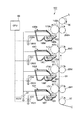
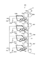
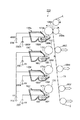
図3及び4は、感光ドラム10、現像装置13、1次転写ローラ26、中間転写ベルト31などを特に示す要部構成図であり、他の要素は省略してある。
FIGS. 3 and 4 are main part configuration diagrams showing the
図3に示すように、中間転写ベルト31は、駆動ローラ36と切り替えローラ37との間に張架されている。切り替えローラ37は、移動手段(図示せず)によって、図中最下位のイエロー用の現像装置13Yに対して近づく方向/遠ざかる方向に移動可能になっている。
As shown in FIG. 3, the
図3は、フルカラープリントモード時の状態を示す。このモードでは、切り替えローラ37は、図中最下位のイエロー用の現像装置13Yに近接する。すると、4つの1次転写ローラ26Y、26M、26C、26Bkはすべて、中間転写ベルト31を介して、対応する感光ドラム10Y、10M、10C、10Bkに当接する。又、4色全ての画像形成部PY、PM、PC、PBkにおいて、感光ドラム10、現像ローラ16、トナー供給ローラ18、及び1次転写ローラ26は、図中矢示の方向に回転駆動されている。
FIG. 3 shows a state in the full color print mode. In this mode, the switching
一方、図4はモノクロプリントモード時の状態を示す。このモードでは、切り替えローラ37は、図中最下位のイエロー用の現像装置13Yから遠ざかる方向(図中矢印方向)に離れる。すると、イエロー、マゼンタ、シアン用の1次転写ローラ26Y、26M、26Cが感光ドラム10Y、10M、10Cから離れるので、これら3色の画像形成部PY、PM、PCにおいては、中間転写ベルト31は感光ドラム10と当接しなくなる。又、この3色の画像形成部PY、PM、PCにおいて、感光ドラム10、現像ローラ16、トナー供給ローラ18、及び1次転写ローラ26は停止される。画像形成を行なわない画像形成部において、感光ドラム10、現像ローラ16、トナー供給ローラ18、及び1次転写ローラ26を使用しないことにより、これらの部材の劣化を防止することができる。また、現像ローラ16とトナー供給ローラ18とを停止することにより、トナーの劣化も防止できる。
On the other hand, FIG. 4 shows a state in the monochrome print mode. In this mode, the switching
本実施例では、制御手段としてのCPU60が、切り替えローラ37の移動、画像形成部の感光ドラム10、現像ローラ16、トナー供給ローラ18、及び1次転写ローラ26の駆動/停止を切り換える切り替え手段としての機能を有する。CPU60は、所定のタイミングで切り替えローラ37の移動手段のON/OFF、一部の画像形成部における感光ドラム10、現像ローラ16、トナー供給ローラ18、及び1次転写ローラ26の駆動手段のON/OFF若しくはクラッチなどの駆動伝達手段のON/OFFなどを、それ自体当業者には容易に理解される一般的な方法によって制御し、上記切り替えを実行させる。
In this embodiment, the
ここで、図10に示すような比較例においては、モノクロプリントモードにおいては、規制部材電圧印加手段として、イエロー、マゼンタ、シアンの画像形成部PY、PM、PCにおける現像ブレード17Y、17M、17Cにブレードバイアスを印加する第1ブレードバイアス電源22aと、ブラックの画像形成部PBkにおける現像ブレード17Bkにブレードバイアスを印加する第2ブレードバイアス電源22bとが設けられていた。そして、モノクロプリントモードにおいては、イエロー、マゼンタ、シアンの3色の画像形成部PY、PM、PCでは、現像ローラ16及び現像ブレード17用の両方の電源を停止していた。
Here, in the comparative example as shown in FIG. 10, in the monochrome print mode, as the regulating member voltage application means, the developing
このように、現像ローラ16と現像ブレード17の両者の電源を0Vに落とせば、前述したような、停止中の現像ローラ16にはトナーの固着は発生しない。
As described above, when both the developing
しかし、図10に示すように、第1ブレードバイアス電源22aと第2ブレードバイアス電源22bとを設けることは、前述のように、電装基板の大型化、コストの増大などの短所がある。
However, as shown in FIG. 10, the provision of the first blade
斯かる観点から、本実施例では、ブレードバイアス電源22を4色の画像形成部に対して共通として、装置小型化、低コスト化を実現している。しかし、このようにブレードバイアス電源22を単一とした場合、モノクロプリントモードにおいてイエロー、マゼンタ、シアンの各画像形成部PY、PM、PCにおいて現像ローラ16が停止されたときに、現像ブレード17と現像ローラ16の両方にバイアスが印加された状態となる。
From this point of view, in this embodiment, the blade
つまり、全ての画像形成部で現像ブレード17用の電源が1つである場合、モノクロプリントモードにおいてイエロー、マゼンタ、シアンの3色の画像形成部PY、PM、PCにおいて現像ローラ16が停止しているにも拘わらず、現像ブレード17にバイアスが印加されてしまう。
That is, when all the image forming units have a single power supply for the developing
よって、現像ブレード17と現像ローラ16にはさまれたトナーは、停止中の現像ローラ16上で常にニップ内に留まり、通電劣化し、ブレードに固着する虞がある。
Therefore, the toner sandwiched between the developing
より具体的には、モノクロプリントモードにおいては、ブラックの画像形成部PBkの現像ブレード17Bkに対し−600Vのバイアスを印加するのが良い。これにより、現像ブレード17Bkの電位をトナーと同極性側に大きくし、トナーを現像ローラ16Bkに向かわせる。しかし、このまま残り3色(イエロー、マゼンタ、シアン)の画像形成部PY、PM、PCの現像ローラ16Y、16M、16Cに印加する現像バイアスを0Vに落としてしまうと、現像ローラ16Y、16M、16Cと、現像ブレード17Y、17M、17Cとの間で600V電位差が発生し、これら現像ローラ16Y、16M、16Cと現像ブレード17Y、17M、17Cとの間に挟まったトナーが通電劣化してしまう。
More specifically, in the monochrome print mode, it is preferable to apply a bias of −600 V to the developing blade 17Bk of the black image forming unit PBk. As a result, the potential of the developing blade 17Bk is increased to the same polarity as the toner, and the toner is directed toward the developing roller 16Bk. However, if the developing bias applied to the developing
そこで、本実施例では、本発明に従って、稼働を止めた現像装置13Y、13M、13Cにおける、現像ブレード17に印加するバイアスと現像ローラ16に印加するバイアスとの電位差が、稼働している特定の現像装置13Bkにおける、現像ブレード17に印加するバイアスと現像ローラ16に印加するバイアスとの差よりも、小さくなるように設定する。即ち、本実施例にて第2の現像剤担持体たる回転を行なわない現像ローラ16Y、16M、16Cと現像ブレード17Y、17M、17Cとの電位差を、本実施例にて第1の現像剤担持体たる回転を行なう現像ローラ16Bkと現像ブレード17Bkとの電位差よりも小さく設定するように、回転を行なわない現像ローラ16Y、16M、16Cに印加される電圧を制御する。
Therefore, in the present embodiment, the potential difference between the bias applied to the developing
本実施例では、イエロー、マゼンタ、シアンの3色の画像形成部PY、PM、PCにおいては、現像ローラ16Y、16M、16Cに印加するバイアスを、画像形成時の−350V(第1バイアス)からさらに強め、−600V(第2バイアス)に変更する。
In this embodiment, in the three color image forming portions PY, PM, and PC of yellow, magenta, and cyan, the bias applied to the developing
フルカラープリントモードとモノクロプリントモードにおける、ブラックの画像形成部PBkと、他の3色(イエロー、マゼンタ、シアン)の画像形成部PY、PM、PCとにおける現像ローラ16、現像ブレード17に印加するバイアス値を表1と表2にまとめる。表1は本実施例であり、表2は比較例を示す。
Bias applied to the developing

以上のように、モノクロプリントモードにおいて、使用していない3色(イエロー、マゼンタ、シアン)の現像ローラ16Y、16M、16Cに印加するバイアスを−600Vにすることにより、現像ブレード17Y、17M、17Cに印加するブレードバイアスの−600Vと等しくする。
As described above, in the monochrome print mode, the developing
これにより、現像ブレード17と現像ローラ16と間の電位差がなくなり、通電しなくなるので、トナーが劣化せず、現像ローラ16と現像ブレード17とのニップ内でのトナー固着を防止することができる。
As a result, the potential difference between the developing
本発明者らの鋭意検討により、モノクロプリントモード時に停止している現像装置3において、現像ブレード17に印加するバイアスと現像ローラ16に印加するバイアスとの差は、300V以上になると、トナーの固着が発生する場合があることが分かった。以下、更に説明する。
As a result of intensive studies by the present inventors, in the developing
試験は、このバイアス差以外は同一である本実施例の画像形成装置100を用いて、現像ブレード17のトナー固着を観察し、画像出力することにより評価し、固着が全くなく、画像にスジがない場合を良好(○)、細かく固着しているものの、スジ画像が出ない場合をやや不良(△)、固着して、スジ画像が発生した場合を不良(×)とした。又、試験は、3色の画像形成部PY、PM、PCの停止時間(現像ローラ16と現像ブレード17との間の通電時間)を30分、60分、90分と変化させて行い、その結果を表3、表4及び表5にそれぞれ示す。
The test was performed by observing toner fixation of the developing
上記表3〜表5の結果から分かるように、現像ローラ16を停止したまま現像ローラ16と現像ブレード17との間に通電すると、通電時間が長いほうがトナー固着が悪化する傾向にある。
As can be seen from the results of Tables 3 to 5, when the developing
従って、60分程度のモノクロ連続プリントを想定すると、現像ローラ16と現像ブレード17との電位差は300V以下にすることが望ましい。又、90分程度のモノクロ連続プリントを想定すると、この電位差は200V以下にすることがより好ましいことが分かる。又、この電位差は、無ければない程よく、本実施例のように0Vであってもよい。
Therefore, assuming monochrome continuous printing of about 60 minutes, it is desirable that the potential difference between the developing
このように、本実施例によれば、モノクロプリント時に、稼働せずに現像ローラ16が停止している現像装置13において、現像ローラ16と現像ブレード17との間の電位差が少なくなるので、現像ローラ16と現像ブレード17との間のニップに挟まれたトナーが現像ブレード17に固着しなくなり、現像スジを防止することができる。しかも、モノクロプリントにおいて稼働していない現像装置13の現像ブレード17にもバイアスを印加することができるので、複数の現像装置13があるにも拘わらず現像ブレード17の高圧電源を1つにすることができる。
As described above, according to the present embodiment, the potential difference between the developing
ここで、停止中の現像ローラ16に−600Vのバイアスを印加すると、停止中の感光ドラム10と現像ローラ16とのニップにおいて、直線状にトナーが感光ドラム10へ引き寄せられている。よって、このまま感光ドラム10を回転させると、感光ドラム10が長手方向に直線状にトナーで現像されてしまう。このようにして感光ドラム10上に移動したトナー量が多いと、中間転写ベルト31を介して転写材Sを汚す虞がある。
Here, when a bias of −600 V is applied to the stopped developing
そこで、本実施例では、モノクロプリントモードからフルカラープリントモードに戻る前に、停止していた現像装置13の現像ローラ16に印加するバイアスを、現像ローラ16にトナーを戻すバイアスに切り換える。つまり、複数の現像装置13の内、一部稼働を止めていた現像装置13を稼働させるときに、当該稼働を止めていた現像装置13の現像ブレードに印加するバイアスを、トナーと逆極性方向に一旦近づけた後、稼働時(画像形成時)のバイアスにする。このシーケンスを図5に示す。
Therefore, in the present embodiment, before returning from the monochrome print mode to the full color print mode, the bias applied to the developing
本実施例では、モノクロプリントモードにおいて、停止中の現像装置13Y、13M、13Cの現像ローラ16と現像ブレード17とには−600Vのバイアスを印加しているが、モノクロプリントモードからフルカラープリントモードに戻る前に、一旦、+100Vのバイアス(第3バイアス)を印加する。このバイアスにより、トナーは現像ローラ16に引き寄せられるので、直線状に感光ドラム10に移動されるトナーを軽減することができた。
In this embodiment, in the monochrome print mode, a bias of −600 V is applied to the developing
尚、感光ドラム10の表面電位は、−600Vから徐々に暗減衰し、最終的に0Vに収束する。従って、0Vよりプラス側であれば、このバイアスはトナーを感光ドラム10から相対的に現像ローラ16側に引き寄せることができる。限定されるものではないが、トナーを現像ローラ16により良く引き寄せるためには、現像ローラ16と感光ドラム10との電位差は、好ましくは0V〜200V、より好ましくは100V〜200Vとする。
Note that the surface potential of the
その後、フルカラープリントモードにおいては、再び、現像ローラ16に印加するバイアスは、−350Vとし、プリント動作を行った。
Thereafter, in the full color print mode, the bias applied to the developing
以上、本実施例のバイアス制御を行うことで、例えば、特定の色の単色画像形成を行うために、他の色の画像形成部の動作を停止する場合に、当該特定色と他の色の画像形成部に対してそれぞれブレードバイアス電源を設けるなど、余分の高圧電源を設けることなく、当該他の色の画像形成部における現像ブレード17へのトナーの固着を防止し、現像スジを防止することができる。
As described above, by performing the bias control of the present embodiment, for example, when the operation of the image forming unit of another color is stopped in order to form a single color image of a specific color, the specific color and the other color Providing a blade bias power source for each image forming unit, etc., without providing an extra high voltage power source, preventing the toner from sticking to the developing
又、停止していた現像装置13を再び駆動させる際に、一旦、トナーが現像ローラ16に向かうバイアスを印加することによって、感光ドラム10に直線状に現像されるトナーを軽減し、中間転写ベルト31を介して転写材Sの裏汚れが発生する危険性をも排除することができる。
Further, when the developing
実施例2
次に、本発明の他の実施例について説明する。本実施例の画像形成装置の基本構成、動作は実施例1のものと同じであるので、同一構成、作用を有する要素には同一符号を付し、詳しい説明は省略する。
Example 2
Next, another embodiment of the present invention will be described. Since the basic configuration and operation of the image forming apparatus of the present embodiment are the same as those of the first embodiment, elements having the same configuration and function are denoted by the same reference numerals, and detailed description thereof is omitted.
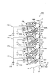
図6は、本実施例の画像形成装置の感光ドラム10、現像装置13、1次転写ローラ26、中間転写ベルト31を特に示す要部概略構成図であり、モノクロプリントモード時の状態を示す。図示の通り、実施例1と同様、モノクロモードにおいては、イエロー、マゼンタ、シアンの各画像形成部PY、PM、PCにおいて、感光ドラム10、現像ローラ16、トナー供給ローラ17、1次転写ローラ26は停止している。そして、このとき、これら3色の画像形成部PY、PM、PCにおいて、実施例1と同様に、現像ブレード17及び現像ローラ16の両方にバイアスが印加さる。
FIG. 6 is a schematic configuration diagram of a principal part particularly showing the
つまり、本実施例の画像形成装置では、実施例1と同様、現像ブレード17用の電源を1つだけ設けることで、装置の小型化、低コスト化を実現している。このため、停止中の3色(イエロー、マゼンタ、シアン)の画像形成部PY、PM、PCにおいては、現像ローラ16Y、16M、16Cが停止しているにも拘わらず、現像ブレード17Y、17M、17Cにブレードバイアスが印加されることになる。
That is, in the image forming apparatus according to the present embodiment, as in the first embodiment, only one power source for the developing
より具体的には、モノクロプリントモードにおいては、ブラックの画像形成部PBkの現像ブレード17Bkに対し−600Vのバイアスを印加する必要がある。しかし、このまま残り3色(イエロー、マゼンタ、シアン)の画像形成部PY、PM、PCの現像ローラ16Y、16M、16Cに印加するバイアスを0Vに落としてしまうと、現像ローラ16Y、16M、16Cと、現像ブレード17Y、17M、17Cとの間で600Vの電位差が発生し、これら現像ローラ16Y、16M、16Cと現像ブレード17Y、17M、17Cとの間に挟まったトナーが通電劣化してしまう。
More specifically, in the monochrome print mode, it is necessary to apply a bias of −600 V to the developing blade 17Bk of the black image forming unit PBk. However, if the bias applied to the developing
そこで、これら停止中の3色(イエロー、マゼンタ、シアン)の画像形成部PY、PM、PCにおいて、現像ローラ16に印加するバイアスを画像形成時の−350V(第1バイアス)からさらに強め、−600V(第バイアス)に変更する。
Therefore, in the stopped three color (yellow, magenta, cyan) image forming portions PY, PM, and PC, the bias applied to the developing
一方、実施例1にて説明したように、停止中の現像ローラ16に−600Vのバイアスを印加するので、現像ローラ16が感光ドラム10と接触していると、停止中の感光ドラム10とのニップにおいて、直線状にトナーが感光ドラム10へ引き寄せられて、感光ドラム10が直線状に現像されてしまう。
On the other hand, since the bias of −600 V is applied to the stopped developing
そこで、本実施例では、図6に示すように、モノクロプリントモードでは、以下に説明するシーケンスに従って、イエロー、マゼンタ、シアンの画像形成部PY、PM、PCにおいて現像ローラ16Y、16M、16Cを、図中矢印にて示すように、感光ドラム10から離間させる。
Therefore, in this embodiment, as shown in FIG. 6, in the monochrome print mode, the developing
斯かる離間動作のシーケンスを図7に示す。イエロー、マゼンタ、シアンの画像形成部PY、PM、PCにおける停止中の現像ローラ16と現像ブレード17とには、−600Vのバイアスを印加するが、この直前に、これら3色の画像形成部PY、PM、PCにおける現像ローラ16を感光ドラム10から離間させる。その後、モノクロプリントモードからフルカラープリントに戻るときは、現像ローラ16に印加するバイアスを−350Vに戻した後、現像ローラ16を感光ドラム10に当接させる。このとき、感光ドラム10の表面電位は、所定の−600Vに保たれているので、感光ドラム10上にトナーが移動することなない。
FIG. 7 shows a sequence of such a separation operation. A bias of −600 V is applied to the developing
これによって、感光ドラム10に直線上に現像されることがなく、転写材の裏汚れ防止が可能となる。
As a result, the
現像ローラ16を感光ドラム10から離間させるには、例えば感光ドラム10を支持する廃トナー容器14bに揺動可能に接合されて一体的にプロセスカートリッジ1を構成する現像容器20を、画像形成装置本体2に設けられた駆動手段(図示せず)によって往復移動される離間手段70によって、揺動軸71を中心にして揺動させる。本実施例では、この離間手段70の動作は、制御手段としてのCPU60が制御する。但し、本発明は、現像ローラ16の離間手段をこれに限定するものではなく、同一の目的のために、当業者は考えられる如何なる離間手段をも採用することができる。斯かる変更は、本発明の設計変更の範囲内にある。
In order to separate the developing
以上の離間当接動作を行うことで、停止中に現像ブレード17に印加するブレードバイアスと同じ電位のバイアスを現像ローラ16に印加しても、感光ドラム10へ直線状にトナーが移動することがなくなり、中間転写ベルト31を介しての転写材Sの裏汚れを防止することができた。
By performing the above-described separation contact operation, the toner moves linearly to the
以上、本実施例によれば、実施例1同様、例えば、特定の色の単色画像形成を行うために、他の色の画像形成部の動作を停止する場合に、当該特定色と他の色の画像形成部に対してそれぞれブレードバイアス電源を設けるなど、余分の高圧電源を設けることなく、当該他の色の画像形成部における現像ブレード17へのトナーの固着を防止、現像スジを防止することができる。
As described above, according to the present embodiment, as in the first embodiment, for example, when the operation of the image forming unit of another color is stopped in order to form a single color image of a specific color, the specific color and the other color Without providing an extra high voltage power source such as providing a blade bias power source for each of the image forming units, toner sticking to the developing
又、上述のように停止する画像形成部における現像ローラ16を感光ドラム10に対して離間/当接させることによって、感光ドラム10上をトナーで直線状に現像することもなく、中間転写ベルト31を介して転写材Sの裏汚れが発生する危険性をも排除することができる。
Further, by causing the developing
尚、上記各実施例においては、画像形成装置は中間転写方式であるとして説明したが、当業者には周知のように、中間転写体の代わりに転写材担持体を有し、この転写材担持体上に担持して各画像形成部に搬送される転写材上に、各画像形成部から順次トナー像を重ねて転写した後、この転写材を転写材担持体から分離して未定着トナー像を定着し、例えばフルカラー画像を得る画像形成装置がある。本発明はこのような画像形成装置にも等しく適用可能である。 In each of the above embodiments, the image forming apparatus is described as an intermediate transfer system. However, as is well known to those skilled in the art, a transfer material carrier is provided instead of the intermediate transfer body, and this transfer material carrier is used. After transferring the toner images from the respective image forming units on the transfer material carried on the body and transported to the respective image forming units, the transfer material is separated from the transfer material carrying member and transferred to the unfixed toner image. For example, there is an image forming apparatus that obtains a full color image. The present invention is equally applicable to such an image forming apparatus.
又、像担持体としては、感光ドラム以外にも感光ベルトを用いることもでき、更には、感光体でなく誘電体も使用することができる。誘電体には、電荷を直接付与するイオンヘッドによって静電潜像を形成すればよい。 In addition to the photosensitive drum, a photosensitive belt can be used as the image carrier, and further, a dielectric can be used instead of the photosensitive member. An electrostatic latent image may be formed on the dielectric by an ion head that directly applies charges.
1 プロセスカートリッジ
2 画像形成装置本体
10 感光ドラム(像担持体)
11 帯電ローラ(帯電手段)
12 露光装置(露光手段)
13 現像装置(現像手段)
16 現像ローラ(現像剤担持体)
17 現像ブレード(現像剤規制部材)
18 トナー供給ローラ(現像剤供給部材)
22 ブレードバイアス電源(規制部材電圧印加手段)
23 現像バイアス電源(現像電圧印加手段)
26 1次転写ローラ(1次転写手段)
36 駆動ローラ
37 切り替えローラ
31 中間転写ベルト(中間転写体)
60 制御手段
70 離間手段
DESCRIPTION OF
11 Charging roller (charging means)
12 Exposure equipment (exposure means)
13 Developing device (Developing means)
16 Development roller (developer carrier)
17 Development blade (developer regulating member)
18 Toner supply roller (developer supply member)
22 Blade bias power supply (regulator member voltage application means)
23 Development bias power supply (development voltage application means)
26 Primary transfer roller (primary transfer means)
36
60 Control means 70 Separation means
Claims (12)
前記複数の現像剤規制部材に共通電圧を印加する共通の電圧印加手段と、
を有し、
前記複数の現像剤担持体の全部が回転して画像形成を行なう第1の画像形成モードと、前記複数の現像剤担持体のうち第1の現像剤担持体が回転し、前記複数の現像剤担持体のうち前記第1の現像剤担持体以外の全部の現像剤担持体が回転しないで画像形成を行なう第2の画像形成モードと、を切り替え可能であり、
前記第2の画像形成モードにおいて、前記複数の現像剤担持体のうち前記第1の現像剤担持体以外の全部の現像剤担持体の各電位と前記共通電圧との各電位差は、前記第1の現像剤担持体の電位と前記共通電圧との電位差よりも小さいことを特徴とする画像形成装置。 A developer carrying member that carries and conveys the developer to develop the electrostatic image formed on the image carrying member with the developer, a developer regulating member that regulates the developer carried on the developer carrying member, A plurality of developing devices each comprising:
A common voltage applying means for applying a common voltage to the plurality of developer regulating members;
Have
A first image forming mode in which all of the plurality of developer carriers rotate to form an image; and a first developer carrier of the plurality of developer carriers rotates, and the plurality of developers It is possible to switch between a second image forming mode in which image formation is performed without rotation of all the developer carriers other than the first developer carrier among the carriers,
In the second image forming mode, each potential difference between each potential of all developer carriers other than the first developer carrier and the common voltage among the plurality of developer carriers is the first voltage difference. An image forming apparatus, wherein the potential difference between the potential of the developer carrying member and the common voltage is smaller.
部の現像剤担持体を回転させるときに、前記複数の現像剤担持体のうち前記第1の現像剤担持体以外の全部の現像剤担持体に印加する電圧は、前記複数の現像剤担持体のうち前記第1の現像剤担持体以外の全部の現像剤担持体に現像時の電圧を印加する前に、現像時の電圧よりも現像剤の帯電極性と逆極性方向に近づけた電圧を印加することを特徴とする請求項1〜4のいずれかの項に記載の画像形成装置。 When rotating all the developer carriers other than the first developer carrier among the plurality of developer carriers whose rotation has been stopped, the first of the plurality of developer carriers is rotated. The voltage to be applied to all the developer carriers other than the developer carrier is the voltage at the time of development applied to all the developer carriers other than the first developer carrier among the plurality of developer carriers. before, the image forming apparatus according to any one of claims 1-4 than the voltage at the time of development and applying a voltage close to the charging polarity opposite direction of the developer.
前記複数の現像剤規制部材に共通電圧を印加する共通の電圧印加手段と、
前記複数の現像装置のそれぞれに対応する複数の像担持体と、
を有し、
前記複数の現像剤担持体のそれぞれは、前記複数の像担持体のそれぞれに接触可能であり、前記複数の現像剤担持体のうち第1の現像剤担持体以外の全部の現像剤担持体が現像動作を行なわないとき、前記複数の現像剤担持体のうち前記第1の現像剤担持体以外の全部の現像剤担持体の回転を停止するとともに、前記複数の現像剤担持体のうち前記第1の現像剤担持体以外の全部の現像剤担持体をこれに対応する像担持体から離間させ、前記複数の現像剤担持体のうち前記第1の現像剤担持体以外の全部の現像剤担持体が現像動作を行なうとき、前記複数の現像剤担持体のうち前記第1の現像剤担持体以外の全部の現像剤担持体をこれに対応する像担持体と接触させるよう構成され、
前記複数の現像剤担持体のうち前記第1の現像剤担持体が回転し、前記複数の現像剤担持体のうち前記第1の現像剤担持体以外の全部の現像剤担持体が回転しないとき、前記複数の現像剤担持体のうち前記第1の現像剤担持体以外の全部の現像剤担持体の各電位と前記共通電圧との各電位差は、前記第1の現像剤担持体の電位と前記共通電圧との電位差よりも小さいことを特徴とする画像形成装置。 A developer carrying member that carries and conveys the developer to develop the electrostatic image formed on the image carrying member with the developer, a developer regulating member that regulates the developer carried on the developer carrying member, A plurality of developing devices each comprising:
A common voltage applying means for applying a common voltage to the plurality of developer regulating members ;
A plurality of image carriers corresponding to each of the plurality of developing devices ;
Have
Wherein each of the developer carrying member is contactable to each of the plurality of image bearing members, wherein the plurality of developer carrying member sac Chi first of all but the developer carrying member the developer carrying member When the developing operation is not performed, rotation of all developer carriers other than the first developer carrier among the plurality of developer carriers is stopped, and the developer carrier among the plurality of developer carriers is All developer carriers other than the first developer carrier are separated from the corresponding image carriers, and all the developers other than the first developer carrier among the plurality of developer carriers. When the carrier performs a developing operation, all the developer carriers other than the first developer carrier among the plurality of developer carriers are configured to come into contact with the corresponding image carrier ,
When the first developer carrier among the plurality of developer carriers rotates, and all the developer carriers other than the first developer carrier among the plurality of developer carriers do not rotate. The potential differences between the potentials of all the developer carriers other than the first developer carrier and the common voltage among the plurality of developer carriers are the potential of the first developer carrier. the common voltage and images forming device you being smaller than the potential difference.
前記複数の現像剤規制部材に共通電圧を印加する共通の電圧印加手段と、
前記複数の現像装置のそれぞれに対応する複数の像担持体と、
を有し、
前記複数の現像剤担持体のそれぞれは、前記複数の像担持体のそれぞれに接触可能であり、前記複数の現像剤担持体のうち第1の現像剤担持体以外の全部の現像剤担持体が現像動作を行なわないとき、前記複数の現像剤担持体のうち前記第1の現像剤担持体以外の全部の現像剤担持体の回転を停止するとともに、前記複数の現像剤担持体のうち前記第1の現像剤担持体以外の全部の現像剤担持体をこれに対応する像担持体から離間させ、前記複数の現像剤担持体のうち前記第1の現像剤担持体以外の全部の現像剤担持体が現像動作を行なうとき、前記複数の現像剤担持体のうち前記第1の現像剤担持体以外の全部の現像剤担持体に現像電圧を印加した後で、前記複数の現像剤担持体のうち前記第1の現像剤担持体以外の全部の現像剤担持体をこれに対応する像担持体と接触させるよう構成され、
前記複数の現像剤担持体のうち前記第1の現像剤担持体が回転し、前記複数の現像剤担持体のうち前記第1の現像剤担持体以外の全部の現像剤担持体が回転しないとき、前記複数の現像剤担持体のうち前記第1の現像剤担持体以外の全部の現像剤担持体の各電位と前記共通電圧との各電位差は、前記第1の現像剤担持体の電位と前記共通電圧との電位差よりも小さいことを特徴とする画像形成装置。 A developer carrying member that carries and conveys the developer to develop the electrostatic image formed on the image carrying member with the developer, a developer regulating member that regulates the developer carried on the developer carrying member, A plurality of developing devices each comprising:
A common voltage applying means for applying a common voltage to the plurality of developer regulating members ;
A plurality of image carriers corresponding to each of the plurality of developing devices ;
Have
Wherein each of the developer carrying member is contactable to each of the plurality of image bearing members, wherein the plurality of developer carrying member sac Chi first of all but the developer carrying member the developer carrying member When the developing operation is not performed, rotation of all developer carriers other than the first developer carrier among the plurality of developer carriers is stopped, and the developer carrier among the plurality of developer carriers is All developer carriers other than the first developer carrier are separated from the corresponding image carriers, and all the developers other than the first developer carrier among the plurality of developer carriers. When the carrier performs a developing operation, a developing voltage is applied to all developer carriers other than the first developer carrier among the plurality of developer carriers, and then the plurality of developer carriers. Of all the developer carriers other than the first developer carrier. Configured for contacting with the image bearing member corresponding to Les,
When the first developer carrier among the plurality of developer carriers rotates, and all the developer carriers other than the first developer carrier among the plurality of developer carriers do not rotate. The potential differences between the potentials of all the developer carriers other than the first developer carrier and the common voltage among the plurality of developer carriers are the potential of the first developer carrier. the common voltage and images forming device you being smaller than the potential difference.
Priority Applications (2)
| Application Number | Priority Date | Filing Date | Title |
|---|---|---|---|
| JP2003369718A JP4366173B2 (en) | 2002-11-19 | 2003-10-29 | Image forming apparatus |
| US10/715,533 US7050733B2 (en) | 2002-11-19 | 2003-11-19 | Image forming apparatus including two developer carrying members wherein potential differences between the developer carrying members and a common voltage source differ |
Applications Claiming Priority (2)
| Application Number | Priority Date | Filing Date | Title |
|---|---|---|---|
| JP2002335835 | 2002-11-19 | ||
| JP2003369718A JP4366173B2 (en) | 2002-11-19 | 2003-10-29 | Image forming apparatus |
Publications (3)
| Publication Number | Publication Date |
|---|---|
| JP2004184989A JP2004184989A (en) | 2004-07-02 |
| JP2004184989A5 JP2004184989A5 (en) | 2008-12-18 |
| JP4366173B2 true JP4366173B2 (en) | 2009-11-18 |
Family
ID=32716268
Family Applications (1)
| Application Number | Title | Priority Date | Filing Date |
|---|---|---|---|
| JP2003369718A Expired - Fee Related JP4366173B2 (en) | 2002-11-19 | 2003-10-29 | Image forming apparatus |
Country Status (2)
| Country | Link |
|---|---|
| US (1) | US7050733B2 (en) |
| JP (1) | JP4366173B2 (en) |
Families Citing this family (13)
| Publication number | Priority date | Publication date | Assignee | Title |
|---|---|---|---|---|
| DE102004005964A1 (en) * | 2004-02-06 | 2005-09-08 | OCé PRINTING SYSTEMS GMBH | Control device and method for controlling an electrophotographic printer or copier |
| JP2007058073A (en) * | 2005-08-26 | 2007-03-08 | Brother Ind Ltd | Image forming apparatus |
| JP5089155B2 (en) * | 2006-12-12 | 2012-12-05 | キヤノン株式会社 | Developing device and cartridge |
| JP5207633B2 (en) * | 2007-02-14 | 2013-06-12 | キヤノン株式会社 | Image forming apparatus |
| JP2009163030A (en) * | 2008-01-08 | 2009-07-23 | Sharp Corp | Image forming apparatus and drive control method therefor |
| JP5407243B2 (en) * | 2008-09-16 | 2014-02-05 | 株式会社リコー | Image forming apparatus |
| JP5419657B2 (en) * | 2009-01-30 | 2014-02-19 | キヤノン株式会社 | Image forming apparatus |
| US8285161B2 (en) * | 2009-05-29 | 2012-10-09 | Brother Kogyo Kabushiki Kaisha | Image forming apparatus operable in monochrome and color printing modes |
| JP2011013663A (en) * | 2009-06-01 | 2011-01-20 | Canon Inc | Image forming apparatus |
| JP2011112919A (en) * | 2009-11-27 | 2011-06-09 | Canon Inc | Apparatus and method for forming image |
| JP2015082066A (en) | 2013-10-24 | 2015-04-27 | キヤノン株式会社 | Image forming apparatus |
| JP6270676B2 (en) * | 2014-09-22 | 2018-01-31 | 株式会社沖データ | Image forming apparatus |
| JP7459603B2 (en) * | 2020-03-26 | 2024-04-02 | ブラザー工業株式会社 | Image forming device |
Family Cites Families (11)
| Publication number | Priority date | Publication date | Assignee | Title |
|---|---|---|---|---|
| JPH0493963A (en) * | 1990-08-06 | 1992-03-26 | Ricoh Co Ltd | Developing device |
| US5376998A (en) * | 1991-10-24 | 1994-12-27 | Canon Kabushiki Kaisha | Image formation apparatus including a plurality of development unit selectively driven by a common power source |
| JPH06289703A (en) | 1993-03-31 | 1994-10-18 | Canon Inc | Developing device |
| US5862438A (en) * | 1998-08-06 | 1999-01-19 | Xerox Corporation | Reduced interdocument zone in a printing system having a single developer power supply |
| US6029018A (en) * | 1998-09-10 | 2000-02-22 | Tektronix, Inc. | Color capable electrophotographic printer |
| JP2000098739A (en) * | 1998-09-21 | 2000-04-07 | Minolta Co Ltd | Developing device |
| JP3595698B2 (en) | 1998-09-28 | 2004-12-02 | キヤノン株式会社 | Development density adjustment method |
| JP3768702B2 (en) | 1998-10-16 | 2006-04-19 | キヤノン株式会社 | Developing device and image forming apparatus |
| JP3919381B2 (en) | 1999-05-14 | 2007-05-23 | キヤノン株式会社 | Developing device, developing cartridge, process cartridge, and image forming apparatus |
| JP4124988B2 (en) | 2001-10-15 | 2008-07-23 | キヤノン株式会社 | Image forming apparatus |
| CN1236365C (en) * | 2001-12-28 | 2006-01-11 | 佳能株式会社 | Developing equipment and imaging equipment |
-
2003
- 2003-10-29 JP JP2003369718A patent/JP4366173B2/en not_active Expired - Fee Related
- 2003-11-19 US US10/715,533 patent/US7050733B2/en not_active Expired - Fee Related
Also Published As
| Publication number | Publication date |
|---|---|
| US7050733B2 (en) | 2006-05-23 |
| JP2004184989A (en) | 2004-07-02 |
| US20040136742A1 (en) | 2004-07-15 |
Similar Documents
| Publication | Publication Date | Title |
|---|---|---|
| JP6071497B2 (en) | Image forming apparatus | |
| JP2008191514A (en) | Image forming apparatus | |
| JPS63109457A (en) | Image forming device | |
| JP4366173B2 (en) | Image forming apparatus | |
| US8428477B2 (en) | Image forming apparatus | |
| US7738803B2 (en) | Image forming method and apparatus for effectively charging an image carrier | |
| US7269382B2 (en) | Developing apparatus | |
| JP5518125B2 (en) | Electrophotographic image forming apparatus | |
| JP2008180902A (en) | Image forming device | |
| JP2008191246A (en) | Image forming apparatus | |
| JP2004246146A (en) | Image forming apparatus and cartridge | |
| JP2017107075A (en) | Image forming apparatus | |
| JP2004252420A (en) | Developing device, process cartridge, and image forming apparatus | |
| JP2014112266A (en) | Electrophotographic image forming apparatus | |
| JP2005173228A (en) | Image forming apparatus | |
| JP5950874B2 (en) | Image forming apparatus | |
| JP4289873B2 (en) | Image forming apparatus | |
| JP5839878B2 (en) | Image forming apparatus | |
| JP2007093771A (en) | Image forming apparatus | |
| JP2009086140A (en) | Image forming apparatus | |
| JP2001147572A (en) | Image forming device | |
| JP6278260B2 (en) | Developing device and image forming apparatus having the same | |
| JP2014010340A (en) | Bias control device, developing device, process cartridge and image forming apparatus | |
| JP2005148281A (en) | Image forming apparatus | |
| JP2008070637A (en) | Electrifying device and image forming apparatus |
Legal Events
| Date | Code | Title | Description |
|---|---|---|---|
| A621 | Written request for application examination |
Free format text: JAPANESE INTERMEDIATE CODE: A621 Effective date: 20061020 |
|
| A521 | Request for written amendment filed |
Free format text: JAPANESE INTERMEDIATE CODE: A523 Effective date: 20081031 |
|
| A977 | Report on retrieval |
Free format text: JAPANESE INTERMEDIATE CODE: A971007 Effective date: 20090105 |
|
| A131 | Notification of reasons for refusal |
Free format text: JAPANESE INTERMEDIATE CODE: A131 Effective date: 20090310 |
|
| A521 | Request for written amendment filed |
Free format text: JAPANESE INTERMEDIATE CODE: A523 Effective date: 20090511 |
|
| A131 | Notification of reasons for refusal |
Free format text: JAPANESE INTERMEDIATE CODE: A131 Effective date: 20090602 |
|
| A521 | Request for written amendment filed |
Free format text: JAPANESE INTERMEDIATE CODE: A523 Effective date: 20090713 |
|
| TRDD | Decision of grant or rejection written | ||
| A01 | Written decision to grant a patent or to grant a registration (utility model) |
Free format text: JAPANESE INTERMEDIATE CODE: A01 Effective date: 20090811 |
|
| A01 | Written decision to grant a patent or to grant a registration (utility model) |
Free format text: JAPANESE INTERMEDIATE CODE: A01 |
|
| A61 | First payment of annual fees (during grant procedure) |
Free format text: JAPANESE INTERMEDIATE CODE: A61 Effective date: 20090824 |
|
| FPAY | Renewal fee payment (event date is renewal date of database) |
Free format text: PAYMENT UNTIL: 20120828 Year of fee payment: 3 |
|
| R150 | Certificate of patent or registration of utility model |
Free format text: JAPANESE INTERMEDIATE CODE: R150 |
|
| FPAY | Renewal fee payment (event date is renewal date of database) |
Free format text: PAYMENT UNTIL: 20120828 Year of fee payment: 3 |
|
| FPAY | Renewal fee payment (event date is renewal date of database) |
Free format text: PAYMENT UNTIL: 20130828 Year of fee payment: 4 |
|
| LAPS | Cancellation because of no payment of annual fees |