JP4352944B2 - Optical circuit manufacturing method - Google Patents
Optical circuit manufacturing method Download PDFInfo
- Publication number
- JP4352944B2 JP4352944B2 JP2004065385A JP2004065385A JP4352944B2 JP 4352944 B2 JP4352944 B2 JP 4352944B2 JP 2004065385 A JP2004065385 A JP 2004065385A JP 2004065385 A JP2004065385 A JP 2004065385A JP 4352944 B2 JP4352944 B2 JP 4352944B2
- Authority
- JP
- Japan
- Prior art keywords
- light
- core
- wavelength
- photocurable resin
- refractive index
- Prior art date
- Legal status (The legal status is an assumption and is not a legal conclusion. Google has not performed a legal analysis and makes no representation as to the accuracy of the status listed.)
- Expired - Fee Related
Links
Images


Landscapes
- Optical Integrated Circuits (AREA)
- Optical Modulation, Optical Deflection, Nonlinear Optics, Optical Demodulation, Optical Logic Elements (AREA)
- Lasers (AREA)
Abstract
Description
本発明は、発明者らにより開発された自己形成型の光導波路を用いた光回路に関する。本発明は、小型化可能な光回路に関し、特に光増幅、光分岐、波長分割、ノイズとして混入する所望しない波長光の除去、更には光スイッチ、非線形媒質による強度変調等の機能を有する光回路に関する。本発明によればコンパクトな光回路が作製可能であり、且つ各部品の光軸調整を不要とすることができるので、当該光回路の製造が容易となる。 The present invention relates to an optical circuit using a self-forming optical waveguide developed by the inventors. The present invention relates to an optical circuit that can be miniaturized, and in particular, an optical circuit having functions such as optical amplification, optical branching, wavelength division, removal of undesired wavelength light mixed as noise, optical switching, and intensity modulation by a nonlinear medium. About. According to the present invention, a compact optical circuit can be manufactured, and the optical axis adjustment of each component can be made unnecessary, so that the optical circuit can be easily manufactured.
背景技術について上記5文献により説明する。非特許文献1は、本願の共同出願人の1人による論文である。ドライエッチングなどの真空プロセスを用いて、信号波長に対して透明な光導波路内に非線形光学結晶を埋め込んだチャネル型のカスケード導波路を作製する技術について開示されている。
Background art will be described with reference to the above five documents. Non-Patent
特許文献1は、希土類イオンをドープしたガラス基板上に増幅用光導波路とインターコネクション用の段差を、エッチングとフォトリソグラフィーなどの平面プロセスを用いて形成するものである。段差端部に透明な信号光用導波路を対峙配置させ、この信号光用導波路に光結合可能な平行配置された励起用光導波路からなる構造を開示している。特許文献2は、分波器を用いて、励起光を効率良く信号光と干渉させるために、コリメートレンズとファラデー回転子を用いたレンズ光学系により構成された光増幅器を開示している。
In
特許文献3は、「光デバイスの一部又は全部に蛍光物質、二光子吸収発光物質、アップコンバージョン物質およびSHG物質から選ばれる物質を含有させ、励起光により発光を生じさせる(請求項29)」技術を開示している。当該材料により波長変換された光自身によって材料の屈折率変化を誘起して光導波路を形成するというものである。特許文献4は、本願の共同出願人の1人による先行出願の公開公報であり、光硬化性樹脂液(未硬化樹脂)を用いた、自己形成型の光導波路が開示されている。
非特許文献1に記載された技術では、励起光を効率良く非線形光学結晶に導くために、非線形光学結晶を矩形断面の光導波路に加工し、且つ、この光導波路に励起光を導くための光導波路を同一の矩形断面の光導波路に加工して、接続しなくてはならない。これは、プロセスの点で、精密で煩雑な加工を要求される。異なる複数の機能性導波路の挿入や光学フィルタの挿入と云った多段化を行うためには、高精度の機械加工が要求され、性能、コスト面での実現困難と考えられる。
In the technique described in
特許文献1に記載された技術は、一般的に検討されている方法だが、上記同様、別々に作製された物をフォトリソグラフィー等の技術を用い、精密加工技術を用いて位置合せを行うものであり、高い精度が要求される。複数の機能性材料を集積する場合には、極端に加工が難しくなる上に、導波損失の増加が生じる。また、特許文献2に記載された技術はレンズを用いて励起効率を上げている。大型の光学系は結合効率を高めることは可能であるが、反面、小型化と低コスト化、量産化が困難である。また、振動にも弱いので、自動車や民生機器への適用は難しい。
The technique described in
特許文献3においては、従来例として、蛍光物質、二光子吸収発光物質、アップコンバージョン物質およびSHG物質が挙げられている。これらは導波路を硬化させるために機能する材料であって、実際の通信においては導波損失要因になってしまう。特許文献3では、通信で使用する光源の波長(一般的に赤外光)では材料は硬化しないため、上記材料を添加し、2倍の周波数の光(波長で云うと半分)に変換して硬化を促進しようというものである。つまり、通信波長の光を強く吸収しなければ波長変換が行われないので、実際の通信においても大きな損失要因となる。
In
特許文献4に記載の技術は本発明と密接に関わるものである。コア形成後、未硬化成分を溶剤除去し、コア材料よりも屈折率の低い材料で埋め込むことが開示されている。コア材料及びクラッド材料が1デバイスにつきそれぞれ一種類であり、複数の機能デバイスを作製して連結する場合の方策には言及されていない。
The technique described in
このような技術的背景に立ち、本発明者らは自己形成型の光導波路を有する複合的機能を有する光回路を一体形成可能とする発明を完成させた。本発明の目的は、小型化可能であって光軸調整の実質的に不要な光回路を提供することである。 In view of such a technical background, the present inventors have completed an invention that can integrally form an optical circuit having a composite function having a self-forming optical waveguide. An object of the present invention is to provide an optical circuit that can be miniaturized and that is substantially unnecessary for optical axis adjustment.
請求項1に係る発明は、光硬化性樹脂の硬化物から成る軸状のコアを有し、1個以上のフィルタ素子を有し、各フィルタ素子を挟んで形成されたコアの光軸が一致しており、フィルタ素子の少なくとも1個について、当該フィルタ素子を挟んで両側にコアが形成されており、当該2つのコアの組成又は添加物が異なる、及び/又は、当該2つのコアをそれぞれ取り巻く2つのクラッドの組成又は添加物が異なる光回路を製造する方法についての発明である。即ち、光導波路のコア形成のための樹脂硬化光を導入する窓を有する光回路容器に1個以上のフィルタ素子を配置させ、且つ当該各フィルタ素子を含む隔壁にて光回路容器を2個以上の部屋に区分けし、2個以上の部屋のうち樹脂硬化光を導入する窓を有する部屋を含む2個以上の部屋の各々に、未硬化の光硬化性樹脂を充填し、窓から樹脂硬化光を導入することにより、各部屋の光硬化性樹脂を硬化させて、各フィルタ素子を挟む各コアの光軸が一致するように当該各コアを形成し、各部屋における各コアの周囲に、クラッドを形成し、フィルタ素子の少なくとも1個について、当該フィルタ素子を挟んで両側の部屋に充填される光硬化性樹脂の成分又はその光硬化性樹脂に対する添加物を異ならせることにより、当該フィルタ素子を挟んで両側に形成される2つのコアの組成又は添加物が異なるようにし、及び/又は、当該2つのコアをそれぞれ取り巻く2つのクラッドを構成する材料の組成又はその材料に対する添加物を異ならせることにより、その2つのクラッドの組成又は添加物が異なるようにしたことを特徴とする。
ここでフィルタ素子とは、波長選択性フィルタ、波長選択性ミラー、光シャッターの他、全反射ミラー、更には電場によりそれらの間の光導波路の性質を変化させる2つの電極を含むものとする。また、軸状のコアは、いわゆる3次元構造の光導波路を言うものであって、基板上に平面的に形成されるものを言うものではない。またコアが分岐を含む場合の「光軸が一致」は、各フィルタ素子を挟む2つのコアの光軸を言い、分岐の光軸については問わないものである。
また、ここで「窓」とは、光回路容器の当該窓部分が「空いているか」少なくとも樹脂硬化光及び通信波長に対して透明であることを言う。光回路容器は、必要部分のみ通信波長等に対して透明であれば良い。また、光回路容器には、未硬化の光硬化性樹脂(液)を充填する必要があるので、光回路容器を「密閉」する必要は必ずしも無い。例えば静置した状態で上面が開放状態であっても良い。
The invention according to
Here, the filter element includes a wavelength selective filter, a wavelength selective mirror, an optical shutter, a total reflection mirror, and two electrodes that change the properties of the optical waveguide between them by an electric field. Further, the axial core refers to an optical waveguide having a so-called three-dimensional structure, and does not refer to a planar shape formed on a substrate. The “optical axis coincides” in the case where the core includes a branch means the optical axis of the two cores sandwiching each filter element, and the optical axis of the branch does not matter.
Here, “window” means that the window portion of the optical circuit container is “open” or at least transparent to the resin curing light and the communication wavelength. The optical circuit container only needs to be transparent with respect to the communication wavelength or the like only in necessary portions. In addition, since it is necessary to fill the optical circuit container with an uncured photocurable resin (liquid), it is not always necessary to “seal” the optical circuit container. For example, the upper surface may be in an open state in a stationary state.
請求項2に係る発明は、請求項1に係る発明の構成に加えて、フィルタ素子のうち、少なくとも1つは波長選択性ミラーであり、当該波長選択性ミラーを分岐点とする分岐コアが形成されることを特徴とする。請求項3に係る発明は、請求項2に係る発明の構成に加えて、波長選択性ミラーを挟む2つのコアのうち、一方には、励起光により伝送光の強度を増幅させるための添加物が添加され、他方には添加物が添加されないことを特徴とする。
In the invention according to
請求項4に係る発明は、請求項1に係る発明の構成に加えて、フィルタ素子のうち、少なくとも隣接する2個は通信波長に対して透明な電極であり、当該2個のフィルタ素子の間に形成された光導波路が光の強度を電場により変調させる非線形性物質により形成されることを特徴とする。請求項5に係る発明は、請求項1に係る発明の構成に加えて、フィルタ素子のうち、少なくとも1つは電極であって、光シャッター機能により光導波路を伝送する光の透過及び遮断を切り替えるものであることを特徴とする。
In the invention according to
請求項6に係る発明は、請求項1に係る発明の構成に加えて、フィルタ素子により分離されているコア及びクラッドの組み合わせのうち少なくとも1組は、当該コア又はクラッドが、特定の波長に対して光吸収性を有する材料から成る、又は、特定の波長に対して光吸収性を有する添加物が添加されることを特徴とする。
In the invention according to
請求項7に係る発明は、請求項1乃至請求項6のいずれか1項に係る発明の構成に加えて、少なくとも1つの部屋について、コアを形成した後、未硬化の光硬化性樹脂を光回路容器から除去し、クラッド材料を充填することを特徴とする。請求項8に係る発明は、請求項7に係る発明の構成に加えて、クラッド材料は光硬化性樹脂であって、充填後に光硬化させることを特徴とする。請求項9に係る発明は、請求項7に係る発明の構成に加えて、クラッド材料は熱硬化性樹脂であって、充填後に熱硬化させることを特徴とする。
The invention according to
請求項10に係る発明は、請求項1乃至請求項6のいずれか1項に係る発明の構成に加えて、少なくとも1つの部屋について、未硬化の光硬化性樹脂は、より長波長の光で硬化する高屈折率の第1の光硬化性樹脂液と、より短波長の光で硬化する、又は熱硬化する低屈折率の第2の光硬化性樹脂液の混合物であって、第1の光硬化性樹脂液を硬化させるが第2の光硬化性樹脂液を硬化させない波長の樹脂硬化光を導入することで、高屈折率の第1の光硬化性樹脂液の硬化物の含有率の高いコアを形成した後、残余の未硬化の光硬化性樹脂を硬化させることで低屈折率のクラッド部分を形成することを特徴とする。 According to a tenth aspect of the present invention, in addition to the configuration of the invention according to any one of the first to sixth aspects , the uncured photocurable resin is a longer wavelength light in at least one room. A mixture of a first photocurable resin liquid having a high refractive index to be cured and a second photocurable resin liquid having a low refractive index to be cured by light having a shorter wavelength or thermally cured, By introducing resin curing light having a wavelength that cures the photocurable resin liquid but does not cure the second photocurable resin liquid, the content of the cured product of the first photocurable resin liquid having a high refractive index After forming a high core, the remaining uncured photocurable resin is cured to form a low refractive index clad portion.
請求項11に係る発明は、請求項1乃至請求項6のいずれか1項に係る発明の構成に加えて、少なくとも1つの部屋について、未硬化の光硬化性樹脂は、より長波長の光で硬化する低屈折率の第1の光硬化性樹脂液と、より短波長の光で硬化する、又は熱硬化する高屈折率の第2の光硬化性樹脂液の混合物であって、第1の光硬化性樹脂液を硬化させるが第2の光硬化性樹脂液を硬化させない波長の樹脂硬化光を導入することで、低屈折率の第1の光硬化性樹脂液の硬化物に未硬化の第1及び第2の光硬化性樹脂液が取り込まれた状態を形成した後、残余の未硬化の光硬化性樹脂を硬化させることで、高屈折率のコアと、その外周部の第1の光硬化性樹脂液の硬化物の含有率が高い低屈折率のクラッド部分と、その残余の外側の高屈折率部分を形成することを特徴とする。請求項10と請求項11に係る発明の技術的な違いは、樹脂硬化光の照射強度によるコアの形成速度の差と、第1及び第2の光硬化性樹脂液の粘度又は拡散速度の違いにより生ずるものである。
According to an eleventh aspect of the present invention, in addition to the configuration of the invention according to any one of the first to sixth aspects , the uncured photocurable resin is a longer wavelength light in at least one room. A mixture of a low-refractive-index first photocurable resin liquid to be cured and a high-refractive-index second photocurable resin liquid to be cured by light having a shorter wavelength or heat-cured. By introducing resin curing light having a wavelength that cures the photocurable resin liquid but does not cure the second photocurable resin liquid, the cured product of the first photocurable resin liquid having a low refractive index is uncured. After forming the state in which the first and second photocurable resin liquids are taken in, the remaining uncured photocurable resin is cured, so that the high refractive index core and the first outer peripheral portion Low refractive index clad part with high content of cured product of photocurable resin liquid, and high refractive index part outside the remainder Formed, characterized in that. The technical difference between the inventions according to
請求項12に係る発明は、請求項10に係る発明の「より短波長の光で硬化する、又は熱硬化する低屈折率の第2の光硬化性樹脂液」を、「低屈折率の熱硬化性樹脂液」に置き換えたものである。また、請求項13に係る発明は、請求項11に係る発明の「より短波長の光で硬化する、又は熱硬化する高屈折率の第2の光硬化性樹脂液」を、「高屈折率の熱硬化性樹脂液」に置き換えたものである。更に請求項14に係る発明は、請求項1乃至請求項13に係る発明の構成に加えて、樹脂硬化光を導入する窓から、光ファイバを部屋に導入し、当該光ファイバ端面が、窓を有する部屋に充填された未硬化の光硬化性樹脂中に浸漬された状態で樹脂硬化光を光ファイバを介して導入することを特徴とする。本発明の場合、光回路の窓は当初「空いていて」、光ファイバを導入する際に当該窓が密閉されるものである。
The invention according to a twelfth aspect of the invention according to the tenth aspect is the “second photocurable resin liquid having a low refractive index that is cured by light having a shorter wavelength or is thermally cured”. The curable resin solution is replaced. Further, the invention according to claim 13 is the same as that of the invention according to claim 11, in which the “second photocurable resin liquid having a high refractive index that is cured by light having a shorter wavelength or is thermally cured” The thermosetting resin liquid ". Furthermore, in the invention according to claim 14 , in addition to the configuration of the invention according to
各請求項に係る発明の共通する構成は、自己形成型の光導波路により光軸の一致したコアが各フィルタ素子を介して連続して形成されることである。この際、少なくとも1個のフィルタ素子の前後において、コアの組成又は添加物、及び/又は、クラッドの組成又は添加物が異なっていることが各請求項に係る発明の特徴的な部分である。このような光回路は、請求項1以下の発明のように、少なくとも必要部分がフィルタ素子となっている隔壁で光回路容器を複数個の部屋に仕切り、各部屋に各々選択されたコア形成材料、あるいはコア及びクラッド形成材料を充填することで容易に製造することができる。
Common constructions of the invention according to each claim is that matched core of the optical axis by the optical waveguide of the self-forming type is made form continuously through the filter elements. At this time, it is a characteristic part of the invention according to each claim that the composition or additive of the core and / or the composition or additive of the cladding are different before and after at least one filter element. In such an optical circuit, as in the invention of
請求項1乃至請求項6により製造される光回路は、光学的に結合した、局所的に機能の異なる光回路であって、極めて小型の光回路とすることができる。よって、自動車などの移動体及び住宅等の光ネットワーク構築における安価な光通信デバイスとするこが可能となる。また、レンズを用いず、光軸調整されたものでもないので、常に振動が生ずる自動車などの移動体に搭載しても故障する確率が小さい。請求項1、請求項7乃至請求項14に係る製造方法により、コアは連続的に作製できるので、大幅な製造コスト低減に繋がる。また、従来別工程で作製されていた光機能性部品を集積し、一体的に形成することで、3次元集積光回路として簡単に、無調芯で形成できる。尚、請求項7、8、9、11及び13に係る発明は比較的大口径のコアを形成するのに適しており、請求項10及び12に係る発明は比較的小口径のコアを形成するのに適している。
The optical circuits manufactured according to the first to sixth aspects are optical circuits that are optically coupled and have locally different functions, and can be made into extremely small optical circuits. Therefore, it is possible to provide an inexpensive optical communication device for constructing an optical network such as a moving object such as an automobile and a house. In addition, since the lens is not used and the optical axis is not adjusted, the probability of failure is small even when mounted on a moving body such as an automobile that constantly vibrates. Since the core can be continuously manufactured by the manufacturing method according to
以下、本発明の具体的な実施例について説明する。後述する通り、本発明は光回路の集積化に関するものであるから、個々の実施例で紹介する単一の光回路を、複数個一体化したものも当然本発明に包含される。また、個々の実施例では光回路の製造方法として、光回路容器の各部屋を添加物を除いて同一の未硬化の光硬化性樹脂(液)を充填する例を示しているが、各部屋の未硬化の光硬化性樹脂(液)を各々所望の異なる母材により形成しても良い。また、実施例1、6、7で異なる硬化パターンを紹介するが当該硬化パターンについても、各部屋ごとに異なるものとしても良い。 Hereinafter, specific examples of the present invention will be described. As will be described later, since the present invention relates to the integration of optical circuits, the present invention naturally includes a plurality of integrated single optical circuits introduced in the respective embodiments. In each example, as an optical circuit manufacturing method, an example in which each room of an optical circuit container is filled with the same uncured photocurable resin (liquid) except for additives is shown. The uncured photocurable resin (liquid) may be formed from different desired base materials. Although different curing patterns are introduced in Examples 1, 6, and 7, the curing patterns may be different for each room.
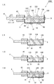
図1.Aは本発明の具体的な一実施例に係る光回路1000の構成を示す断面図である。光回路1000は、透明な光回路容器3の左端部に、接続部材43を用いて光ファイバ4のコア端面41がその内部に達するように接続されている。光回路容器3は45度の角度で傾斜して立設された波長選択性ミラー61及び62により3つの部屋に区分けされている。光ファイバ4のコア端面41が達している第1の部屋には、光ファイバ4のコア端面41から波長選択性ミラー61に達するコア110と、波長選択性ミラー61左面から光回路容器3底面に達する分岐51が形成されており、コア110と分岐51を包むようにクラッド210が固化充填されている。コア110と分岐51、クラッド210が光導波路を形成している。波長選択性ミラー61右面と波長選択性ミラー62左面に挟まれた第2の部屋には、波長選択性ミラー61左に形成されたコア110と光軸が一致している、コア120が波長選択性ミラー61右面から波長選択性ミラー62左面に達するよう形成されている。また、波長選択性ミラー62左面から光回路容器3底面に達する分岐52が形成されており、コア120と分岐52を包むようにクラッド220が固化充填されている。コア120と分岐52、クラッド220が光導波路を形成している。波長選択性ミラー62右面から光回路容器3右壁面までの第3の部屋には、波長選択性ミラー62左に形成されたコア120と光軸が一致している、コア130が波長選択性ミラー62右面から光回路容器3右壁面に達するよう形成されている。また、コア130を包むようにクラッド230が固化充填されている。コア130とクラッド230が光導波路を形成している。コア110、コア120、コア130は同一の光硬化性樹脂で形成されている。このうち、コア120には、波長λ2の光を吸収するが、波長λ1及び波長λ3の光を比較的吸収しない化合物が添加されている。
FIG. A is a cross-sectional view showing a configuration of an
光回路1000の、分岐51及び52並びにコア130に光結合するよう受光素子81及び82並びに発光素子9が設けられている。また、波長選択性ミラー61及び62の波長特性は、発光素子9の発光波長λ1に対しては、波長選択性ミラー61及び62のいずれも全透過するよう、受光素子81で受光すべき通信波長λ2に対しては波長選択性ミラー61において実質的に全反射するよう、受光素子82で受光すべき通信波長λ3に対しては波長選択性ミラー61において全透過し、波長選択性ミラー62において全反射するよう設定されている。これにより、左方向から光ファイバ4を介して導入される通信波長λ2の光は、コア110に導入された後、波長選択性ミラー61で反射されて分岐51に導入され、受光素子81で受光される。左方向から光ファイバ4を介して導入される通信波長λ3の光は、コア110に導入された後、波長選択性ミラー61で全透過されてコア120に導入され、波長選択性ミラー62で反射されて分岐52に導入され、受光素子82で受光される。逆に発光素子9からの発光波長λ1の光は、コア130に導入された後、波長選択性ミラー62で全透過されてコア120に導入され、波長選択性ミラー61で全透過されてコア110に導入され、端面41から光ファイバ4に導入される。
光ファイバ4のコア、光回路容器3の内部のコア110、コア120、コア130は全て光軸が一致しているので光ファイバ4のコアから光回路容器3の内部のコア110、コア120、コア130へと、あるいはその逆方向に光が伝送する際の伝送損失を理想的に低減させることが可能となっている。
Since the optical axis of the core of the
更に光回路1000においては、コア110に導入された後、波長選択性ミラー61において反射できず、一部コア120に通信波長λ2の光が漏れ出たとしても、コア120に添加されている波長λ2の光を吸収する化合物により当該光が吸収されるので、波長λ3の通信波長を受光すべき受光素子82としては、波長λ2の光に対しても感度を有するものを使用することが可能となる。こうして、感度範囲が広い、より安価な受光素子を受光素子82として使用することが可能となり、また、受光素子82に対するノイズを低減することが可能となる。このように、本発明を適用した光回路は、他の波長光の漏れ出しによるノイズを低減することを、容易に達成することが可能である。
Further, in the
本実施例の光回路1000の製造方法を次に説明する。図1.B乃至図1.Dは図1.Aの光回路1000の製造方法を示す工程図である。図1.Bのように、透明な光回路容器3の左端部に、接続部材43を用いて光ファイバ4のコア端面41が光回路容器3の内部に達するように接続する。また、光回路容器3の内部に波長選択性ミラー61及び62を設けて、光回路容器3の内部を3つの部屋に区分けする。波長選択性ミラー61及び62は光回路容器3の底面に垂直方向から45度左側に傾斜させて配設される。次に、未硬化の光硬化性樹脂(液)119、129、139を当該3つの部屋に充填する。これらは硬化させることで図1.Aのコア110、120、130となるものである。また、未硬化の光硬化性樹脂(液)129には、波長λ2の光を吸収するが、波長λ1及び波長λ3の光を比較的吸収しない化合物を添加しておく。次に光ファイバ4を介してコア端面41から樹脂硬化光を光回路容器3内部に照射する。当該樹脂硬化光は、波長選択性ミラー61及び62において、透過も反射もされ得る波長帯域を選択する。こうしてコアが自己形成的に硬化形成されるので、未硬化の光硬化性樹脂(液)を除去すれば、図1.Cのような分岐付きコアが形成される。この後、クラッド材料を各部屋に充填して固化させ、クラッド部210、220、230として各部屋の光導波路を完成させる。この後、受光素子81及び82並びに発光素子9を、各々分岐51、52、コア130と結合するよう付設して光回路1000を完成させる。
A method for manufacturing the
〔変形例〕
コア120に、特定波長に大きな吸収特性のある材料を用いず、クラッド220に大きな吸収特性のある材料を用いても効果があることが、次のように示された。この実験では図1.Aのコア130を形成しない、図2.Cのような構成とした。尚、波長選択性ミラー6と全反射ミラー7の構成とした。樹脂硬化波長(λw=488nm)から通信波長(λ1=530±20nm、および、λ2=660±20nm)において透明なアクリレート系光硬化性樹脂(ロックタイト社製、型式358、硬化後の屈折率1.52)をコア材料119、129として用いた。波長488nm、ファイバ端光出力250mWを照射すると各部屋に3次元のコア110、120及びそれらの分岐51及び52が形成される。各部屋に残留している未反応の光硬化性樹脂119及び129を除去し、続いて、クラッド210の材料として上記二つの通信波長帯において透明な低屈折率メタクリル系熱硬化性樹脂(三菱レイヨン社製、商品名「アクリボンド」、硬化後の屈折率1.49)を充填した。更に、クラッド220の材料として同じ低屈折率メタクリル系熱硬化性樹脂に顔料(東洋インキ製、型式6YS)を5.4wt%加えたものを充填し、室温で3時間硬化させた。得られた光導波路の伝送損失を、光スペクトラムアナライザにより計測した。図3の点線のグラフに示すように赤色(波長650nm近傍)に対して強い吸収を示し、緑色(波長530nm近傍)に対して透明である。このように、コアでなく、クラッドに吸収特性の大きい材料を用いても、上記実施例と同様の効果を期待することができる。尚、コア120に上記顔料を濃度0.027wt%添加した場合(クラッドへの顔料添加は無し)の伝送損失スペクトルも図3に実線で示した。
[Modification]
It has been shown as follows that the
光学フィルタ6として波長選択フィルタ(波長488nmにおいて透過率60%、波長530nmにおいて透過率93%、波長660nmにおいて反射率95%)を用いた場合、当該波長選択フィルタの不完全特性により第2の領域に漏光した波長660nm帯の光を該第2の部屋で選択的に吸収することにより、アイソレーションを約21dBに高めることが可能になった。第2の部屋に顔料を添加しない場合のアイソレーションは約10dBである。ここでは、クラッド220に減衰材料を適用した例を示したが、コア120に、もしくは、コア120及びクラッド220の両方に適用しても構わない。また、上記では顔料を用いた例を示したが、波長依存性のある光損失性材料として、この他、各種染料、着色(吸収波長スペクトルが一様でない)した有機材料、散乱性微粒子その他を用いることもできる。
When a wavelength selection filter (
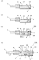
本実施例は、波長λ1の励起光により通信波長λ2の光の光増幅を行うための光回路に係るものである。図4.Cは本実施例に係る光回路2000の構成を示す断面図であり、図4.A及び図4.Bは、光回路2000の製造方法を示す工程図である。
The present embodiment relates to an optical circuit for performing optical amplification of light having a communication wavelength λ 2 by pumping light having a wavelength λ 1 . FIG. C is a cross-sectional view showing the configuration of the
光回路容器3に、その底面に対して斜め45度に傾斜した波長選択性ミラー6を設けて2つの部屋に区分けする。次に接続部材43を介して光ファイバ4を接続し、光ファイバ4のコアの端面41を光回路容器3の左側から波長選択性ミラー6の左側の部屋に達するように設ける。波長選択性ミラー6は波長λ1の励起光を全透過し、通信波長λ2を反射するものである。次に波長選択性ミラー6の左側の部屋に、希土類錯体、金属錯体若しくはレーザー色素等の、波長λ1の励起光により発光する発光材料が含まれた光硬化性樹脂をコア部材119として充填する。波長選択性ミラー6の右側の部屋には、当該発光材料が含まれない、波長λ1の励起光に対して透明な光硬化性樹脂をコア部材129として充填する。光ファイバ4の端面41からの紫外光等の照射により、図4.Bに示すように各部屋にコア110、分岐5、コア120が連続的に形成される。各部屋の未反応の光硬化性樹脂を除去し、クラッド210及びクラッド220の材料として励起波長λ1及び通信波長λ2において透明な光硬化性樹脂又は熱硬化性樹脂を充填して硬化させる。この後分岐5、コア120に結合させて受光素子8及び発光素子(励起光源)9を付設して光回路2000を完成させる。発光素子(励起光源)9の励起光(波長λ1)を、信号光(波長λ2)の進行方向である光ファイバ4からコア110、波長選択性ミラー6、分岐51とは逆方向である、コア120、波長選択性ミラー6、コア110の方向に入射させ、コア110内で発光材料に吸収させることにより励起させる。エネルギー状態の反転分布が生じるよう十分に励起された状態にある発光材料を含むコアを、信号光(波長λ2)が通過する際、誘導放出による増幅が可能となる。
The
実施例1の変形例のように、クラッド210に発光材料を添加しても良いが、その場合もコア110に発光材料を添加すると効果的であり、クラッドにおいても発光材料が励起されるように容器3の周囲から励起光λ1を照射するようにする。あるいは、上記受光素子8を発光素子に置き換えても良い。この場合は出力の小さい発光素子の発光出力を補強するものとなる。また、図4.Dの光回路2100のように構成しても良い。波長選択性ミラー60を波長選択性ミラー6と光回路容器3左端部との間に設け、波長選択性ミラー60と波長選択性ミラー6の間で光増幅を行い、波長選択性ミラー60と光回路容器3左端部との間はコア120、クラッド220とそれぞれ組成の同じコア100、クラッド200を設ける。波長選択性ミラー60は、波長λ1の励起光を全反射し、通信波長λ2の光を全透過するものとする。これにより波長λ1の励起光は、波長選択性ミラー60で反射されてコア110の発光部材に漏れなく吸収され、且つ光ファイバ4に漏れることが無い。よってより効果的で外部にノイズを出さない光回路(光増幅回路)とすることができる。
As in the modification of the first embodiment, a light emitting material may be added to the clad 210. However, in that case, it is effective to add a light emitting material to the
図5は4つの波長選択性ミラーを用いて、各ミラーを挟むコア同士が同一の組成でない5つのコア110、120、130、140、150を形成する、5分岐の光回路3000の形成方法を示す工程図である。図5.Aのように、光回路容器3に4つの波長選択性ミラー6を設けて5つの部屋に分割し、光ファイバ4を接続部材43により光回路容器3に接続して、光ファイバ4のコア端面を最も左の部屋に導入する。次にコア部材(光硬化性樹脂)119、129、139、149、159を5つの部屋にそれぞれ充填する。次に図5.Bのように、光ファイバ4を介して樹脂硬化光λWを導入し、コア110、120、130、140及び150並びに分岐51、52、53、54を自己形成的に硬化させて形成する。次に未硬化のコア部材(光硬化性樹脂)119、129、139、149、159を除去する(図5.C)。最後に各部屋にクラッド部材を充填し、紫外光又は加熱により硬化させてクラッド210、220、230、240、250を形成する(図5.D)。尚、各ミラーを挟むクラッド同士が同一の組成でない5つのクラッド210、220、230、240、250を形成しても良い。分岐51、52、53、54、コア150にそれぞれ受光素子又は発光素子を付設して、様々な機能を各コア又は分岐に持たせた、一体型の光回路とすることが可能である。
FIG. 5 shows a method of forming a five-branch
図6.Aは、非線形媒質を用いた光回路4000の構成を示す断面図である。図6.Aの光回路4000は、非線形媒質をコア120に用い、当該コアの形成された部屋を通信波長光に対して透明な電極63及び64で挟んだ構成である。電極63の左側のコア110、クラッド210、電極64の右側のコア130、クラッド230は単なる光導波路を形成するに過ぎない。このような光回路4000は、電極63と64の間に電場を印加することで、光ファイバ4から受光素子9に向かう光の強度をコア120において変化させることができる。このような性質を有するコア120の材料としては、ポリエチレンオキシドや液晶分子を含有させたポリマを使用する。コア120は電極63及び64による電場の印加により、クラッド220との比屈折率差が変化することで上記性質を有するものである。尚、電極63及び64に重ねて、偏光フィルタを設け、発光素子9として偏光発光素子を用いあるいは所望の偏光のみ検出できる受光素子に置き換えても良い。
FIG. A is a cross-sectional view showing a configuration of an
図6.Bは、光シャッターを用いた光回路5000の構成を示す断面図である。図6.Bの光回路5000は、光シャッター65を設けたものである。光シャッター65の左側のコア110、クラッド210、及び右側のコア120、クラッド220は単なる光導波路を形成するに過ぎない。光シャッター65に電位を印加することで、光ファイバ4から受光素子9に向かう光の透過及び遮断を切り替えることができる。光シャッター65としては、非線形光学結晶、圧電材料、液晶板を用いることができる。
FIG. B is a cross-sectional view showing a configuration of an
〔応用例〕
これら図6.Aの光回路4000及び図6.Bの光回路5000の要部を、上記実施例1、2の要部と組み合わせることで、即ち実施例3のような多区画の光回路に実施例1、2、4の要部を実現することで、従来複数個の光回路を連結して構成する必要があった光モジュールを、1個の光回路容器に集積することが可能となる。且つ、光硬化性樹脂(液)を用いた自己形成によるコア形成により、各コアの光軸は自動的に一致するものであり、且つ小型化が極めて容易となる。
[Application example]
These FIG. A
上記各実施例においては、コアを自己形成的に形成した後、未硬化樹脂(液)を除去して、別途クラッド材を充填し、固化させる方法を採用しているが、次のような製造方法により「自己形成的に」コアを形成した後、周りの未硬化の光硬化性樹脂(液)を硬化させて、クラッドを形成しても良い。 In each of the above embodiments, a method is employed in which after the core is formed in a self-forming manner, the uncured resin (liquid) is removed, and a cladding material is separately filled and solidified. After forming the core “self-formingly” by the method, the surrounding uncured photocurable resin (liquid) may be cured to form a clad.
各部屋のコア及びクラッドは各々1種類の混合樹脂溶液を用いる。混合樹脂溶液は、コア形成波長(樹脂硬化光の波長)λwにおいて硬化可能な高屈折率の第1の光硬化性樹脂液(モノマ及び/又はオリゴマ」と、λwにおいて硬化しない低屈折率の第2の光硬化性樹脂液(モノマ及び/又はオリゴマ)とを混合して作製する。これら第1及び第2の光硬化性樹脂液は共重合しない材料を選ぶことが必要である。例えば、ラジカル重合とカチオン重合の組み合わせが有効である。ラジカル重合の樹脂材料としては、(メタ)アクリル系があり、カチオン重合の樹脂材料としてはエポキシ系、オキセタン系がある。必要な部屋には、これらの混合液中に特定波長帯においての損失性材料を分散、溶解若しくは分子結合により含有させる。 A single mixed resin solution is used for the core and the clad of each room. The mixed resin solution is composed of a high refractive index first photocurable resin liquid (monomer and / or oligomer) that can be cured at the core forming wavelength (wavelength of resin curing light) λw, and a low refractive index first resin that is not cured at λw. It is necessary to select a material that does not copolymerize the first and second photocurable resin liquids, for example, radicals. A combination of polymerization and cationic polymerization is effective. (Meth) acrylic resins are used as radical polymerization resin materials, and epoxy and oxetane resins are used as cationic polymerization resin materials. A lossy material in a specific wavelength band is contained in the mixed solution by dispersing, dissolving, or molecular bonding.
このような混合樹脂溶液に、光ファイバを介して若しくは直接、レーザビーム(樹脂硬化光)を照射することにより、高屈折率材料が選択的に硬化し、重合による屈折率増加により、この重合物内に光がトラップされ、光軸方向に連続的に重合が進むことで混合溶液中に高屈折率材料成分が多い硬化物(コア)を形成することができる。この際、未硬化の低屈折率材料成分が高屈折率材料成分が多い硬化物(コア)外部へ拡散可能なよう、樹脂硬化光の強度を調整し、あるいは低屈折率の第2の光硬化性樹脂液(モノマ及び/又はオリゴマ)として低分子量のもの、即ち粘度の低いものを用いる。コアが形成された後、各部屋の未硬化の混合樹脂溶液全体を紫外線で一括硬化させる。コアは高屈折率成分がクラッドより多いので、クラッドの硬化後も導波構造が維持される。 By irradiating such a mixed resin solution with an optical fiber or directly with a laser beam (resin curing light), the high refractive index material is selectively cured, and this polymer is increased due to an increase in the refractive index due to polymerization. Light is trapped inside, and polymerization proceeds continuously in the optical axis direction, whereby a cured product (core) having a high refractive index material component in the mixed solution can be formed. At this time, the intensity of the resin curing light is adjusted so that the uncured low refractive index material component can be diffused outside the cured product (core) having a high high refractive index material component, or the second photocuring with a low refractive index is performed. As the conductive resin liquid (monomer and / or oligomer), one having a low molecular weight, that is, one having a low viscosity is used. After the core is formed, the entire uncured mixed resin solution in each room is collectively cured with ultraviolet rays. Since the core has a higher refractive index component than the cladding, the waveguide structure is maintained even after the cladding is cured.
ラジカル重合の樹脂材料として、アクリル系光硬化性樹脂(ロックタイト社製品番358、硬化後の屈折率1.52)、カチオン重合の樹脂材料としてエポキシ系光硬化性樹脂(ダイキン社製、品番UV−1100、硬化後の屈折率1.43)をそれぞれ質量比8:2で混合させた。これを透明樹脂容器に充填して、波長488nm、強度200mWのArレーザ光をコア径100μmの石英ファイバを介して、この混合樹脂に照射することにより自己形成形の光導波路のコアを形成した。 As a resin material for radical polymerization, an acrylic photocurable resin (Loctite product number 358, refractive index 1.52 after curing), and as a cationic polymerization resin material, an epoxy photocurable resin (manufactured by Daikin, product number UV-1100, Refractive index 1.43) after curing was mixed at a mass ratio of 8: 2, respectively. This was filled in a transparent resin container, and this mixed resin was irradiated with Ar laser light having a wavelength of 488 nm and an intensity of 200 mW through a quartz fiber having a core diameter of 100 μm to form a self-forming optical waveguide core.
この際光増幅器となる部分については光硬化性樹脂液に、テルビウム(III)トリスアセチルアセトナートを1質量%以上分散させた後にコアを形成した。この後全体をUV硬化させることにより、波長545nm帯の光増幅機能を発現させることができた。 At this time, for the portion to be an optical amplifier, a core was formed after dispersing 1% by mass or more of terbium (III) trisacetylacetonate in a photocurable resin liquid. Thereafter, the whole was UV-cured, and an optical amplification function in a wavelength of 545 nm band could be expressed.
本実施例は最初に形成する「コアの外周部」に低屈折率成分が集中する製造方法によるものである。本実施例による光導波路は、コア中心から、高屈折率部分、狭い(薄皮状の)低屈折率部分、高屈折率部分と、屈折率分布が連続的ではあるが低屈折率部分が急峻な谷状を示す導波路となる。混合樹脂溶液として、コア形成波長(樹脂硬化光の波長)λwにおいて硬化可能な低屈折率の第1の光硬化性樹脂液(モノマ及び/又はオリゴマ)と、λwにおいて硬化しない高屈折率の第2の光硬化性樹脂液(モノマ及び/又はオリゴマ)とを混合して作製する。本実施例においても、これら第1及び第2の光硬化性樹脂液は共重合しない材料を選ぶことが必要である。例えば、ラジカル重合とカチオン重合の組み合わせが有効である。ラジカル重合の樹脂材料としては、(メタ)アクリル系があり、カチオン重合の樹脂材料としてはエポキシ系、オキセタン系がある。必要な部屋には、これらの混合液中に特定波長帯においての損失性材料を分散、溶解若しくは分子結合により含有させる。 This embodiment is based on the manufacturing method in which the low refractive index component concentrates on the “outer peripheral portion of the core” formed first. The optical waveguide according to this example has a high refractive index portion, a narrow (thin skin) low refractive index portion, and a high refractive index portion from the center of the core, and the refractive index distribution is continuous but the low refractive index portion is steep. It becomes a waveguide showing a valley shape. As a mixed resin solution, a low refractive index first photocurable resin liquid (monomer and / or oligomer) that can be cured at a core formation wavelength (wavelength of resin curing light) λw, and a high refractive index first that does not cure at λw. Two photo-curing resin liquids (monomer and / or oligomer) are mixed to produce. Also in this example, it is necessary to select a material that does not copolymerize the first and second photocurable resin liquids. For example, a combination of radical polymerization and cationic polymerization is effective. The resin material for radical polymerization includes (meth) acrylic resin, and the resin material for cationic polymerization includes epoxy resin and oxetane resin. In a necessary room, a lossy material in a specific wavelength band is contained in these mixed liquids by dispersion, dissolution, or molecular bonding.
ラジカル重合の樹脂材料として、アクリル系光硬化性樹脂(ロックタイト社製品番358、硬化後の屈折率1.52)、カチオン重合の樹脂材料としてエポキシ系光硬化性樹脂(ダイキン社製、品番UV−4000、硬化後の屈折率1.541)をそれぞれ質量比7:3で混合させた。これを透明樹脂容器に充填して、波長488nm、強度350mWのArレーザ光をコア径100μmの石英ファイバを介して、この混合樹脂に照射することにより自己形成形の光導波路のコアを形成した。 As a radical polymerization resin material, an acrylic photocurable resin (Loctite product number 358, refractive index 1.52 after curing), and as a cationic polymerization resin material, an epoxy photocurable resin (manufactured by Daikin, product number UV-4000, Refractive index 1.541) after curing was mixed at a mass ratio of 7: 3, respectively. This was filled in a transparent resin container and irradiated with Ar laser light having a wavelength of 488 nm and an intensity of 350 mW through a quartz fiber having a core diameter of 100 μm to form a core of a self-forming optical waveguide.
この際光増幅器となる部分については光硬化性樹脂液に、テルビウム(III)トリスアセチルアセトナートを1質量%以上分散させた後にコアを形成した。この後全体をUV硬化させることにより、波長545nm帯の光増幅機能を発現させることができた。 At this time, for the portion to be an optical amplifier, a core was formed after dispersing 1% by mass or more of terbium (III) trisacetylacetonate in a photocurable resin liquid. Thereafter, the whole was UV-cured, and an optical amplification function in a wavelength of 545 nm band could be expressed.
本実施例においては、高屈折率の第2の光硬化性樹脂液の拡散速度に比して、コア部分の低屈折率の光硬化性樹脂硬化物の成長速度が十分大きくなるような光強度により光ファイバを介して、若しくは直接レーザービームを照射する。「コア部分」は、高屈折率の第2の光硬化性樹脂液を含有しながら低屈折率材料が選択的に硬化し、重合による屈折率増加により、この重合物内に光がトラップされ、光軸方向に連続的に重合が進むことで、混合溶液中の高屈折率材料と低屈折率材料の成分比とほぼ同じ成分比で硬化物(コア)を形成することができる。その後、コア内からの放射光、散乱光、染みだし光により「コア部分」である硬化物外周部に低屈折率樹脂がゆっくり選択的に硬化成長する。この際、低屈折率樹脂硬化物中にトラップされた液状部分については、低屈折率モノマ(オリゴマ)の濃度が極めて小さい。そこで外部の未硬化の光硬化性樹脂溶液から低屈折率モノマ(オリゴマ)が硬化物(コア)内部の液状部分に拡散することになる。しかし硬化物(コア)中心部へは拡散が遅い。結局,硬化物(コア)外周部の「薄皮状」の領域のみ、低屈折率樹脂硬化物中にトラップされた液状部分について、未硬化の高屈折率成分及び未硬化の低屈折率成分の比が、外部の未硬化の光硬化性樹脂溶液のそれと同じ又は近いものとなる。この部分は、硬化済みの低屈折率樹脂を勘案すると、低屈折率成分が多い状態である。そこで最後に、未硬化の樹脂液を全て、即ち硬化物にトラップされたままのものも、硬化物の外部のものも、紫外線で硬化させる。実質的なクラッドとなる低屈折率層はコア外周部に薄皮状に形成される。その外部は子を中心部と同じか略等しい屈折率を有するものとなる。 In this example, the light intensity is such that the growth rate of the low refractive index photocurable resin cured product of the core portion is sufficiently higher than the diffusion rate of the second refractive resin liquid having a high refractive index. The laser beam is irradiated through an optical fiber or directly. The “core portion” contains a second photocurable resin liquid having a high refractive index, and a low refractive index material is selectively cured, and light is trapped in the polymer due to an increase in the refractive index due to polymerization. By continuously proceeding the polymerization in the optical axis direction, a cured product (core) can be formed with a component ratio substantially the same as the component ratio of the high refractive index material and the low refractive index material in the mixed solution. Thereafter, the low refractive index resin slowly and selectively grows on the outer peripheral portion of the cured product, which is the “core portion”, by radiated light, scattered light, and oozing light from the core. At this time, the concentration of the low refractive index monomer (oligomer) is extremely small in the liquid portion trapped in the low refractive index resin cured product. Therefore, the low refractive index monomer (oligomer) diffuses from the external uncured photocurable resin solution into the liquid portion inside the cured product (core). However, the diffusion to the center of the cured product (core) is slow. As a result, the ratio of the uncured high refractive index component and the uncured low refractive index component for the liquid part trapped in the low refractive index resin cured product only in the “thin skin” region on the outer periphery of the cured product (core). Is the same as or close to that of the external uncured photocurable resin solution. This portion is in a state where there are a lot of low refractive index components in consideration of the cured low refractive index resin. Therefore, finally, all of the uncured resin liquid, that is, the one that is trapped in the cured product and the one that is outside the cured product are cured with ultraviolet rays. The low-refractive index layer that becomes a substantial cladding is formed in a thin skin shape on the outer periphery of the core. The outside has a refractive index that is the same as or substantially equal to the center of the child.
図7.Aは、実施例1乃至5の導波路の屈折率分布であり、図7.Bは、実施例6の導波路の屈折率分布であり、図7.Cは、実施例7の導波路の屈折率分布である。各々導波路の断面に沿った屈折率分布を示した。図7.Aのように、実施例1乃至5における屈折率分布は、コア部分が一定の屈折率を、その外部のクラッド部分が一定の屈折率を有する。コアとクラッドの境界部分において、ステップ状に屈折率が変化する。一方、図7.Bのように、実施例6における屈折率分布は、コアとクラッドの境界部分において、なだらかに連続的変化する。また、図7.Cのように、実施例7における屈折率分布は、コア外周部に薄皮状にクラッドが形成され、その外部は、コア中心部とほぼ同じ屈折率を有することとなる。 FIG. A is the refractive index distribution of the waveguides of Examples 1 to 5, and FIG. B is the refractive index profile of the waveguide of Example 6, and FIG. C is the refractive index profile of the waveguide of Example 7. Refractive index distribution along the cross section of each waveguide is shown. FIG. Like A, the refractive index distribution in Examples 1 to 5 has a constant refractive index in the core portion and a constant refractive index in the outer cladding portion. The refractive index changes stepwise at the boundary between the core and the clad. On the other hand, FIG. Like B, the refractive index distribution in Example 6 changes gently and continuously at the boundary between the core and the cladding. FIG. As in C, in the refractive index distribution in Example 7, a thin clad is formed on the outer peripheral portion of the core, and the outside thereof has substantially the same refractive index as that of the core central portion.
1000、2000、2100、3000、4000、5000:光回路
100、110、120、130、140、150:コア
119、129、139、149、159:コア部材
200、210、220、230、240、250:クラッド
3:光回路容器
4:光ファイバ
41:光ファイバのコア
43:接続部材
5、51、52、53、54:コアの分岐
6、60、61、62:波長選択性ミラー
63、64:透明電極
65:光シャッター
7:全反射ミラー
8、81、82:受光素子
9:発光素子
1000, 2000, 2100, 3000, 4000, 5000:
Claims (14)
光導波路のコア形成のための樹脂硬化光を導入する窓を有する光回路容器に1個以上のフィルタ素子を配置させ、且つ前記各フィルタ素子を含む隔壁にて前記光回路容器を2個以上の部屋に区分けし、
前記2個以上の部屋のうち前記樹脂硬化光を導入する窓を有する部屋を含む2個以上の部屋の各々に、未硬化の光硬化性樹脂を充填し、
前記窓から前記樹脂硬化光を導入することにより、各部屋の光硬化性樹脂を硬化させて、各前記フィルタ素子を挟む各前記コアの光軸が一致するように当該各コアを形成し、
各部屋における前記各コアの周囲に、クラッドを形成し、
前記フィルタ素子の少なくとも1個について、当該フィルタ素子を挟んで両側の部屋に充填される光硬化性樹脂の成分又はその光硬化性樹脂に対する添加物を異ならせることにより、当該フィルタ素子を挟んで両側に形成される2つのコアの組成又は添加物が異なるようにし、及び/又は、当該2つのコアをそれぞれ取り巻く2つのクラッドを構成する材料の組成又はその材料に対する添加物を異ならせることにより、その2つのクラッドの組成又は添加物が異なるようにした
ことを特徴とする光回路の製造方法。 In a method of manufacturing an optical circuit having an axial core made of a cured product of a photocurable resin,
One or more filter elements are arranged in an optical circuit container having a window for introducing resin-cured light for forming a core of an optical waveguide, and two or more optical circuit containers are separated by a partition including the filter elements. Divided into rooms,
Filling each of two or more rooms including a room having a window for introducing the resin-curing light among the two or more rooms with an uncured photocurable resin,
By introducing the resin curing light from the window, the photocurable resin in each room is cured, and each core is formed so that the optical axes of the cores sandwiching each filter element coincide with each other ,
Form a cladding around each core in each room,
For at least one of the filter elements, both sides of the filter element are sandwiched by differentiating the components of the photocurable resin filled in the chambers on both sides of the filter element or additives to the photocurable resin. By making the composition or additive of the two cores formed different from each other and / or by making the composition of the two clads constituting the two cores surrounding each of the two cores different or the additive to the material. A method of manufacturing an optical circuit, wherein the composition or additive of two clads are different .
当該波長選択性ミラーを分岐点とする分岐コアが形成されることを特徴とする請求項1に記載の光回路の製造方法。 At least one of the filter elements is a wavelength selective mirror,
The method of manufacturing an optical circuit according to claim 1, characterized in that the branch core to the branch point the wavelength-selective mirror is formed.
一方には、励起光により伝送光の強度を増幅させるための添加物が添加され、
他方には前記添加物が添加されないことを特徴とする請求項2に記載の光回路の製造方法。 Of the two cores sandwiching the wavelength selective mirror,
On the other hand, an additive for amplifying the intensity of the transmitted light by the excitation light is added ,
The method of manufacturing an optical circuit according to claim 2 on the other, characterized in Lena Ikoto is added the additive.
前記コアを形成した後、未硬化の光硬化性樹脂を前記光回路容器から除去し、
クラッド材料を充填することを特徴とする請求項1乃至請求項6のいずれか1項に記載の光回路の製造方法。 For at least one of the rooms
After forming the core, uncured photocurable resin is removed from the optical circuit container,
The method for manufacturing an optical circuit according to claim 1 , wherein a clad material is filled.
前記未硬化の光硬化性樹脂は、より長波長の光で硬化する高屈折率の第1の光硬化性樹脂液と、より短波長の光で硬化する、又は熱硬化する低屈折率の第2の光硬化性樹脂液との混合物であって、
前記第1の光硬化性樹脂液を硬化させるが前記第2の光硬化性樹脂液を硬化させない波長の前記樹脂硬化光を導入することで、高屈折率の第1の光硬化性樹脂液の硬化物の含有率の高いコアを形成した後、
残余の未硬化の光硬化性樹脂を硬化させることで低屈折率のクラッド部分を形成することを特徴とする請求項1乃至請求項6のいずれか1項に記載の光回路の製造方法。 For at least one of the rooms
The uncured photocurable resin includes a first photocurable resin liquid having a high refractive index that is cured by light having a longer wavelength, and a first resin having a low refractive index that is cured by light having a shorter wavelength or is thermally cured. A mixture of the photocurable resin liquid of No. 2,
By introducing the resin curing light having a wavelength that cures the first photocurable resin liquid but does not cure the second photocurable resin liquid, the first photocurable resin liquid having a high refractive index is introduced. After forming a core with a high content of cured product,
7. The method of manufacturing an optical circuit according to claim 1, wherein the remaining uncured photo-curable resin is cured to form a low refractive index clad portion.
前記未硬化の光硬化性樹脂は、より長波長の光で硬化する低屈折率の第1の光硬化性樹脂液と、より短波長の光で硬化する、又は熱硬化する高屈折率の第2の光硬化性樹脂液の混合物であって、
前記第1の光硬化性樹脂液を硬化させるが前記第2の光硬化性樹脂液を硬化させない波長の前記樹脂硬化光を導入することで、低屈折率の第1の光硬化性樹脂液の硬化物に未硬化の前記第1及び第2の光硬化性樹脂液が取り込まれた状態を形成した後、残余の未硬化の光硬化性樹脂を硬化させることで、高屈折率のコアと、その外周部の第1の光硬化性樹脂液の硬化物の含有率が高い低屈折率のクラッド部分と、その残余の外側の高屈折率部分を形成することを特徴とする請求項1乃至請求項6のいずれか1項に記載の光回路の製造方法。 For at least one of the rooms
The uncured photocurable resin includes a low refractive index first photocurable resin liquid that cures with longer wavelength light, and a high refractive index first that cures or heat cures with shorter wavelength light. A mixture of two photocurable resin liquids,
By introducing the resin curing light having a wavelength that cures the first photocurable resin liquid but does not cure the second photocurable resin liquid, the first photocurable resin liquid having a low refractive index is introduced. After forming a state in which the uncured first and second photocurable resin liquids are taken into the cured product, by curing the remaining uncured photocurable resin, a high refractive index core, a first cladding portion of the high content of low refractive index of the cured product of the photocurable resin liquid of the outer peripheral portion, claims 1 to, characterized in that to form a high refractive index portion of the outside of the remaining Item 7. The method for manufacturing an optical circuit according to any one of Items 6 to 6 .
前記未硬化の光硬化性樹脂は、より長波長の光で硬化する高屈折率の光硬化性樹脂液と、低屈折率の熱硬化性樹脂液との混合物であって、
前記光硬化性樹脂液を硬化させるが前記熱硬化性樹脂液を硬化させない波長の前記樹脂硬化光を導入することで、高屈折率の光硬化性樹脂液の硬化物の含有率の高いコアを形成した後、
残余の未硬化の光硬化性樹脂及び熱硬化性樹脂を硬化させることで低屈折率のクラッド部分を形成することを特徴とする請求項1乃至請求項6のいずれか1項に記載の光回路の製造方法。 For at least one of the rooms
The uncured photocurable resin is a mixture of a high refractive index photocurable resin liquid that is cured with light having a longer wavelength and a low refractive index thermosetting resin liquid,
By introducing the resin curing light having a wavelength that cures the photocurable resin liquid but does not cure the thermosetting resin liquid, a core with a high content of a cured product of a high refractive index photocurable resin liquid is obtained. After forming
The optical circuit according to any one of claims 1 to 6, wherein a clad portion having a low refractive index is formed by curing the remaining uncured photocurable resin and thermosetting resin. Manufacturing method.
前記未硬化の光硬化性樹脂は、より長波長の光で硬化する低屈折率の光硬化性樹脂液と、高屈折率の熱硬化性樹脂液との混合物であって、
前記光硬化性樹脂液を硬化させるが前記熱硬化性樹脂液を硬化させない波長の前記樹脂硬化光を導入することで、低屈折率の光硬化性樹脂液の硬化物に未硬化の前記光硬化性樹脂液及び熱硬化性樹脂液が取り込まれた状態を形成した後、残余の未硬化の光硬化性樹脂及び熱硬化性樹脂液を硬化させることで、高屈折率のコアと、その外周部の光硬化性樹脂液の硬化物の含有率が高い低屈折率のクラッド部分と、その残余の外側の高屈折率部分を形成することを特徴とする請求項1乃至請求項6のいずれか1項に記載の光回路の製造方法。 For at least one of the rooms
The uncured photocurable resin is a mixture of a low refractive index photocurable resin liquid that is cured with light of a longer wavelength and a high refractive index thermosetting resin liquid,
By introducing the resin curing light having a wavelength that cures the photocurable resin liquid but does not cure the thermosetting resin liquid, the uncured photocured resin is cured into a cured product of a low refractive index photocurable resin liquid. After forming the state in which the curable resin liquid and the thermosetting resin liquid are taken in, the remaining uncured photocurable resin and the thermosetting resin liquid are cured, and the high refractive index core and the outer peripheral portion thereof. and a cladding portion of the high content of low refractive index of the cured product of the photocurable resin liquid, any one of claims 1 to 6, characterized in that to form a high refractive index portion of the outside of the remaining the method of manufacturing an optical circuit according to claim.
当該光ファイバ端面が、前記窓を有する部屋に充填された未硬化の光硬化性樹脂中に浸漬された状態で前記樹脂硬化光を前記光ファイバを介して導入することを特徴とする請求項1乃至請求項13のいずれか1項に記載の光回路の製造方法。 From the window through which the resin curing light is introduced, an optical fiber is introduced into the room,
Claim the optical fiber end face, and wherein said resin curing light while being immersed in the photo-curable resin of the uncured filled the room with the window be introduced through the optical fiber 1 The method for manufacturing an optical circuit according to claim 13 .
Priority Applications (1)
| Application Number | Priority Date | Filing Date | Title |
|---|---|---|---|
| JP2004065385A JP4352944B2 (en) | 2004-03-09 | 2004-03-09 | Optical circuit manufacturing method |
Applications Claiming Priority (1)
| Application Number | Priority Date | Filing Date | Title |
|---|---|---|---|
| JP2004065385A JP4352944B2 (en) | 2004-03-09 | 2004-03-09 | Optical circuit manufacturing method |
Publications (2)
| Publication Number | Publication Date |
|---|---|
| JP2005257741A JP2005257741A (en) | 2005-09-22 |
| JP4352944B2 true JP4352944B2 (en) | 2009-10-28 |
Family
ID=35083561
Family Applications (1)
| Application Number | Title | Priority Date | Filing Date |
|---|---|---|---|
| JP2004065385A Expired - Fee Related JP4352944B2 (en) | 2004-03-09 | 2004-03-09 | Optical circuit manufacturing method |
Country Status (1)
| Country | Link |
|---|---|
| JP (1) | JP4352944B2 (en) |
Families Citing this family (7)
| Publication number | Priority date | Publication date | Assignee | Title |
|---|---|---|---|---|
| JP4592628B2 (en) * | 2006-03-28 | 2010-12-01 | 株式会社豊田中央研究所 | Manufacturing method of optical module |
| JP4544210B2 (en) * | 2006-06-21 | 2010-09-15 | 豊田合成株式会社 | Optical module and manufacturing method thereof |
| JP2008277547A (en) * | 2007-04-27 | 2008-11-13 | Kyoto Institute Of Technology | Method for manufacturing optical amplifier |
| JP2009015214A (en) * | 2007-07-09 | 2009-01-22 | Tokai Univ | Method of manufacturing self-forming optical waveguide |
| JP2010054623A (en) | 2008-08-26 | 2010-03-11 | Ricoh Co Ltd | Two-photon absorption material and its use |
| WO2013002013A1 (en) * | 2011-06-27 | 2013-01-03 | 学校法人 慶應義塾 | Optical waveguide and method for manufacturing same |
| JP2013174831A (en) * | 2012-02-27 | 2013-09-05 | Sumitomo Bakelite Co Ltd | Optical waveguide connection structure and electronic apparatus |
-
2004
- 2004-03-09 JP JP2004065385A patent/JP4352944B2/en not_active Expired - Fee Related
Also Published As
| Publication number | Publication date |
|---|---|
| JP2005257741A (en) | 2005-09-22 |
Similar Documents
| Publication | Publication Date | Title |
|---|---|---|
| Xiao et al. | On-chip mode converter based on two cascaded Bragg gratings | |
| US7450811B2 (en) | Optical waveguide device and optical modulator | |
| US8160414B1 (en) | Self forming waveguides for optical coupling and methodologies for making same | |
| CN101840126A (en) | Silicon-based cascaded resonant cavity all-optical logical AND gate structure capable of reducing power consumption | |
| JP3444352B2 (en) | Optical transmission line manufacturing method | |
| JP4352944B2 (en) | Optical circuit manufacturing method | |
| Lenin Babu et al. | 4-Channel DWDM demultiplexer on silicon photonic crystal slab | |
| JP6871137B2 (en) | Hybrid optical circuit | |
| US7024072B2 (en) | Fiber-optic tunable filter and intensity modulater | |
| JP2002258095A (en) | Method of forming optical waveguide | |
| JP4024031B2 (en) | Manufacturing method of optical waveguide | |
| Mondal et al. | All-Optical Demultiplexer: A Review on Recent Research and Developments | |
| WO2023079720A1 (en) | Optical element, optical integrated element, and method for manufacturing optical integrated element | |
| JP3750671B2 (en) | Manufacturing method of optical transmission line | |
| WO2024121894A1 (en) | Optical element and method for manufacturing optical element | |
| WO2020158588A1 (en) | Optical circuit | |
| Nabiei et al. | Design of high isolation ratio optical isolators based on magneto-optical plasmonic waveguides | |
| JP2000147291A (en) | Method and device for manufacturing optical waveguide element | |
| JP2018036433A (en) | Hybrid optical circuit | |
| JP4211526B2 (en) | Optical transmission path and photocurable resin solution for optical transmission path formation | |
| JPH05249447A (en) | Optical fiber modulator | |
| Bekele et al. | Fano Resonances for Realizing Compact and Low Energy Consumption Photonic Switches | |
| Geuzebroek et al. | From Chip to Module: Silicon-Nitride for Visible Light | |
| US20070025660A1 (en) | All-optical variable optical attenuator | |
| Rabiei et al. | Polymer microring resonators |
Legal Events
| Date | Code | Title | Description |
|---|---|---|---|
| A621 | Written request for application examination |
Free format text: JAPANESE INTERMEDIATE CODE: A621 Effective date: 20070305 |
|
| A977 | Report on retrieval |
Free format text: JAPANESE INTERMEDIATE CODE: A971007 Effective date: 20081217 |
|
| A131 | Notification of reasons for refusal |
Free format text: JAPANESE INTERMEDIATE CODE: A131 Effective date: 20090303 |
|
| A521 | Written amendment |
Free format text: JAPANESE INTERMEDIATE CODE: A523 Effective date: 20090427 |
|
| A711 | Notification of change in applicant |
Free format text: JAPANESE INTERMEDIATE CODE: A711 Effective date: 20090527 |
|
| A521 | Written amendment |
Free format text: JAPANESE INTERMEDIATE CODE: A821 Effective date: 20090527 |
|
| TRDD | Decision of grant or rejection written | ||
| A01 | Written decision to grant a patent or to grant a registration (utility model) |
Free format text: JAPANESE INTERMEDIATE CODE: A01 Effective date: 20090707 |
|
| A01 | Written decision to grant a patent or to grant a registration (utility model) |
Free format text: JAPANESE INTERMEDIATE CODE: A01 |
|
| A61 | First payment of annual fees (during grant procedure) |
Free format text: JAPANESE INTERMEDIATE CODE: A61 Effective date: 20090720 |
|
| FPAY | Renewal fee payment (event date is renewal date of database) |
Free format text: PAYMENT UNTIL: 20120807 Year of fee payment: 3 |
|
| FPAY | Renewal fee payment (event date is renewal date of database) |
Free format text: PAYMENT UNTIL: 20120807 Year of fee payment: 3 |
|
| S531 | Written request for registration of change of domicile |
Free format text: JAPANESE INTERMEDIATE CODE: R313532 |
|
| FPAY | Renewal fee payment (event date is renewal date of database) |
Free format text: PAYMENT UNTIL: 20120807 Year of fee payment: 3 |
|
| R350 | Written notification of registration of transfer |
Free format text: JAPANESE INTERMEDIATE CODE: R350 |
|
| FPAY | Renewal fee payment (event date is renewal date of database) |
Free format text: PAYMENT UNTIL: 20120807 Year of fee payment: 3 |
|
| FPAY | Renewal fee payment (event date is renewal date of database) |
Free format text: PAYMENT UNTIL: 20130807 Year of fee payment: 4 |
|
| LAPS | Cancellation because of no payment of annual fees |