JP4347918B2 - Highly integrated TV tuner on a single microcircuit - Google Patents
Highly integrated TV tuner on a single microcircuit Download PDFInfo
- Publication number
- JP4347918B2 JP4347918B2 JP14842197A JP14842197A JP4347918B2 JP 4347918 B2 JP4347918 B2 JP 4347918B2 JP 14842197 A JP14842197 A JP 14842197A JP 14842197 A JP14842197 A JP 14842197A JP 4347918 B2 JP4347918 B2 JP 4347918B2
- Authority
- JP
- Japan
- Prior art keywords
- signal
- mixer
- mhz
- video
- tuner
- Prior art date
- Legal status (The legal status is an assumption and is not a legal conclusion. Google has not performed a legal analysis and makes no representation as to the accuracy of the status listed.)
- Expired - Lifetime
Links
Images


Description
【0001】
【発明の属する技術分野】
本発明はテレビチューナー回路に関し、特に、単一マイクロ回路デバイス内に組み立てられた高集積テレビチューナーに関する。
【0002】
【従来の技術】
テレビ製造における最も重要なコストの一つは、チューナーのコストである。テレビ(TV)チューナーの典型的コストは、約$15,000であり、かつそれは、テレビ受信機全体のコストに対して、相当大きい。チューナーコストを減少させる解決策の一つは、チューナーの部品数を減らすことである。
【0003】
伝統的に、チューナーは2つの基本的要素から構成される。第一の要素は、高周波数の中間周波数への変換(RF to IF)をする。その後、第二の要素が、IFをベースバンドに変換する。TVチューナーは、本来ブラウン管を包含するスタンドアロンユニットであるテレビ受信機内でテレビ放送を受信するために元来設計された。そのため、TVチューナーは元来単一目的のデバイスに埋め込まれた集積部品であった。
【0004】
しかしながら、現在、最先端消費者電子デバイスは、テレビ受信機の組み込み部品ではないTVチューナーを使用する。このチューナーは、ある点でブラウン管に接続されている分離要素であるが、しかしこのチューナーは、モニターの一体の部品ではない。例えば、TVチューナーは、回路ボード上に組み立て、それからパーソナルコンピュータ(PC)システムに取り付け、それによって、このPCをテレビ受信機として機能させることができる。これらのチューナーは、無線周波テレビ信号をベースバンド(又は低周波数)ビデオ信号に変換し、かつこれは、それからビデオ処理用途のためにPC内の他の要素に伝送することができる。
【0005】
RF-to-IF変換を実行する回路要素は典型的には、1つ乃至は2つの集積回路と多数の個別要素--インダクタ、キャパシタ、及び/又はトランジスタから構成される。IF-to-ベースバンド変換は典型的には、別の集積回路、セラミックフィルタ及びSAWフィルタのようないくつかのフィルタ要素、抵抗器及びポテンショメータのような一連のチューニング及び制御要素、可変インダクタ及び/又はキャパシタ、及びいくつかの追加の外部要素を包含している。このように、チューナーの複雑さはかなり高く、そして典型的には、回路ボード上に100から200の要素がある。さらに、最先端TVチューナーは、各チューナーが工場を離れる前にマニュアルチューニングによって調整することを依然として必要としている。このマニュアルチューニングは、製造プロセスと関連した最も高価なコストのかかるものの一つであり、チューナーのコストにおける重要なファクタとなっている。
【0006】
過去の放送テレビチューナーは、60年以上の期間に渡って発展してきた。最も初期のチューナーは真空管技術を利用し、かつそれらのコスト、電力消費及び寸法のために最小数の真空管を使用することを必要とした。それ故、抵抗器、キャパシタ、インダクタ及びトランジスタのような受動要素が、大部分の設計においてできるだけ多く使用された。この設計スタイルは、TVチューナー要素、特に真空管が、バイポーラ及びMOSトランジスタにより置き換え始められた1960年頃まで継続した。しかしながら、能動要素の総数が依然として、TVチューナーのコスト及びサイズを制限し、かつ能動要素の総数を最小化することが続けられてきた。
【0007】
1970年代の初めに、集積回路がテレビチューナーにおける一つの要素として実用的になり、かつその設計技術は劇的に変化した。一つの管又はトランジスタのみを利用するチューナーの多くの機能は、4〜20の個々のトランジスタと置き換えられ、かつこれは、精度がよく、スペースが小さく、電力が小さく、熱発生が少なく、かつコストが低くして、同じ機能を果たすことができるであろう。集積回路の導入は穏やかで、最初は低周波要素のみであり、それから高周波能動要素に拡張された。それでもなお、集積回路外部に多くの能動要素が、TVチューナー設計において残った。
【0008】
1つの進歩、SAW(表面音響波)フィルタにより、かなりの変化があり、いくつかのマニュアル同調インダクタ及びキャパシタはチューナーから取り除かれ、かつ受信フィルタ性能は、ずっと小さなスペース内で、かつコストを減らして、改善することができた。しかしながら、セラミックサブストレート上で組み立てられるSAWフィルタは、能動回路の残りと共にシリコンウエファー上で集積化することができず、それ故、最終設計において個別要素が残らなければならない。1980年代の傾向は、受動要素の全てを小さくし、そして工場でのそれらの関連したマニュアルチューニングを簡単化することであった。最近、TVチューナーは、約2”×5”×1”のかなり大きなケースから、約1/2”×2”×3/8”のずっと小さなケースにまでサイズを減少させた。TVチューナーはますます小さくなるコンピュータ、テレビ受信機、及びVCRにおいて使用されるので、小さなサイズた高く尊重される。チューナーが使用される装置は、より小さくなるので、TVチューナーのサイズはまた減少しなければならない。 チューナーのサイズが小さくなるにつれて、かつチューナーが多様なデバイスにおいて使用されるにつれて、コストがより重大になり、かつ最終製品コストの大きな部分を占めないようにできるだけ減少させなければならない。チューナーがテレビ受像機において使用されるとき、テレビ受像機は、固有に大きな容積を有しているので、チューナーサイズの重要性は小さい。しかし、チューナーが他の電子装置において使用されるとき、スペースが大きくなり、かつチューナーの物理スペースは重大になる。
【0009】
本発明のモノリシックテレビチューナーを説明する前に、従来技術に見られる最先端テレビチューナーを説明することが有用であろう。
【0010】
単一マイクロ回路にTVチューナーを集積する理論的提案はあったけれども、実現されたものは知られていない。その次にベストの公知の従来技術のものは、非常に小型化されてはいるが、しかし、図3に示されるように完全に集積化されたチューナーではない。
【0011】
図3は、現在最先端のTVチューナー構成の機能電気ブロック図を示している。テレビチューナー300は、プリント回路ボードを含む単一金属シールドアセンブリ内に構成され、かつそのプリント回路ボード上に、関連したチューナー要素の全てが取り付けられ、かつ電気的に接続されている。TVチューナー300は、テレビ受信システム内の適切な終端に入力及び出力信号を直接接続するために他のプリント回路ボードに取り付けられるモジュールになるように設計されている。金属シールドは、不所望の外部信号がTVチューナー300の動作を妨害しないために、かつTVチューナー300が外部装置の動作を妨害する信号を放射しないようにするために使用される。
【0012】
従来技術のテレビチューナー300は、3つの集積回路、前置増幅器及びミキサ305、IF及びベースバンド信号プロセッサ310、及び周波数シンセサイザ及びインター集積回路(IIC又はI2 C)バスインターフェース315から構成される。テレビチューナー300はまた、バンドパス及びイメージ排除ノッチフィルタ304、バンドパス及びイメージ排除ノッチフィルタ312、表面音響波(SAW)フィルタ316、ビデオキャリアフィルタ324、及びオーディオキャリア位相シフター360を含む複数の個別要素から構成される。テレビチューナー300は、アンテナ302又はケーブルシステム接続(図示せず)から、バンドパス及びイメージ排除ノッチフィルタ304を通して標準テレビRF信号を受信する。バンドパス及びイメージ排除ノッチフィルタ304は、最小数の不所望の信号がTVチューナー300に存在するようにTVチューナー300に入る信号を制限する。それ故、フィルタ304は、後述のように、第一のミキサにより生じたイメージ応答を制限する。フィルタ304はまた、所望信号まわりのかなり狭い(100MHz)レンジ以外の信号を減衰させる。最後に、FM放送、短波サービス信号、中間周波帯域内の信号、及び市民バンド無線信号のような既知の妨害信号が、特にフィルタ304によって排除される。
【0013】
前置増幅器及びミキサ305の前置増幅器306は、バンドパス及びイメージ排除ノッチフィルタ304の出力を受信し、かつノイズレベルの増加を最小にして(典型的には8−10dB)、信号レベルを増加させる(10dB)。前置増幅器306の利得は、自動利得制御(AGC)338によって制御され、そのため非常に強い信号がTVチューナー300に入るとき、全利得が減少し、利得減少が無い場合よりも前記増幅器におけるひずみが小さくなる。
【0014】
前置増幅器306の出力は、潜在妨害信号の通過を最小にする基本要求を同じにして、バンドパス及びイメージ排除ノッチフィルタ312に送られる。フィルタ312は、前置増幅器及びミキサ305の外部にあり、かつキャパシタ、インダクタ及びバラクタダイオードを含む複数の個別要素から構成される。
【0015】
バンドパス及びイメージ排除ノッチフィルタ312の出力は、前記増幅器及びミキサ305内のミキサ308に送り返される。ミキサ308は、フィルタ312の出力をローカル発信器、周波数シンセサイザ342の出力と混合し、かつこれは、45.75MHzだけ所望の受信機キャリアよりも高く選択された周波数を有している。従って、ミキサ308の出力は、45.75MHzである。また、入力周波数よりも91.5MHz上方にミキサ308によるイメージ信号があり、かつこれはフィルタ304及びフィルタ312により取り除かれる。それ故、周波数シンセサイザ342の周波数が異なるキャリア周波数の信号を受信するように同調されるとき、バンドパス及びイメージ排除フィルタ304及び312はまた、所望の信号のみを適切に通過させ、かつミキサイメージを通過させないように同調されなければならない。
【0016】
周波数シンセサイザ342は、入力周波数基準信号(通常16ビット)を受信し、かつステータス信号”自動周波数制御(AFC)エラー”及び”周波数(FREQ)ロック”を出力する。さらに、周波数シンセサイザ342における電圧制御発振器(VCO)により使用される同調信号は、周波数シンセサイザ342から、バンドパス及びイメージ排除ノッチフィルタ304及び312に出力される。ローカル発振器信号は、周波数シンセサイザ342からミキサ308に出力される。
【0017】
それから、ミキサ308の45.75MHz出力信号は、SAW(表面音響波)フィルタ316に通され、かつこれは、信号の帯域幅を一つの(1)チャンネル(NTSC標準に対して6MHz)のみに制限し、かつ可視キャリア周波数まわりのナイキストスロープとして公知の周波数線形減衰を加える。SAWフィルタ316による線形減衰は、残留側波帯信号からの信号を、キャリアを持つ単側波帯に等価なものに変換し、そのため、復調後の信号の周波数応答はビデオ帯域幅に渡って平らである。SAWフィルタ316は、非常に損失が大きく(25dBのオーダー)、そのためSAWフィルタ316への入力は、ノイズ影響を最小にするために相当する値だけ前置増幅器(図示せず)により増幅される。
【0018】
SAWフィルタ316の出力は、IF及びベースバンド信号プロセッサ310における中間周波(IF)増幅器320に入力される。IF増幅器320は、TVチューナー300の全利得の大部分を提供し、かつAGC338からの利得制御を受け取る。
【0019】
IF増幅器320の出力はビデオ検波器322に送られ、かつまた、外部ビデオキャリアフィルタ324にチップを離れて送られる。これは、ビデオ復調が実行される段である。ビデオ検波器322は実質上、キャリア振幅リミッタ326を通してビデオキャリアフィルタ324の出力に接続されたローカル発振器入力を持つミキサである。キャリアリミッタ326の出力は、いかなる変調も加えることのないビデオキャリア信号の同相表示である。キャリアリミッタ326の出力はビデオ検波器322によって受信され、かつこれは、キャリアリミッタ326の出力をIF増幅器320の出力と混合する。
【0020】
AFC周波数識別器340は、キャリアリミッタ326の出力に包含されるキャリア周波数と、既知の正当キャリア周波数基準との間の差を検出するために従来技術の装置において使用される。AFC周波数識別器340の出力信号は、キャリアリミッタ326の出力と既知の正当キャリア周波数基準の間のエラーを減少させる方向に周波数シンセサイザ342を駆動するために使用されるエラー信号である。ビデオ検波器322の出力は、いくつかの高周波数混合成分と組み合わされるベースバンドビデオ信号である。これらの混合成分は、ビデオベースバンドフィルタ330により取り除かれる。ビデオベースバンドフィルタ330の出力は、同期化パルスクランプ(同期クランプ)332に導かれ、かつこれは、同期パルスのレベルを標準レベルにセットする。
【0021】
次に、同期クランプ332の出力はノイズインバータ334に送られ、かつこれは、このの信号から大きなノイズスパイクを除去する。ノイズインバータ334の出力はビデオバッファ336に送られ、かつこれは、略1000〜2000オームのかなり高い回路ボードインピーダンスを駆動するように構成される。
ノイズインバータ334の出力はまたAGC(自動利得制御)338に送られ、かつこれは、同期化パルスのレベルを信号ブランキングレベルと比較して、入来信号強度を測定し、そして、最終出力でのレベルを正しくするためにTVチューナー300の利得を動的に調整するためにIF増幅器320及びRF前置増幅器306により使用される利得制御信号を発生する。
【0022】
オーディオ信号は、ビデオ検波器322を通り、ビデオと同じ電路をたどるFM信号である。ビデオ検波器322の出力で、オーディオ信号は、所望のビデオキャリアよりも4.5MHz高い周波数で従来技術のTVチューナー300に入るという事実により、オーディオ信号は4.5MHzのサブキャリアとして現れる。オーディオサブキャリアは、FM直交復調器に通される。FM直交復調器はミキサ、オーディオ第二検波器350、及び90°(4.5MHzで)位相シフタ、オーディオキャリア位相シフタ360から構成される。オーディオ第二検波器350の出力はベースバンドオーディオ信号であり、かつこれは、いかなる不所望の高周波要素も取り除くようにローパス(30kHz)フィルタ352により濾波される。ローパスフィルタ352の出力は最終的にオーディオバッファ354上に通され、かつこれは、最後にスピーカを駆動するオーディオ増幅器を駆動する。シリアルディジタルインターフェース344は、”シリアルデータ”及び”シリアルクロック”入力を受信して、従来技術のテレビ受像機のために制御及び更新ステータスを提供する。
【0023】
ベースバンド及びイメージ排除ノッチフィルタ304及び312は典型的には、複数のキャパシタ、インダクタ、及びバラクタダイオードから構成される。ビデオキャリアフィルタ324は通常、3つの個別要素、1つのインダクタと2つのキャパシタから構成される。同様に、オーディオキャリア位相シフタ360はまた、1つのインダクタと2つのキャパシタから構成される。図3の回路要素305、310及び315の他に個別要素として示された回路要素に加えて、他の個別要素(図示せず)が、同調目的のためにIF及びベースバンド信号プロセッサ310及び周波数シンセサイザ342に接続されている。周波数シンセサイザ342は典型的には、いくつかの外部キャパシタ、インダクタ及び/またはバラクタダイオードによって同調される。ビデオバッファ336及びオーディオバッファ354はまた典型的には、抵抗器、キャパシタ及び/またはトランジスタのような外部個別要素を使用する。ビデオベースバンドフィルタ330及びローパスフィルタ352はまた、外部インダクタ及びキャパシタを使用することができる。
【0024】
【発明が解決しようとする課題】
従って、本発明の1つの目的は、プリント回路ボード上で使用するために、比較的に低コストで、かつ小さな物理スペースを持つTVチューナーを提供することである。
【0025】
本発明の別の目的は、同時に必要とされる外部要素の数を減少させ、それによって、プリント回路ボードの複雑さ、及びTVチューナーによって必要とされる回路ボード面積を減少させつつ、最先端TVチューナーの性能に合致するか或いはそれを超えるTVチューナーを提供することである。
【0026】
本発明のさらに別の目的は、TVチューナーが、テレビ受像機、パーソナルコンピュータ、又は他のビデオ装置に埋め込まれたマイクロコントローラにより制御することができるように、シリアルバスによりTVチューナーのコンピュータ制御を可能にすることである。
【0027】
本発明のさらに別の目的は、コンピュータ制御出力インピーダンス特性を、異なる負荷仕様に適応させるTVチューナーを提供することである。
【0028】
【課題を解決するための手段】
これら及び他の問題は、広帯域周波数を入力として取り、かつ非常に狭い帯域幅に渡ってビデオ復調をするTVチューナーを一体化することにより解決された。これを達成するために、RF入力信号をより高い内部周波数に上昇変換する一つのアーキテクチャーが選択され、かつこれは、本発明により受信機の入力段での濾波を最小にすることを可能にした。それ故、本発明は、単一の固定同調フィルタを除いて、入力を可変同調フィルタすることなく動作することができる。これにより、製造中に機械的に調整する必要があり、かつ年月、温度、湿度、振動及び電力性能により性能変動を受ける精密制御可変同調フィルタの必要性はなくなる。これは、複雑さと共に、大きなエラー及びひずみの源であるために排除されなければならなかった従来のチューナーの重大な欠陥であった。
【0029】
さらに、本発明の集積回路への高周波信号の入力、或いはそこからの出力を取り除くことにより、高周波信号と関連した駆動能力問題及び集積回路外部相互接続と関連したノイズ結合問題は避けられるので、チップ上で上昇変換を実行させることは有利である。本発明は、次に、ほとんどひずみを付加しない密接制御下降変換を提供するイメージ排除混合スキームを使って高周波数から下降変換をする。これはまたさらに、高周波数でなされなければならない濾波量を最小化することによりオンチップ濾波効果を最小化する。その結果、本発明の高周波動作は、チップ内側の初期段に制限され、かつひずみを最小化するために非常に低いインピーダンスレベルで実行される。下降変換の後、全ての残りの濾波は、集積回路で実現される連続時間モードフィルタで実行される。
【0030】
本発明の別の技術的利点は、最終設計のマニュアル同調が必要とされないということである。従来技術に存在するように、調整を実行するために必要とされる外部要素はない。
【0031】
本発明のさらに別の技術的利点は、出力インピーダンスが、システム要求に基づいて選択可能であり、それにより、特定の応用に対して、電力消費を最小にするということである。本発明は、低出力インピーダンスドライバで同軸ケーブルを駆動することができ、或いは、ボードレベル応用に対して、本発明は高出力インピーダンスを駆動するよう構成することができる。本発明はまた、単一外部要素によって限定される非常に正確な負荷インピーダンスに合致させることができる。
【0032】
本発明は、従来の設計よりもずっと小さなボードスペース(従来技術設計の5%〜10%のオーダー)を有利に利用し、かつ約1/5のみの電力を消費する。本発明はまた、従来設計の2つ又は3つの電圧レベルに対して、単一電圧レベルで有利に動作する。
【0033】
本発明の別の技術的利点は、金属ケースの必要性が減少すると云うことである。集積自体が、干渉基準に合致する十分なシールディングを可能にする。本発明に具体化されたモノリシックテレビ(MTV)チューナーは、大部分のテレビ放送受信装置で現在使用されているTVチューナーモジュールに置き換えることを意図している。MTVチューナーは、水晶周波数基準及び電源バイパスキャパシターを除いて、チューナーの機能要素の全てを集積する。本発明の集積レベルは、基本的TVチューナーのコストを劇的に減少させ、かつその製造性及び信頼性を高める。本発明のTVチューナーは、ディジタルシリアルバスインターフェース(I2 C)を経てコンピュータ又はコントローラにより外部制御される。本発明の好適具体例は、標準同軸ケーブルに直接接続することのできるアンテナ入力を提供し、それによって、アンテナとケーブルテレビの両方の用途を可能にする。さらに、ベースバンドビデオ及びオーディオ出力は、高インピーダンス又は低インピーダンス用途のために設計される。高インピーダンスモードは、プリント回路上の短い相互接続のためのドライバであり、かつ低動作電力の利益をもたらす。低インピーダンスモードは、より大きな電源を必要とする業界標準スタディオケーブルインターフェースを駆動する。
【0034】
本発明の好適具体例は、ナショナルテレビジョン標準委員会(NTSC)コード化ビデオにより空中放送及びケーブルテレビの両方のために使用される周波数で動作するよう設計されている。受信機感度は、VHFシステムのためのアンテナノイズ温度により制限されるよう設定されている。本発明はまた、広範囲自動利得制御(AGC)を使用する。
【0035】
本発明のベースバンドビデオ出力は安定にされ、即ちアンテナRF信号レベルに関してビデオ振幅の変動を最小にし、そして、より低い動作電流で、低インピーダンススタディオ標準負荷又は高インピーダンス負荷のいずれかのためのソフトウエアを通して構成することができる。オーディオ出力は、外部MTSデコーダに接続するために広帯域混成である。オーディオ出力は、ソフトウエア制御を通して低インピーダンススタディオ標準負荷又は高インピーダンス負荷のために構成することができる。
【0036】
I2 Cバスインターフェースを通して制御が達成される。本発明の好適具体例におけるバイアス及び制御回路は、NTSC,PAL、SECAM及びMTSのような動作周波数、ビデオ及びオーディオ伝送標準、電力、及びテストモードのための制御バスを通して更新することのできる内部レジスタを包含している。バイアス及び制御回路のステータスは、I2 Cバスインターフェースを通してアクセス可能のステータスレジスタを経てチェックすることができる。ステータスデータは、AFCエラー、チャンネルロック及び受信信号強度インディケータを包含している。
【0037】
本発明の動作周波数は、外部クリスタル又は基準周波数発生器を基準にしている。本発明によると、最小の外部要素が使用され、かついかなる要素の調整も必要とされない。
【0038】
本発明は、バイポーラ,BiCMOS、又はCMOSプロセスで実施することができるが、しかしながら、本発明の好適具体例は、BiCMOSプロセスを使用して、柔軟性を最大にして設計の際の困難性を減少させる。
【0039】
本発明の好適具体例は、IF増幅の後で、ビデオ復調の前に、サウンド処理を実行する。この方法は、”準スプリット”サウンドとして知られ、かつコスト理由のために大多数のテレビ受信機においては使用されていない。準スプリットサウンドは、ビデオイメージが完全な白である期間、オーディオ信号に”ぶんぶん云う音”を有さない。本発明の集積回路において、準スプリットサウンドは、無視できるほどにコストが低く、従って、本発明の全ての具体例において集積することができる。準スプリットサウンドの集積は、要素総数を減らし、かつ外部マニュアル調整を必要としない。
【0040】
前述のことは、以下の集積テレビチューナーの詳細な説明をより良く理解することができるために、本発明の特徴及び技術的利点をむしろ広く概観した。本発明の特許請求の範囲の主題を形成するモノリシックテレビチューナーの追加の特徴及び利点は、以下に説明する。開示された概念及び特別の具体例は、本発明の同じ目的を達成するために変更或いは他の構成を設計するための基礎として容易に利用することができるということが当業者には認められよう。また、このような等価な構成は、特許請求の範囲に記載の本発明の精神及び範囲から離れないということが当業者には認められよう。
【0041】
【発明の実施の形態】
本発明及びその利点をより完全に理解するために、添付図面と関連してなされる次の説明を今参照する。
【0042】
図1は、TVチューナー100の好適具体例に包含される機能要素の高レベルブロック図を示している。アンテナ又は他のソースから受信されたRF信号は、RFコンバータ110により中間周波(IF)信号に変換され、IFプロセッサ120に送られる。IFプロセッサ120の出力は残留側波帯(VSB)検波器130及びビデオプロセッサ及びドライバ150に送られて、本発明のビデオ出力信号を発生する。ビデオ信号は、同期AM復調器を通して検波される。
【0043】
IFプロセッサ120の出力はまた、FM検波器140及びオーディオプロセッサ及びドライバ160に送られて、本発明のオーディオ出力信号を発生する。オーディオ検波は、直交基準のために位相ロックループを利用する直交FM検波器により実行される。I2 Cインターフェース170は、I2 Cインターフェースバスから”I2 Cデータ”及び”I2 Cクロック”信号を受信する。周波数基準190は、外部基準クリスタルに同期化される発振器である。バイアス及び制御ロジック回路180は、内部バイアス電圧及び電流を定め、かつ本発明のテレビチューナーのステータス及び制御レジスタを保守する。
【0044】
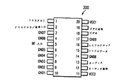
図2は、本発明の集積回路の好適具体例のピンレイアウト図を示している。集積回路200は、ピン11及び20上の供給電圧(VCC1及びVCC2)に接続され、かつピン3、4、6−10、14及び17(GND1−GND9)で接地されている。外部クリスタル発振器からの入力基準信号は、ピン1及びピン2(クリスタル1)及び(クリスタル2/基準IN)上に供給される。集積回路200は、ピン16(シリアルクロック)及びピン15(シリアルデータ)上のIIC(I2 C)インターフェースバスに接続されている。アンテナ又は他のソースからRF入力は、ピン5(RF入力)に接続されている。集積回路200は、ピン18及び19(ビデオ及びビデオ基準)及びピン12及び13(オーディオ及びオーディオ基準)上にビデオ及びオーディオ信号を出力する。
【0045】
図4は、本発明の好適具体例のTVチューナーの詳細電気ブロック図である。図4は、上昇変換二重変換スーパーヘトロダイン受信機を示している。残留側波帯(VSB)コード化ビデオ信号は、検波の前にナイキストスロープ受信機減衰特性フィルタを通して処理される。
【0046】
RF信号は、アンテナ402(又は図示しないケーブル)からTVチューナー100に入り、かつ900MHz以下に入来帯域を制限するようにRF低域フィルタ(RFLPF)404に通される。濾波されたRF信号は、利得制御低ノイズ相互コンダクタンス増幅器(LNTA)406により20dBにまで増幅される。
【0047】
アンテナ402により受信され、RFLPF404により濾波され、かつLNTA406により増幅された入力信号は、標準放送テレビスペクトラムである。VHF帯域におけるチャンネル2−13は54MHzから216MHzにまで延び、かつUHF帯域におけるチャンネル14−83は、470MHzから890MHzにまで延びる。VHF及びUHF帯域における各チャンネルは、6MHzの帯域幅を有し、ビデオキャリア周波数は帯域下縁より上方1.25MHzに位置し、カラーキャリア周波数はビデオキャリア上方3.58MHzに位置し、かつオーディオキャリア周波数はビデオキャリア上方4.5MHzに位置している。例えば、チャンネル2は54〜60MHzの6MHzの帯域幅、55.25MHzのビデオキャリア、58.83MHzのカラーサブキャリア及び59.75MHzのオーディオキャリアを有している。
【0048】
1200と2100MHzの間で動作する第一のローカル発振器(LO1)450の出力は、第一のミキサ(MIX1)408において、RF信号と混合されて、1200MHzの第一のIFビデオキャリア周波数を発生する。これにより、ミキサイメージ及び高調波混合によるひずみが最小になる。第一のIFは、第一のミキサ408の帯域幅制限により濾波されて、高調波影響を最小化する。
【0049】
基本的ミキサスキームにおいて、ミキサは2つの入力、RF入力及びローカル発振器(LO)入力を受信し、かつIF出力を発生する。RF入力は次の一般形を有している。

周波数領域において、IF周波数は、fIF=|fRF±fLO|によって与えられる。実現可能のミキサにおいて、RF及びIF周波数の倍数で高調波を発生する種々の非線形性がある。このように、IFスペクトラムは、fIF=mfRF±nfLOの高調波を包含し、かつここで、m及びnは整数である。
【0051】
例えば、もしローカル発振器450の出力が400MHzであり、かつアンテナから復調されるべき所望の入力信号が800MHzであるならば、基本ミキサは、ミキサ408の出力で1200MHz出力を得るために加算混合を実行するであろう。しかしながら、周波数シンセサイザ450はまた800MHzに高調波を有し、かつ400MHzの信号がアンテナに存在するので、これらの信号はまた付加されて、800MHzで復調されるべき所望の信号を妨害する800MHz出力を発生する。
【0052】
ミキサ408は、RFLPF404によって濾波される0Hz〜900MHzの間の入力RFスペクトラムからローカル発振器450の周波数を減算する減算ミキサである。例えば、RF入力内の復調されるべき所望の周波数が400MHzであるならば、ローカル発振器は1600MHzにセットされ、基本ミキサは2つのIF出力を発生するであろう。
[4]fIF=|400−1600|=1200MHz 及び
[5]fIF=|400+1600|=2000MHz
ミキサ408は減算ミキサであるので、2000MHz信号は濾波されて、1200MHz信号のみがミキサ410に通される。また、ミキサ408は減算ミキサであるので、入来スペクトラムは出力で反転され、そのため、ビデオキャリアは6MHzチャンネル帯域幅の上縁よりも1.25MHz下方であり、カラーキャリアはビデオキャリア以下3.58MHzであり、そしてオーディオキャリアはビデオキャリアの4.5MHz下にある。例えば、54〜60MHzのチャンネル2の6MHzの帯域幅は、1201.25MHzと1195.25MHzの間で反転して現れるであろう。チャンネル2ビデオキャリアは1200MHzに現れ、カラーキャリアは1196.42MHzに現れ、そしてオーディオキャリアは1195.5MHzに現れるであろう。
【0053】
前述したように、高調波信号が所望の周波数の倍数に存在するというのが、LNTA406からミキサ408により受信した入力RF信号と周波数シンセサイザ405の両方の特徴である。減算ミキサ及び発振器450からの十分高い周波数の出力を使用することにより、周波数シンセサイザ450の出力上の高調波は、アンテナ402からの0MHz〜900MHz範囲に存在する入力周波数のいずれよりも1200MHz以上周波数が高い。
【0054】
例えば、ローカル発振器450の最低出力は1200MHzである。この信号の第一の高調波は2400MHzに存在する。LNTA406を通過する最高出力信号は900MHzであるので、2400MHz高調波とアンテナ402からの900MHz信号の減算混合は、|900−1200|=1300MHzの信号を生じるであろう。これは、ミキサ408からの所望の1200MHz出力よりも高く、それ故、ローパスフィルタにより濾波除去することができる。RF入力周波数よりも高い出力のローカル発振器を使うことは、ハイサイドインジェクションとして公知である。
【0055】
1200MHzの第一のIF信号は、イメージ排除ミキサである第二のミキサ(MIX2)410において、第二のローカル発振器(LO2)412の固定1180MHz基準出力と混合されて、20MHz画像キャリアで第二のIFを発生する。RF入力信号がLO基準よりも周波数が低いので、2つの信号の混合によりRF入力の下方変換を生じるであろう。fIF=|fRF±fLO|によって与えられるIF周波数は、fIF=1200−1180=20MHz及びfIF=1200+1180=2380MHzにキャリアを有している。イメージ排除ミキサは特に、fIF=|1160−1180|=20MHzで不所望の信号を生じる1160MHzのエリアにある第一のIF信号において信号エネルギーを排除する。
【0056】
イメージ排除ミキサは、次の一般形を有するMIX1から入力信号を受信する。
[6]VRF=Acos ( ωRFt)
LO2からのローカル発振器信号は、次の一般形を有する2つの位相直交信号に分割される。
[7]VLOI =Bcos ( ωLOt)
[8]VLOQ =Bsin ( ωLOt)
RF入力と位相直交信号の混合から生じる所望の出力信号、VIFは、次の一般形を有している。
[9]VIF=ABcos ( ωRF−ωLO)t
ωIF=ωRF−ωLOの所望のミキサ信号はミキサ出力に現れる一方、ωIF=ωRF+ωLO(−1160+1180=20)の不所望のミキサイメージ信号は排除される。
【0057】
図5は、本発明のRFフロントエンド(即ち、RFコンバータ110及びIFプロセッサ120)の別の具体例を示している。ミキサ408とミキサ510の間の第一のIFフィルタ(FIFF)509は、1160MHzになるイメージの全ての周波数成分を濾波除去して、ミキサ510はイメージ排除ミキサというよりもむしろミキサ408と同様な基本ミキサであるようにする。イメージ排除ミキサは集積するのは容易であるけれども、精度に限界があり、かつノイズ及びひずみを受けるかもしれない。
【0058】
図4に戻ると、第二のIF信号が次に、第二のIFフィルタ(SIFF)420、低ひずみ連続時間バンドパスフィルタにより、最終ビデオ帯域幅のために濾波される。SIFF420はまた、VSB平衡のための自動同調ローパスナイキストスロープフィルタ(NSF)から構成される。NSFのスロープ上の−6dB点は、画像キャリア周波数(20MHz)に維持される。
SIFF420の出力は、80dBの利得まで印加される利得制御増幅器であるIF増幅器(IFAMP)422に結合される。それから、IFAMP422の出力は、ビデオ検波器(VDET)426においてビデオキャリアと混合され、かつこれは、ビデオ減算フィルタ(VCEF)425及びビデオキャリアリミッタ(VCLIM)428により減算されて、ベースバンドビデオ出力を発生する。
【0059】
ビデオキャリアは、自動周波数制御(AFC)周波数検出器(DET)440により、AFCREF442からの合成20MHz基準信号と比較されて、自動周波数制御のためLO1に戻される周波数エラー信号を発生する。
【0060】
VDET426からのベースバンドビデオはローパスビデオ帯域幅フィルタ(VBBF)430に通されて、検波高調波を取り除く。同期化パルスは同期クランプ(SCMP)432により基準レベルにクランプされ、かつこれは、クランプタイミングを制御するために、水平同期速度,”RXLOCK”に、或いは選択として垂直速度にロックされている位相ロックループを包含している。タイミングはまた、AGC438及びNINV436のためのSCMP432において発生する。SCMP432はそのビデオを20dBの固定利得によってその出力電圧レベルに増幅する。クランプされたビデオはノイズインバータ(NINV)436により処理されて、過度に大きな正又は負の振幅ノイズパルスを取り除く。
【0061】
その結果生じるビデオは、AGC438により同期レベルにブランキングするためにテストされ、かつこれは、LNTA406及びIFAMP422の利得を調整して、標準1ボルトピークーツウーピークビデオ信号を維持する。この段階のビデオは、3つの信号インピーダンス標準の1つを使ってチップ外駆動するためにビデオバッファ(BVUF)437によりバッファされる。VBUF437はまたこの信号をミュートすることができる。
【0062】
オーディオ処理は、狭帯域オーディオIFフィルタ(AIFF)427を通してIFAMP422の出力のオーディオ信号を抽出することにより達成される。AIFF427は、AMノイズ及びひずみを除去するためにオーディオIFリミッタ(AIFLIM)444により制限されるFM信号を発生する。
【0063】
オーディオ位相検波器(APD)455、オーディオ遅延ロックループ低域フィルタ(ADLPF)458、及びオーディオ位相シフタ(APS)460から構成される遅延ロックループは、FMキャリア周波数で90°だけ遅延される信号を発生し、かつその信号を、FMの直交検波のためにオーディオ直交検波器(AQD)においてリミッタを通ったFM信号と混合する。オーディオベースバンドは120kHz低域オーディオベースバンドフィルタ(ABF)464に通されて、検波合成成分を除去する。オーディオは,0.35ボルト(rms)レベルで選択可能の駆動インピーダンスで、チップ外駆動するためにオーディオバッファ(ABUF)466においてバッファされる。
【0064】
制御レジスタ471及びステータスレジスタ472は、シリアルディジタルインターフェース170にインターフェースされる。次に、シリアルディジタルインターフェース170は、”シリアルデータ”及び”シリアルクロック”制御ラインを通して外部マイクロプロセッサ又はマイクロコントローラから外部コマンドを受信する。本発明の好適具体例において、シリアルディジタルインターフェース170は、フィリップスコーポレーションの専用仕様であるインター集積回路(IIC又はI2 C)インターフェースにすることができる。
【0065】
システムブロック仕様
TVチューナー100の全体設計は、集積回路上に信頼性良く設計することのできる制限により支配される。TVチューナー100のブロックは、ノイズ、最大信号処理、相互変調、及び利得のような能力を確実にすることができるように、実際の回路要素を参照することにより規定される。たぶん、このような設計の最も重要な要素は、それが高生産高で、それ故低コストで製造することができるように、予期されたチップ性能を制限することである。dBm での全ての測定は、標準ビデオRF及び75オームのベースバンドインピーダンスを基準としているということに注意されたい。
【0066】
RF低域フィルタ(RFLPF)
表1は、本発明の好適具体例のRF低域フィルタ(RFLPF)404の動作パラメータをリストにしている。RFLPF404は、パッケージリードインダクタンス、プリント回路キャパシタンス及びオンチップキャパシタからなる900MHz3次ローパスフィルタである。大部分の用途に対して、RFLPF404は、MIX1におけるイメージ(2400−3300MHz)排除のために満足のいくものである。75オームインピーダンスに合致した外部フィルタを、非常に大きな帯域外信号のような極端な状況に対して付加することができるであろう。
低ノイズ相互コンダクタンス増幅器(LNTA)
表2は、本発明の好適具体例の低ノイズ相互コンダクタンス増幅器(LNTA)406の動作パラメータのリストである。LNTA406は受信機のフロントエンドである。単一端入力信号は、ミキサチエーンに通される差動電流に変換される。この回路の重大な機能は、非常に低いノイズ数値(NF)、相当の利得(GV )、及び高い3次相互変調抑圧(IP3 )を維持することである。この利得は、このブロックのノイズ数値が全受信機ノイズ数値を決定するように、この回路の残りに関して決定される。これは相互コンダクタンス増幅器であるので、利得は、最終ミキサ段の負荷インピーダンスにより限定され、かつLNTA406性能の最終決定前に適切に限定されなければならない。AGC能力は、高レベル信号の存在下で、相互変調又はクロス変調のようなひずみの影響を減少させるために備えられている。この入力は、75オームにマッチさせたインピーダンスである。
第一のミキサ(MIX1)
表3は、本発明の好適具体例の第一のミキサ(MIX1)408の動作パラメータのリストである。ローカル発振器高調波による不所望のイメージ及び偽信号の適切な排除は、MIX1がハイサイドインジェクションを持つ上方変換スキームのために構成されることを必要とする。このように、画像キャリアのためのMIX1の出力は、1200MHzのマイクロウエーブ周波数にあり、オーディオキャリアは1195.5MHzにあり、そしてローカル発振器450の入力は、1.2と2.1GHzの間にある。単極ローパス要素がMIX1の出力回路内に組み込まれて、ローカル発振器高調波による下方変換信号の排除を助ける。MIX1のノイズ及びひずみ影響は、LNTA406仕様内に包含されている。この設計は、必要ならばミキサの出力でいかなるイメージエネルギーもさらに帯域制限するようにボンドワイヤパラレルLC回路網を選択として包含するであろう。
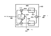
第二のミキサ(MIX2)
表4は、本発明の好適具体例の第二のミキサ(MIX2)の動作パラメータのリストである。1.2GHzの第一のIF(画像キャリア)は、20MHzの第二のIFに下方変換するイメージ排除ミキサであるMIX2に入力される。このイメージ排除は、もしMIX2が普通の減算ミキサであったならばMIX2により下方変換されることから1160MHzのイメージに入る信号を排除するために第一のミキサ出力の濾波の必要性を打ち消すためになされる。MIX2の重要な特徴は、それが、MIX2を校正する製造後トリミング技術の必要性もなく、高いイメージ排除(少なくとも50dB)を達成しなければならないということである。図6に示されるように、50dBイメージ排除は、MIX2入力で2つのギルバートセル乗算器を並列にし、かつ20MHz帯域幅に渡り0.2度以下の位相エラーを加算器615に生じる非常に低い成分感度のかなり高次の平衡RC位相シフタ613、614を使うことにより達成することができる。これらは伝統的に、比較的に高いノイズレベルにより避けられるが、しかし、TVチューナー100の好適具体例において、この前段はノイズ影響を減らすために十分な利得を提供する。
第二のIFフィルタ(SIFF)
表5は、本発明の好適具体例の第二のIFフィルタ(SIFF)420の動作パラメータのリストである。20MHzIF信号は、この集積化相互コンダクタ−キャパシタ(Gm −C)フィルタにおけるチャンネル帯域幅のために濾波される。遷移ガウシアンバンドパスフィルタは、隣接チャンネル及びノイズ排除をするために使用される。SIFF420は、ノイズ及び帯域外信号によるひずみを−54dBc以下に維持する。インチャンネルグループ遅延は、カラーサブキャリア周波数に最大限に平らにすることができる。音声信号は、SIFF420を通過する。上方変換スキームは、MIX2の出力でチャンネル周波数を反転するので、画像キャリアは今20MHzであり、かつ音声キャリアは15.5MHzにある。隣接画像キャリアは今14MHzにあり、かつ隣接音声キャリアは21.5MHzにあり、以下のフィルタ仕様の通りである。
IF増幅器(IFAMP)
表6は、本発明の好適具体例のIF増幅器(IFAMP)の動作パラメータのリストである。20MHz信号がこのブロックにおいて80dB増幅される。この利得は、自動利得制御(AGC)信号電圧の印加により0dBに減少させることができる。このAGCは、最良のオンチップノイズ排除のために完全差動形態で実施される。
画像キャリア抽出フィルタ(VCFF)
表7は、本発明の好適具体例の画像キャリア抽出フィルタ(VCFF)425の動作パラメータのリストである。15MHzのビデオキャリアは同期検波処理のためにIFAMP422出力から抽出される。VCEF425は、最良の検波器性能のためにいかなるグループ遅延ひずみもなくナイキストフィルタにおけるいかなる付随キャリア位相変調(ICPM)も伝達する。
画像キャリアリミッタ(VCLIM)
表8は、本発明の好適具体例の画像キャリアリミッタ(VCLIM)428の動作パラメータのリストである。同期検波器は固定振幅基準キャリアを必要とする。これは、VCEF425を通して得られ、かつそれから、VCLIM428に通される。20dBの入力レベル変動及び95パーセントを超える可能性のある変調深さにより、VCLIM428出力は、−50dBの精度内で安定している。VCEF425とVCLIM428の組み合わされた回路遅延は、検波器出力レベル及びノイズ振る舞いが退化しないように、画像キャリア周波数で45°を超えてはならない。
ビデオ検波器(VDET)
表9は、本発明の好適具体例のビデオ検波器(VDET)426の動作パラメータのリストである。ビデオは、二重平衡ミキサ(VDET426)に第一の入力信号としてIFAMP422の出力を、かつ第二の入力信号としてVCLIM428の出力を印加することにより同期検波される。VDET426の出力は、0.5dB損失で4.2MHzを通過させるようにセットされた低域単一極に構成される。
ビデオベースバンドフィルタ(VBBF)
表10は、本発明の好適具体例のビデオベースバンドフィルタ(VBBF)430の動作パラメータのリストである。検波されたビデオは、SIFF420応答とFCC規則に合致するグループ遅延特性の両方の補償のために予め歪まされた多極遷移ガウシアン応答ローパスフィルタにより4.2MHzに帯域制限されている。VBBF430は、最小通過帯域過渡ひずみでVDET426の出力で、20MHzのビデオキャリア及び高レベル40MHz変調信号を排除する。
同期クランプ(SCMP)
表11は、本発明の好適具体例の同期クランプ(SCMP)432の動作パラメータのリストである。同期パルスは、2つの技術を通してクランプされる。ダイオードクランプは、同期チップがセットされる最小レベルを限定する。いったんこれが達成されると、1同期パルス後、同期スライサが同期パルスのみを再生し、かつこれらを位相ロックループ(PLL)に通過させる。PLLは、水平同期速度を得て、そして水平同期パルス内にほぼ中心のある同期ゲートパルスを発生する。
【0077】
いったんPLLがロックされると、同期ゲートパルスを使うゲート化クランプ回路は同期レベルを限定するようにイネーブルにされて、かつダイオードクランプが不能(ディスエーブル)にされる。スクランブル化ビデオの処理のために、ラインカウンタがフィールドを計数するために位相ロックループ内に挿入され、その同期信号が垂直同期の検出のために積分され、そして垂直同期パルスのみがクランプゲートのために使用される。同期ゲートパルスは、AGC処理のために使用されるブランキングゲートを発生するために5マイクロ秒のクロック化遅延を通して使用される。SCMP432はまた、ビデオをその最終出力レベルに増幅する。出力信号”RXLOCK”434は、位相ロックループが同期パルスにロックしたときアクティブになる。
ノイズインバータ(NINV)
表12は、本発明の好適具体例のノイズインバータ(NINV)436の動作パラメータのリストである。SCMP432ビデオ出力は、黒及び白の両方向に極めて過渡的なノイズパルスを包含するであろう。黒ノイズは典型的には、ある形態の干渉による大きなRF過渡パルスである。この信号は、水平ライン映像周期の間ブランキングレベル以下に降下し、そして、下流の同期検出回路を混乱させるかもしれない。比較器が、映像アクティブの間、或いは非ブランク周期の間、ブランキングレベル以下のこれらのレベルを検出し、そしてオリジナルなビデオと加算される間反転ビデオ路を可能にする。この加算は、同期レベル領域が乱されないようにノイズパルスの影響を打ち消す。白として現れる極端な正方向偏位はまた、それらが108IRE白に等価なレベルを超えるとき、或いは5パーセント変調以下の時打ち消される。これらは典型的には、パルス干渉が帯域外周波数に存在するとき受信機の感度減少降下によるものであり、そして典型的には同期検波器の遮断を生じる。108IREレベルを基準とする比較器を使い、かつ上述の負の場合のように加算器へのビデオ反転路を可能にする正のノイズ反転が達成される。
自動利得制御(AGC)
表13は、本発明の好適具体例の自動利得制御(AGC)438の動作パラメータのリストである。クランプされたビデオは、ブランキングゲートにより制御されるサンプルアンドホールド回路に導かれる。サンプルアンドホールド回路出力は、標準NTSCビデオ波形のための所望の出力ブランキングレベルに等しい基準レベルを他の入力に有する差動増幅器を駆動する。
【0080】
各水平同期パルスで、差動増幅器の出力は、ビデオ波形を達成するための受信機の利得エラーを表している。これは、必要なとき利得を調整するためにLNTA406及びIFAMP422にフィードバックされる。差動増幅器のタイミング及び利得は、航空機誘起動揺(フェージング)の償いをする高速過渡応答時間及び絶対的な安定性に対して設定されなければならない。この応答は、SCMP432によるように垂直同期期間のみ利得を更新するために変化させることができ、そのためスクランブルされたビデオは、いかなる悪影響もなくチューナーを通過させることができる。
【0081】
RF及びIF増幅性能及び入力信号レベルにより限定されるAGC電圧は、4ビットアナログーディジタルコンバータを経て測定され、かつデータワード受信信号強度インディケータ(RSSI)439として記憶される。自動利得制御は、ビデオレベルを減少させるためにIFAMP422に最初に印加され、そしてまた50dB以上減少させて、遅延AGC機能を実施するLNTA406に印加される。
ビデオ出力バッファ(VBUF)
表14は、本発明の好適具体例のビデオバッファ(VBUF)437の動作パラメータのリストである。ビデオは、1ボルトピークツーピーク差の内部レベルである。VBUF437は、負荷抵抗器を駆動する線形相互コンダクタンス増幅器を通してこの信号を電流に変換する。フィードバックは、次の段にAC結合が必要とされないように、増幅器の利得及びオフセットの連続調整を可能にするために外部信号を通して配置される。オンチップ積分器が使用されて、フィードバックレベルを限定し、かつビデオ信号を排除する。制御信号VOUT−MODE445は、電流源出力に等しい75オーム、1000オーム、或いは負荷無しのオンチップ負荷をイネーブルにする。制御信号VIDEO−MUTE446は、ブランキングレベルに出力をセットするビデオミュートスイッチをイネーブルにする。
自動周波数制御(AFC)周波数検出器
表15は、本発明の好適具体例の自動周波数制御(AFC)周波数検出器(DET)440の動作パラメータのリストである。抽出されたIFビデオキャリアは、20MHzの固定基準と比較され、かつ2つを等しくする方向にLO1を駆動するために使用される。周波数制御設定からのLO1におけるエラーが、信号AFC−ERROR452である。20MHz基準が、マスタ基準から周波数シンセサイザーを通して発生する。20MHz基準は、抽出ビデオキャリア信号とVCEF425の出力で、ディジタル周波数比較器を使って比較され、かつこれは、I2 Cインターフェース170からLO1に送られる周波数コードの下位ビットと加算される7ビットアップダウンカウンタを駆動する。このように、周波数エラーは、インターフェースバスを通して読み取ることのできるカウンタに現れる。このカウンタは、周波数エラーがないとき1000000bにセットされる。この条件は、ステータス信号FREQ−LOCK453をセットする。
AFC基準発振器(AFCREF)
表16は、本発明の好適具体例のAFC基準発振器(AFCREF)442の動作パラメータのリストである。AFCREF442は、20MHzで動作する固定周波数シンセサイザーであり、かつこれは、水晶周波数基準に位相ロックされる。位相ノイズは、低変調周波数のみでこの回路に印加されることにより特に重要なものとはならない。
![]()
第一のローカル発振器(LO1)
表17は、本発明の好適具体例の第一のローカル発振器(LO1)450の動作パラメータのリストである。LO1は、過度の偽ノイズ応答もなく最良の受信機感度を可能にするために、特別のレベルの位相ノイズに対して構成された位相ロック周波数シンセサイザーである。それは、ディジタル制御され、かつ水晶周波数基準及びインバンド位相ノイズ制御を利用する。シリアルディジタルインターフェース170バスからの周波数制御入力FREQUENCY451は、62.5kHzLSB分解能を持つ16ビットを有している。最初の3LSBと共にさらに4LSBが精細同調のためにAFCにより使用される。
第二のローカル発振器(LO2)
表18は、本発明の好適具体例の第二のローカル発振器(LO2)412の動作パラメータのリストである。LO2は、1180MHzにセットされた固定同調周波数シンセサイザーである。それは、LO1と同じ周波数基準を使用し、かつ同様な位相ノイズ特性を有している。
オーディオIFフィルタ(AIFF)
表19は、本発明の好適具体例のオーディオIFフィルタ(AIFF)427の動作パラメータのリストである。オーディオIF信号は、IFAMP422の出力からタップされ、かつ300kHzの帯域幅を持ち15.5MHzで動作する狭帯域フィルタを通して動作する。AIFF427は、ビデオキャリア及びバースト周波数成分を排除する。
オーディオIFリミッタ(AIFLIM)
表20は、本発明の好適具体例のオーディオIFリミッタ(AIFLIM)444の動作パラメータのリストである。オーディオIFは、AGC438及び放送信号ソース間の差に基づいた入力レベルの40dBの可能性ある変動でリミットされる。この範囲での出力レベル精度は、−40dBよりも良い。
オーディオ位相検出器(APD)
表21は、本発明の好適具体例のオーディオ位相検出器(APD)455の動作パラメータのリストである。オーディオIFは、遅延ロックループにおいてAPS460を駆動する位相エラー信号を発生するためにAPS460出力と比較される。APD455は、高速ループ捕捉及びいったん捕捉された最小位相のために構成された位相検出器である。
オーディオDLLローバスフィルタ(ADLPF)
表22は、本発明の好適具体例のオーディオ遅延ロックループローパスフィルタ(ADLPF)458の動作パラメータのリストである。ADLPF458は、検出信号における完全なオーディオ帯域幅を達成するために20Hz以上のいかなる周波数にも応答してはならない。このローパスフィルタは、この要求に適合する。
オーディオ位相シフタ(APS)
表23は、本発明の好適具体例のオーディオ位相シフター(APS)の動作パラメータのリストである。APS460は、遅延ロックループを通してオーディオキャリアにロックされる電圧制御位相シフターである。APS460は、15.5MHzの音声キャリア周波数で出力信号に90度の位相シフトを発生する。
オーディオ直交検波器(AQD)
表24は、本発明の好適具体例のオーディオ直交検波器(AQD)462の動作パラメータのリストである。AQD462は、入来オーディオIF信号を、入来キャリアと直交のIF信号の遅延したものと比較するために使用されるミキサーである。この出力は、所望のオーディオベースバンド信号である。
オーディオベースバンドフィルタ(ABF)
表25は、本発明の好適具体例のオーディオベースバンドフィルタ(ABF)464の動作パラメータのリストである。ABF464は、120kHzにカットオフを持つ高次チェビチェブローパスフィルタ設計である。これは、外部デコーディングのために全ての多重オーディオサブキャリアを通過させるのに十分広い。
オーディオ出力バッファ(ABUF)
表26は、本発明の好適具体例のオーディオ出力バッファ(ABUF)466の動作パラメータのリストである。このオーディオは、0.1ボルトピークツーピークの内部レベルにある。ABUF466は、この信号を、負荷抵抗器を駆動する線形相互コンダクタンス増幅器を通して、電流に変換する。次段にいかなるAC結合も必要とされないように、増幅器の利得及びオフセットを連続的に調整可能にするように外部信号を通してフィードバックが配列される。オンチップ積分器が、フィードバックレベルを限定し、かつオーディオ信号を排除するために使用される。
【0095】
制御信号AOUT−MODE467が、電流源出力に等しい600Ω、10kΩ又は無負荷のオンチップ負荷を可能にする。制御信号AUDIO−MUTE468は、出力を不能にするオーディオミュートスイッチを制御する。
シリアルディジタルインターフェース
表27−29は、本発明の好適具体例のシリアルディジタルインターフェース170によりアドレス可能のレジスタ、レジスタビット、及びビット機能を定義する。例えば、制御及びステータスは、インター集積回路(I2 C)バスインターフェースを通して実行することができる。シリアルディジタルインターフェース170は、全てのレジスタを包含し、かつシリアルバスを通して全てのパラレルディジタルオンチップ機能にアクセスを提供する。
各レジスタにおいて使用されるビットの定義は以下の通りである。
ステータスレジスタは読み取り専用である。ステータスレジスタに書込を試みることは無駄である。各ビットの機能は以下に定義される通りである。
バイアス及び制御(BC)
表30は、本発明の好適具体例のバイアス及び制御ロジック(BC)180の動作パラメータのリストである。バイアス電圧及び電流が、本発明の各回路要素のために必要な特別のレベルを限定するために発生する。制御信号POWERDOWN476は、BC180を通してパワーダウン機能を制御する。
本発明及びその利点を詳細に説明したけれども、特許請求の範囲に限定されるような本発明の精神及び範囲から離れることなく、種々の変化、代換え、及び変更がここでなすことができるということが理解されよう。
【0101】
【発明の効果】
(1) 本発明は、プリント回路ボード上で使用するために、比較的に低コストで、かつ小さな物理スペースを持つTVチューナーを提供することができる。
(2) 本発明は、同時に必要とされる外部要素の数を減少させ、それによって、プリント回路ボードの複雑さ、及びTVチューナーによって必要とされる回路ボード面積を減少させつつ、最先端TVチューナーの性能に合致するか或いはそれを超えるTVチューナーを提供することができる。
(3) 本発明は、TVチューナーが、テレビ受像機、パーソナルコンピュータ、又は他のビデオ装置に埋め込まれたマイクロコントローラにより制御することができるように、シリアルバスによりTVチューナーのコンピュータ制御を可能にすることができる。
(4) 本発明は、コンピュータ制御出力インピーダンス特性を、異なる負荷仕様に適応させるTVチューナーを提供することができる。
【図面の簡単な説明】
【図1】本発明の機能要素の高レベルブロック図である。
【図2】本発明の集積回路のピンレイアウト図である。
【図3】従来技術に見られる現在のテレビチューナーの詳細なブロック図である。
【図4】本発明の回路要素の詳細なブロック図である。
【図5】本発明のRFフロントエンドの別の具体例を示している。
【図6】図4のMIX2の詳細なブロック図である。
【符号の説明】
100 TVチューナー
110 RFコンバータ
120 IFプロセッサ
130 VSBビデオ検波器
140 FMオーディオ検波器
150 ビデオプロセッサ及びドライバ
160 オーディオプロセッサ及びドライバ
170 シリアルディジタルインターフェース
180 バイアス及び制御
190 周波数基準[0001]
BACKGROUND OF THE INVENTION
The present invention relates to television tuner circuits, and more particularly to highly integrated television tuners assembled in a single microcircuit device.
[0002]
[Prior art]
One of the most important costs in television production is the cost of the tuner. The typical cost of a television (TV) tuner is about $ 15,000, which is significant relative to the overall cost of the television receiver. One solution to reduce tuner cost is to reduce the number of parts in the tuner.
[0003]
Traditionally, a tuner is composed of two basic elements. The first element performs high frequency intermediate frequency conversion (RF to IF). A second element then converts the IF to baseband. TV tuners were originally designed to receive television broadcasts within a television receiver, which is essentially a stand-alone unit that includes a cathode ray tube. As such, TV tuners were originally integrated components embedded in single-purpose devices.
[0004]
However, currently, state-of-the-art consumer electronic devices use TV tuners that are not built-in parts of television receivers. The tuner is a separation element that is connected in some way to the cathode ray tube, but the tuner is not an integral part of the monitor. For example, a TV tuner can be assembled on a circuit board and then attached to a personal computer (PC) system so that the PC functions as a television receiver. These tuners convert radio frequency television signals into baseband (or low frequency) video signals that can then be transmitted to other elements in the PC for video processing applications.
[0005]
A circuit element that performs RF-to-IF conversion typically consists of one or two integrated circuits and a number of individual elements--inductors, capacitors, and / or transistors. IF-to-baseband conversion typically involves another integrated circuit, several filter elements such as ceramic filters and SAW filters, a series of tuning and control elements such as resistors and potentiometers, variable inductors and / or Or a capacitor and some additional external elements. Thus, the complexity of the tuner is quite high and typically there are 100 to 200 elements on the circuit board. Furthermore, state-of-the-art TV tuners still need to be adjusted by manual tuning before each tuner leaves the factory. This manual tuning is one of the most expensive costs associated with the manufacturing process and is an important factor in tuner cost.
[0006]
Past broadcast television tuners have been developed for over 60 years. The earliest tuners utilized vacuum tube technology and required the use of a minimum number of tubes due to their cost, power consumption and size. Therefore, passive elements such as resistors, capacitors, inductors and transistors were used as much as possible in most designs. This design style continued until around 1960, when TV tuner elements, especially vacuum tubes, began to be replaced by bipolar and MOS transistors. However, the total number of active elements has continued to limit the cost and size of TV tuners and minimize the total number of active elements.
[0007]
In the early 1970s, integrated circuits became practical as an element in television tuners, and their design techniques changed dramatically. Many functions of a tuner that uses only one tube or transistor are replaced with 4-20 individual transistors, and this is accurate, small space, low power, low heat generation and cost Will be able to perform the same function. The introduction of integrated circuits was modest, initially only low frequency elements and then extended to high frequency active elements. Nevertheless, many active elements outside the integrated circuit remained in the TV tuner design.
[0008]
With one advance, SAW (Surface Acoustic Wave) filters, there is considerable change, some manually tuned inductors and capacitors are removed from the tuner, and the receive filter performance is in a much smaller space and with reduced cost I was able to improve. However, SAW filters assembled on ceramic substrates cannot be integrated on a silicon wafer with the rest of the active circuitry, and therefore individual elements must remain in the final design. The trend in the 1980s was to make all of the passive elements small and simplify their associated manual tuning at the factory. Recently, TV tuners have been reduced in size from a fairly large case of about 2 "x 5" x 1 "to a much smaller case of about 1/2" x 2 "x 3/8". Because TV tuners are used in increasingly smaller computers, television receivers, and VCRs, they are respected by small size and high respect. Since the device in which the tuner is used becomes smaller, the size of the TV tuner must also be reduced. As the tuner size decreases and as the tuner is used in a variety of devices, the cost becomes more significant and must be reduced as much as possible so that it does not occupy a large portion of the final product cost. When a tuner is used in a television receiver, the size of the tuner is less important because the television receiver has an inherently large volume. However, when the tuner is used in other electronic devices, the space becomes large and the tuner's physical space becomes significant.
[0009]
Before describing the monolithic TV tuner of the present invention, it would be useful to describe the state-of-the-art TV tuner found in the prior art.
[0010]
Although there has been a theoretical proposal to integrate a TV tuner in a single microcircuit, what has been realized is not known. The next best known prior art is very miniaturized, but not a fully integrated tuner as shown in FIG.
[0011]
FIG. 3 shows a functional electrical block diagram of a state-of-the-art TV tuner configuration. The
[0012]
The prior
[0013]
The
[0014]
The output of the
[0015]
The output of the bandpass and image
[0016]
The
[0017]
The 45.75 MHz output signal of the
[0018]
The output of the
[0019]
The output of
[0020]
The
[0021]
The output of the
The output of the
[0022]
The audio signal is an FM signal that passes through the
[0023]
Baseband and image
[0024]
[Problems to be solved by the invention]
Accordingly, one object of the present invention is to provide a TV tuner that is relatively low cost and has a small physical space for use on a printed circuit board.
[0025]
Another object of the present invention is to reduce the number of external elements required at the same time, thereby reducing the complexity of the printed circuit board and the circuit board area required by the TV tuner, while maintaining the state-of-the-art TV. It is to provide a TV tuner that meets or exceeds the performance of the tuner.
[0026]
Yet another object of the present invention is to allow computer control of the TV tuner via a serial bus so that the TV tuner can be controlled by a microcontroller embedded in a television set, personal computer, or other video device. Is to do.
[0027]
Yet another object of the present invention is to provide a TV tuner that adapts computer controlled output impedance characteristics to different load specifications.
[0028]
[Means for Solving the Problems]
These and other problems have been solved by integrating a TV tuner that takes a wideband frequency as input and demodulates video over a very narrow bandwidth. To achieve this, one architecture has been chosen that upconverts the RF input signal to a higher internal frequency, and this allows the filtering at the receiver input stage to be minimized according to the present invention. did. Therefore, the present invention can operate without a variable tuning filter on the input, except for a single fixed tuning filter. This eliminates the need for precision controlled tunable filters that need to be mechanically adjusted during manufacture and that are subject to performance variations due to age, temperature, humidity, vibration and power performance. This, along with complexity, was a serious flaw in conventional tuners that had to be eliminated because it was a source of large errors and distortions.
[0029]
Further, by removing the input or output of the high frequency signal to the integrated circuit of the present invention, the drive capability problem associated with the high frequency signal and the noise coupling problem associated with the external interconnection of the integrated circuit can be avoided. It is advantageous to perform the up-conversion above. The present invention then downconverts from high frequencies using an image exclusion mixing scheme that provides a tightly controlled downconversion that adds little distortion. This further minimizes the on-chip filtering effect by minimizing the amount of filtering that must be done at high frequencies. As a result, the high frequency operation of the present invention is limited to the initial stage inside the chip and is performed at a very low impedance level to minimize distortion. After down conversion, all remaining filtering is performed with a continuous time mode filter implemented in an integrated circuit.
[0030]
Another technical advantage of the present invention is that manual tuning of the final design is not required. As existing in the prior art, no external elements are required to perform the adjustment.
[0031]
Yet another technical advantage of the present invention is that the output impedance can be selected based on system requirements, thereby minimizing power consumption for a particular application. The present invention can drive a coaxial cable with a low output impedance driver, or for board level applications, the present invention can be configured to drive a high output impedance. The present invention can also be matched to a very accurate load impedance limited by a single external element.
[0032]
The present invention advantageously uses much less board space than conventional designs (on the order of 5% to 10% of prior art designs) and consumes only about 1/5 of the power. The present invention also advantageously operates at a single voltage level over two or three voltage levels of conventional design.
[0033]
Another technical advantage of the present invention is that the need for a metal case is reduced. The integration itself allows sufficient shielding to meet interference criteria. The monolithic television (MTV) tuner embodied in the present invention is intended to replace the TV tuner module currently used in most television broadcast receivers. The MTV tuner integrates all of the functional elements of the tuner except for the crystal frequency reference and the power supply bypass capacitor. The level of integration of the present invention dramatically reduces the cost of a basic TV tuner and increases its manufacturability and reliability. The TV tuner of the present invention has a digital serial bus interface (I 2 C) is externally controlled by a computer or a controller. The preferred embodiment of the present invention provides an antenna input that can be connected directly to a standard coaxial cable, thereby enabling both antenna and cable television applications. In addition, baseband video and audio outputs are designed for high impedance or low impedance applications. The high impedance mode is a driver for short interconnections on the printed circuit and provides the benefits of low operating power. Low impedance mode drives an industry standard studio cable interface that requires a larger power supply.
[0034]
The preferred embodiment of the present invention is designed to operate at frequencies used for both aerial and cable television by National Television Standards Committee (NTSC) coded video. The receiver sensitivity is set to be limited by the antenna noise temperature for the VHF system. The present invention also uses extensive automatic gain control (AGC).
[0035]
The baseband video output of the present invention is stabilized, i.e., minimizes video amplitude variations with respect to antenna RF signal level, and softer for either low impedance studio standard loads or high impedance loads at lower operating currents. It can be configured through wear. The audio output is wideband hybrid to connect to an external MTS decoder. The audio output can be configured for low impedance studio standard loads or high impedance loads through software control.
[0036]
I 2 Control is achieved through the C-bus interface. The bias and control circuit in the preferred embodiment of the present invention is an internal register that can be updated through a control bus for operating frequencies, video and audio transmission standards, power, and test modes such as NTSC, PAL, SECAM and MTS. Is included. The status of the bias and control circuit is I 2 It can be checked via a status register accessible through the C bus interface. Status data includes AFC errors, channel locks and received signal strength indicators.
[0037]
The operating frequency of the present invention is referenced to an external crystal or reference frequency generator. According to the present invention, minimal external elements are used and no adjustment of any elements is required.
[0038]
The present invention can be implemented in a bipolar, BiCMOS or CMOS process, however, the preferred embodiment of the present invention uses the BiCMOS process to maximize flexibility and reduce design difficulties. Let
[0039]
The preferred embodiment of the present invention performs sound processing after IF amplification and before video demodulation. This method is known as “quasi-split” sound and is not used in most television receivers for cost reasons. Quasi-split sound does not have a “buzz” sound in the audio signal while the video image is completely white. In the integrated circuit of the present invention, quasi-split sound is negligibly low in cost and can therefore be integrated in all embodiments of the present invention. The accumulation of quasi-split sound reduces the total number of elements and does not require external manual adjustment.
[0040]
The foregoing has outlined rather broadly the features and technical advantages of the present invention in order that the detailed description of the integrated television tuner that follows may be better understood. Additional features and advantages of the monolithic television tuner that form the subject of the claims of the present invention are described below. Those skilled in the art will recognize that the disclosed concepts and specific examples can be readily utilized as a basis for designing modifications or other configurations to accomplish the same objectives of the present invention. . Also, those skilled in the art will recognize that such equivalent constructions do not depart from the spirit and scope of the invention as set forth in the claims.
[0041]
DETAILED DESCRIPTION OF THE INVENTION
For a more complete understanding of the present invention and its advantages, reference is now made to the following description taken in conjunction with the accompanying drawings.
[0042]
FIG. 1 shows a high level block diagram of the functional elements included in a preferred embodiment of the
[0043]
The output of
[0044]
FIG. 2 shows a pin layout diagram of a preferred embodiment of the integrated circuit of the present invention.
[0045]
FIG. 4 is a detailed electrical block diagram of the TV tuner of the preferred embodiment of the present invention. FIG. 4 shows an up-converting double conversion superheterodyne receiver. The residual sideband (VSB) coded video signal is processed through a Nyquist slope receiver attenuation characteristic filter prior to detection.
[0046]
The RF signal enters the
[0047]
The input signal received by
[0048]
The output of a first local oscillator (LO1) 450 operating between 1200 and 2100 MHz is mixed with an RF signal in a first mixer (MIX1) 408 to generate a first IF video carrier frequency of 1200 MHz. . This minimizes distortion due to the mixer image and harmonic mixing. The first IF is filtered by the bandwidth limitation of the
[0049]
In the basic mixer scheme, the mixer receives two inputs, an RF input and a local oscillator (LO) input, and generates an IF output. The RF input has the following general form:
In the frequency domain, the IF frequency is f IF = | F RF ± f LO Is given by |. In feasible mixers, there are various nonlinearities that generate harmonics at multiples of the RF and IF frequencies. Thus, the IF spectrum is f IF = Mf RF ± nf LO And where m and n are integers.
[0051]
For example, if the output of the
[0052]
The
[4] f IF = | 400-1600 | = 1200 MHz and
[5] f IF = | 400 + 1600 | = 2000MHz
Since
[0053]
As described above, it is a feature of both the input RF signal received by the
[0054]
For example, the minimum output of the
[0055]
The first IF signal of 1200 MHz is mixed with the fixed 1180 MHz reference output of the second local oscillator (LO2) 412 in the second mixer (MIX2) 410, which is an image rejection mixer, and the second IF on the 20 MHz image carrier. Generate IF. Since the RF input signal is lower in frequency than the LO reference, mixing the two signals will result in a down conversion of the RF input. f IF = | F RF ± f LO The IF frequency given by | IF = 1200-1180 = 20 MHz and f IF = 1200 + 1180 = 2380 MHz with carrier. The image rejection mixer is especially f IF = | 1160-1180 | = Eliminate signal energy in the first IF signal in the 1160 MHz area that produces unwanted signals at 20 MHz.
[0056]
The image rejection mixer receives an input signal from
[6] V RF = Acos (ω RF t)
The local oscillator signal from LO2 is split into two phase quadrature signals having the following general form:
[7] V LOI = Bcos (ω LO t)
[8] V LOQ = Bsin (ω LO t)
Desired output signal resulting from mixing RF input and phase quadrature signal, V IF Has the following general form:
[9] V IF = ABcos (ω RF −ω LO ) T
ω IF = Ω RF −ω LO While the desired mixer signal appears at the mixer output, IF = Ω RF + Ω LO Undesired mixer image signals of (−1160 + 1180 = 20) are eliminated.
[0057]
FIG. 5 shows another embodiment of the RF front end (ie,
[0058]
Returning to FIG. 4, the second IF signal is then filtered for the final video bandwidth by a second IF filter (SIFF) 420, a low distortion continuous time bandpass filter.
The output of
[0059]
The video carrier is compared by an automatic frequency control (AFC) frequency detector (DET) 440 with the synthesized 20 MHz reference signal from
[0060]
Baseband video from
[0061]
The resulting video is tested by
[0062]
Audio processing is accomplished by extracting the audio signal at the output of
[0063]
A delay lock loop composed of an audio phase detector (APD) 455, an audio delay lock loop low pass filter (ADLPF) 458, and an audio phase shifter (APS) 460 receives a signal delayed by 90 ° at the FM carrier frequency. And the signal is mixed with an FM signal that has passed through a limiter in an audio quadrature detector (AQD) for FM quadrature detection. The audio baseband is passed through a 120 kHz low frequency audio baseband filter (ABF) 464 to remove the detection synthesis component. Audio is buffered in an audio buffer (ABUF) 466 for off-chip drive with a selectable drive impedance at a 0.35 volt (rms) level.
[0064]
The
[0065]
System block specifications
The overall design of the
[0066]
RF low-pass filter (RFLPF)
Table 1 lists the operating parameters of the RF low pass filter (RFLPF) 404 of the preferred embodiment of the present invention. The
Low noise transconductance amplifier (LNTA)
Table 2 is a list of operating parameters for a low noise transconductance amplifier (LNTA) 406 of the preferred embodiment of the present invention.
First mixer (MIX1)
Table 3 lists the operating parameters of the first mixer (MIX1) 408 of the preferred embodiment of the present invention. Proper elimination of unwanted images and spurious signals due to local oscillator harmonics requires that MIX1 be configured for an up-conversion scheme with high side injection. Thus, the MIX1 output for the image carrier is at a microwave frequency of 1200 MHz, the audio carrier is at 1195.5 MHz, and the input of the
Second mixer (MIX2)
Table 4 is a list of operating parameters of the second mixer (MIX2) of the preferred embodiment of the present invention. The first IF (image carrier) of 1.2 GHz is input to MIX2, which is an image rejection mixer that converts down to a second IF of 20 MHz. This image rejection eliminates the need for filtering the first mixer output to eliminate the signal entering the 1160 MHz image if MIX2 was a normal subtracting mixer and would be down converted by MIX2. Made. An important feature of MIX2 is that it must achieve high image rejection (at least 50 dB) without the need for post-production trimming techniques to calibrate MIX2. As shown in FIG. 6, 50 dB image rejection is a very low component that causes two Gilbert cell multipliers in parallel at the MIX2 input and produces a phase error of less than 0.2 degrees across
Second IF filter (SIFF)
Table 5 is a list of operating parameters of the second IF filter (SIFF) 420 of the preferred embodiment of the present invention. The 20 MHz IF signal is derived from this integrated transconductor-capacitor (G m -C) Filtered for channel bandwidth in the filter. Transition Gaussian bandpass filters are used to eliminate adjacent channels and noise. The
IF amplifier (IFAMP)
Table 6 is a list of operating parameters of the IF amplifier (IFAMP) of the preferred embodiment of the present invention. A 20 MHz signal is amplified by 80 dB in this block. This gain can be reduced to 0 dB by applying an automatic gain control (AGC) signal voltage. This AGC is implemented in fully differential form for best on-chip noise rejection.
Image carrier extraction filter (VCFF)
Table 7 is a list of operating parameters of the image carrier extraction filter (VCFF) 425 of the preferred embodiment of the present invention. A 15 MHz video carrier is extracted from the
Image carrier limiter (VCLIM)
Table 8 is a list of operating parameters of the preferred embodiment image carrier limiter (VCLIM) 428 of the present invention. Synchronous detectors require a fixed amplitude reference carrier. This is obtained through
Video detector (VDET)
Table 9 is a list of operating parameters of the video detector (VDET) 426 of the preferred embodiment of the present invention. The video is synchronously detected by applying the output of
Video baseband filter (VBBF)
Table 10 is a list of operating parameters of the video baseband filter (VBBF) 430 of the preferred embodiment of the present invention. The detected video is band limited to 4.2 MHz by a pre-distorted multipole transition Gaussian response low pass filter to compensate for both the
Synchronous clamp (SCMP)
Table 11 is a list of operating parameters for a preferred embodiment of the present invention synchronous clamp (SCMP) 432. The sync pulse is clamped through two techniques. The diode clamp limits the minimum level at which the sync chip is set. Once this is achieved, after one sync pulse, the sync slicer regenerates only the sync pulses and passes them through a phase locked loop (PLL). The PLL obtains the horizontal sync rate and generates a sync gate pulse that is approximately centered within the horizontal sync pulse.
[0077]
Once the PLL is locked, the gated clamp circuit that uses the sync gate pulse is enabled to limit the sync level and the diode clamp is disabled. For processing scrambled video, a line counter is inserted in the phase lock loop to count the field, its sync signal is integrated for detection of vertical sync, and only the vertical sync pulse is for the clamp gate Used for. The sync gate pulse is used through a 5 microsecond clocking delay to generate the blanking gate used for AGC processing.
Noise inverter (NINV)
Table 12 is a list of operating parameters of the noise inverter (NINV) 436 of the preferred embodiment of the present invention. The
Automatic gain control (AGC)
Table 13 is a list of operating parameters of the automatic gain control (AGC) 438 of the preferred embodiment of the present invention. The clamped video is directed to a sample and hold circuit controlled by a blanking gate. The sample and hold circuit output drives a differential amplifier having a reference level at the other input equal to the desired output blanking level for a standard NTSC video waveform.
[0080]
With each horizontal sync pulse, the output of the differential amplifier represents the gain error of the receiver to achieve the video waveform. This is fed back to
[0081]
The AGC voltage, limited by RF and IF amplification performance and input signal level, is measured via a 4-bit analog to digital converter and stored as a data word received signal strength indicator (RSSI) 439. Automatic gain control is first applied to
Video output buffer (VBUF)
Table 14 is a list of operating parameters of the video buffer (VBUF) 437 of the preferred embodiment of the present invention. The video is an internal level with a 1 volt peak-to-peak difference.
Automatic frequency control (AFC) frequency detector
Table 15 is a list of operating parameters for an automatic frequency control (AFC) frequency detector (DET) 440 of the preferred embodiment of the present invention. The extracted IF video carrier is compared to a fixed reference of 20 MHz and is used to drive LO1 in a direction that makes the two equal. The error in LO1 from the frequency control setting is signal AFC-ERROR452. A 20 MHz reference is generated from the master reference through a frequency synthesizer. The 20 MHz reference is compared at the output of the extracted video carrier signal and
AFC reference oscillator (AFCREF)
Table 16 is a list of operating parameters for the AFC reference oscillator (AFCREF) 442 of the preferred embodiment of the present invention. The
![]()
First local oscillator (LO1)
Table 17 is a list of operating parameters of the first local oscillator (LO1) 450 of the preferred embodiment of the present invention. LO1 is a phase-locked frequency synthesizer that is configured for a special level of phase noise to allow the best receiver sensitivity without excessive spurious noise response. It is digitally controlled and utilizes a crystal frequency reference and in-band phase noise control. The frequency
Second local oscillator (LO2)
Table 18 is a list of operating parameters of the second local oscillator (LO2) 412 of the preferred embodiment of the present invention. LO2 is a fixed tuning frequency synthesizer set at 1180 MHz. It uses the same frequency reference as LO1 and has similar phase noise characteristics.
Audio IF filter (AIFF)
Table 19 lists the operating parameters of the audio IF filter (AIFF) 427 of the preferred embodiment of the present invention. The audio IF signal is tapped from the output of
Audio IF limiter (AIFLIM)
Table 20 is a list of operating parameters of the audio IF limiter (AIFLIM) 444 of the preferred embodiment of the present invention. The audio IF is limited by a 40 dB possible variation in input level based on the difference between
Audio phase detector (APD)
Table 21 is a list of operating parameters of the preferred embodiment audio phase detector (APD) 455 of the present invention. The audio IF is compared to the
Audio DLL low-pass filter (ADLPF)
Table 22 is a list of operating parameters of the audio delay locked loop low pass filter (ADLPF) 458 of the preferred embodiment of the present invention. The
Audio phase shifter (APS)
Table 23 is a list of operating parameters of the audio phase shifter (APS) of the preferred embodiment of the present invention.
Audio quadrature detector (AQD)
Table 24 is a list of operating parameters of the audio quadrature detector (AQD) 462 of the preferred embodiment of the present invention.
Audio baseband filter (ABF)
Table 25 is a list of operating parameters of the audio baseband filter (ABF) 464 of the preferred embodiment of the present invention. ABF 464 is a high order Ceviche blow pass filter design with a cutoff at 120 kHz. This is wide enough to pass all the multiplexed audio subcarriers for outer decoding.
Audio output buffer (ABUF)
Table 26 is a list of operating parameters of the audio output buffer (ABUF) 466 of the preferred embodiment of the present invention. This audio is at an internal level of 0.1 volts peak-to-peak.
[0095]
A control signal AOUT-
Serial digital interface
Tables 27-29 define registers, register bits, and bit functions that are addressable by the serial
The definition of bits used in each register is as follows.
The status register is read-only. Attempting to write to the status register is useless. The function of each bit is as defined below.
Bias and control (BC)
Table 30 is a list of operating parameters of the bias and control logic (BC) 180 of the preferred embodiment of the present invention. Bias voltages and currents are generated to limit the special levels required for each circuit element of the present invention. The
Although the invention and its advantages have been described in detail, various changes, substitutions and alterations can be made herein without departing from the spirit and scope of the invention as limited by the claims. It will be understood.
[0101]
【The invention's effect】
(1) The present invention can provide a TV tuner having a small physical space at a relatively low cost for use on a printed circuit board.
(2) The present invention reduces the number of external elements required at the same time, thereby reducing the complexity of the printed circuit board and the circuit board area required by the TV tuner, while at the same time cutting-edge TV tuners. A TV tuner that meets or exceeds the performance of the TV can be provided.
(3) The present invention enables computer control of the TV tuner via a serial bus so that the TV tuner can be controlled by a microcontroller embedded in a television set, personal computer, or other video device. be able to.
(4) The present invention can provide a TV tuner that adapts computer-controlled output impedance characteristics to different load specifications.
[Brief description of the drawings]
FIG. 1 is a high-level block diagram of functional elements of the present invention.
FIG. 2 is a pin layout diagram of the integrated circuit of the present invention.
FIG. 3 is a detailed block diagram of a current television tuner found in the prior art.
FIG. 4 is a detailed block diagram of the circuit elements of the present invention.
FIG. 5 shows another embodiment of the RF front end of the present invention.
FIG. 6 is a detailed block diagram of
[Explanation of symbols]
100 TV tuner
110 RF converter
120 IF processor
130 VSB video detector
140 FM audio detector
150 Video processor and driver
160 Audio Processor and Driver
170 Serial digital interface
180 Bias and control
190 Frequency reference
Claims (8)
前記第一のミキサーの後段に設けられ、一以上のチャンネルを通過させて、部分的なイメージ除去を行うと共に信号強度を制限する第一のバンドパスフィルタと、
第二の動作周波数を有する第二の基準信号と、前記第一のバンドパスフィルタの出力とに基づいて、第二のIF信号を生成する第二のミキサーと、
が1パッケージのICに集積され、
前記第二のミキサーがイメージ除去ミキサーであることを特徴とするテレビチューナー。 A first mixer that combines a receiver input coupled to an RF signal source and a first reference signal having a first operating frequency to produce a first IF signal ;
Provided after the first mixer, it is passed through one or more channels, a first band-pass filter that limits the signal strength performs a partial image rejection,
A second mixer that generates a second IF signal based on a second reference signal having a second operating frequency and the output of the first bandpass filter ;
Is integrated in one package IC,
The television tuner, wherein the second mixer is an image removal mixer .
Priority Applications (1)
| Application Number | Priority Date | Filing Date | Title |
|---|---|---|---|
| JP14842197A JP4347918B2 (en) | 1997-05-23 | 1997-05-23 | Highly integrated TV tuner on a single microcircuit |
Applications Claiming Priority (1)
| Application Number | Priority Date | Filing Date | Title |
|---|---|---|---|
| JP14842197A JP4347918B2 (en) | 1997-05-23 | 1997-05-23 | Highly integrated TV tuner on a single microcircuit |
Related Child Applications (1)
| Application Number | Title | Priority Date | Filing Date |
|---|---|---|---|
| JP2007260368A Division JP2008079322A (en) | 2007-10-03 | 2007-10-03 | Highly integrated television tuner on single microcircuit |
Publications (2)
| Publication Number | Publication Date |
|---|---|
| JPH10336536A JPH10336536A (en) | 1998-12-18 |
| JP4347918B2 true JP4347918B2 (en) | 2009-10-21 |
Family
ID=15452426
Family Applications (1)
| Application Number | Title | Priority Date | Filing Date |
|---|---|---|---|
| JP14842197A Expired - Lifetime JP4347918B2 (en) | 1997-05-23 | 1997-05-23 | Highly integrated TV tuner on a single microcircuit |
Country Status (1)
| Country | Link |
|---|---|
| JP (1) | JP4347918B2 (en) |
Families Citing this family (2)
| Publication number | Priority date | Publication date | Assignee | Title |
|---|---|---|---|---|
| JP2002010155A (en) * | 2000-06-27 | 2002-01-11 | Niigata Seimitsu Kk | Integrated circuit for radio terminal and television receiver using the same |
| KR100424317B1 (en) * | 2002-03-06 | 2004-03-25 | 엘지전자 주식회사 | Refrigerator |
-
1997
- 1997-05-23 JP JP14842197A patent/JP4347918B2/en not_active Expired - Lifetime
Also Published As
| Publication number | Publication date |
|---|---|
| JPH10336536A (en) | 1998-12-18 |
Similar Documents
| Publication | Publication Date | Title |
|---|---|---|
| US5737035A (en) | Highly integrated television tuner on a single microcircuit | |
| US7274410B2 (en) | Broadband integrated tuner | |
| US6714776B1 (en) | System and method for an image rejecting single conversion tuner with phase error correction | |
| US6725463B1 (en) | Dual mode tuner for co-existing digital and analog television signals | |
| US20100149431A1 (en) | Active Inductor Circuits for Filtering in a Cable Tuner Circuit | |
| US20070165143A1 (en) | Methods and apparatus for implementing a receiver on a monolithic integrated circuit | |
| US7702306B2 (en) | Apparatus and method for local oscillator calibration in mixer circuits | |
| US7342614B2 (en) | Methods and apparatus for tuning signals | |
| US7199844B2 (en) | Quadratic nyquist slope filter | |
| JP4235560B2 (en) | Automatic gain control for tuners | |
| US7091792B2 (en) | Methods and apparatus for amplification in a tuner | |
| JP4347918B2 (en) | Highly integrated TV tuner on a single microcircuit | |
| JP2008079322A (en) | Highly integrated television tuner on single microcircuit | |
| US20040095513A1 (en) | Quadratic video demodulation with baseband nyquist filter | |
| JPH08289221A (en) | Digital and analog sharing tuner | |
| KR100423407B1 (en) | Tuner demodulator block made in one chip with tuner ic and demodulator ic | |
| JP3693810B2 (en) | Electronic tuner |
Legal Events
| Date | Code | Title | Description |
|---|---|---|---|
| A521 | Written amendment |
Free format text: JAPANESE INTERMEDIATE CODE: A821 Effective date: 20040401 |
|
| A621 | Written request for application examination |
Free format text: JAPANESE INTERMEDIATE CODE: A621 Effective date: 20040401 |
|
| A711 | Notification of change in applicant |
Free format text: JAPANESE INTERMEDIATE CODE: A712 Effective date: 20040401 |
|
| A521 | Written amendment |
Free format text: JAPANESE INTERMEDIATE CODE: A821 Effective date: 20040401 |
|
| A521 | Written amendment |
Free format text: JAPANESE INTERMEDIATE CODE: A523 Effective date: 20040526 |
|
| A131 | Notification of reasons for refusal |
Free format text: JAPANESE INTERMEDIATE CODE: A131 Effective date: 20061031 |
|
| A601 | Written request for extension of time |
Free format text: JAPANESE INTERMEDIATE CODE: A601 Effective date: 20070131 |
|
| A602 | Written permission of extension of time |
Free format text: JAPANESE INTERMEDIATE CODE: A602 Effective date: 20070205 |
|
| A521 | Written amendment |
Free format text: JAPANESE INTERMEDIATE CODE: A523 Effective date: 20070501 |
|
| A521 | Written amendment |
Free format text: JAPANESE INTERMEDIATE CODE: A821 Effective date: 20070508 |
|
| A02 | Decision of refusal |
Free format text: JAPANESE INTERMEDIATE CODE: A02 Effective date: 20070605 |
|
| RD02 | Notification of acceptance of power of attorney |
Free format text: JAPANESE INTERMEDIATE CODE: A7422 Effective date: 20070903 |
|
| A521 | Written amendment |
Free format text: JAPANESE INTERMEDIATE CODE: A523 Effective date: 20071003 |
|
| RD04 | Notification of resignation of power of attorney |
Free format text: JAPANESE INTERMEDIATE CODE: A7424 Effective date: 20071031 |
|
| A911 | Transfer of reconsideration by examiner before appeal (zenchi) |
Free format text: JAPANESE INTERMEDIATE CODE: A911 Effective date: 20071203 |
|
| A912 | Removal of reconsideration by examiner before appeal (zenchi) |
Free format text: JAPANESE INTERMEDIATE CODE: A912 Effective date: 20080118 |
|
| A01 | Written decision to grant a patent or to grant a registration (utility model) |
Free format text: JAPANESE INTERMEDIATE CODE: A01 |
|
| A61 | First payment of annual fees (during grant procedure) |
Free format text: JAPANESE INTERMEDIATE CODE: A61 Effective date: 20090717 |
|
| R150 | Certificate of patent or registration of utility model |
Free format text: JAPANESE INTERMEDIATE CODE: R150 |
|
| FPAY | Renewal fee payment (event date is renewal date of database) |
Free format text: PAYMENT UNTIL: 20120724 Year of fee payment: 3 |
|
| S111 | Request for change of ownership or part of ownership |
Free format text: JAPANESE INTERMEDIATE CODE: R313111 |
|
| FPAY | Renewal fee payment (event date is renewal date of database) |
Free format text: PAYMENT UNTIL: 20120724 Year of fee payment: 3 |
|
| R350 | Written notification of registration of transfer |
Free format text: JAPANESE INTERMEDIATE CODE: R350 |
|
| FPAY | Renewal fee payment (event date is renewal date of database) |
Free format text: PAYMENT UNTIL: 20120724 Year of fee payment: 3 |
|
| FPAY | Renewal fee payment (event date is renewal date of database) |
Free format text: PAYMENT UNTIL: 20130724 Year of fee payment: 4 |
|
| R250 | Receipt of annual fees |
Free format text: JAPANESE INTERMEDIATE CODE: R250 |
|
| R250 | Receipt of annual fees |
Free format text: JAPANESE INTERMEDIATE CODE: R250 |
|
| R250 | Receipt of annual fees |
Free format text: JAPANESE INTERMEDIATE CODE: R250 |
|
| R250 | Receipt of annual fees |
Free format text: JAPANESE INTERMEDIATE CODE: R250 |
|
| EXPY | Cancellation because of completion of term |