JP4343644B2 - Shutter device - Google Patents
Shutter device Download PDFInfo
- Publication number
- JP4343644B2 JP4343644B2 JP2003355460A JP2003355460A JP4343644B2 JP 4343644 B2 JP4343644 B2 JP 4343644B2 JP 2003355460 A JP2003355460 A JP 2003355460A JP 2003355460 A JP2003355460 A JP 2003355460A JP 4343644 B2 JP4343644 B2 JP 4343644B2
- Authority
- JP
- Japan
- Prior art keywords
- shutter device
- drive
- moving element
- shutter
- electret
- Prior art date
- Legal status (The legal status is an assumption and is not a legal conclusion. Google has not performed a legal analysis and makes no representation as to the accuracy of the status listed.)
- Expired - Fee Related
Links
Images


Classifications
-
- G—PHYSICS
- G03—PHOTOGRAPHY; CINEMATOGRAPHY; ANALOGOUS TECHNIQUES USING WAVES OTHER THAN OPTICAL WAVES; ELECTROGRAPHY; HOLOGRAPHY
- G03B—APPARATUS OR ARRANGEMENTS FOR TAKING PHOTOGRAPHS OR FOR PROJECTING OR VIEWING THEM; APPARATUS OR ARRANGEMENTS EMPLOYING ANALOGOUS TECHNIQUES USING WAVES OTHER THAN OPTICAL WAVES; ACCESSORIES THEREFOR
- G03B9/00—Exposure-making shutters; Diaphragms
- G03B9/08—Shutters
- G03B9/36—Sliding rigid plate
Description
本発明は、シャッタ装置に関する。 The present invention relates to a shutter device.
カメラ等に用いられるシャッタ機構を小型で簡単な機構にするための提案には、種々のものがある。例えば、特許文献1の提案によるシャッタ機構は、所定のピッチで並べられた帯状電極と光を通過させる開口とを有するステータ(固定子)と、この固定子に対向して移動自在に設けられており、固定子に設けられた開口を光学的に遮断又は光通過状態にすると共に、固定子の帯状電極に対向して抵抗体層を有したスライダ(移動子)と、固定子の帯状電極に印加する電圧を変化させる駆動制御手段とを備えている。即ち、このシャッタ機構は、誘導電荷型アクチュエータであり、駆動制御手段によって移動子となるスライダの移動を制御することにより、開口の光通過時間又は開口面積を制御している。このような構成により、シャッタ羽根となる移動子の移動を直接制御でき、簡単な機構によってシャッタの開閉を精度良く行える。
しかしながら、特許文献1の提案は、誘導電荷型で移動子を駆動させるので、移動子に誘起される電荷量が、駆動電極の印加電圧に強く依存する。このため、十分な電荷量を得るには非常に高い駆動電圧が必要である。したがって、シャッタ羽根となる移動子を低電圧で駆動させることが困難である。
However, since the proposal of
また、誘導電荷型のアクチュエータによるシャッタは、駆動させる際に、駆動電極に電圧を印加して移動子を初期分極させてからでないとシャッタとして駆動させることができない。このため、シャッタを高速で駆動させることが困難である。 In addition, when a shutter using an inductive charge type actuator is driven, it cannot be driven as a shutter unless a voltage is applied to the drive electrode to initially polarize the slider. For this reason, it is difficult to drive the shutter at high speed.
本発明は、上記の事情に鑑みてなされたものであり、低電圧かつ高速でシャッタ駆動を行うことが可能なシャッタ装置を提供することを目的とする。 The present invention has been made in view of the above circumstances, and an object thereof is to provide a shutter device capable of performing shutter driving at a low voltage and at a high speed.
上記の目的を達成するために、本発明の第1の態様によるシャッタ装置は、所定の間隔を設けて配置された複数の駆動電極が設けられた開口を有する固定基板と、上記固定基板に対向して配置され、少なくとも、永久的に電気分極状態とすることにより固定電荷を保持させるようにする加工処理であるエレクトレット加工が施された薄葉体で構成され、上記開口への光を遮光するための遮光膜を有する移動子と、上記固定基板に設けられた駆動電極に印加する電圧を変化させることにより、上記エレクトレット加工によって上記移動子に生じる固定電荷に作用させる静電気力を変化させ、この静電気力により上記移動子を移動させて上記開口を遮光するように制御する駆動制御手段とを具備し、上記固定基板は、上記移動子の移動開始位置から所定位置までの初動領域と、上記初動領域以外の駆動領域との2つの領域を有し、上記固定基板上の上記初動領域と上記駆動領域とにおいて、上記複数の駆動電極のピッチ間隔と上記複数の駆動電極の幅の少なくとも何れかが異なる。 To achieve the above object, the shutter device according to the first aspect of the present invention includes a fixed substrate having an opening in which a plurality of driving electrodes arranged with a predetermined interval is provided, opposite to the fixed substrate In order to shield light from the opening, the thin leaf body is subjected to electret processing, which is a processing process for holding a fixed charge by being at least in an electrically polarized state. By changing the voltage applied to the movable element having the light shielding film and the drive electrode provided on the fixed substrate, the electrostatic force applied to the fixed charge generated in the movable element by the electret processing is changed, and this static electricity is changed. by moving the moving element comprises a drive control means for controlling so as to shield the opening by the force, the stationary substrate, or the movement start position of the moving element There are two regions, an initial motion region up to a predetermined position and a drive region other than the initial motion region. In the initial motion region and the drive region on the fixed substrate, the pitch interval of the plurality of drive electrodes and the plurality of drive regions At least one of the driving electrode widths is different .
この第1の態様においては、移動子がエレクトレット加工されているので、移動子の表面には固定電荷が保持されている。この移動子の固定電荷に固定基板の駆動電極の印加電圧を切り替えることにより発生する静電気力を作用させることによって、移動子が移動する。ここで、エレクトレット加工された移動子は、駆動電圧によらずに常に高密度の固定電荷を保持できるので低電圧でのシャッタ駆動が可能である。また、駆動電極に一定の周波数の電圧を印加して移動子を駆動させる場合、移動子が動き始めるときの電圧の周波数が高いと、移動子の実際の駆動が間に合わず移動子が脱調してしまう。第1の態様においては、この脱調を防ぐことができる。 In the first aspect, since the mover is electret processed, a fixed charge is held on the surface of the mover. The movable element moves by applying an electrostatic force generated by switching the voltage applied to the driving electrode of the fixed substrate to the fixed charge of the movable element. Here, since the electret-processed moving element can always hold a high-density fixed charge regardless of the driving voltage, the shutter can be driven at a low voltage. Also, when driving the moving element by applying a voltage with a constant frequency to the drive electrode, if the frequency of the voltage when the moving element starts to move is high, the moving element will not be in time and the moving element will step out. End up. In the first aspect, this step-out can be prevented.
また、エレクトレット加工を施した移動子を用いることにより、高速のシャッタ駆動が可能である。 Further, by using a mover that has been electret processed, high-speed shutter driving is possible.
また、上記の目的を達成するために、本発明の第2の態様によるシャッタ装置は、第1の態様において、上記初動領域においては第1のピッチ間隔で上記複数の駆動電極が設けられており、上記駆動領域においては上記第1のピッチ間隔よりも広い第2のピッチ間隔で上記複数の駆動電極が設けられている。 In order to achieve the above object, in the shutter device according to the second aspect of the present invention, in the first aspect, the plurality of drive electrodes are provided at a first pitch interval in the initial movement region. In the drive region, the plurality of drive electrodes are provided at a second pitch interval wider than the first pitch interval.
駆動電極に一定の周波数の電圧を印加して移動子を駆動させる場合、移動子が動き始めるときの電圧の周波数が高いと、移動子の実際の駆動が間に合わず移動子が脱調してしまう。第2の態様においては、この脱調を防ぐことができる。When driving a moving element by applying a voltage of a constant frequency to the drive electrode, if the frequency of the voltage when the moving element starts to move is high, the moving element will not be in time and the moving element will step out. . In the second aspect, this step-out can be prevented.
また、上記の目的を達成するために、本発明の第3の態様によるシャッタ装置は、第1又は第2の態様において、上記固定基板は、上記初動領域においては上記複数の駆動電極の幅がそれぞれ第1の幅であり、上記駆動領域においては上記複数の駆動電極の幅が上記第1の幅よりも広い第2の幅である。 In order to achieve the above object, in the shutter device according to the third aspect of the present invention, in the first or second aspect, the fixed substrate has a width of the plurality of drive electrodes in the initial movement region. Each has a first width, and in the drive region, a width of the plurality of drive electrodes is a second width wider than the first width.
この第3の態様においては、全ての駆動電極の幅を等しくせず、初動領域における駆動電極の幅を、駆動領域における駆動電極の幅をよりも狭くすることによって、初動領域での駆動電極のピッチ間隔を狭くできる。 In this third aspect, the widths of the drive electrodes in the initial motion region are made equal by making the widths of the drive electrodes in the initial motion region narrower than the widths of the drive electrodes in the drive region. The pitch interval can be narrowed.
また、上記の目的を達成するために、本発明の第4の態様によるシャッタ装置は、第1の態様において、上記移動子は、上記エレクトレット加工が施された薄葉体に更に上記エレクトレット加工が施された薄葉体よりも弾性率の大きな部材が積層されて構成される。 In order to achieve the above object, in the shutter device according to the fourth aspect of the present invention, in the first aspect, the mover further performs the electret processing on the thin leaf body subjected to the electret processing. A member having a larger elastic modulus than the thin leaf body is laminated and configured.
この第4の態様においては、移動子の剛性が大きくなることによって、移動子の歪みがなくなるので、不均一な摩擦力がかからずに移動子を駆動することができる。また、駆動電極と移動子との間において、静電気力が効率よく働くので、より高速に移動子を駆動させることができる。 In the fourth aspect, since the displacement of the moving element is eliminated by increasing the rigidity of the moving element, it is possible to drive the moving element without applying an uneven frictional force. Further, since the electrostatic force works efficiently between the drive electrode and the mover, the mover can be driven at a higher speed.
また、上記の目的を達成するために、本発明の第5の態様によるシャッタ装置は、第1の態様において、上記移動子は、局所的にエレクトレット加工が施されている薄葉体で構成される。 In order to achieve the above object, in the shutter device according to the fifth aspect of the present invention, in the first aspect, the moving element is configured by a thin leaf body that is locally electret processed. .
この第5の態様においては、局所的に複数箇所エレクトレット加工が施されているので、複数の駆動電極による電界と移動子の複数箇所の固定電荷との間で静電気力が発生する。このため、移動子に働く静電気力が、均一にエレクトレット加工が施された場合の移動子に働く静電気力と比較して増倍する。 In the fifth aspect, since electret processing is performed locally at a plurality of locations, an electrostatic force is generated between the electric field generated by the plurality of drive electrodes and the fixed charges at the plurality of locations of the moving element. For this reason, the electrostatic force acting on the moving element is multiplied as compared with the electrostatic force acting on the moving element when electret processing is performed uniformly.
また、上記の目的を達成するために、本発明の第6の態様によるシャッタ装置は、第5の態様において、上記局所的にエレクトレット加工が施されている薄葉体は、所定の周期で帯状にエレクトレット加工が施されている薄葉体であり、上記固定基板は、上記所定の周期と同等若しくは上記所定の周期の整数倍の周期で上記複数の駆動電極が帯状に設けられている。 In order to achieve the above object, according to a sixth aspect of the present invention, in the shutter device according to the fifth aspect, the thin leaf body on which the electret processing is locally applied has a band shape at a predetermined cycle. The thin leaf body is subjected to electret processing, and the fixed substrate is provided with the plurality of drive electrodes in a belt shape at a period equal to the predetermined period or an integer multiple of the predetermined period.
この第6の態様においては、帯状のエレクトレット加工を所定の周期で移動子に施しているので、移動子の表面には、所定の周期で帯状に固定電荷が保持されている。即ち、エレクトレット加工の周期に合わせて帯状の駆動電極を固定基板に設けることにより、個々の移動子の固定電荷に効率的に静電気力が働くので、移動子の駆動効率が向上する。 In the sixth aspect, since the belt-like electret processing is performed on the moving element at a predetermined cycle, the fixed charge is held on the surface of the moving member at a predetermined cycle. That is, by providing the belt-shaped drive electrode on the fixed substrate in accordance with the electret processing period, the electrostatic force efficiently acts on the fixed charges of the individual movers, so that the drive efficiency of the movers is improved.
また、上記の目的を達成するために、本発明の第7の態様によるシャッタ装置は、第1の態様において、第1の態様において、上記移動子は、上記薄型かつ軽量の遮光膜に更に光を吸収する吸収部材が積層されて構成される。 In order to achieve the above object, a shutter device according to a seventh aspect of the present invention is the first aspect. In the first aspect, the slider further includes a light beam on the thin and lightweight light-shielding film. The absorption member which absorbs is laminated | stacked and comprised.
この第7の態様においては、光の透過を妨げ、遮光膜からの乱反射を吸収することによって、撮像効率が高く、かつ薄くて軽い移動子を作成できる。In the seventh aspect, a thin and light moving element with high imaging efficiency can be created by preventing light transmission and absorbing diffuse reflection from the light shielding film.
また、上記の目的を達成するために、本発明の第8の態様によるシャッタ装置は、第1の態様において、上記遮光膜は、金属膜である。 In order to achieve the above object, in the shutter device according to the eighth aspect of the present invention, in the first aspect, the light shielding film is a metal film.
この第8の態様においては、固定基板の駆動電極への印加電圧の切り替えによって、金属膜に電荷が誘起される。これによって、駆動電極と金属膜との間に静電気力が発生するので、移動子の駆動力が増し、より低電圧で高速の駆動が行える。 In the eighth aspect, charges are induced in the metal film by switching the voltage applied to the drive electrode of the fixed substrate. As a result, an electrostatic force is generated between the driving electrode and the metal film, so that the driving force of the moving element is increased, and a high-speed driving can be performed with a lower voltage.
また、上記の目的を達成するために、本発明の第9の態様によるシャッタ装置は、第1の態様において、上記複数の駆動電極は、上記移動子の移動方向に対して垂直に、かつ上記固定基板に設けられた開口が設けられている位置以外の位置に設けられている。 In order to achieve the above object, according to a ninth aspect of the present invention, in the shutter device according to the first aspect, the plurality of drive electrodes are perpendicular to the moving direction of the moving element and are It is provided at a position other than the position where the opening provided in the fixed substrate is provided.
この第9の態様においては、固定基板に光が透過する開口を設けた場合に、この開口以外の領域の駆動電極の面積を大きくとることにより、初動時においては、移動子が開口部を通過しているときよりも駆動に必要な静電気力を発生させる駆動電極領域が広くなる。このため、移動子の初動時に大きな駆動力を得ることができる。 In the ninth aspect, when an opening through which light is transmitted is provided in the fixed substrate, by increasing the area of the drive electrode in a region other than the opening, the moving element passes through the opening in the initial operation. The drive electrode area for generating the electrostatic force necessary for driving becomes wider than when the drive is performed. For this reason, a large driving force can be obtained at the time of the initial movement of the moving element.
また、上記の目的を達成するために、本発明の第10の態様によるシャッタ装置は、第1の態様において、上記駆動制御手段は、当該シャッタ装置の電源投入時に上記移動子の位置を所定位置に移動させることを更に行う。 In order to achieve the above object, in the shutter device according to the tenth aspect of the present invention, in the first aspect, the drive control means sets the position of the moving element to a predetermined position when the shutter device is turned on. Further movement is performed.
この第10の態様においては、電源投入時に常に所定位置に移動子を移動させることによって、移動子の制御性をあげることができると共に、この所定位置から駆動することにより、駆動の効率を増加させることができる。 In the tenth aspect, by always moving the movable element to a predetermined position when the power is turned on, the controllability of the movable element can be improved, and driving efficiency is increased by driving from the predetermined position. be able to.
また、上記の目的を達成するために、本発明の第11の態様によるシャッタ装置は、第10の態様において、上記固定基板上における、上記移動子の上記所定位置に対応する位置に設けられた駆動電極と、上記移動子とにおける電気容量の変化を検出する容量センサ手段が接続されている。 In order to achieve the above object, the shutter device according to the eleventh aspect of the present invention is provided in the tenth aspect at a position corresponding to the predetermined position of the mover on the fixed substrate. Capacitance sensor means for detecting a change in electric capacity between the drive electrode and the moving element is connected.
この第11の態様においては、駆動電極と移動子との間の電気容量の変化を検出することによって、移動子の位置検出を行うことができるので、電源投入時に移動子を所定位置に正確に移動させることができる。 In the eleventh aspect, since the position of the moving element can be detected by detecting the change in the electric capacity between the drive electrode and the moving element, the moving element is accurately placed at a predetermined position when the power is turned on. Can be moved.
また、上記の目的を達成するために、本発明の第12の態様によるシャッタ装置は、第1の態様において、少なくとも上記移動子は、封止部材によって封止されている。 In order to achieve the above object, in a shutter device according to a twelfth aspect of the present invention, in the first aspect, at least the moving element is sealed with a sealing member.
この第12の態様においては、移動子が封止された構造により、エレクトレット加工が施された薄葉体が、湿度や温度等の影響を受けることを防ぐことができる。これにより、移動子の駆動の際に湿度や温度によって駆動力が小さくなることを防止することができる。 In the twelfth aspect, the structure in which the mover is sealed can prevent the thin leaf body subjected to the electret processing from being affected by humidity, temperature, and the like. As a result, it is possible to prevent the driving force from being reduced due to humidity or temperature when the moving element is driven.
また、上記の目的を達成するために、本発明の第13の態様によるシャッタ装置は、第1乃至第12の何れか1つの態様のシャッタ装置を複数用い、当該複数のシャッタ装置のうちの第1のシャッタ装置の上記移動子を先幕とし、第2のシャッタ装置の上記移動子を後幕としたフォーカルプレンシャッタを構成する。 In order to achieve the above object, a shutter device according to a thirteenth aspect of the present invention uses a plurality of shutter devices according to any one of the first to twelfth aspects, and the first of the plurality of shutter devices. A focal plane shutter is configured with the moving element of the first shutter device as the front curtain and the moving element of the second shutter device as the rear curtain.
この第13の態様においては、薄型で低電圧駆動可能なフォーカルプレンシャッタ装置を構成することができる。 In the thirteenth aspect, a thin and low-voltage focal plane shutter device can be configured.
また、上記の目的を達成するために、本発明の第14の態様によるシャッタ装置は、第13の態様において、上記先幕と上記後幕を共に同位相で駆動させる駆動制御手段を更に具備する。 In order to achieve the above object, according to a fourteenth aspect of the present invention, in the thirteenth aspect, the shutter device further comprises drive control means for driving both the front curtain and the rear curtain in the same phase. .
この第14の態様においては、2つの移動子の駆動電圧を同位相で駆動させることにより、露光ムラを防ぐことができる。 In the fourteenth aspect, exposure unevenness can be prevented by driving the drive voltages of the two moving elements in the same phase.
また、上記の目的を達成するために、本発明の第15の態様によるシャッタ装置は、第13の態様において、少なくとも上記先幕及び上記後幕は、封止部材によって封止されている。 In order to achieve the above object, in a shutter device according to a fifteenth aspect of the present invention, in the thirteenth aspect, at least the front curtain and the rear curtain are sealed with a sealing member.
この第15の態様においては、第1の移動子及び第2の移動子の駆動の際に、湿度や温度によって駆動力が小さくなることを防止することができる。 In the fifteenth aspect, when the first moving element and the second moving element are driven, it is possible to prevent the driving force from decreasing due to humidity or temperature.
本発明によれば、低電圧かつ高速でシャッタ駆動を行うことが可能なシャッタ装置を提供することができる。 ADVANTAGE OF THE INVENTION According to this invention, the shutter apparatus which can perform shutter drive with a low voltage and high speed can be provided.
以下、本発明の実施形態について図面を参照して説明する。 Embodiments of the present invention will be described below with reference to the drawings.
[第1の実施形態]
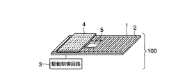
図1は、本発明の第1の実施形態に係るシャッタ装置100の概略図である。即ち、このシャッタ装置100は、それぞれ所定の間隔をおいて配置された複数の帯状の駆動電極2と当該シャッタ装置100に入射してきた光が通過する開口5とが設けられた固定基板1と、この固定基板1に対向するように配置されているエレクトレット加工が施された薄葉体の移動子4と、駆動電極2に交番電圧を印加する駆動制御回路3とから構成されている。ここで、エレクトレット加工とは、誘電体を永久的に電気分極状態とすることにより、固定電荷を保持させるようにする加工処理のことである。また、駆動電極2は、移動子4の移動方向(紙面左右方向)に直交するように配置する。
[First Embodiment]
FIG. 1 is a schematic diagram of a
図1のシャッタ装置100においては、駆動電極2に印加した電圧により移動子4が有する固定電荷に作用させる静電気力を変化させて、移動子4を移動させる。ここで、この図1においては、複数の駆動電極2を、開口5以外のほぼ全域にわたって設けるようにしている。このように、複数の駆動電極2を開口5以外のほぼ全域にわたって設ける、即ち、複数の駆動電極2を、その総面積が最大となるように設けることにより、移動子4の駆動力を大きくすることができる。
In the
ここで、図1において、開口5は四角形の形状をしているが、四角形に限らず、円形等でも良いことは言うまでもない。また、この第1の実施形態の固定基板1は、開口5が設けられている例について説明しているが、固定基板1以外の領域で光を通過させる場合や、固定基板1と駆動電極2とが共に光を透過する部材で構成されていれば、開口5を固定基板1に設ける必要はない。この場合には駆動電極2を移動子4のほぼ全域にわたって設けることができる。
Here, in FIG. 1, the
図2(a)及び図2(b)は、図1の構成を有するシャッタ装置100の開閉動作について説明するための図である。ここで、図2(a)は、開口5が露出した状態、即ちシャッタが開いた状態を示す。即ち、この状態では、シャッタ装置100に入射してきた光が開口5を通過する。一方、図2(b)は、開口5が移動子4によって遮光されている状態、即ちシャッタが閉じた状態を示す。
2A and 2B are diagrams for explaining the opening / closing operation of the
次に、図3(a)から図3(c)と図4を参照して移動子4について説明する。図3(a)は、図1の移動子4の一例を示す断面図である。即ち、図3(a)の移動子4は、エレクトレット加工が施された薄膜41(以下、薄膜41と称する)と遮光膜としての金属膜42とが積層されて構成されている。ここで、薄膜41には、例えばFEP(fluoro ethylene propylene)の薄膜を用いればよい。このFEP薄膜に対して例えばコロナ放電等を行って、薄膜をエレクトレット化する。
Next, the
このように薄膜41に金属膜42を積層することにより、移動子4における光の透過率を著しく下げることができる。また、移動子全体の厚さを数μm程度まで小さくすることが可能である。これにより、移動子4を軽量化できる。ここで、薄膜41の厚さを薄くするほど、エレクトレット加工する際の電荷の帯電効率が良くなる。これにより、移動子4の固定電荷密度を大きくすることができる。なお、金属膜42は、遮光性が高い膜であれば金属膜に限るものではない。
Thus, by laminating the
図3(b)は、移動子4の別の例の断面図である。即ち、図3(b)の移動子4は、エレクトレット化処理が施された薄膜41と、金属膜42と、光の透過率が約1〜5%である吸収部材としての薄膜43(以下、薄膜43と称する)とが積層されて構成されている。ここで、薄膜43は、例えば誘電体薄膜に黒塗料を塗布して構成すればよい。
FIG. 3B is a cross-sectional view of another example of the
このように、金属膜42と薄膜43とを薄膜41に積層することにより、光の透過率を下げることができると共に、金属膜42からの光の乱反射を防止することができる。これにより、遮光性が高く、かつ軽量の移動子4を作成できる。更に、薄膜43による光の乱反射を防止する作用により、このシャッタ装置をカメラ等に用いた場合の撮像品質を向上させることができる。
Thus, by laminating the
図3(c)は、移動子4の更に別の例の断面図である。即ち、図3(c)の移動子4は、エレクトレット化処理が施された薄膜41と、薄膜41よりも弾性率の大きな部材で構成された薄膜、例えばプラスチック薄膜あるいはガラス薄膜等の薄膜44(以下、薄膜44と称する)とが積層されて構成されている。このように弾性率の大きな薄膜44を薄膜41に積層することにより移動子4の剛性があがる。これにより、移動子4をより正確な平面に近づけることができ、この結果、移動子4とそれぞれの駆動電極2との距離を均一にすることができる。これにより、移動子4の駆動力を増加させることができる。
FIG. 3C is a cross-sectional view of still another example of the
図4は、薄膜41の別の例の断面図である。この図4の薄膜41は、被エレクトレット化薄膜45に局所的に複数のエレクトレット加工が施されている。この図4において、エレクトレット化された複数の部位46は、それぞれ所定の間隔で設けられているが、異なる間隔で設けるようにしても良い。
FIG. 4 is a cross-sectional view of another example of the
図4のように、エレクトレット化された複数の部位46の間隔を駆動電極2の間隔に対応させることにより、局所的にエレクトレット化していない場合に比べて移動子4に働く駆動力を増倍させることができる。
As shown in FIG. 4, the drive force acting on the moving
次に、図5を参照して固定基板1について説明する。図5は、固定基板1と駆動電極2の一例を示す断面図である。即ち、図5に示すように、固定基板1上には複数の駆動電極2が設けられている。そして、固定基板1における駆動電極2が設けられている側の面は、絶縁層11で覆われている。ここで、図5の例では、固定基板1の材質をガラス、駆動電極2の材質をアルミニウム、絶縁層11の材質をシリコン酸化膜としている。このように固定基板1を絶縁層11で覆うようにすることにより、隣接した駆動電極同士が絶縁されるので、静電気力が効率良く移動子4に働くようになる。
Next, the fixed
なお、固定基板1に設ける駆動電極2は、必ずしも図5に示すように等間隔で配置する必要はない。即ち、駆動電極2の配置は、移動子4のエレクトレット化された部位に対して充分な静電気力を作用させることができるのであれば、図5の配置に限定されない。
Note that the
次に、図6(a)から図6(d)を参照して、第1の実施形態に係るシャッタ装置の動作原理について説明する。ここで、移動子4は、図4のように所定の間隔で局所的にエレクトレット加工が施された移動子である。即ち、被エレクトレット化薄膜45にエレクトレット化された複数の部位46が所定の間隔で設けられている。ここで、エレクトレット化された複数の部位46は、駆動電極2に対する表面に負の電荷が存在するように帯電されている。また、駆動電極2は、駆動制御回路3に接続されている。これにより、駆動制御回路3によって駆動電極2に電圧が印加される。ここで、駆動制御回路3は、3相電源回路を想定して図示しているがこれに限るものではない。
Next, the principle of operation of the shutter device according to the first embodiment will be described with reference to FIGS. 6 (a) to 6 (d). Here, the
即ち、図6(a)に示すように、駆動制御回路3により、第1相(左端を第1相とする)に正、第2及び第3相に負の電圧を印加すると、第1相に接続されている駆動電極2と移動子4とがそれぞれ逆符号に帯電しているので、移動子4と駆動電極2との間に吸引力が働く。一方、第2及び第3相に接続されている駆動電極2と移動子4とはそれぞれ同符号に帯電しているので、移動子4と駆動電極2との間に反発力が発生する。この結果、移動子4が移動して図6(b)に示す状態になる。この図6(b)の状態で、第1及び第3相に負、第2相に正の電圧を印加すると、移動子4が移動して図6(c)に示す状態になる。更に図6(c)の状態で、第1及び第2相に負、第3相に正の電圧を印加すると、移動子4が移動して図6(d)の状態になる。以後同様にして第1相、第2相、第3相の順に正の電圧を印加していくと、移動子4は紙面に向かって右から左に移動することになる。また、逆に第3相、第2相、第1相の順に正の電圧を印加していくと、移動子4は紙面に向かって左から右に移動することになる。
That is, as shown in FIG. 6A, when the
即ち、遮光膜としての移動子4をこのようにして移動させることによって、シャッタの開閉動作が行われる。ここで、移動子4の表面には固定電荷が存在しているので、誘電電荷型アクチュエータ方式と比べて低電圧で大きな駆動力を得ることができる。
That is, the opening / closing operation of the shutter is performed by moving the
図7は、移動子4を駆動する際の電圧パターンの例を示した図である。この図7において、横軸は時間を示し、縦軸は駆動電極2への印加電圧の大きさを示す。ここで、図7の例では、駆動電極2に矩形波の電圧を印加している。
FIG. 7 is a diagram showing an example of a voltage pattern when driving the
即ち、図7のように第1の実施形態では、移動子4の駆動時における時刻0(移動子4の駆動開始時刻)から時刻t0までの範囲において、駆動電極2に印加する電圧の周波数を時間とともに大きくする。そして、時刻t0後は駆動電極2に印加する電圧の周波数を一定とする。
That is, in the first embodiment as shown in FIG. 7, the range of times during the driving of the moving
このように電圧を印加することにより、移動子4の初動時において十分に加速が働いていない場合に、次の駆動電極2によって吸引される距離まで到達せず、移動子4が脱調してしまうことを防ぐことができる。ここで、図7のようなパターンで電圧を印加しなくとも、駆動電極2のピッチ間隔や駆動電極2の幅を図8(a)から図8(c)に示すように設定することによって同様の効果を得ることができる。ここで、図8(a)は、移動子4が時刻0から時刻t0までに移動する領域(初動領域)における駆動電極のピッチ間隔P0を、その他の領域のピッチ間隔P1よりも狭く設定する例である。また、図8(b)は、上記初動領域における駆動電極のピッチ間隔P0を、その他の領域のピッチ間隔P1よりも狭く設定すると共に、駆動電極の幅W0を、その他の領域の幅W1よりも狭く設定する例である。さらに、図8(c)は、上記初動領域における駆動電極のピッチ間隔及び駆動電極の幅を、その他の領域に向かう方向(紙面右方向)に対して徐々に大きくなるように設定する例である。
By applying the voltage in this manner, when the acceleration is not sufficiently performed at the time of the initial movement of the moving
図9は、電源投入時において駆動制御回路3によって行われる制御について示したフローチャートである。即ち、電源投入時において、駆動制御回路3は、移動子4を所定位置に移動させるように電圧印加を行う(ステップS1)。続いて、駆動制御回路3は、移動子4が所定位置にあるか否かを判定し(ステップS2)、この所定位置にないと判定した場合に、ステップS1に戻り、再び移動子4を移動させる。一方、所定位置にあると判定した場合には、移動子4の移動指示がなされるまで待機する。
FIG. 9 is a flowchart showing the control performed by the
ここで、ステップS1の判定には、容量センサ回路により行う。この容量センサ回路は、例えば図10(a)に示すようにして駆動電極2に接続する。即ち、容量センサ回路6は、固定基板1の1端部(図では左端)に設置されている駆動電極21と駆動制御回路3とに接続されている。ここで、図10(a)は、電源非投入時の固定基板1と移動子4との位置関係を示している。図9で説明したように電源投入後、駆動制御回路3は、移動子4を容量センサ回路6に繋がれた駆動電極21が設置されている位置(図9の所定位置)に移動させるような制御を行う。
Here, the determination in step S1 is performed by a capacitance sensor circuit. This capacitance sensor circuit is connected to the
図10(b)は、移動子4が駆動電極21と重なる位置まで移動した状態を示す。移動子4が駆動電極21と重なる位置まで移動すると、駆動電極21と移動子4とによって形成されるコンデンサの電気容量が大きく変化する。この電気容量の変化が、容量センサ回路6によって検出される。これにより、駆動制御回路3は、移動子4が所定位置まで移動したことを判定し、移動子4を停止させる。
FIG. 10B shows a state where the
即ち、電源を入れていない状態では、移動子4の位置が不定であるが、電源投入時に常に所定位置に移動子4を移動させるように制御することによって、移動子4の制御性があがると共に、移動子4の駆動の効率が増加する。
That is, when the power is not turned on, the position of the
ここで、以上説明したシャッタ装置100の移動子4は、図11に示すように封止しておくようにすることがより好ましい。即ち、図11は、固定基板1と、保護部材51と、封止部材52とで移動子4を完全に封止した例である。ここで、保護部材51は、例えばガラス薄板であり、封止部材52はシリコンである。このように移動子4を封止しておけば、移動子4は温度、湿度、塵、及び埃等の影響を受けることがない。これにより、エレクトレット加工が施された薄葉体が持つ固定電荷量が、温度、湿度、塵、及び埃等の影響を受けて減衰してしまうのを防止することができる。ここで、図11の例では、駆動電極2も封止されているので、駆動電極2の性能劣化も防ぐことができる。
Here, it is more preferable that the
[第2の実施形態]
次に、本発明の第2の実施形態について説明する。この第2の実施形態は、第1の実施形態において説明したシャッタ装置の応用としての、低電圧かつ高速でシャッタ駆動を行うことが可能な薄型のフォーカルプレンシャッタ装置である。
[Second Embodiment]
Next, a second embodiment of the present invention will be described. This second embodiment is a thin focal plane shutter device capable of shutter driving at a low voltage and at a high speed as an application of the shutter device described in the first embodiment.
例えば、レンズシャッタ機構の場合、絞りの位置にシャッタ機構が設置されていなければならない。ここで、レンズのフォーカス駆動等の際には、絞りの位置が移動するので、シャッタ機構全体を移動させる機構が不可欠となる。このため、レンズシャッタ機構では、小型化が困難である。一方、フォーカルプレンシャッタ機構は、撮像素子の直前にシャッタ機構を設置するので、フォーカス移動等の際にもシャッタ機構を固定したままで良い。このため、シャッタ機構を移動させる機構が不必要であり、小型化が可能である。 For example, in the case of a lens shutter mechanism, the shutter mechanism must be installed at the stop position. Here, a mechanism for moving the entire shutter mechanism is indispensable because the position of the diaphragm moves when the lens is driven to focus. For this reason, it is difficult to reduce the size of the lens shutter mechanism. On the other hand, since the focal plane shutter mechanism is provided with a shutter mechanism immediately before the image sensor, the shutter mechanism may be fixed even during focus movement or the like. For this reason, a mechanism for moving the shutter mechanism is unnecessary, and the size can be reduced.
図12は、開口5を有した固定基板1と移動子4から構成されるシャッタ装置101と、このシャッタ装置101と同様の構成を有する固定基板19と移動子49とから構成されるシャッタ装置102とから構成されるフォーカルプレンシャッタの構成図である。この図12においては、例えば移動子49を先幕とし、移動子4を後幕として駆動させることによって、低電圧で高速駆動のフォーカルプレンシャッタを構成することができる。また、図12は、先幕及び後幕が共に開いた状態を図示している。ここで、移動子49及び移動子4の駆動電圧は、同位相とすることがより望ましい。このように駆動電圧を同位相とすることにより、露光ムラを防ぐことができる。
FIG. 12 shows a
ここで、この図12で示したフォーカルプレンシャッタも第1の実施形態において説明した各種変形例を適用することができる。また、フォーカルプレンシャッタを有するカメラの測光方式として、フォーカルプレンシャッタの先幕における反射光を利用して測光を行う、所謂ダイレクト測光方式が用いられることがあるが、第2の実施形態のフォーカルプレンシャッタをこのようなダイレクト測光方式が対応可能なように構成しても良い。この場合には、先幕49に反射率が標準反射率となるような所定のパターンを形成しておけば良い。
Here, the various modifications described in the first embodiment can also be applied to the focal plane shutter shown in FIG. Further, as a photometry method for a camera having a focal plane shutter, a so-called direct photometry method in which the photometry is performed using reflected light from the front curtain of the focal plane shutter may be used. The focal plane according to the second embodiment is sometimes used. The shutter may be configured to be compatible with such direct photometry. In this case, a predetermined pattern may be formed on the
以上実施形態に基づいて本発明を説明したが、本発明は上記した実施形態に限定されるものではなく、本発明の要旨の範囲内で種々の変形や応用が可能なことは勿論である。 Although the present invention has been described based on the above embodiments, the present invention is not limited to the above-described embodiments, and various modifications and applications are naturally possible within the scope of the gist of the present invention.
更に、上記した実施形態には種々の段階の発明が含まれており、開示される複数の構成要件の適当な組合せにより種々の発明が抽出され得る。例えば、実施形態に示される全構成要件からいくつかの構成要件が削除されても、発明が解決しようとする課題の欄で述べた課題が解決でき、発明の効果の欄で述べられている効果が得られる場合には、この構成要件が削除された構成も発明として抽出され得る。 Further, the above-described embodiments include various stages of the invention, and various inventions can be extracted by appropriately combining a plurality of disclosed constituent elements. For example, even if some constituent requirements are deleted from all the constituent requirements shown in the embodiment, the problem described in the column of the problem to be solved by the invention can be solved, and the effect described in the column of the effect of the invention Can be extracted as an invention.
1…固定基板、2…駆動電極、3…駆動制御回路、4…移動子、5…開口、6…容量センサ回路、51…保護部材、52…封止部材、100,101,102…シャッタ装置
DESCRIPTION OF
Claims (15)
上記固定基板に対向して配置され、少なくとも、永久的に電気分極状態とすることにより固定電荷を保持させるようにする加工処理であるエレクトレット加工が施された薄葉体で構成され、上記開口への光を遮光するための遮光膜を有する移動子と、
上記固定基板に設けられた駆動電極に印加する電圧を変化させることにより、上記エレクトレット加工によって上記移動子に生じる固定電荷に作用させる静電気力を変化させ、この静電気力により上記移動子を移動させて上記開口を遮光するように制御する駆動制御手段と、
を具備し、
上記固定基板は、上記移動子の移動開始位置から所定位置までの初動領域と、上記初動領域以外の駆動領域との2つの領域を有し、上記固定基板上の上記初動領域と上記駆動領域とにおいて、上記複数の駆動電極のピッチ間隔と上記複数の駆動電極の幅の少なくとも何れかが異なることを特徴とするシャッタ装置。 A fixed substrate having an opening provided with a plurality of drive electrodes arranged at predetermined intervals; and
The thin substrate is disposed opposite to the fixed substrate and is subjected to electret processing, which is a processing process for holding a fixed charge by at least permanently setting the electric polarization state . A moving element having a light-shielding film for shielding light ;
By changing the voltage applied to the drive electrode provided on the fixed substrate, the electrostatic force applied to the fixed charge generated on the moving element by the electret processing is changed, and the moving element is moved by the electrostatic force. Drive control means for controlling the opening to block light ;
Comprising
The fixed board has two areas, an initial movement area from a movement start position of the moving element to a predetermined position, and a drive area other than the initial movement area, and the initial movement area and the drive area on the fixed board The shutter device is characterized in that at least one of a pitch interval between the plurality of drive electrodes and a width of the plurality of drive electrodes is different .
Priority Applications (3)
| Application Number | Priority Date | Filing Date | Title |
|---|---|---|---|
| JP2003355460A JP4343644B2 (en) | 2003-10-15 | 2003-10-15 | Shutter device |
| US10/965,149 US7182530B2 (en) | 2003-10-15 | 2004-10-14 | Electrode shutter device with start area |
| US11/702,336 US7367722B2 (en) | 2003-10-15 | 2007-02-05 | Front and rear curtain shutter device with start area |
Applications Claiming Priority (1)
| Application Number | Priority Date | Filing Date | Title |
|---|---|---|---|
| JP2003355460A JP4343644B2 (en) | 2003-10-15 | 2003-10-15 | Shutter device |
Publications (3)
| Publication Number | Publication Date |
|---|---|
| JP2005121821A JP2005121821A (en) | 2005-05-12 |
| JP2005121821A5 JP2005121821A5 (en) | 2006-11-24 |
| JP4343644B2 true JP4343644B2 (en) | 2009-10-14 |
Family
ID=34509765
Family Applications (1)
| Application Number | Title | Priority Date | Filing Date |
|---|---|---|---|
| JP2003355460A Expired - Fee Related JP4343644B2 (en) | 2003-10-15 | 2003-10-15 | Shutter device |
Country Status (2)
| Country | Link |
|---|---|
| US (2) | US7182530B2 (en) |
| JP (1) | JP4343644B2 (en) |
Families Citing this family (6)
| Publication number | Priority date | Publication date | Assignee | Title |
|---|---|---|---|---|
| JP5033561B2 (en) * | 2007-09-26 | 2012-09-26 | 三洋電機株式会社 | Electrostatic generator |
| DE202013008329U1 (en) * | 2013-09-19 | 2015-01-05 | Schölly Fiberoptic GmbH | endoscope |
| DE102017115248B4 (en) * | 2017-07-07 | 2020-03-12 | Saf-Holland Gmbh | System for fixing a pivot bolt to a vehicle frame, vehicle frame for connecting a pivot bolt and method for mounting a pivot bolt on a vehicle frame |
| JP2020161652A (en) * | 2019-03-27 | 2020-10-01 | 三井化学株式会社 | Electret element, electret structure, sensor and electronic apparatus |
| CN113067977B (en) * | 2019-12-31 | 2023-04-18 | 中芯集成电路(宁波)有限公司 | Translation mechanism, forming method thereof, translation method and electronic equipment |
| CN111443825B (en) * | 2020-03-25 | 2022-09-23 | 维沃移动通信有限公司 | Electronic equipment and control method and control module thereof |
Family Cites Families (6)
| Publication number | Priority date | Publication date | Assignee | Title |
|---|---|---|---|---|
| JPS55144216A (en) * | 1979-04-27 | 1980-11-11 | Canon Inc | Electromagnetically driven slit exposure shutter |
| JP2721638B2 (en) * | 1993-11-25 | 1998-03-04 | 富士通株式会社 | Electrostatic actuator |
| JPH08220592A (en) | 1995-02-17 | 1996-08-30 | Minolta Co Ltd | Shutter mechanism of camera |
| JP3736915B2 (en) * | 1996-09-25 | 2006-01-18 | セイコープレシジョン株式会社 | Camera shutter control device |
| JP3215815B2 (en) * | 1998-09-02 | 2001-10-09 | 日本電産コパル株式会社 | Light shielding blades for optical equipment |
| JP2002112560A (en) * | 2000-09-28 | 2002-04-12 | Toshiba Corp | Electrostatic actuator and camera module employing the actuator |
-
2003
- 2003-10-15 JP JP2003355460A patent/JP4343644B2/en not_active Expired - Fee Related
-
2004
- 2004-10-14 US US10/965,149 patent/US7182530B2/en not_active Expired - Fee Related
-
2007
- 2007-02-05 US US11/702,336 patent/US7367722B2/en not_active Expired - Fee Related
Also Published As
| Publication number | Publication date |
|---|---|
| US7182530B2 (en) | 2007-02-27 |
| US20070133982A1 (en) | 2007-06-14 |
| US7367722B2 (en) | 2008-05-06 |
| US20050084261A1 (en) | 2005-04-21 |
| JP2005121821A (en) | 2005-05-12 |
Similar Documents
| Publication | Publication Date | Title |
|---|---|---|
| US8061910B2 (en) | Micro shutter having iris function, method for manufacturing the same, and micro camera module having the same | |
| JP3791847B1 (en) | Camera module and information terminal equipped with the camera module | |
| JP3966704B2 (en) | Electrostatic actuator, driving method of electrostatic actuator, and camera module using the same | |
| JP4343644B2 (en) | Shutter device | |
| US7462975B2 (en) | Actuator | |
| CN111343372A (en) | Camera module and electronic equipment | |
| US20060209427A1 (en) | Electrostatic actuator and image pickup apparatus using the same | |
| US20070139599A1 (en) | Comb-type electrode structure capable of large linear-displacement motion | |
| CN102636873B (en) | Foreign matter removal unit and optical apparatus having the same | |
| JP3793568B1 (en) | Camera module and information terminal equipped with the camera module | |
| JP2004061840A (en) | Electrophoretic light adjusting device, its driving method and apparatus using same | |
| CN113949759B (en) | Electronic equipment | |
| CN113132578B (en) | Displacement mechanism, driving method thereof and electronic device | |
| CN217087972U (en) | Device for acquiring super-resolution image | |
| JP2006033977A (en) | Electrostatic drive unit and driven body for use in the device | |
| JP2006038945A (en) | Light shielding curtain and electrostatic shutter apparatus | |
| JP2005331829A (en) | Electrostatic shutter device, optical equipment, and optical equipment having the shutter device, and camera | |
| JP4391076B2 (en) | Microactuator with holding mechanism and method for manufacturing the same | |
| JP2006018105A (en) | Light quantity controller and camera equipped with the same | |
| JP2006042415A (en) | Electrostatic drive unit, shutter, and image pick-up module | |
| JP3800820B2 (en) | Active micro optical element and image display device | |
| JP2006038885A (en) | Light quantity adjusting device and camera using the same | |
| JP3791846B1 (en) | Camera module and information terminal equipped with the camera module | |
| KR20150140682A (en) | Arcuate motion control in electrostatic actuators | |
| JP2005316327A (en) | Light quantity adjusting device and camera using the same |
Legal Events
| Date | Code | Title | Description |
|---|---|---|---|
| A521 | Written amendment |
Free format text: JAPANESE INTERMEDIATE CODE: A523 Effective date: 20061004 |
|
| A621 | Written request for application examination |
Free format text: JAPANESE INTERMEDIATE CODE: A621 Effective date: 20061004 |
|
| A977 | Report on retrieval |
Free format text: JAPANESE INTERMEDIATE CODE: A971007 Effective date: 20090113 |
|
| A131 | Notification of reasons for refusal |
Free format text: JAPANESE INTERMEDIATE CODE: A131 Effective date: 20090120 |
|
| A521 | Written amendment |
Free format text: JAPANESE INTERMEDIATE CODE: A523 Effective date: 20090306 |
|
| A131 | Notification of reasons for refusal |
Free format text: JAPANESE INTERMEDIATE CODE: A131 Effective date: 20090421 |
|
| A521 | Written amendment |
Free format text: JAPANESE INTERMEDIATE CODE: A523 Effective date: 20090515 |
|
| TRDD | Decision of grant or rejection written | ||
| A01 | Written decision to grant a patent or to grant a registration (utility model) |
Free format text: JAPANESE INTERMEDIATE CODE: A01 Effective date: 20090616 |
|
| A01 | Written decision to grant a patent or to grant a registration (utility model) |
Free format text: JAPANESE INTERMEDIATE CODE: A01 |
|
| A61 | First payment of annual fees (during grant procedure) |
Free format text: JAPANESE INTERMEDIATE CODE: A61 Effective date: 20090709 |
|
| FPAY | Renewal fee payment (event date is renewal date of database) |
Free format text: PAYMENT UNTIL: 20120717 Year of fee payment: 3 |
|
| FPAY | Renewal fee payment (event date is renewal date of database) |
Free format text: PAYMENT UNTIL: 20120717 Year of fee payment: 3 |
|
| FPAY | Renewal fee payment (event date is renewal date of database) |
Free format text: PAYMENT UNTIL: 20130717 Year of fee payment: 4 |
|
| LAPS | Cancellation because of no payment of annual fees |