JP4337467B2 - Inspection method for optical scanning device - Google Patents
Inspection method for optical scanning device Download PDFInfo
- Publication number
- JP4337467B2 JP4337467B2 JP2003293049A JP2003293049A JP4337467B2 JP 4337467 B2 JP4337467 B2 JP 4337467B2 JP 2003293049 A JP2003293049 A JP 2003293049A JP 2003293049 A JP2003293049 A JP 2003293049A JP 4337467 B2 JP4337467 B2 JP 4337467B2
- Authority
- JP
- Japan
- Prior art keywords
- substrate
- detection element
- synchronization detection
- light
- optical scanning
- Prior art date
- Legal status (The legal status is an assumption and is not a legal conclusion. Google has not performed a legal analysis and makes no representation as to the accuracy of the status listed.)
- Expired - Fee Related
Links
Images


Classifications
-
- H—ELECTRICITY
- H04—ELECTRIC COMMUNICATION TECHNIQUE
- H04N—PICTORIAL COMMUNICATION, e.g. TELEVISION
- H04N1/00—Scanning, transmission or reproduction of documents or the like, e.g. facsimile transmission; Details thereof
- H04N1/04—Scanning arrangements, i.e. arrangements for the displacement of active reading or reproducing elements relative to the original or reproducing medium, or vice versa
- H04N1/047—Detection, control or error compensation of scanning velocity or position
-
- G—PHYSICS
- G02—OPTICS
- G02B—OPTICAL ELEMENTS, SYSTEMS OR APPARATUS
- G02B26/00—Optical devices or arrangements for the control of light using movable or deformable optical elements
- G02B26/08—Optical devices or arrangements for the control of light using movable or deformable optical elements for controlling the direction of light
- G02B26/10—Scanning systems
- G02B26/12—Scanning systems using multifaceted mirrors
-
- G—PHYSICS
- G03—PHOTOGRAPHY; CINEMATOGRAPHY; ANALOGOUS TECHNIQUES USING WAVES OTHER THAN OPTICAL WAVES; ELECTROGRAPHY; HOLOGRAPHY
- G03G—ELECTROGRAPHY; ELECTROPHOTOGRAPHY; MAGNETOGRAPHY
- G03G15/00—Apparatus for electrographic processes using a charge pattern
- G03G15/04—Apparatus for electrographic processes using a charge pattern for exposing, i.e. imagewise exposure by optically projecting the original image on a photoconductive recording material
- G03G15/043—Apparatus for electrographic processes using a charge pattern for exposing, i.e. imagewise exposure by optically projecting the original image on a photoconductive recording material with means for controlling illumination or exposure
- G03G15/0435—Apparatus for electrographic processes using a charge pattern for exposing, i.e. imagewise exposure by optically projecting the original image on a photoconductive recording material with means for controlling illumination or exposure by introducing an optical element in the optical path, e.g. a filter
-
- H—ELECTRICITY
- H04—ELECTRIC COMMUNICATION TECHNIQUE
- H04N—PICTORIAL COMMUNICATION, e.g. TELEVISION
- H04N1/00—Scanning, transmission or reproduction of documents or the like, e.g. facsimile transmission; Details thereof
- H04N1/00519—Constructional details not otherwise provided for, e.g. housings, covers
- H04N1/00525—Providing a more compact apparatus, e.g. sheet discharge tray in cover
-
- H—ELECTRICITY
- H04—ELECTRIC COMMUNICATION TECHNIQUE
- H04N—PICTORIAL COMMUNICATION, e.g. TELEVISION
- H04N1/00—Scanning, transmission or reproduction of documents or the like, e.g. facsimile transmission; Details thereof
- H04N1/04—Scanning arrangements, i.e. arrangements for the displacement of active reading or reproducing elements relative to the original or reproducing medium, or vice versa
- H04N1/113—Scanning arrangements, i.e. arrangements for the displacement of active reading or reproducing elements relative to the original or reproducing medium, or vice versa using oscillating or rotating mirrors
- H04N1/1135—Scanning arrangements, i.e. arrangements for the displacement of active reading or reproducing elements relative to the original or reproducing medium, or vice versa using oscillating or rotating mirrors for the main-scan only
-
- H—ELECTRICITY
- H04—ELECTRIC COMMUNICATION TECHNIQUE
- H04N—PICTORIAL COMMUNICATION, e.g. TELEVISION
- H04N2201/00—Indexing scheme relating to scanning, transmission or reproduction of documents or the like, and to details thereof
- H04N2201/0077—Types of the still picture apparatus
- H04N2201/0082—Image hardcopy reproducer
-
- H—ELECTRICITY
- H04—ELECTRIC COMMUNICATION TECHNIQUE
- H04N—PICTORIAL COMMUNICATION, e.g. TELEVISION
- H04N2201/00—Indexing scheme relating to scanning, transmission or reproduction of documents or the like, and to details thereof
- H04N2201/04—Scanning arrangements
- H04N2201/047—Detection, control or error compensation of scanning velocity or position
- H04N2201/04701—Detection of scanning velocity or position
- H04N2201/0471—Detection of scanning velocity or position using dedicated detectors
- H04N2201/04713—Details of the detector arrangement, e.g. non-standard position, optical details
-
- H—ELECTRICITY
- H04—ELECTRIC COMMUNICATION TECHNIQUE
- H04N—PICTORIAL COMMUNICATION, e.g. TELEVISION
- H04N2201/00—Indexing scheme relating to scanning, transmission or reproduction of documents or the like, and to details thereof
- H04N2201/04—Scanning arrangements
- H04N2201/047—Detection, control or error compensation of scanning velocity or position
- H04N2201/04701—Detection of scanning velocity or position
- H04N2201/04729—Detection of scanning velocity or position in the main-scan direction
-
- H—ELECTRICITY
- H04—ELECTRIC COMMUNICATION TECHNIQUE
- H04N—PICTORIAL COMMUNICATION, e.g. TELEVISION
- H04N2201/00—Indexing scheme relating to scanning, transmission or reproduction of documents or the like, and to details thereof
- H04N2201/04—Scanning arrangements
- H04N2201/047—Detection, control or error compensation of scanning velocity or position
- H04N2201/04701—Detection of scanning velocity or position
- H04N2201/04744—Detection of scanning velocity or position by detecting the scanned beam or a reference beam
Description
本発明は、レーザプリンタなどに用いられる光走査装置の検査方法に関する。 The present invention relates to an inspection method for an optical scanning device used in a laser printer or the like.
従来より、レーザ素子から射出されるレーザ光を記録情報に基づき変調し、そのレーザ光を、ポリゴンミラーのような反射体を備えた光走査装置を用いて偏向走査して感光体面上に結像させることにより、感光体上に静電潜像を形成し、この静電潜像を現像剤により可視像化することで記録するレーザプリンタなどの画像形成装置が知られている。 Conventionally, laser light emitted from a laser element is modulated based on recorded information, and the laser light is deflected and scanned using an optical scanning device having a reflector such as a polygon mirror to form an image on the surface of the photoreceptor. An image forming apparatus such as a laser printer is known in which an electrostatic latent image is formed on a photosensitive member, and the electrostatic latent image is recorded by making the electrostatic latent image visible with a developer.
このような画像形成装置に用いられる光走査装置では、一般に走査する偏向光の一部を取り込んで像形成のための同期検出を行う同期検出素子が設けられており、この同期検出素子により、繰り返し行われる走査と感光体に像形成を行うための記録情報との同期が取られている。 In an optical scanning device used in such an image forming apparatus, a synchronization detecting element is generally provided that performs synchronization detection for image formation by capturing a part of the deflected light to be scanned. The scanning to be performed is synchronized with the recording information for forming an image on the photosensitive member.
また、同期検出素子に導かれる偏向光は、同期検出素子の受光感度や同期検出の精度を確保するために、同期検出素子に入射する近傍で偏向光の光束を充分絞っておく必要がある。そのため、ポリゴンミラーの偏向点から同期検出素子までの光路の長さをポリゴンミラーの偏向点から画像形成装置本体の感光体までの光路の長さとほぼ等しくしておくことが望ましかった。 Further, the deflected light guided to the synchronization detection element needs to be sufficiently narrowed in the vicinity of the incident light to the synchronization detection element in order to ensure the light receiving sensitivity of the synchronization detection element and the accuracy of synchronization detection. For this reason, it has been desirable to make the length of the optical path from the deflection point of the polygon mirror to the synchronization detecting element approximately equal to the length of the optical path from the deflection point of the polygon mirror to the photosensitive member of the image forming apparatus main body.
ところが、半導体レーザ素子と同期検出素子とを基板の同一面上に実装する従来の光走査装置では、ポリゴンミラーの偏向点から同期検出素子までの光路の長さをポリゴンミラーの偏向点から感光体までの光路の長さとほぼ等しくすることが望ましいという観点から、半導体レーザ素子、同期検出素子および回路素子、コンデンサなど関連部品の基板上での配置に関する制約が生じ、配置の自由度が少なくなるという問題があった。 However, in the conventional optical scanning device in which the semiconductor laser element and the synchronization detection element are mounted on the same surface of the substrate, the length of the optical path from the deflection point of the polygon mirror to the synchronization detection element is determined from the deflection point of the polygon mirror to the photosensitive member. From the standpoint that it is desirable to make the length of the optical path approximately equal to the length of the optical path, there are restrictions on the placement of related parts such as semiconductor laser elements, synchronous detection elements and circuit elements, capacitors on the substrate, and the degree of freedom of placement is reduced. There was a problem.
この問題に対処するために、下記特許文献などでは基板の半導体レーザ素子を取り付ける面とは異なる面に同期検出素子を取り付けることにより、ポリゴンミラーの偏向点から同期検出素子までの光路の長さとポリゴンミラーの偏向点から感光体までの光路の長さとをほぼ等しくする技術が開示されている。
しかしながら、上記の技術では半導体レーザ素子や同期検出素子等を取付ける基板が上下方向に置かれたいわゆる基板縦置き型の光走査装置であるため、基板に半導体レーザ素子や同期検出素子および回路素子、コンデンサなどの関連部品を実装すると、基板の上下方向の寸法が増大し、そのため光走査装置の上下方向の寸法が増大するという問題があった。 However, in the above technique, since the substrate for mounting the semiconductor laser element, the synchronous detection element, etc. is a so-called vertical substrate type optical scanning device, the semiconductor laser element, the synchronous detection element, the circuit element, When a related component such as a capacitor is mounted, the vertical dimension of the substrate increases, and thus the vertical dimension of the optical scanning device increases.
一方、半導体レーザ素子や同期検出素子等を取り付ける基板を、光走査装置の筐体に対して平行に置かれたいわゆる基板横置き型の場合、同期検出素子における光路を確保しアライメントのチェックを可能としつつ回路素子や関連部品を実装するのは困難であった。 On the other hand, if the substrate to which the semiconductor laser element, synchronization detection element, etc. are mounted is a so-called horizontal mounting type that is placed parallel to the optical scanning device housing, the optical path of the synchronization detection element is secured and alignment can be checked However, it was difficult to mount circuit elements and related parts.
本発明は、このような事情に鑑みなされたもので、その目的は、基板横置き型の場合において、基板に回路素子や関連部品を実装しつつ同期検出素子における光路を確保しアライメントのチェックを可能とする光走査装置の検査方法を提供することを目的とする。 The present invention has been made in view of such circumstances, and its purpose is to check the alignment by securing the optical path in the synchronous detection element while mounting the circuit element and related parts on the board in the case of the horizontal board type. It is an object of the present invention to provide an optical scanning device inspection method that enables this.
上記課題を達成するため、請求項1に記載の発明の光走査装置の検査方法は、回路素子が組み付けられた基板と、該基板の上面に組み付けられた回路素子により出力が制御される光源と、該光源から射出される光束を偏向走査する反射体と、該反射体からの偏向光の一部を取り込み、像形成のための同期検出を行う同期検出素子と、該同期検出素子へ前記反射体からの偏向光を導入するための集光レンズと、前記基板、光源、反射体及び同期検出素子が組み付けられる筐体とを備えた光走査装置の検査方法であって、前記基板は、前記筐体の上面又は下面と平行に組みつけられるとともに、貫通孔を有し、前記同期検出素子は、前記基板の下面に組み付けられ、前記基板の下側に設けられた光路を通る前記偏向光を検知し、前記偏向光を通過させるための検査孔が形成された検査板を前記貫通孔に挿通することで、前記同期検出素子と前記集光レンズの組み付けアライメントを検査することを特徴としている。 In order to achieve the above object, an inspection method for an optical scanning device according to a first aspect of the present invention includes a substrate on which a circuit element is assembled, and a light source whose output is controlled by the circuit element assembled on the upper surface of the substrate. a reflector for deflecting and scanning the light beam emitted from the light source, captures some of the deflected light from the reflector, the reflector and the synchronization detection element for synchronization detection for image formation, the synchronous detecting element An inspection method for an optical scanning device comprising a condensing lens for introducing deflected light from a body, and a housing in which the substrate, the light source, a reflector, and a synchronization detection element are assembled. the housing of the upper or lower surface parallel to the assembled Rutotomoni has a through hole, the synchronization detection element is assembled on the lower surface of the substrate, said polarized light passing through the optical path provided on the lower side of the substrate It detects, passing the deflected light The inspection test plate having holes formed therein for by inserted into the through hole, it is characterized in that you examine the assembling alignment of the condenser lens and the synchronization detection element.
また、請求項2に記載の発明は、請求項1記載の発明において、前記光源は、少なくとも一つの発光素子を備えた半導体レーザであることを特徴としている。 Further, the invention according to claim 2, in the invention of claim 1, wherein said light source is characterized in that a semiconductor laser with at least one light emitting device.
また、請求項3に記載の発明は、請求項1または2記載の発明において、前記検査孔の面積は、前記貫通孔に挿通された前記検査板と前記同期検出素子との間に配設された前記集光レンズの有効面積よりも小さいことを特徴としている。
Also, the invention according to
このような構成によると、前記検査孔を通過しないが前記集光レンズの有効面積を通過する前記偏向光はマージンとなる。従って、そのマージン内で前記同期検出素子と前記集光レンズとの組み付けアライメントが変動しても前記偏向光は前記同期検出素子によって検知されることができる。 According to such a configuration, the deflected light that does not pass through the inspection hole but passes through the effective area of the condenser lens becomes a margin. Therefore, even if the assembly alignment between the synchronization detection element and the condenser lens varies within the margin, the deflected light can be detected by the synchronization detection element.
また、請求項4に記載の発明は、請求項1ないし3のいずれかに記載の発明において、前記基板を下側から支持する前記筐体に、前記筐体の強度および剛性を増加させるリブが形成されていることを特徴としている。 According to a fourth aspect of the present invention, in the invention according to any one of the first to third aspects, a rib that increases the strength and rigidity of the casing is provided on the casing that supports the substrate from below. It is characterized by being formed.
このような構成によると、リブを設けることにより前記筐体の強度および剛性を増加させることができる。それにより、前記筐体の歪や変形が防止され、前記偏向光の光路変化の発生を防止することができる。さらに、前記基板の下面に実装部品が組み付けられていないのでリブの形状、大きさおよび配置を自由に選択することができる。 According to such a configuration, it is possible to increase the strength and rigidity of the housing by providing the re-drive. As a result, distortion and deformation of the casing can be prevented, and an optical path change of the deflected light can be prevented. Furthermore, since no mounting component is assembled to the lower surface of the substrate, the shape, size and arrangement of the ribs can be freely selected.
以下に、本発明の一実施形態を、添付図面に基づいて説明する。
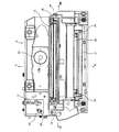
図1は、本発明に係る光走査装置の一実施形態としてのスキャナの正面部を示す。図2は、スキャナの上面カバーを示す図である。図3は、スキャナの裏面図である。図4は、スキャナの基板が取り外された状態を示す透視図である。
Hereinafter, an embodiment of the present invention will be described with reference to the accompanying drawings.
FIG. 1 shows a front portion of a scanner as an embodiment of an optical scanning device according to the present invention. FIG. 2 is a diagram illustrating a top cover of the scanner. FIG. 3 is a rear view of the scanner. FIG. 4 is a perspective view showing a state where the substrate of the scanner is removed.
図1から図4までを用いて、スキャナの構成について説明する。
図1において、スキャナ60の正面部は、光源3、基板4、ポリゴンモータ12、Fシータレンズ14、折り返しミラー16および筐体22などで構成されている。
The configuration of the scanner will be described with reference to FIGS.
In FIG. 1, the front portion of the
光源3は、スキャナ60の左端部(図1のLH方向側)に配置され、ネジ6によってレーザダイオードホルダ1に取り付けられている。レーザダイオードホルダ1は、ネジ2によって筐体22に固定されている。なお、本明細書では以後、図1のLH方向をスキャナ60の左側、図1のRH方向をスキャナ60の右側、図1のF方向をスキャナ60の前側、図1のR方向をスキャナ60の後側、図1の紙面の手前側をスキャナ60の上側および図1の紙面の向こう側をスキャナ60の下側として説明する。
The
光源3は、2個の図示しない発光素子を備えた半導体レーザである。
基板4は、スキャナ60の前側の左端部に配設された平板であり、その上面にはコネクタ31、回路素子32a〜32e、コンデンサ33aなどが実装され、その下面は半田で接続された電気回路面で構成されている。基板4の下面には、後述の同期検出素子48が取り付けられている。同期検出素子48が、基板4の下面に取り付けられているので基板4の上面に実装されるコネクタ31、回路素子32a〜32e、コンデンサ33aなどの配置を自由に選択することができる。基板4は、ネジ5によって筐体22に固定されている。
The
The substrate 4 is a flat plate disposed at the left end portion on the front side of the
基板4の上面に実装された回路素子32a〜32eは、光源3の2個の図示しない発光素子の出力を制御するためのものであり、例えば、半導体レーザの出力を調整するための発光ボリューム、半導体レーザの出力を変調するための変調ボリュームおよび半導体レーザの出力を粗調整あるいは微調整するための出力調整ボリュームである。このように2個の発光素子を用いることにより、レーザプリンタの解像度を高めることができる。
ポリゴンモータ12は、スキャナ60の前側のほぼ中央部に配設されており、その回転軸12bの周りに回転する反射体12aが一体的に成形されている。ポリゴンモータ12は、ネジ13によって筐体22に取り付けられている。光源3とポリゴンモータ12との間には、光源3の側から順にコリメータレンズ8、コリメータスリット9およびシリンドリカルレンズ11が配置されている。コリメータレンズ8は、コリメータレンズホルダ7によって支持されている。
The
Fシータレンズ14は、スキャナ60のほぼ中心部に押さえバネ36によって固定されている。
なお、スキャナ60の上面は、図2に示す上面カバー25によって覆われ、スキャナ60の正面側に配置された部品が保護されている。上面カバー25は、上面カバー取付けネジ26によってスポンジ30a、30b、30cなどを介して筐体22に取り付けられている。
The F-
Note that the upper surface of the
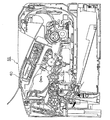
図3に示すスキャナ60の裏面において、基板4の下面にはビームディテクトスリット19およびビームディテクトミラー20が取り付けられている。図4のスキャナ60の基板4が取り外された状態を示す透視図において、ビームディテクトミラー20の右側(図4のRH方向側)には、集光レンズ21と同期検出素子48が配設されている。
On the back surface of the
また、図4に示すように、基板4の下側には筐体22にリブ49が基板4と交差する方向に設けられている。基板4の下面には、前述のコネクタ31、回路素子32a〜32e、コンデンサ33aなどが実装されていないので、リブ49の形状、大きさおよび配置を自由に選択することができる。リブ49は、筐体22の強度および剛性を増加させることができるので、それにより、筐体22の熱による歪や変形が防止され、スキャナ60内における光束や偏向光の光路変化の発生が防止される。
Further, as shown in FIG. 4, a
集光レンズ21と同期検出素子48をこのように配設すると、光源3から同期検出素子48までの光路を規定する光学素子が配置された光学経路において、同期検出素子48の受光感度や同期検出の精度を確保するとともに、スキャナ60の上下方向および前後左右方向の寸法もコンパクトにすることができる。
When the
スキャナ60の裏面は、図5に示すような裏面カバー27で覆われている。裏面カバー27は、裏面カバー取付けネジ28によって筐体22に取り付けられ、スキャナ60の裏面に配設された部品を保護している。
The back surface of the
次に、図1、図3および図4を参照して集光レンズ21と同期検出素子48の組み付けアライメントの検査方法について説明する。
図1に示す光源3から射出された光束は、コリメータレンズホルダ7によって支持されたコリメータレンズ8を通過する。コリメータレンズ8を通過して平行光となった光束は、コリメータスリット9を通過した後、さらにシリンドリカルレンズ11を通過する。シリンドリカルレンズ11を通過した光束は、ポリゴンモータ12に一体的に形成され高速で回転する反射体12aで偏向走査されて偏向光を生ずる。この偏向光は、Fシータレンズを通過し、スキャナ60の後側(図1のR方向側)に配設され押さえバネ34によって取り付けられている折り返しミラー16によって直角に光路が変更され、その偏向光の一部はスキャナ60の裏面に到達する。
Next, an assembly alignment inspection method for the
A light beam emitted from the
スキャナ60の裏面に到達した偏向光は、図3において折り返しミラー17によって直角に光路が偏向され、シリンドリカルレンズ15を通過した後ビームディテクトミラー20に向かう。ビームディテクトミラー20で折り返された偏向光はビームディテクトスリット19を通過し、集光レンズ21に到達する。集光レンズ21を通過した偏向光は、同期検出素子48によって検知され、同期検出素子48から検知信号がレーザプリンタの図示しない制御部に送信される。
The deflected light reaching the back surface of the
ここで、基板4が筐体22に組み付けられてしまうと、基板4の下面に取付けられた集光レンズ21と同期検出素子48の組み付けアライメントを検査することができない。そのため、図7に示すように、集光レンズ21の左側(図7のLH方向)の基板4に貫通孔4aが設けられている。この貫通孔4aに検査板59を上方から挿通し集光レンズ21と同期検出素子48の組み付けアライメントを検査することができる。
Here, if the board | substrate 4 is assembled | attached to the housing | casing 22, the assembly | attachment alignment of the condensing
検査板59は、図8に示すような平板でその一端部に例えば円形の検査孔59aが形成されている。検査孔59aの面積を集光レンズ21の有効面積よりも小さくすることにより、検査孔59aを通過しないが集光レンズ21の有効面積を通過する偏向光はマージンとなる。従って、そのマージン内で同期検出素子48と集光レンズ21との組み付けアライメントが変動しても、偏向光は同期検出素子48によって検知されることができる。
The
次に、レーザプリンタに設けられたスキャナ60のポリゴンモータ12の冷却手段について、図3および図6を参照して説明する。
図3に戻り、スキャナ60のポリゴンモータ12の冷却手段は裏面側の前側(図3のF方向側)の右端部に設けられている。図3のC方向から見た冷却手段を図6に概略的に示す。
Next, cooling means for the
Returning to FIG. 3, the cooling means of the
図6において、冷却手段はファン52とダクト55とから構成されている。すなわち、ダクト55の右端部(図6のRH方向側)にはファン52が配置されている。ダクト55は、ファン52とその左方(図6のLH方向側)にあるポリゴンモータ12との間を連通している。ポリゴンモータ12を回転させる回転軸12bは、モータスペーサ43に支持されておりモータスペーサ43は筐体22に取り付けられている。モータスペーサ43は、円板であり例えばアルミニウム材から作られている。
In FIG. 6, the cooling means includes a
ファン52は、電動ファンでありファンホルダ53に支持されている。ファンホルダ53は、図6に示すように、例えば発泡ウレタン材などから形成されたスポンジ54を介して筐体22の外壁部22aと画像形成装置本体に取付けられたプレート51に保持されている。従って、ファン52の回転により生じる振動がスキャナ60の筐体22とプレート51とに伝達されることがないので、偏向光の光路変化が生じなく、集光レンズ21と同期検出素子48の組み付けアライメントに影響を及ぼす懸念がない。
The
ダクト55は、筐体22の外壁部22aとスキャナ60を囲むプレート51とで構成されている。このように構成すると、ダクト55のための専用部品を設けなくてもよいので、部品点数を少なくすることができる。
The
また、図6に示すように、ダクト55の形状をファン52の近傍における断面積よりもポリゴンモータ12の近傍における断面積のほうが小さくなるように形成すると、ポリゴンモータ12の近傍におけるダクト55aを通過する空気の流速がファン52の近傍におけるダクト55bを通過する空気の流速よりも増加し、ポリゴンモータ12の冷却効率を高めることができる。
Further, as shown in FIG. 6, when the shape of the
さらに、モ−タスペーサ43がアルミニウム材で作られているのでアルミニウムの大きい熱伝導率のためにモータスペーサ43が速やかに冷却される。それにより、ポリゴンモータ12の冷却効率をさらに一層高めることができる。
Furthermore, since the
図9は、本発明に係るスキャナ60が好適に用いられたレーザプリンタ65の要部側断面図である。図9において、符号66は感光体を示す。
以上、本発明に係る一実施形態について説明したが、本発明の実施の形態は、上記実施例に何ら限定されることなく、本発明の技術的範囲に属する限り種々の形態を取りうることはいうまでもない。
FIG. 9 is a sectional side view of a main part of a
Although one embodiment according to the present invention has been described above, the embodiment of the present invention is not limited to the above-described embodiment, and can take various forms within the technical scope of the present invention. Needless to say.
1・・・レーザダイオードホルダ、2・・・ホルダ取付けネジ、3・・・光源、4・・・基板、4a・・・貫通孔、5・・・基板固定ネジ、6・・・ネジ、7・・・コリメータレンズホルダ、8・・・コリメータレンズ、9・・・コリメータレンズスリット、10・・・ネジ、11・・・シリンドリカルレンズ、12・・・ポリゴンモータ、12a・・・反射体、12b・・・回転軸、13・・・ポリゴンモータ取付けネジ、14・・・Fシータレンズ、15・・・シリンドリカルレンズ、16、17、18・・・折り返しミラー、19・・・ビームディテクトスリット、20・・・ビ−ムディテクトミラー、21・・・集光レンズ、22・・・筐体、22a・・・筐体外壁部、25・・・上面カバー、26・・・上面カバー取付けネジ、27・・・裏面カバー、28・・・裏面カバー取付けネジ、30a、30b、30c・・・スポンジ、31・・・コネクタ、32a、32b、32c、32d、32e・・・回路素子、33a・・・コンデンサ、34、35・・・おさえバネ、38・・・カバーガラス、39・・・カバーガラスホルダ、40・・・スポンジ、43・・・モータスペーサ、48・・・同期検出素子、49・・・リブ、51・・・プレート、52・・・ファン、53・・・ファンホルダ、54・・・スポンジ、55・・・ダクト、55a・・・ダクト絞り部、59・・・検査板、59a・・・検査孔、60・・・スキャナ、65・・・レーザプリンタ、66・・・感光体 DESCRIPTION OF SYMBOLS 1 ... Laser diode holder, 2 ... Holder attachment screw, 3 ... Light source, 4 ... Substrate, 4a ... Through-hole, 5 ... Substrate fixing screw, 6 ... Screw, 7 ... Collimator lens holder, 8 ... Collimator lens, 9 ... Collimator lens slit, 10 ... Screw, 11 ... Cylindrical lens, 12 ... Polygon motor, 12a ... Reflector, 12b ... Rotating shaft, 13 ... Polygon motor mounting screw, 14 ... F-theta lens, 15 ... Cylindrical lens, 16, 17, 18 ... Folding mirror, 19 ... Beam detection slit, 20 ... Beam detect mirror, 21 ... Condensing lens, 22 ... Housing, 22a ... Outer wall of housing, 25 ... Top cover, 26 ... Top cover mounting screw, 2 ... Back cover, 28 ... Back cover mounting screw, 30a, 30b, 30c ... Sponge, 31 ... Connector, 32a, 32b, 32c, 32d, 32e ... Circuit element, 33a ... Capacitors, 34, 35 ... presser springs, 38 ... cover glass, 39 ... cover glass holder, 40 ... sponge, 43 ... motor spacer, 48 ... synchronization detection element, 49 ... -Rib, 51 ... Plate, 52 ... Fan, 53 ... Fan holder, 54 ... Sponge, 55 ... Duct, 55a ... Duct restrictor, 59 ... Inspection plate, 59a ... Inspection hole, 60 ... Scanner, 65 ... Laser printer, 66 ... Photoconductor
Claims (4)
該基板の上面に組み付けられた回路素子により出力が制御される光源と、
該光源から射出される光束を偏向走査する反射体と、
該反射体からの偏向光の一部を取り込み、像形成のための同期検出を行う同期検出素子と、
該同期検出素子へ前記反射体からの偏向光を導入するための集光レンズと、
前記基板、光源、反射体及び同期検出素子が組み付けられる筐体とを備えた光走査装置の検査方法であって、
前記基板は、前記筐体の上面又は下面と平行に組みつけられるとともに、貫通孔を有し、
前記同期検出素子は、前記基板の下面に組み付けられ、前記基板の下側に設けられた光路を通る前記偏向光を検知し、
前記偏向光を通過させるための検査孔が形成された検査板を前記貫通孔に挿通することで、前記同期検出素子と前記集光レンズの組み付けアライメントを検査する
ことを特徴とする光走査装置の検査方法。 A substrate on which circuit elements are assembled;
A light source whose output is controlled by a circuit element assembled on the upper surface of the substrate;
A reflector for deflecting and scanning the light beam emitted from said light source,
A synchronization detection element that captures a part of the deflected light from the reflector and performs synchronization detection for image formation;
A condenser lens for introducing the deflected light from the reflector into the synchronous detection element;
An inspection method for an optical scanning device comprising a housing in which the substrate, the light source, the reflector, and the synchronization detection element are assembled,
The substrate, the housing of the upper or lower surface parallel to the assembled Rutotomoni has a through hole,
The synchronization detection element is assembled to the lower surface of the substrate and detects the deflected light passing through an optical path provided on the lower side of the substrate.
By inserting the test plate inspection hole for passing said deflected light is formed in the through hole, an optical scanning device, characterized in that you examine the assembling alignment of the condenser lens and the synchronization detection element Inspection method .
Priority Applications (5)
| Application Number | Priority Date | Filing Date | Title |
|---|---|---|---|
| JP2003293049A JP4337467B2 (en) | 2003-08-13 | 2003-08-13 | Inspection method for optical scanning device |
| US10/914,148 US7446910B2 (en) | 2003-08-13 | 2004-08-10 | Optical scanning device |
| CNB2004100581754A CN100359412C (en) | 2003-08-13 | 2004-08-13 | Optical scanning device |
| CNU2004200877890U CN2762188Y (en) | 2003-08-13 | 2004-08-13 | Optical scanning device and imaging device using it |
| HK05106320A HK1073891A1 (en) | 2003-08-13 | 2005-07-25 | Optical scanning device and image forming device using the same |
Applications Claiming Priority (1)
| Application Number | Priority Date | Filing Date | Title |
|---|---|---|---|
| JP2003293049A JP4337467B2 (en) | 2003-08-13 | 2003-08-13 | Inspection method for optical scanning device |
Publications (2)
| Publication Number | Publication Date |
|---|---|
| JP2005062516A JP2005062516A (en) | 2005-03-10 |
| JP4337467B2 true JP4337467B2 (en) | 2009-09-30 |
Family
ID=34370170
Family Applications (1)
| Application Number | Title | Priority Date | Filing Date |
|---|---|---|---|
| JP2003293049A Expired - Fee Related JP4337467B2 (en) | 2003-08-13 | 2003-08-13 | Inspection method for optical scanning device |
Country Status (4)
| Country | Link |
|---|---|
| US (1) | US7446910B2 (en) |
| JP (1) | JP4337467B2 (en) |
| CN (2) | CN100359412C (en) |
| HK (1) | HK1073891A1 (en) |
Cited By (1)
| Publication number | Priority date | Publication date | Assignee | Title |
|---|---|---|---|---|
| KR20210057210A (en) * | 2014-09-02 | 2021-05-20 | 카티바, 인크. | Fast measurement of droplet parameters in industrial printing system |
Families Citing this family (11)
| Publication number | Priority date | Publication date | Assignee | Title |
|---|---|---|---|---|
| JP4337467B2 (en) * | 2003-08-13 | 2009-09-30 | ブラザー工業株式会社 | Inspection method for optical scanning device |
| JP4634819B2 (en) * | 2005-02-22 | 2011-02-16 | 株式会社リコー | Optical scanning apparatus and image forming apparatus |
| JP4654074B2 (en) | 2005-06-15 | 2011-03-16 | キヤノン株式会社 | Optical unit and image forming apparatus |
| JP5153222B2 (en) * | 2007-06-18 | 2013-02-27 | キヤノン株式会社 | Image forming apparatus |
| JP5812704B2 (en) * | 2011-06-09 | 2015-11-17 | キヤノン株式会社 | Scanning optical device and image forming apparatus having the same |
| JP2013167676A (en) * | 2012-02-14 | 2013-08-29 | Kyocera Document Solutions Inc | Image forming apparatus |
| JP6145425B2 (en) * | 2014-05-19 | 2017-06-14 | 京セラドキュメントソリューションズ株式会社 | Image forming apparatus |
| US9927734B2 (en) * | 2014-06-20 | 2018-03-27 | Kyocera Document Solutions Inc. | Optical scanning device and image forming apparatus including the same |
| JP7052390B2 (en) * | 2018-02-08 | 2022-04-12 | 船井電機株式会社 | Optical scanning device |
| JP2019191356A (en) * | 2018-04-25 | 2019-10-31 | キヤノン株式会社 | Optical scanner and image formation device |
| CN112346239B (en) * | 2019-08-07 | 2022-10-18 | 华为技术有限公司 | Laser scanning device |
Family Cites Families (11)
| Publication number | Priority date | Publication date | Assignee | Title |
|---|---|---|---|---|
| US4992827A (en) * | 1987-12-28 | 1991-02-12 | Canon Kabushiki Kaisha | Image forming apparatus |
| JPH07113972A (en) | 1993-10-20 | 1995-05-02 | Seiko Epson Corp | Optical scanner |
| US5917882A (en) * | 1996-11-29 | 1999-06-29 | Continental X-Ray Corporation | Radiographic/fluoroscopic imaging system with reduced patient dose and faster transitions between radiographic and fluoroscopic modes |
| JP4346729B2 (en) * | 1999-04-05 | 2009-10-21 | シャープ株式会社 | Optical scanning device |
| JP4469034B2 (en) * | 1999-07-26 | 2010-05-26 | 株式会社リコー | Optical scanning apparatus and electrophotographic apparatus including the same |
| US6611293B2 (en) * | 1999-12-23 | 2003-08-26 | Dfr2000, Inc. | Method and apparatus for synchronization of ancillary information in film conversion |
| JP2001281577A (en) * | 2000-03-29 | 2001-10-10 | Fuji Photo Film Co Ltd | Scanning optical system and image recorder |
| US20020019940A1 (en) * | 2000-06-16 | 2002-02-14 | Matteson Craig S. | Method and apparatus for assigning test and assessment instruments to users |
| JP2002006395A (en) * | 2000-06-26 | 2002-01-09 | Canon Inc | Image display device |
| JP2002287064A (en) * | 2001-03-23 | 2002-10-03 | Sharp Corp | Optical scanner |
| JP4337467B2 (en) * | 2003-08-13 | 2009-09-30 | ブラザー工業株式会社 | Inspection method for optical scanning device |
-
2003
- 2003-08-13 JP JP2003293049A patent/JP4337467B2/en not_active Expired - Fee Related
-
2004
- 2004-08-10 US US10/914,148 patent/US7446910B2/en active Active
- 2004-08-13 CN CNB2004100581754A patent/CN100359412C/en active Active
- 2004-08-13 CN CNU2004200877890U patent/CN2762188Y/en not_active Expired - Lifetime
-
2005
- 2005-07-25 HK HK05106320A patent/HK1073891A1/en not_active IP Right Cessation
Cited By (2)
| Publication number | Priority date | Publication date | Assignee | Title |
|---|---|---|---|---|
| KR20210057210A (en) * | 2014-09-02 | 2021-05-20 | 카티바, 인크. | Fast measurement of droplet parameters in industrial printing system |
| KR102414026B1 (en) | 2014-09-02 | 2022-06-28 | 카티바, 인크. | Fast measurement of droplet parameters in industrial printing system |
Also Published As
| Publication number | Publication date |
|---|---|
| CN100359412C (en) | 2008-01-02 |
| US20060098994A1 (en) | 2006-05-11 |
| CN1580964A (en) | 2005-02-16 |
| JP2005062516A (en) | 2005-03-10 |
| HK1073891A1 (en) | 2005-10-21 |
| US7446910B2 (en) | 2008-11-04 |
| CN2762188Y (en) | 2006-03-01 |
Similar Documents
| Publication | Publication Date | Title |
|---|---|---|
| JP4337467B2 (en) | Inspection method for optical scanning device | |
| US7019878B2 (en) | Optical deflector and optical scanner having the optical deflector | |
| JP4727402B2 (en) | Image forming apparatus | |
| JP4403696B2 (en) | Optical scanning device | |
| JP4398289B2 (en) | Optical writing apparatus and image forming apparatus | |
| JP4594017B2 (en) | Scanning optical device | |
| JP3489151B2 (en) | Optical scanning device | |
| JP2010117498A (en) | Optical scanner and image forming apparatus | |
| JP4654564B2 (en) | Lens holding structure | |
| US5900961A (en) | Scanning optical device | |
| JP2001337291A (en) | Cooling mechanism for optical writing unit | |
| KR20030035238A (en) | Structure for fixing lens | |
| JP2008139664A (en) | Scanning optical apparatus | |
| JP2002171387A (en) | Image reader | |
| JP2000035548A (en) | Fixing structure of optical scanner | |
| US6995888B1 (en) | Optical scanning device | |
| JP4669656B2 (en) | Electrophotographic equipment | |
| JP4385595B2 (en) | Optical scanning device | |
| JP2001228431A (en) | Optical writing unit | |
| JP3732946B2 (en) | Light source device | |
| JPH07113974A (en) | Optical scanner | |
| JPH05299774A (en) | Semiconductor laser device | |
| JP2007227610A (en) | Light source and optical scanner | |
| JP5178574B2 (en) | Substrate unit and scanner | |
| JP3187645B2 (en) | Optical scanning device |
Legal Events
| Date | Code | Title | Description |
|---|---|---|---|
| A621 | Written request for application examination |
Free format text: JAPANESE INTERMEDIATE CODE: A621 Effective date: 20050926 |
|
| A131 | Notification of reasons for refusal |
Free format text: JAPANESE INTERMEDIATE CODE: A131 Effective date: 20090317 |
|
| A977 | Report on retrieval |
Free format text: JAPANESE INTERMEDIATE CODE: A971007 Effective date: 20090317 |
|
| A521 | Request for written amendment filed |
Free format text: JAPANESE INTERMEDIATE CODE: A523 Effective date: 20090515 |
|
| TRDD | Decision of grant or rejection written | ||
| A01 | Written decision to grant a patent or to grant a registration (utility model) |
Free format text: JAPANESE INTERMEDIATE CODE: A01 Effective date: 20090609 |
|
| A01 | Written decision to grant a patent or to grant a registration (utility model) |
Free format text: JAPANESE INTERMEDIATE CODE: A01 |
|
| A61 | First payment of annual fees (during grant procedure) |
Free format text: JAPANESE INTERMEDIATE CODE: A61 Effective date: 20090622 |
|
| R150 | Certificate of patent or registration of utility model |
Ref document number: 4337467 Country of ref document: JP Free format text: JAPANESE INTERMEDIATE CODE: R150 Free format text: JAPANESE INTERMEDIATE CODE: R150 |
|
| FPAY | Renewal fee payment (event date is renewal date of database) |
Free format text: PAYMENT UNTIL: 20120710 Year of fee payment: 3 |
|
| FPAY | Renewal fee payment (event date is renewal date of database) |
Free format text: PAYMENT UNTIL: 20120710 Year of fee payment: 3 |
|
| FPAY | Renewal fee payment (event date is renewal date of database) |
Free format text: PAYMENT UNTIL: 20130710 Year of fee payment: 4 |
|
| LAPS | Cancellation because of no payment of annual fees |