JP4335979B2 - Low cost progressive scan television system with special features - Google Patents
Low cost progressive scan television system with special features Download PDFInfo
- Publication number
- JP4335979B2 JP4335979B2 JP14339396A JP14339396A JP4335979B2 JP 4335979 B2 JP4335979 B2 JP 4335979B2 JP 14339396 A JP14339396 A JP 14339396A JP 14339396 A JP14339396 A JP 14339396A JP 4335979 B2 JP4335979 B2 JP 4335979B2
- Authority
- JP
- Japan
- Prior art keywords
- field
- pixel
- signal
- memory
- methods
- Prior art date
- Legal status (The legal status is an assumption and is not a legal conclusion. Google has not performed a legal analysis and makes no representation as to the accuracy of the status listed.)
- Expired - Fee Related
Links
Images


Classifications
-
- H—ELECTRICITY
- H04—ELECTRIC COMMUNICATION TECHNIQUE
- H04N—PICTORIAL COMMUNICATION, e.g. TELEVISION
- H04N7/00—Television systems
- H04N7/01—Conversion of standards, e.g. involving analogue television standards or digital television standards processed at pixel level
-
- H—ELECTRICITY
- H04—ELECTRIC COMMUNICATION TECHNIQUE
- H04N—PICTORIAL COMMUNICATION, e.g. TELEVISION
- H04N5/00—Details of television systems
- H04N5/74—Projection arrangements for image reproduction, e.g. using eidophor
- H04N5/7416—Projection arrangements for image reproduction, e.g. using eidophor involving the use of a spatial light modulator, e.g. a light valve, controlled by a video signal
- H04N5/7458—Projection arrangements for image reproduction, e.g. using eidophor involving the use of a spatial light modulator, e.g. a light valve, controlled by a video signal the modulator being an array of deformable mirrors, e.g. digital micromirror device [DMD]
-
- H—ELECTRICITY
- H04—ELECTRIC COMMUNICATION TECHNIQUE
- H04N—PICTORIAL COMMUNICATION, e.g. TELEVISION
- H04N7/00—Television systems
- H04N7/01—Conversion of standards, e.g. involving analogue television standards or digital television standards processed at pixel level
- H04N7/0117—Conversion of standards, e.g. involving analogue television standards or digital television standards processed at pixel level involving conversion of the spatial resolution of the incoming video signal
- H04N7/012—Conversion between an interlaced and a progressive signal
Landscapes
- Engineering & Computer Science (AREA)
- Multimedia (AREA)
- Signal Processing (AREA)
- Computer Graphics (AREA)
- Television Systems (AREA)
Description
【0001】
【発明の属する技術分野】
本発明はテレビジョンシステムに係わり、更に詳細には順次走査型ディジタル式テレビジョンシステムに関する。
【0002】
【従来の技術】
放送テレビジョン信号は通常、飛び越し形式(インターレース・フォーマット)で受信機に到達する。すなわち、表示されるべき各ビデオフレームは、二つのフィールドとして到達する。第一フィールドは偶数番号の走査線かまたは奇数番号の走査線のいずれかを含む。第二フィールドはその反対の走査線の組を含む。
【0003】
テレビジョンはこれらのフレームを、視聴者がそれらが二つのフィールドであるとが実際には分からないように表示する。しかしながら、最近の放送テレビジョン分野での革新の結果、順次走査が開始されるようになってきている。順次走査(プロスキャン)では、飛び越されているフィールドが表示前に組み合わされ、全フレームが表示される。陰極管(CRT)テレビジョンでは、この事は画像を走査するひとつまたは複数の電子銃が、奇数または偶数の走査線を最初に走査して次に反対側の走査線を走査する代わりに、データの全フレームを走査することを意味する。
【0004】
テレビジョンシステムのいくつかの実施例ではCRTは使用されていないものも有る。これらのテレビジョンは個別に制御可能な素子、例えば液晶素子、またはディジタル式微小鏡素子等々(それぞれ、LCDまたはDMD)の配列を使用している。これらのシステムでは走査銃が存在しないので、通常は表示する前にフィールドの飛び越し走査を解除して、全フレームを個別素子の配列の駆動回路に入力しなければならない。
【0005】
これはシステム価格を引き上げ、またこれらの機能を実行するための高水準な回路を必要とするといった問題を引き起こす。しかしながら、プロスキャンを実現する能力が無ければ、空間光変調器を使用する他の利点、例えば完全なディジタル式テレビジョン(入力から出力までディジタル)並びに優れた解像度を備えた鮮明な画像等が、高価格のためにかすんでしまう。
【0006】
【発明が解決しようとする課題】
従って、空間光変調器を使用するシステムで、システム価格をそれほど増加させることなく飛び越し走査からプロスキャンに変換するための方法が必要である。
【0007】
【課題を解決するための手段】
飛び越し走査信号を受信するテレビジョンシステムが開示される。このシステムは飛び越し走査信号を受信し、次に購入されるシステムの構成に応じて、いくつかの処理方法の中のひとつを用いて順次走査データに変換する。構成は価格によって変化するが、更に高価な処理方法を含むように簡単に格上げ更新する事が可能である。
【0008】
本システムの特長は、ひとつのシステムを広い範囲の購入者に提供する事によって、製造者がより簡単により多くの顧客を獲得出来るようにすることである。
【0009】
本システムの特長は、飛び越し走査から順次走査へ変換する、更に複雑な方法を実施する際に必要な処理能力の全てを含むことにより、格上げ更新を簡単に組み込めるようにしている点である。
【0010】
本発明を更に完全に理解するため、並びに更に別の特長を理解するために、添付図を参照して以下の詳細な説明を行う。
【0011】
【発明の実施の形態】
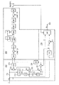
現在の標準規格のアナログテレビジョン送信からディジタル信号に変換するテレビジョン受像機が図1に示されている。アナログ/ディジタル(A/D)変換は本発明の動作では不要である。しかしながら何らかの方法でディジタル信号が生成されなければならない。入力される飛び越し走査ビデオ信号は信号インタフェース部(I/F)11から受信機に入る。この時点で、もしも入力信号が既にディジタルでない場合は、これはA/D変換によってディジタル化される。
【0012】
本発明は入力信号が色空間変換を受ける前でも後でもいずれでも使用することが可能である。飛び越し走査から順次走査(プロスキャン)への変換は、信号のクロミナンス及び輝度(C及びY)成分、または赤緑青(RGB)変換信号のいずれに対しても実施することが可能である。色空間変換は図1の受信機10のインタフェース装置11または処理装置12のいずれかで行なわれる。
【0013】
飛び越し走査からプロスキャンへの変換は、多くの場合処理装置12の中で実施されるが、必要で有ればインタフェース装置11の中で実現することも可能である。何処で変換が行われるかには関係なく、変換された信号は必要に応じてその他の処理を施された後、表示用メモリ14に送られる。主タイミング装置22は処理装置とメモリとの間、並びにメモリと空間光変調器16との間の信号のタイミングを制御する。
【0014】
空間光変調器16は個別に制御可能な素子のx−y配列で構成されている。各々の素子は何らかの型式の駆動回路を有し、これはメモリ14に格納された信号に応答して光源18からの光に作用するように個別の素子に影響を与える。メモリから送信された信号に応答する素子の各々の配列の効果が集積されて画像が形成され、拡大された後画像20の様に現れる。空間光変調器の例としては、液晶素子、及びディジタル式鏡素子等が上げられる。
【0015】
本システムの上記の説明の中で、プロスキャン処理が実現されているが、これはその他の考えられるシステム素子の組み合わせを排他的に除外しているものでは無い。これは単に例として示しただけである。
【0016】
従来型(例えばCRT)モニタとは違って、空間光変調器は画像を走査するためにCRT銃は使用しない。これに代わって、これらはデータの全フレームを一度に表示する、従って入力される飛び越し走査フィールドはひとつのフレームを生成するために一緒にされなければならない。典型的な規格、例えばNTSC及びPALでは、入力フレームは二つのフィールドで入ってくる。例えば、NTSCでは、第一フィールドは偶数番号の走査線を含み、そして第二フィールドは同一フレームの奇数番号の走査線を含む。これを空間光変調器の表面に表示するために、これらのデータはひとつのデータフレームとして一緒にされ、メモリに格納され、そして変調器駆動回路に同時に送信されなければならない。
【0017】
この回路を追加することは空間光変調器を使用するテレビジョンの価格を非常に増加させる。しかしながら、図2−5は本発明のいくつかの実施例を示しており、これはプロスキャンを可能とし、かつ最低限の回路しか必要としないものである。
【0018】
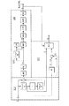
本発明の最低価格での実施例が図2に示されている。全ての処理に対して図示した定義方法は役に立つであろう。フィールド1は現在のフィールド、そしてフィールド0は直前のフィールドである。その処理に於いて生成しようとしている画素はフィールド1内の画素Xである。この処理の中で使用されている画素は画素Aであり、これはフィールド0からの同一走査線上にある。画素B及びCはフィールド1からであり、画素Bは画素Xの上、そして画素Cは画素Xの下である。
【外1】

第一の適用可能なプロスキャン回路は、一般的に画素Xを(A−B)と(A−C)の最小値を探して求めることを実行する。これは図2に図式的に示されている回路で実現される。説明を簡単にするために、この回路は210、230及び250のブロックで表されている三つの機能グループに分割されている。線212上に入力されているデータは画素Cである。グループ210を見ると、水平遅延214の後、線216は画素Bを運んでいる。1フィールドの遅延の後、線220は画素Aを運んでいる。線212(画素C)と線220(画素A)との引き算は226で行われ、その結果の値は222で絶対値に変換される。228に於いて線216(画素B)と線220(画素A)との引き算が実行される。その結果の絶対値が224で得られる。次にこの出力は機能グループ250に入力される。
【0020】
252に於いて比較器または同様の回路素子が使用されて二つの絶対値|A−B|と|A−C|の間の最小値が決定される。システムパラメータに依存する定数が、その結果得られた最小値から引き算される。定数の値は変更可能であり、システムの雑音特性に依存して必要に応じて変更される。非線形演算を実施して雑音に起因する小さな差信号の値を取り除く閾値操作を行う。またこれは差信号の解像度を4ビットに削減する。254で定数を取り除く機能と、256での非線形操作とは一緒に統合することが可能である。その結果得られる非線形操作は図6に示すように図式化できる。
【0021】
データは次にどの画素が水平方向で最大で有るかの判定にかけられるが、これには258の7タップH最大フィルタが用いられる。画素Xでの動き信号の現在値がそのいずれかの側に有る三つの画素と比較される。同様に水平遅延260及び264を用いて、画素Xのいずれかの側の画素が垂直方向で比較され最大値が判定される。第一の比較はMAX268で、その画素とその垂直方向に隣接する画素のひとつとの間で実行される。次に最大値はMAX270に送られ、ここで遅延264からのもう一方の隣接する画素と比較される。MAX機能の目的は、検知される動き信号の範囲を非検出領域まで拡張するにとである。誤った動き検出を避けるために、このデータは次に水平方向低域通過フィルタ(HLPF)272及び垂直方向低域通過フィルタ(VLPF)274に、それぞれ送られる。
【0022】
別の定数がデータから除去され、そしてこれに別の非線形調整が276で行われる。機能グループ250から結果として生じる信号は、線278上の動き信号kである。このデータは機能グループ230の一方の側の混合回路236に送られる。機能グループ230のもう一方の側では、線212上の画素Cの値、遅延232出力の画素Bの値、そして機能グループ210からの画素Aの値が受信されている。画素B及びCは0.5を掛けた後互いに加算される。これらの値は混合回路236に送られ、これは何らかの種類の算術演算回路であり、その結果生じる信号290は、 k(C+B)/2+(1−k)A に等しい。この値はプロスキャン変換の中で画素Xに割り当てられる値である。
【0023】
上記の処理はひとつの処理装置の中で実行されるか、またはその機能をいくつかの処理装置に分散して、欠落した画素Xを求める。この処理を繰り返せばフィールド1内の二本の走査線B並びにCの間の走査線を生成することが可能となる。
これは従ってシステムが飛び越し走査入力を順次走査データに変換して表示することを可能としている。以上説明した対応方法はフィールド差法である。
【0024】
更に高価な別法が図3−5に示されている。価格の上昇はメモリまたは処理能力の増加、またはその両方のためである。図2の機能グループ250に含まれる回路素子は図3でも同様であるので、このブロックは図3に関連して説明する必要はない。機能グループ310及び330はそれぞれ、図2の機能グループ210及び230と僅かに違っている。
【0025】
価格の上昇はこの実施例の中で必要な追加メモリに起因している。画素A,B及びCのみを使用する代わりに、この実施例ではまた画素D及びEをも使用する。画素D及びEはフィールド0からのものであり、画素Aの垂直方向に隣接するもので、画素Dは垂直方向上側に隣接するものそして画素Eは垂直方向下側に隣接するものである。
【外2】
機能グループ310に於いて、入力データはここでも画素Cである。フィールド遅延314を受けたデータは画素Eである。一水平走査線分の遅延後のデータは画素Aである。画素A及びEは0.5を掛け算されて互いに加算される。次に値(A+E)/2が画素Cから324で引き算され、その絶対値が326で求められ、その結果生じる第一値は、|C−(A+E)/2| となる。一方画素Aとなる水平遅延316の出力は、水平遅延320の出力である画素Dと組み合わされる。両方の値とも互いに加算される前に0.5が掛け算される。画素Bの値に対してはその値を引き算し、その結果は、(B−(A+D)/2) となる。その絶対値が求められ、その結果第二値 |B−(A+D)/2| となる。第一並びに第二値は図2の機能グループ250と同一の回路の入力信号となる。
【0027】
このシステムの追加費用は二つの追加された走査線遅延に必要なメモリが原因であるが、走査線メモリを共通に使用して単一の追加走査線メモリをフィールド0に適用し、画素B及びDで使用することも可能である。本実施例の最終出力は更に正確な動き信号kとなる。機能グループ330の混合回路がその結果Xk(C+B)/2+(1−k)AXを出力する場合には、より精密なkの値により画素Xの更に良好な近似が得られる。この回路はこれらの機能を欠落した走査線内の全ての画素に対して実行し、次に全ての走査線に対して繰り返すので、結果として生じるプロスキャンデータは更に良質な画質を有する。
【0028】
図2並びに図3に示すプロスキャンの実施例はプロスキャンのフィールド差実現法であり、図3では強化されたフィールド差法の例を示している。図4はフレーム差実現法を図示する。機能グループ410はひとつのフィールド遅延412を有し、これは前回フィールドを格納して今回フィールドとすることが可能である。これはまた別のフィールド遅延414を有し、これは前々回フィールドを格納する。今まではフィールド1が現在フィールドであって、その中で画素Xを探していた。この実現法ではフィールド2が現在フィールドである。フィールド1は前回フィールド、そしてフィールド0は前々回フィールドである。入力がどのフィールドでも一本置きに飛び越し走査されているため、フィールド0とフィールド2はそれらのなかで同じ線番号、奇数または偶数を有する。
【0029】
機能グループ410は各フィールドの同じ位置に配置されている画素間の差を計算する。例えば、画素Bがフィールド2の走査線4の画素1と仮定すると、その値はフィールド0の走査線4の画素1である画素Jと比較されるはずである。画素Xのいずれかの側に有る二本の線に対するフレーム差が求められ、図2の機能グループ250と同様の機能グループに送られる。これらの回路素子の間の唯一の違いは、追加の水平遅延452が付加されている点である。これは四つの値(フレーム差)の中の最大値を求めるために必要である。この実施例の結果生じるデータは線490に与えられ、更に多くの画素を使用しているので更に良好な画質を提供できる。
【0030】
図2並びに図3と同じ式を用いて、最終データはフィールド1からの画素Aの位置と値とを考慮に入れている。これは画素Aが画素Xと同じ位置に有るため必要である。しかしながら、ひとつの代わりに二つのフィールドのデータの記憶を出来るようにするために十分なメモリを追加し、また追加の水平遅延用に別の走査線データを記憶するために十分なメモリを追加する結果、余分な費用がかさむ。より高い精度はより高いシステム価格の下で得られる。
【0031】
ここで示される物の中で最も高価なプロスキャン実現法が図5に示されている。機能グループ510は機能グループ410と同一である。機能グループ530は機能グループ230、330及び430と同じである。機能グループ450と機能グループ550との違いは、まず最初は追加のフィールド遅延552である。更に定数の加算も取り除かれており、同様に水平遅延走査線の内の二つも除去されている。この実現法、これは時間実現法またはアプローチと呼ばれるは、先行する2フィールドを使用する。現フィールドはここではフィールド3である。付加フィールドを追加することによって更に情報が処理回路に与えられ、画素Xの近似を行う際により高い精度が結果として得られる。しかしながら更に別のフィールドを記憶するためのメモリ追加によってシステム価格は増加する。
【0032】
上記の全てのプロスキャンの実施例は、飛び越し走査から順次走査への変換の必要な機能を実現している。しかしながらもしもシステムがオプションとして特別な特徴、例えばポーズまたは一時停止を持てば、付加される特長は更に明らかとなろう。通常のシステムでは、例えばポーズモードではシステムは指定されたフィールドの再表示を、視聴者がシステムに通常表示を指令するまで継続する。一時停止またはポーズを使用すると、”涙”またはぎざぎざの縁部が画像に生じる。ほとんどのシステムでは欠落したフィールドを生成するために式 k(C+B)/2+(1−k)A を使用しているため、涙現象は動き信号がゼロとなる結果生じる。同じフィールドが再表示されるため、動きは発生しない。
【0033】
上記の実施例では、少なくともひとつの前回フィールドが既に記憶されているので、システムはそのフィールドを使用して二つのフィールドの間を繋ぎ止めることが出来る。これにより表示画像内の涙現象が除去される。
【0034】
本発明の上記の実施例の中で、理想的なシステムとは処理能力の格上げ更新が可能なことであろう。この場合、顧客がセットを購入しようと決めたときに、その顧客は最も安いセットで、先に述べた最も廉価なプロスキャン実現法を購入できる。時間が経っても、顧客はシステムの格上げ更新を、メモリの追加とほとんどソフトウェアで制御されている処理装置の機能変更のみで実施する機会を有する。更に高価なプロスキャン実現法を購入出来る顧客は、追加メモリと既にインストール済みソフトウェアを具備した同一セットを購入出来る。
【0035】
以上のように、可変、モジュール型プロスキャン実現システムの特定の実施例を説明してきたが、これらは添付の特許請求の範囲で規定された部分を除いて本発明の範囲を限定することを意図してそれらの特定の説明がなされたものでは無い。
以上の説明に関して更に以下の項を開示する。
関連する明細書
本明細書は米国特許出願番号第08/429、254(TI−19678)、名称”フィルムモード順次走査変換”と同時に申請されている。
【0036】
(1)飛び越し走査テレビジョン信号を受信するテレビジョンシステムであって:
前記飛び越し走査信号を受信するための受信機と;
前記信号を順次走査データに変換し、前記信号を変換するいくつかの方法のひとつを用いて動作可能な処理装置と;
前記処理装置と通信して、前記変換の途中及び変換の後にデータを受信し、更に多くのメモリを含むように拡張性を有するメモリと;そして
前記変換された信号を順次走査型ビデオ画像として表示するための空間光変調器とを含む、前記システム。
【0037】
(2)第1項記載のシステムに於いて、前記処理装置が前記信号に対してフィールド差を用いて作用する、前記システム。
【0038】
(3)第1項記載のシステムに於いて、前記処理装置が前記信号に対して強化されたフィールド差を用いて作用する、前記システム。
【0039】
(4)第1項記載のシステムに於いて、前記処理装置が前記信号に対してフレーム差を用いて作用する、前記システム。
【0040】
(5)第1項記載のシステムに於いて、前記処理装置が前記信号に対して一時的に作用する、前記システム。
【0041】
(6)第1項記載のシステムに於いて、前記システムが特定モードで二つのフィールドをつなぎ止める機能を有し、その結果人為的な物を削減した静止画像が得られる、前記システム。
【0042】
(7)飛び越し走査から順次走査への変換を具備したテレビジョンシステム(10)である。このシステムは飛び越し走査テレビジョン信号を受信し、次にそれらをそれが使用する実現方法に依存して、フィールド差法、強化型フィールド差法、フレーム差法またはその他の一時処理法のいずれかを使用して順次走査データに変換する。使用される実現方法はどのシステム(10)構成が購入されたかに依存し、更に高価な実現方法に格上げ更新して変更することが可能である。
【図面の簡単な説明】
【図1】空間光変調器を使用したテレビジョンシステムのブロック図を示す。
【図2】フィールド差飛び越し走査を順次走査に変換するための第一実施例を実現するための回路のブロック図を示す。
【図3】フィールド差飛び越し走査を順次走査に変換するための第二実施例を実現するための回路のブロック図を示す。
【図4】フレーム差飛び越し走査を順次走査に変換するための実現回路のブロック図を示す。
【図5】一時フィルタ処理飛び越し走査を順次走査に変換するための実現回路のブロック図を示す。
【図6】図2の256における非線形操作の入出力特性を表わす。
【符号の説明】
10・・・・・・・・受信機
11・・・・・・・・インタフェース装置
12・・・・・・・・処理装置
14・・・・・・・・メモリ
16・・・・・・・・空間光変調器
18・・・・・・・・光源
20・・・・・・・・画像
22・・・・・・・・主タイミング装置
214、232、260、264・・・水平遅延素子
218・・・・・・・フィールド遅延素子
222、224・・・絶対値演算器
226、228、234、254・・・算術演算器
236・・・・・・・混合器
256、276・・・非線形演算素子
272、274・・・低域濾波フィルタ
314・・・・・・・フィールド遅延素子
316、320・・・水平遅延素子
318、322、324・・・算術演算器
326、328・・・絶対値演算器
412、414・・・フィールド遅延素子
452・・・・・・・フィールド遅延素子
552・・・・・・・フィールド遅延素子[0001]
BACKGROUND OF THE INVENTION
The present invention relates to a television system, and more particularly to a progressive scanning digital television system.
[0002]
[Prior art]
Broadcast television signals usually arrive at the receiver in an interlaced format. That is, each video frame to be displayed arrives as two fields. The first field contains either even numbered scan lines or odd numbered scan lines. The second field contains the opposite set of scan lines.
[0003]
The television displays these frames so that the viewer does not actually know that they are two fields. However, as a result of recent innovations in the field of broadcast television, scanning has begun sequentially. In progressive scanning (pro-scan), interlaced fields are combined before display, and all frames are displayed. In cathode ray tube (CRT) television, this means that one or more electron guns that scan the image instead of scanning odd or even scan lines first and then scan the opposite scan lines. Means to scan all frames.
[0004]
Some embodiments of television systems do not use CRT. These televisions use an array of individually controllable elements such as liquid crystal elements or digital micromirror elements (LCD or DMD, respectively). Since these systems do not have a scanning gun, the interlace scanning of the field must normally be canceled and all frames must be input to the drive circuit of the array of individual elements before display.
[0005]
This raises the problem of raising the system price and requiring high-level circuitry to perform these functions. However, without the ability to implement proscan, other advantages of using a spatial light modulator, such as a fully digital television (digital from input to output) as well as clear images with excellent resolution, Hazy because of the high price.
[0006]
[Problems to be solved by the invention]
Therefore, there is a need for a method for converting from interlaced scanning to proscanning in a system that uses a spatial light modulator without significantly increasing system cost.
[0007]
[Means for Solving the Problems]
A television system for receiving interlaced scanning signals is disclosed. The system receives the interlaced scan signal and converts it to progressive scan data using one of several processing methods, depending on the configuration of the system to be purchased next. The configuration varies depending on the price, but can be upgraded and updated easily to include more expensive processing methods.
[0008]
The feature of this system is that it makes it easier for manufacturers to acquire more customers by providing one system to a wide range of buyers.
[0009]
The feature of this system is that it can easily incorporate upgrade updates by including all of the processing power required to implement a more complex method of converting from interlaced scanning to sequential scanning.
[0010]
For a more complete understanding of the present invention, as well as further features, the following detailed description is set forth with reference to the accompanying drawings.
[0011]
DETAILED DESCRIPTION OF THE INVENTION
A television receiver for converting a current standard analog television transmission into a digital signal is shown in FIG. Analog / digital (A / D) conversion is not required in the operation of the present invention. However, the digital signal must be generated in some way. The input interlaced scanning video signal enters the receiver from the signal interface unit (I / F) 11. At this point, if the input signal is not already digital, it is digitized by A / D conversion.
[0012]
The present invention can be used either before or after the input signal undergoes color space conversion. The conversion from interlaced scanning to progressive scanning (proscan) can be performed on either the chrominance and luminance (C and Y) components of the signal or the red-green-blue (RGB) conversion signal. The color space conversion is performed by either the interface device 11 or the
[0013]
In many cases, the conversion from the interlaced scanning to the pro-scan is performed in the
[0014]
The
[0015]
In the above description of the system, a proscan process is realized, but this does not exclude other possible combinations of system elements. This is only given as an example.
[0016]
Unlike conventional (eg, CRT) monitors, spatial light modulators do not use CRT guns to scan images. Instead, they display all the frames of data at once, so the interlaced scan fields that are input must be combined to produce one frame. In typical standards, such as NTSC and PAL, an input frame comes in two fields. For example, in NTSC, the first field contains even numbered scan lines and the second field contains odd numbered scan lines of the same frame. In order to display this on the surface of the spatial light modulator, these data must be combined as one data frame, stored in memory, and transmitted simultaneously to the modulator driver circuit.
[0017]
The addition of this circuit greatly increases the price of televisions that use spatial light modulators. However, FIGS. 2-5 show some embodiments of the present invention that allow proscan and require minimal circuitry.
[0018]
The lowest price embodiment of the present invention is shown in FIG. The illustrated definition method will be useful for all processes.
[Outside 1]
The first applicable proscan circuit generally performs a search for the pixel X by searching for the minimum values of (A-B) and (A-C). This is achieved with the circuit schematically shown in FIG. For simplicity of explanation, the circuit is divided into three functional groups represented by
[0020]
At 252 a comparator or similar circuit element is used to determine the minimum value between the two absolute values | A-B | and | A-C |. A constant that depends on the system parameters is subtracted from the resulting minimum value. The value of the constant can be changed and is changed as necessary depending on the noise characteristics of the system. A threshold operation is performed to remove a small difference signal value caused by noise by performing a non-linear operation. This also reduces the resolution of the difference signal to 4 bits. The function of removing constants at 254 and the non-linear operation at 256 can be integrated together. The resulting nonlinear operation can be schematized as shown in FIG.
[0021]
The data is then subjected to a determination of which pixels are maximal in the horizontal direction, using a 258 7-tap H maximum filter. The current value of the motion signal at pixel X is compared with the three pixels on either side. Similarly, using the
[0022]
Another constant is removed from the data and another non-linear adjustment is made at 276 to this. The resulting signal from
[0023]
The above processing is executed in one processing device, or the function is distributed to several processing devices to find the missing pixel X. If this process is repeated, a scanning line between two scanning lines B and C in the
This therefore allows the system to display the interlaced scan input converted to progressive scan data. The correspondence method described above is the field difference method.
[0024]
A more expensive alternative is shown in FIGS. 3-5. The increase in price is due to increased memory and / or processing power. Since the circuit elements included in the
[0025]
The increase in price is due to the additional memory required in this embodiment. Instead of using only pixels A, B and C, this embodiment also uses pixels D and E. Pixels D and E are from
[Outside 2]
In
[0027]
The additional cost of this system is due to the memory required for the two additional scan line delays, but the scan line memory is used in common and a single additional scan line memory is applied to
[0028]
2 and 3 are examples of the pro-scan field difference realization method, and FIG. 3 shows an example of the enhanced field difference method. FIG. 4 illustrates a frame difference realization method. The
[0029]
The
[0030]
Using the same equations as in FIGS. 2 and 3, the final data takes into account the position and value of pixel A from
[0031]
The most expensive proscan implementation of the one shown here is shown in FIG. The
[0032]
All of the above proscan embodiments implement the necessary functions of conversion from interlaced scanning to sequential scanning. However, if the system optionally has special features such as pauses or pauses, the added features will become more apparent. In a normal system, for example in pause mode, the system continues to redisplay the specified field until the viewer commands the system to display normally. Using pauses or pauses creates “tears” or jagged edges in the image. Since most systems use the equation k (C + B) / 2 + (1-k) A to generate the missing field, the tear phenomenon results from the motion signal being zero. Since the same field is redisplayed, no movement occurs.
[0033]
In the above embodiment, since at least one previous field has already been stored, the system can use that field to bridge between the two fields. Thereby, the tear phenomenon in the display image is removed.
[0034]
Among the above embodiments of the present invention, an ideal system would be capable of upgrading and updating processing power. In this case, when a customer decides to purchase a set, the customer can purchase the cheapest proscan implementation described above with the cheapest set. Over time, customers have the opportunity to upgrade their system upgrades with only the addition of memory and functional changes to processing devices that are mostly controlled by software. Customers who can purchase more expensive proscan implementations can purchase the same set with additional memory and already installed software.
[0035]
While specific embodiments of variable, modular proscan implementation systems have been described above, they are intended to limit the scope of the invention except as defined in the appended claims. And that specific explanation is not made.
The following items are further disclosed with respect to the above description.
Related Specification This specification is filed concurrently with US patent application Ser. No. 08 / 429,254 (TI-19678), entitled “Film Mode Sequential Scan Conversion”.
[0036]
(1) A television system for receiving interlaced scanning television signals:
A receiver for receiving the interlaced scanning signal;
A processor that converts the signal into progressive scan data and is operable using one of several methods for converting the signal;
A memory that communicates with the processing device, receives data during and after the conversion, and has expandability to include more memory; and displays the converted signal as a progressively scanned video image And said spatial light modulator.
[0037]
(2) The system according to (1), wherein the processing device acts on the signal using a field difference.
[0038]
(3) The system of
[0039]
(4) The system according to (1), wherein the processing device operates on the signal using a frame difference.
[0040]
(5) The system according to (1), wherein the processing device temporarily acts on the signal.
[0041]
(6) The system according to
[0042]
(7) A television system (10) having conversion from interlaced scanning to sequential scanning. This system receives interlaced scanning television signals and then uses either the field difference method, the enhanced field difference method, the frame difference method, or other temporal processing methods, depending on the implementation that it uses. Use to convert to sequential scan data. The implementation method used depends on which system (10) configuration is purchased and can be upgraded and updated to a more expensive implementation method.
[Brief description of the drawings]
FIG. 1 shows a block diagram of a television system using a spatial light modulator.
FIG. 2 shows a block diagram of a circuit for realizing a first embodiment for converting field difference interlaced scanning into sequential scanning.
FIG. 3 shows a block diagram of a circuit for realizing a second embodiment for converting a field difference interlaced scanning into a sequential scanning.
FIG. 4 shows a block diagram of an implementation circuit for converting frame difference interlaced scanning into sequential scanning.
FIG. 5 shows a block diagram of an implementation circuit for converting temporary filter processing interlaced scanning into sequential scanning.
6 represents the input / output characteristics of the nonlinear operation at 256 in FIG.
[Explanation of symbols]
10 ... Receiver 11 ...
Claims (1)
1)前記飛び越し走査信号を受信するための受信機と;
2)前記信号内の画素を順次走査画素データに変換する処理装置であって、前記信号を変換するいくつかの方法の内のひとつを用いて、前記処理装置が、前記複数の方法において少なくとも二つのビデオデータ間で動き検出を実行するように動作可能であり、
2)−1:画素データ間で変換を行う前記複数の方法のうちの少なくとも一つの第一の方法は、第一の相対位置の組の中にある画素データに対応するものであり、
2)−2:画素データ間で変換を行う前記複数の方法のうちの少なくとも一つの第二の方法は、前記第一の相対位置の組とは異なる、第二の相対位置の組の中にある画素データに対応するものである、前記処理装置と:
3)前記処理装置と通信し、前記変換の途中及び変換の後にデータを受信し、更に多くのメモリを含むように拡張性を有するメモリであって、前記メモリの拡張は、前記複数の方法の追加に備えるものであり、また前記メモリの拡張は、前記追加された方法のどれが可能かを決定するものである、前記メモリと;
4)前記変換された信号を順次走査型ビデオ画像として表示するための空間光変調器とを含む、前記システム。A television system for receiving interlaced scanning television signals:
1) a receiver for receiving the interlaced scanning signal;
2) A processing device for converting pixels in the signal into sequentially scanned pixel data, using one of several methods for converting the signal, wherein the processing device is at least two in the plurality of methods. Is operable to perform motion detection between two video data,
2) -1: At least one of the plurality of methods for performing conversion between pixel data corresponds to pixel data in the first set of relative positions,
2) -2: At least one second method of the plurality of methods for performing conversion between pixel data is different from the first set of relative positions in the second set of relative positions. The processing device corresponding to certain pixel data:
3) A memory that communicates with the processing device, receives data during and after the conversion, and has more expandability to include more memories, and the expansion of the memory is performed by the plurality of methods. In addition to the memory, wherein the expansion of the memory is to determine which of the added methods is possible;
4) A spatial light modulator for displaying the converted signal as a progressive scan video image.
Applications Claiming Priority (2)
| Application Number | Priority Date | Filing Date | Title |
|---|---|---|---|
| US43077495A | 1995-04-27 | 1995-04-27 | |
| US430774 | 1995-04-27 |
Publications (2)
| Publication Number | Publication Date |
|---|---|
| JPH09102935A JPH09102935A (en) | 1997-04-15 |
| JP4335979B2 true JP4335979B2 (en) | 2009-09-30 |
Family
ID=23708964
Family Applications (1)
| Application Number | Title | Priority Date | Filing Date |
|---|---|---|---|
| JP14339396A Expired - Fee Related JP4335979B2 (en) | 1995-04-27 | 1996-04-30 | Low cost progressive scan television system with special features |
Country Status (5)
| Country | Link |
|---|---|
| US (1) | US6320620B1 (en) |
| EP (1) | EP0740468B1 (en) |
| JP (1) | JP4335979B2 (en) |
| KR (1) | KR960039839A (en) |
| DE (1) | DE69619430T2 (en) |
Families Citing this family (5)
| Publication number | Priority date | Publication date | Assignee | Title |
|---|---|---|---|---|
| GB9703107D0 (en) | 1997-02-14 | 1997-04-02 | Digital Projection Ltd | Display device |
| AU6511899A (en) * | 1999-06-17 | 2001-01-09 | 3M Innovative Properties Company | Freeze-frame function in an electronic projection system |
| US7375760B2 (en) * | 2001-12-31 | 2008-05-20 | Texas Instruments Incorporated | Content-dependent scan rate converter with adaptive noise reduction |
| JP4390506B2 (en) * | 2003-09-02 | 2009-12-24 | 三洋電機株式会社 | Horizontal contour correction circuit |
| US8280183B2 (en) * | 2008-06-05 | 2012-10-02 | Texas Instruments Incorporated | Noise robust contrast-enhancement engine employing IIR filters |
Family Cites Families (10)
| Publication number | Priority date | Publication date | Assignee | Title |
|---|---|---|---|---|
| US4215397A (en) | 1978-08-24 | 1980-07-29 | Texas Instruments Incorporated | Automatic end-of-scan control system for a programmable process controller with expandable memory |
| US5192946A (en) * | 1989-02-27 | 1993-03-09 | Texas Instruments Incorporated | Digitized color video display system |
| JP2732650B2 (en) * | 1989-02-28 | 1998-03-30 | 株式会社東芝 | Vertical edge detection circuit |
| US5095354A (en) | 1989-09-01 | 1992-03-10 | Matsushita Electric Industrial Co., Ltd. | Scanning format converter with motion compensation |
| US5027201A (en) * | 1989-12-21 | 1991-06-25 | Rca Licensing Corporation | Motion detection apparatus as for an interlace to non-interlace scan converter |
| JP3187851B2 (en) | 1990-03-01 | 2001-07-16 | テキサス インスツルメンツ インコーポレイテツド | TV with improved clarity |
| JP3271143B2 (en) * | 1990-10-22 | 2002-04-02 | ソニー株式会社 | Video signal processing circuit |
| US5291280A (en) * | 1992-05-05 | 1994-03-01 | Faroudja Y C | Motion detection between even and odd fields within 2:1 interlaced television standard |
| DE69332302T2 (en) * | 1992-11-23 | 2003-01-30 | Thomson Multimedia Sa | Method and device for adaptive conversion into a line sequence signal |
| US5398071A (en) | 1993-11-02 | 1995-03-14 | Texas Instruments Incorporated | Film-to-video format detection for digital television |
-
1996
- 1996-04-19 US US08/635,449 patent/US6320620B1/en not_active Expired - Lifetime
- 1996-04-27 KR KR1019960013338A patent/KR960039839A/en not_active Application Discontinuation
- 1996-04-29 DE DE69619430T patent/DE69619430T2/en not_active Expired - Lifetime
- 1996-04-29 EP EP96106768A patent/EP0740468B1/en not_active Expired - Lifetime
- 1996-04-30 JP JP14339396A patent/JP4335979B2/en not_active Expired - Fee Related
Also Published As
| Publication number | Publication date |
|---|---|
| KR960039839A (en) | 1996-11-25 |
| EP0740468A1 (en) | 1996-10-30 |
| US6320620B1 (en) | 2001-11-20 |
| JPH09102935A (en) | 1997-04-15 |
| EP0740468B1 (en) | 2002-02-27 |
| DE69619430T2 (en) | 2002-10-10 |
| DE69619430D1 (en) | 2002-04-04 |
Similar Documents
| Publication | Publication Date | Title |
|---|---|---|
| US6239842B1 (en) | Method of de-interlacing video signals using a mixed mode spatial and temporal approximation technique | |
| KR100261638B1 (en) | Video System and Method of Using Same | |
| EP0700015A1 (en) | Image scaling using cubic filters | |
| JPH0846927A (en) | Generation of frame pixel data | |
| JPH0884321A (en) | Video data processing method | |
| US8280190B2 (en) | Image display device, image processing circuit, and image processing method | |
| JP4435871B2 (en) | RGB / YUV convolution system | |
| JP2003018500A (en) | Image processing circuit, image display device, and an image processing method | |
| JPH11146349A (en) | Image converter and image conversion method | |
| JP4335979B2 (en) | Low cost progressive scan television system with special features | |
| EP0721640A1 (en) | Flat panel image reconstruction interface | |
| KR20030097507A (en) | Color calibrator for flat panel display and method thereof | |
| JP3251487B2 (en) | Image processing device | |
| EP1600005B1 (en) | Processing signals for a color sequential display | |
| JP2003069859A (en) | Moving image processing adapting to motion | |
| JP2002108298A (en) | Digital signal processing circuit, its processing method, display device, liquid crystal display device and liquid crystal projector | |
| US5581306A (en) | Vertical scaling for digital image data with aperture correction | |
| JPH08317321A (en) | Image display device | |
| WO2003083559A2 (en) | Color non-uniformity alignment for light engines | |
| JP3347234B2 (en) | Liquid crystal display | |
| JPH07129125A (en) | Picture element arrangement display device | |
| KR20050097549A (en) | Processing picture signals for a color sequential display | |
| JPH0678251A (en) | Matrix video display device | |
| JPH11338406A (en) | Sampling phase adjusting device | |
| KR19990050860A (en) | Camera's spatial resolution enhancement device |
Legal Events
| Date | Code | Title | Description |
|---|---|---|---|
| A131 | Notification of reasons for refusal |
Free format text: JAPANESE INTERMEDIATE CODE: A131 Effective date: 20060516 |
|
| A601 | Written request for extension of time |
Free format text: JAPANESE INTERMEDIATE CODE: A601 Effective date: 20060816 |
|
| A602 | Written permission of extension of time |
Free format text: JAPANESE INTERMEDIATE CODE: A602 Effective date: 20060821 |
|
| A521 | Written amendment |
Free format text: JAPANESE INTERMEDIATE CODE: A523 Effective date: 20061116 |
|
| A131 | Notification of reasons for refusal |
Free format text: JAPANESE INTERMEDIATE CODE: A131 Effective date: 20080304 |
|
| A601 | Written request for extension of time |
Free format text: JAPANESE INTERMEDIATE CODE: A601 Effective date: 20080602 |
|
| A602 | Written permission of extension of time |
Free format text: JAPANESE INTERMEDIATE CODE: A602 Effective date: 20080605 |
|
| A601 | Written request for extension of time |
Free format text: JAPANESE INTERMEDIATE CODE: A601 Effective date: 20080704 |
|
| A602 | Written permission of extension of time |
Free format text: JAPANESE INTERMEDIATE CODE: A602 Effective date: 20080709 |
|
| A601 | Written request for extension of time |
Free format text: JAPANESE INTERMEDIATE CODE: A601 Effective date: 20080804 |
|
| A602 | Written permission of extension of time |
Free format text: JAPANESE INTERMEDIATE CODE: A602 Effective date: 20080807 |
|
| A521 | Written amendment |
Free format text: JAPANESE INTERMEDIATE CODE: A523 Effective date: 20080902 |
|
| TRDD | Decision of grant or rejection written | ||
| A01 | Written decision to grant a patent or to grant a registration (utility model) |
Free format text: JAPANESE INTERMEDIATE CODE: A01 Effective date: 20090609 |
|
| A01 | Written decision to grant a patent or to grant a registration (utility model) |
Free format text: JAPANESE INTERMEDIATE CODE: A01 |
|
| A61 | First payment of annual fees (during grant procedure) |
Free format text: JAPANESE INTERMEDIATE CODE: A61 Effective date: 20090626 |
|
| FPAY | Renewal fee payment (event date is renewal date of database) |
Free format text: PAYMENT UNTIL: 20120703 Year of fee payment: 3 |
|
| R150 | Certificate of patent or registration of utility model |
Free format text: JAPANESE INTERMEDIATE CODE: R150 |
|
| FPAY | Renewal fee payment (event date is renewal date of database) |
Free format text: PAYMENT UNTIL: 20130703 Year of fee payment: 4 |
|
| R250 | Receipt of annual fees |
Free format text: JAPANESE INTERMEDIATE CODE: R250 |
|
| LAPS | Cancellation because of no payment of annual fees |