JP4332787B2 - 回路設計装置および方法、記録媒体、プログラム、並びに半導体集積回路 - Google Patents
回路設計装置および方法、記録媒体、プログラム、並びに半導体集積回路 Download PDFInfo
- Publication number
- JP4332787B2 JP4332787B2 JP2003404063A JP2003404063A JP4332787B2 JP 4332787 B2 JP4332787 B2 JP 4332787B2 JP 2003404063 A JP2003404063 A JP 2003404063A JP 2003404063 A JP2003404063 A JP 2003404063A JP 4332787 B2 JP4332787 B2 JP 4332787B2
- Authority
- JP
- Japan
- Prior art keywords
- signal
- bit
- processing
- wiring
- circuit
- Prior art date
- Legal status (The legal status is an assumption and is not a legal conclusion. Google has not performed a legal analysis and makes no representation as to the accuracy of the status listed.)
- Expired - Fee Related
Links
Images


Landscapes
- Semiconductor Integrated Circuits (AREA)
- Design And Manufacture Of Integrated Circuits (AREA)
Priority Applications (1)
| Application Number | Priority Date | Filing Date | Title |
|---|---|---|---|
| JP2003404063A JP4332787B2 (ja) | 2003-12-03 | 2003-12-03 | 回路設計装置および方法、記録媒体、プログラム、並びに半導体集積回路 |
Applications Claiming Priority (1)
| Application Number | Priority Date | Filing Date | Title |
|---|---|---|---|
| JP2003404063A JP4332787B2 (ja) | 2003-12-03 | 2003-12-03 | 回路設計装置および方法、記録媒体、プログラム、並びに半導体集積回路 |
Publications (3)
| Publication Number | Publication Date |
|---|---|
| JP2005165706A JP2005165706A (ja) | 2005-06-23 |
| JP2005165706A5 JP2005165706A5 (https=) | 2006-12-28 |
| JP4332787B2 true JP4332787B2 (ja) | 2009-09-16 |
Family
ID=34727141
Family Applications (1)
| Application Number | Title | Priority Date | Filing Date |
|---|---|---|---|
| JP2003404063A Expired - Fee Related JP4332787B2 (ja) | 2003-12-03 | 2003-12-03 | 回路設計装置および方法、記録媒体、プログラム、並びに半導体集積回路 |
Country Status (1)
| Country | Link |
|---|---|
| JP (1) | JP4332787B2 (https=) |
-
2003
- 2003-12-03 JP JP2003404063A patent/JP4332787B2/ja not_active Expired - Fee Related
Also Published As
| Publication number | Publication date |
|---|---|
| JP2005165706A (ja) | 2005-06-23 |
Similar Documents
| Publication | Publication Date | Title |
|---|---|---|
| JP3461443B2 (ja) | 半導体装置、半導体装置の設計方法、記録媒体および半導体装置の設計支援装置 | |
| US8487658B2 (en) | Compact and robust level shifter layout design | |
| US11971740B2 (en) | Timing error detection and correction circuit | |
| CN103577626B (zh) | 带有具有用于访问寄存器的输入和输出旁通路径的逻辑区域的集成电路 | |
| US20010029599A1 (en) | Method and apparatus for clock gated logic circuits to reduce electric power consumption | |
| JPH09162720A (ja) | 組み合わせ論理回路及びその設計方法 | |
| US20110320989A1 (en) | Minimal leakage-power standard cell library | |
| US6618847B1 (en) | Power stabilizer using under-utilized standard cells | |
| US10762270B2 (en) | Clock tree synthesis method | |
| CN115238637A (zh) | 多阈值标准单元库设计方法及多阈值标准单元库 | |
| US20100231256A1 (en) | Spare cell library design for integrated circuit | |
| JP3629250B2 (ja) | 半導体集積回路のレイアウト方法及び半導体集積回路 | |
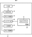
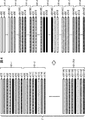
| JP4332787B2 (ja) | 回路設計装置および方法、記録媒体、プログラム、並びに半導体集積回路 | |
| US6185720B1 (en) | Slaveless synchronous system design | |
| US7409657B2 (en) | Clock tree layout method for semiconductor integrated circuit | |
| JP2009218877A (ja) | カウンター回路 | |
| TWI897516B (zh) | 積體電路佈局及其產生的方法 | |
| JP2972719B2 (ja) | 半導体集積回路装置及びその配置方法 | |
| CN120124542A (zh) | 芯片设计中的功耗优化方法、装置、电子设备及存储介质 | |
| JP2006085362A (ja) | 論理回路、クロックスキュー削減システム、及びクロックスキュー削減方法 | |
| JP4211264B2 (ja) | 半導体装置及びその設計方法 | |
| JP2004158484A (ja) | 設計方法、設計装置、記録媒体、プログラム、および半導体集積回路 | |
| JP3012630B1 (ja) | 半導体集積回路におけるクロック配線方法 | |
| US20040210689A1 (en) | Timing information generating apparatus | |
| EP1814152A1 (en) | Semiconductor integrated circuit wiring design system, semiconductor integrated circuit, and wiring design program |
Legal Events
| Date | Code | Title | Description |
|---|---|---|---|
| A521 | Written amendment |
Free format text: JAPANESE INTERMEDIATE CODE: A523 Effective date: 20061110 |
|
| A621 | Written request for application examination |
Free format text: JAPANESE INTERMEDIATE CODE: A621 Effective date: 20061110 |
|
| A131 | Notification of reasons for refusal |
Free format text: JAPANESE INTERMEDIATE CODE: A131 Effective date: 20090303 |
|
| A521 | Written amendment |
Free format text: JAPANESE INTERMEDIATE CODE: A523 Effective date: 20090501 |
|
| TRDD | Decision of grant or rejection written | ||
| A01 | Written decision to grant a patent or to grant a registration (utility model) |
Free format text: JAPANESE INTERMEDIATE CODE: A01 Effective date: 20090528 |
|
| A01 | Written decision to grant a patent or to grant a registration (utility model) |
Free format text: JAPANESE INTERMEDIATE CODE: A01 |
|
| A61 | First payment of annual fees (during grant procedure) |
Free format text: JAPANESE INTERMEDIATE CODE: A61 Effective date: 20090610 |
|
| FPAY | Renewal fee payment (event date is renewal date of database) |
Free format text: PAYMENT UNTIL: 20120703 Year of fee payment: 3 |
|
| FPAY | Renewal fee payment (event date is renewal date of database) |
Free format text: PAYMENT UNTIL: 20120703 Year of fee payment: 3 |
|
| LAPS | Cancellation because of no payment of annual fees |