JP4331663B2 - Thin film coil, coil drive circuit, and magnetic head - Google Patents
Thin film coil, coil drive circuit, and magnetic head Download PDFInfo
- Publication number
- JP4331663B2 JP4331663B2 JP2004272190A JP2004272190A JP4331663B2 JP 4331663 B2 JP4331663 B2 JP 4331663B2 JP 2004272190 A JP2004272190 A JP 2004272190A JP 2004272190 A JP2004272190 A JP 2004272190A JP 4331663 B2 JP4331663 B2 JP 4331663B2
- Authority
- JP
- Japan
- Prior art keywords
- layer
- coil
- spiral
- spiral coils
- peripheral end
- Prior art date
- Legal status (The legal status is an assumption and is not a legal conclusion. Google has not performed a legal analysis and makes no representation as to the accuracy of the status listed.)
- Expired - Fee Related
Links
Images


Classifications
-
- G—PHYSICS
- G11—INFORMATION STORAGE
- G11B—INFORMATION STORAGE BASED ON RELATIVE MOVEMENT BETWEEN RECORD CARRIER AND TRANSDUCER
- G11B11/00—Recording on or reproducing from the same record carrier wherein for these two operations the methods are covered by different main groups of groups G11B3/00 - G11B7/00 or by different subgroups of group G11B9/00; Record carriers therefor
- G11B11/10—Recording on or reproducing from the same record carrier wherein for these two operations the methods are covered by different main groups of groups G11B3/00 - G11B7/00 or by different subgroups of group G11B9/00; Record carriers therefor using recording by magnetic means or other means for magnetisation or demagnetisation of a record carrier, e.g. light induced spin magnetisation; Demagnetisation by thermal or stress means in the presence or not of an orienting magnetic field
- G11B11/105—Recording on or reproducing from the same record carrier wherein for these two operations the methods are covered by different main groups of groups G11B3/00 - G11B7/00 or by different subgroups of group G11B9/00; Record carriers therefor using recording by magnetic means or other means for magnetisation or demagnetisation of a record carrier, e.g. light induced spin magnetisation; Demagnetisation by thermal or stress means in the presence or not of an orienting magnetic field using a beam of light or a magnetic field for recording by change of magnetisation and a beam of light for reproducing, i.e. magneto-optical, e.g. light-induced thermomagnetic recording, spin magnetisation recording, Kerr or Faraday effect reproducing
- G11B11/10532—Heads
- G11B11/10534—Heads for recording by magnetising, demagnetising or transfer of magnetisation, by radiation, e.g. for thermomagnetic recording
-
- G—PHYSICS
- G11—INFORMATION STORAGE
- G11B—INFORMATION STORAGE BASED ON RELATIVE MOVEMENT BETWEEN RECORD CARRIER AND TRANSDUCER
- G11B5/00—Recording by magnetisation or demagnetisation of a record carrier; Reproducing by magnetic means; Record carriers therefor
- G11B5/127—Structure or manufacture of heads, e.g. inductive
- G11B5/17—Construction or disposition of windings
-
- G—PHYSICS
- G11—INFORMATION STORAGE
- G11B—INFORMATION STORAGE BASED ON RELATIVE MOVEMENT BETWEEN RECORD CARRIER AND TRANSDUCER
- G11B5/00—Recording by magnetisation or demagnetisation of a record carrier; Reproducing by magnetic means; Record carriers therefor
- G11B5/127—Structure or manufacture of heads, e.g. inductive
- G11B5/31—Structure or manufacture of heads, e.g. inductive using thin films
- G11B5/3109—Details
- G11B5/313—Disposition of layers
- G11B5/3133—Disposition of layers including layers not usually being a part of the electromagnetic transducer structure and providing additional features, e.g. for improving heat radiation, reduction of power dissipation, adaptations for measurement or indication of gap depth or other properties of the structure
-
- G—PHYSICS
- G11—INFORMATION STORAGE
- G11B—INFORMATION STORAGE BASED ON RELATIVE MOVEMENT BETWEEN RECORD CARRIER AND TRANSDUCER
- G11B11/00—Recording on or reproducing from the same record carrier wherein for these two operations the methods are covered by different main groups of groups G11B3/00 - G11B7/00 or by different subgroups of group G11B9/00; Record carriers therefor
- G11B11/10—Recording on or reproducing from the same record carrier wherein for these two operations the methods are covered by different main groups of groups G11B3/00 - G11B7/00 or by different subgroups of group G11B9/00; Record carriers therefor using recording by magnetic means or other means for magnetisation or demagnetisation of a record carrier, e.g. light induced spin magnetisation; Demagnetisation by thermal or stress means in the presence or not of an orienting magnetic field
- G11B11/105—Recording on or reproducing from the same record carrier wherein for these two operations the methods are covered by different main groups of groups G11B3/00 - G11B7/00 or by different subgroups of group G11B9/00; Record carriers therefor using recording by magnetic means or other means for magnetisation or demagnetisation of a record carrier, e.g. light induced spin magnetisation; Demagnetisation by thermal or stress means in the presence or not of an orienting magnetic field using a beam of light or a magnetic field for recording by change of magnetisation and a beam of light for reproducing, i.e. magneto-optical, e.g. light-induced thermomagnetic recording, spin magnetisation recording, Kerr or Faraday effect reproducing
- G11B11/10502—Recording on or reproducing from the same record carrier wherein for these two operations the methods are covered by different main groups of groups G11B3/00 - G11B7/00 or by different subgroups of group G11B9/00; Record carriers therefor using recording by magnetic means or other means for magnetisation or demagnetisation of a record carrier, e.g. light induced spin magnetisation; Demagnetisation by thermal or stress means in the presence or not of an orienting magnetic field using a beam of light or a magnetic field for recording by change of magnetisation and a beam of light for reproducing, i.e. magneto-optical, e.g. light-induced thermomagnetic recording, spin magnetisation recording, Kerr or Faraday effect reproducing characterised by the transducing operation to be executed
- G11B11/10504—Recording
- G11B11/10508—Recording by modulating only the magnetic field at the transducer
-
- G—PHYSICS
- G11—INFORMATION STORAGE
- G11B—INFORMATION STORAGE BASED ON RELATIVE MOVEMENT BETWEEN RECORD CARRIER AND TRANSDUCER
- G11B11/00—Recording on or reproducing from the same record carrier wherein for these two operations the methods are covered by different main groups of groups G11B3/00 - G11B7/00 or by different subgroups of group G11B9/00; Record carriers therefor
- G11B11/10—Recording on or reproducing from the same record carrier wherein for these two operations the methods are covered by different main groups of groups G11B3/00 - G11B7/00 or by different subgroups of group G11B9/00; Record carriers therefor using recording by magnetic means or other means for magnetisation or demagnetisation of a record carrier, e.g. light induced spin magnetisation; Demagnetisation by thermal or stress means in the presence or not of an orienting magnetic field
- G11B11/105—Recording on or reproducing from the same record carrier wherein for these two operations the methods are covered by different main groups of groups G11B3/00 - G11B7/00 or by different subgroups of group G11B9/00; Record carriers therefor using recording by magnetic means or other means for magnetisation or demagnetisation of a record carrier, e.g. light induced spin magnetisation; Demagnetisation by thermal or stress means in the presence or not of an orienting magnetic field using a beam of light or a magnetic field for recording by change of magnetisation and a beam of light for reproducing, i.e. magneto-optical, e.g. light-induced thermomagnetic recording, spin magnetisation recording, Kerr or Faraday effect reproducing
- G11B11/1055—Disposition or mounting of transducers relative to record carriers
- G11B11/10552—Arrangements of transducers relative to each other, e.g. coupled heads, optical and magnetic head on the same base
- G11B11/10554—Arrangements of transducers relative to each other, e.g. coupled heads, optical and magnetic head on the same base the transducers being disposed on the same side of the carrier
-
- G—PHYSICS
- G11—INFORMATION STORAGE
- G11B—INFORMATION STORAGE BASED ON RELATIVE MOVEMENT BETWEEN RECORD CARRIER AND TRANSDUCER
- G11B11/00—Recording on or reproducing from the same record carrier wherein for these two operations the methods are covered by different main groups of groups G11B3/00 - G11B7/00 or by different subgroups of group G11B9/00; Record carriers therefor
- G11B11/10—Recording on or reproducing from the same record carrier wherein for these two operations the methods are covered by different main groups of groups G11B3/00 - G11B7/00 or by different subgroups of group G11B9/00; Record carriers therefor using recording by magnetic means or other means for magnetisation or demagnetisation of a record carrier, e.g. light induced spin magnetisation; Demagnetisation by thermal or stress means in the presence or not of an orienting magnetic field
- G11B11/105—Recording on or reproducing from the same record carrier wherein for these two operations the methods are covered by different main groups of groups G11B3/00 - G11B7/00 or by different subgroups of group G11B9/00; Record carriers therefor using recording by magnetic means or other means for magnetisation or demagnetisation of a record carrier, e.g. light induced spin magnetisation; Demagnetisation by thermal or stress means in the presence or not of an orienting magnetic field using a beam of light or a magnetic field for recording by change of magnetisation and a beam of light for reproducing, i.e. magneto-optical, e.g. light-induced thermomagnetic recording, spin magnetisation recording, Kerr or Faraday effect reproducing
- G11B11/1055—Disposition or mounting of transducers relative to record carriers
- G11B11/1058—Flying heads
Landscapes
- Engineering & Computer Science (AREA)
- Manufacturing & Machinery (AREA)
- Physics & Mathematics (AREA)
- Electromagnetism (AREA)
- Magnetic Heads (AREA)
- Coils Or Transformers For Communication (AREA)
Description
本願発明は、磁気記録媒体へのデータの記録を行なうのに用いられる薄膜コイル、コイル駆動回路、および磁気ヘッドに関する。 The present invention relates to a thin film coil, a coil drive circuit, and a magnetic head used for recording data on a magnetic recording medium.
磁気記録媒体へのデータの記録は、磁気ヘッドに備えられた薄膜コイルで発生する記録用磁界の磁束方向を制御することにより行なわれる。この記録用磁界の磁気記録媒体に対する磁束方向は、上記薄膜コイルを駆動することで急峻かつ連続的に反転させられる。磁気記録媒体には、磁束方向をできる限り高速に反転しながら記録用磁界を作用させることが好ましいため、磁気ヘッドには、2層構造からなるスパイラルコイルが備えられている(たとえば、特許文献1参照)。 Data recording on the magnetic recording medium is performed by controlling the magnetic flux direction of the recording magnetic field generated by the thin film coil provided in the magnetic head. The magnetic flux direction of the recording magnetic field with respect to the magnetic recording medium is sharply and continuously reversed by driving the thin film coil. Since it is preferable to apply a recording magnetic field to the magnetic recording medium while reversing the magnetic flux direction as fast as possible, the magnetic head is provided with a spiral coil having a two-layer structure (for example, Patent Document 1). reference).
従来、このようなデータの記録を行なうための磁気ヘッドの一例として、たとえば図13に示される構成のものがある。磁気ヘッドH’は、透明基板80と、透明基板80に接合された対物レンズ81と、薄膜コイル82と、磁性体膜83とを備えている。薄膜コイル82は、記録用磁界を発生するものであって、2層に分かれたスパイラルコイル82a,82bにより形成されている。これらのスパイラルコイル82a,82bは、絶縁保護の観点から誘電体層86によって覆われている。各層におけるスパイラルコイル82a,82bの外周端部82aa,82baは、互いに絶縁された状態で薄膜コイル82の半径方向に延びる引き出し配線部85a,85bに接続されており、さらにこれらの引き出し配線部85a,85bは、透明基板80の外方へと延びる配線部材86a,86bに接続されている。図13には特に図示しないが、各層におけるスパイラルコイル82a,82bの内周端部は、いずれも所定の基準電位となる共通端子に接続されており、これらスパイラルコイル82a,82bの巻き方向は、互いに正反対となる方向となっている。磁性体膜83は、高透磁率を有する物質からなり、薄膜コイル82の下方に形成されている。
Conventionally, as an example of a magnetic head for recording such data, there is a structure shown in FIG. 13, for example. The magnetic head H ′ includes a
このような構成によれば、たとえば図14に電磁的な動作状態を示すように、たとえば共通端子の基準電位を−Vとした場合、一方のスパイラルコイル82aについては、上記基準電位に対して+Vの電圧が外周端部82aaに印加されると、磁束方向が上向きの磁界が生じる。その一方、他方のスパイラルコイル82bについては、上記と同様にして+Vの電圧が外周端部82baに印加されると、上記とは逆に磁束方向が下向きの磁界が生じる。つまり、薄膜コイル82を駆動するためのコイル駆動回路は、記録用データに対応する高周波信号に基づき、スパイラルコイル82a,82bの通電状態を排他的かつ高速に切り換えるように構成されている。これにより、磁気記録媒体Dには、磁束方向が高速に反転しながら記録用磁界が作用し、その磁束方向に応じた磁区が形成されることでデータが記録される。
According to such a configuration, for example, when the reference potential of the common terminal is set to −V, as shown in FIG. 14 showing an electromagnetic operation state, for one
しかしながら、上記従来の技術では、磁気記録媒体Dに対して一方のスパイラルコイル82aが近い層に位置する一方、このスパイラルコイル82aを挟んで他方のスパイラルコイル82bが遠い層に位置する。これでは、双方のスパイラルコイル82a,82bの巻き数や寸法を同一とした場合、磁気記録媒体Dに対して近い層のスパイラルコイル82aの記録用磁界に比べて、遠い層のスパイラルコイル82bの記録用磁界が弱くなりがちとなり、記録用磁界の強さが不安定になってしまう。
However, in the above conventional technique, one
このような難点に対する解決策としては、各層のスパイラルコイル82a,82bの巻き数や寸法を相違させるなどして記録用磁界の強さを安定させる方策が考えられる。ところが、そうした場合、各スパイラルコイル82a,82bのインダクタンスが相違することとなり、磁束方向が上向きと下向きとで記録用磁界の波形に差異が生じるため好ましくない。また、各スパイラルコイル82a,82bのインダクタンスが一致するように構成しても、コイル駆動回路において各スパイラルコイル82a,82bを通電状態とする際の電流値を調整する必要があり、コイル駆動回路の構成が複雑になってしまう難点があった。
As a solution to such a difficulty, a method for stabilizing the strength of the recording magnetic field by, for example, making the number of turns and dimensions of the
本願発明は、上記した事情のもとで考え出されたものであって、物理的構成や電気的構成を複雑にすることなく、記録用磁界を安定して発生させることができる薄膜コイル、コイル駆動回路、および磁気ヘッドを提供することをその課題としている。 The present invention has been conceived under the circumstances described above, and is a thin film coil and coil that can stably generate a recording magnetic field without complicating the physical configuration and electrical configuration. It is an object to provide a drive circuit and a magnetic head.
上記課題を解決するため、本願発明では、次の技術的手段を講じている。 In order to solve the above problems, the present invention takes the following technical means.
本願発明の第1の側面によって提供される薄膜コイルは、基板上の第1層および第2層の各層に、バイファイラ巻き状に形成された第1および第2スパイラルコイルを備え、上記各層における第1および第2スパイラルコイルのそれぞれは、外周端部および内周端部
を有している薄膜コイルであって、上記第1層における第1および第2スパイラルコイルの巻き方向と上記第2層における第1および第2スパイラルコイルの巻き方向とは、互いに同一となる方向であり、上記第1層における第1および第2スパイラルコイルのいずれか一方の外周端部は、上記第2層における第1および第2スパイラルコイルのいずれか一方の外周端部に相互接続されているとともに、上記第1層および第2層におけるその余のスパイラルコイルの外周端部もまた上記相互接続とは別に相互接続されており、各相互接続により連結対となった上記第1層および第2層のスパイラルコイルの外周端部は、連結対ごとに上記基板の側部へと引き延ばされており、かつ、上記第1層における第1および第2スパイラルコイルの内周端部は、互いに結合した状態で上記第2層における第1および第2スパイラルコイルの内周端部に一括接続されているとともに、一括接続により一体となった上記第1層および第2層のスパイラルコイルの内周端部は、上記第1層および第2層とは異なる層を経て上記基板の側部へと引き延ばされていることを特徴としている。
The thin film coil provided by the first aspect of the present invention includes first and second spiral coils formed in a bifilar winding on each of the first layer and the second layer on the substrate. Each of the first and second spiral coils is a thin film coil having an outer peripheral end and an inner peripheral end, and the winding direction of the first and second spiral coils in the first layer and the second layer The winding direction of the first and second spiral coils is the same direction, and the outer peripheral end of one of the first and second spiral coils in the first layer is the first in the second layer. And the other outer peripheral ends of the spiral coils in the first layer and the second layer are interconnected to the outer peripheral ends of either one of the second spiral coil and the second spiral coil. The outer peripheral ends of the spiral coils of the first layer and the second layer, which are connected to each other separately from the interconnect, are connected to the side of the substrate for each connected pair. The inner peripheral ends of the first and second spiral coils in the second layer are stretched and the inner peripheral ends of the first and second spiral coils in the first layer are coupled to each other. And the inner peripheral ends of the spiral coil of the first layer and the second layer integrated by the batch connection are connected to the substrate through a layer different from the first layer and the second layer. It is characterized by being stretched to the side.
このような構成によれば、第1層と第2層とに分けてスパイラルコイルが形成されているものの、たとえば第1層の第1スパイラルコイルと第2層の第2スパイラルコイルとが電気的に並列接続された関係にあり、これらのスパイラルコイルが同時に導通状態となると、これらから共に同じ所定の磁束方向の磁界が生じる。その一方、その余の第1層の第2スパイラルコイルと第2層の第1スパイラルコイルとが電気的に並列接続された関係にあり、これらのスパイラルコイルが同時に導通状態となると、これらから上記所定の磁束方向とは逆方向の磁界が生じる。つまり、第1層および第2層に分かれて並列接続されたスパイラルコイルの対について、これらの一対ごとに導通状態を排他的に切り換えることができる。そのため、第1層および第2層のスパイラルコイルを磁気記録媒体へのデータの記録を行なうのに用いる場合、たとえば基板から所定距離にある磁気記録媒体に対しては、第1層の第1スパイラルコイルおよび第2層の第2スパイラルコイルによる所定の磁束方向の記録用磁界と、この所定の磁束方向とは逆向きとなる第1層の第2スパイラルコイルおよび第2層の第1スパイラルコイルによる記録用磁界とが同程度の強さとなる。これにより、磁気記録媒体に対して磁束方向を高速に反転しつつも記録用磁界を安定して発生させることができる。また、たとえば各層における第1および第2スパイラルコイルの巻き数や寸法を全て同一とした上で、これら第1および第2スパイラルコイルを通電状態とする際の電圧値などを同一とし、並列接続されたスパイラルコイルの対ごとに通電状態を切り換えるだけでよいため、物理的構成や電気的構成を単純な構成にすることができる。 According to such a configuration, although the spiral coil is formed separately in the first layer and the second layer, for example, the first spiral coil in the first layer and the second spiral coil in the second layer are electrically connected. When these spiral coils are in a conductive state at the same time, a magnetic field in the same predetermined magnetic flux direction is generated from both of them. On the other hand, when the remaining second spiral coil of the first layer and the first spiral coil of the second layer are electrically connected in parallel, and when these spiral coils are simultaneously turned on, A magnetic field in a direction opposite to the predetermined magnetic flux direction is generated. That is, for the pair of spiral coils that are divided into the first layer and the second layer and connected in parallel, the conduction state can be exclusively switched for each pair. Therefore, when the first and second spiral coils are used to record data on the magnetic recording medium, for example, for the magnetic recording medium at a predetermined distance from the substrate, the first spiral of the first layer is used. The recording magnetic field in a predetermined magnetic flux direction by the coil and the second spiral coil of the second layer, and the first spiral coil in the first layer and the first spiral coil in the second layer opposite to the predetermined magnetic flux direction The recording magnetic field has the same strength. Thereby, it is possible to stably generate the recording magnetic field while reversing the magnetic flux direction at a high speed with respect to the magnetic recording medium. In addition, for example, the number of turns and the dimensions of the first and second spiral coils in each layer are all the same, and the voltage values when the first and second spiral coils are energized are the same, and are connected in parallel. Since it is only necessary to switch the energization state for each pair of spiral coils, the physical configuration and electrical configuration can be simplified.
本願発明の第2の側面によって提供されるコイル駆動回路は、上記第1の側面による薄膜コイルを駆動するためのコイル駆動回路であって、上記第1層における第1および第2スパイラルコイルの内周端部と上記第2層における第1および第2スパイラルコイルの内周端部とを常に所定の基準電位とし、かつ、上記第1層および第2層におけるスパイラルコイルの外周端部で相互接続により連結対となったもののうち、いずれか一方の連結対を上記基準電位との電位差が正となる通電状態とするのに対し、他方の連結対を上記基準電位との電位差が負となる通電状態とし、これらの通電状態を排他的に切り換え可能に構成されていることを特徴としている。 The coil drive circuit provided by the second aspect of the present invention is a coil drive circuit for driving the thin film coil according to the first aspect, and includes the first and second spiral coils in the first layer. The peripheral end and the inner peripheral ends of the first and second spiral coils in the second layer are always set to a predetermined reference potential, and are interconnected at the outer peripheral ends of the spiral coils in the first layer and the second layer. One of the paired connection pairs is energized so that the potential difference from the reference potential is positive while the other paired pair is energized so that the potential difference from the reference potential is negative. It is characterized by being able to switch between these energized states exclusively.
このような構成によれば、たとえば磁気記録媒体に対して磁束方向を高速反転しながら記録用磁界を安定的に作用させるものとして、先述した第1の側面による薄膜コイルを適切かつ単純に駆動することができる。 According to such a configuration, for example, the thin film coil according to the first aspect described above is appropriately and simply driven so that the magnetic field for recording stably acts on the magnetic recording medium while reversing the magnetic flux direction at high speed. be able to.
本願発明の第3の側面によって提供される磁気ヘッドは、上記第1の側面による薄膜コイルを備えたことを特徴としている。 A magnetic head provided by the third aspect of the present invention is characterized by having a thin-film coil according to the aforementioned first side surface.
このような構成によれば、上記第1の側面によるものと同一の効果をもつ磁気ヘッドが得られ、磁気記録媒体にデータの記録を行うものとして優れた磁気ヘッドを実現することができる。 According to such a configuration, a magnetic head having the same effect as that of the first aspect can be obtained, and an excellent magnetic head for recording data on a magnetic recording medium can be realized.
本願発明のその他の特徴および利点は、添付図面を参照して以下に行う詳細な説明によって、より明らかとなろう。 Other features and advantages of the present invention will become more apparent from the detailed description given below with reference to the accompanying drawings.
以下、本願発明の好ましい実施の形態を、図面を参照して具体的に説明する。 Hereinafter, preferred embodiments of the present invention will be specifically described with reference to the drawings.
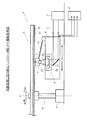
図1〜4は、本願発明に係る磁気ヘッドの参考例としての第1実施形態を示している。まず、図1を参照しながら、本願発明に係る磁気ヘッドが組み込まれた磁気情報処理装置の構成の一例について説明する。同図に示す磁気情報処理装置Pは、磁気ヘッドHと、キャリッジ6と、固定光学部7と、電源装置8とを備えた光磁気ディスク装置として構成されている。 1 to 4 show a first embodiment as a reference example of a magnetic head according to the present invention. First, an example of the configuration of a magnetic information processing apparatus incorporating a magnetic head according to the present invention will be described with reference to FIG. The magnetic information processing apparatus P shown in FIG. 1 is configured as a magneto-optical disk apparatus including a magnetic head H, a carriage 6, a fixed optical unit 7, and a power supply device 8.
光磁気ディスクDは、スピンドルSpに支持されており、スピンドルモータMの駆動力により、スピンドルSpを中心として高速回転可能である。光磁気ディスクDの両面のうち、磁気ヘッドHと対向する側の面には記録層40が設けられている。この記録層40の表面は、透光性を有する絶縁保護膜41によって覆われている。
The magneto-optical disk D is supported by the spindle Sp and can be rotated at high speed around the spindle Sp by the driving force of the spindle motor M. A
キャリッジ6は、光磁気ディスクDの下方に配されており、たとえば図示されていないボイスコイルモータの駆動力によって光磁気ディスクDの半径方向に移動自在である。このキャリッジ6の移動により、光磁気ヘッドHを目的のトラック近傍に配置させるシーク動作がなされる。固定光学部7は、レーザダイオードやコリメータレンズなど(いずれも図示略)を備えており、この固定光学部7から発せられたレーザ光Lは、キャリッジ6に向けて進行し、キャリッジ6に搭載された立ち上げミラー13に到達するように構成されている。固定光学部7には、ビームスプリッタや光検出器(いずれも図示略)も設けられている。
The carriage 6 is disposed below the magneto-optical disk D and is movable in the radial direction of the magneto-optical disk D by a driving force of a voice coil motor (not shown), for example. By the movement of the carriage 6, a seek operation for placing the magneto-optical head H in the vicinity of the target track is performed. The fixed optical unit 7 includes a laser diode, a collimator lens, and the like (both not shown), and the laser light L emitted from the fixed optical unit 7 travels toward the carriage 6 and is mounted on the carriage 6. It is configured to reach the rising
アクチュエータ9は、光磁気ディスクDへの記録および再生時における、フォーカス制御およびトラッキング制御を行なうためのものである。このアクチュエータ9は、キャリ
ッジ6に搭載されており、対物レンズ5bが搭載されたレンズホルダ10の上下方向および光磁気ディスクDの半径方向への移動を可能とするものである。
The
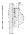
図2によく表われているように、磁気ヘッドHは、透明基板1と、この透明基板1に接合された対物レンズ5aと、薄膜コイル2と、磁性体膜3とを備えた光磁気ヘッドとして構成されている。透明基板1は、上下方向に撓み変形可能なサスペンション12に支持されており、光磁気ディスクDに対向して配されている。透明基板1は、これと光磁気ディスクDとの間に流入してくる空気流によりもたらされる、いわゆるくさび効果により、光磁気ディスクDとの間に微小な隙間を隔てて浮上するものである。このような透明基板1は、たとえば対物レンズ5aと同材質のガラス製であり、その表面には透光性を有する誘電体層4が形成されている。
As clearly shown in FIG. 2, the magnetic head H includes a
対物レンズ5aは、対物レンズ5bを透過してきたレーザ光Lを集束させ、光磁気ディスクDの記録層40の記録対象部分(磁区)にレーザスポットを形成するためのものである。
The
薄膜コイル2は、誘電体層4の内部において層をなすように形成されており、第1スパイラルコイル21と、第2スパイラルコイル22とを具備して構成されている。第1および第2スパイラルコイル21,22は、誘電体層4により互いに絶縁した状態で巻き方向が同一方向となるように、いわゆるバイファイラ巻き状に形成されている(図3参照)。これら第1および第2スパイラルコイル21,22は、対物レンズ5aや透明基板1を透過してきたレーザ光Lを遮らないように配置されており、対物レンズ5aの光軸Aがコイル中心部2aを通るようになっている。このような第1および第2スパイラルコイル21,22は、巻き数や長さ寸法などが同一となるように形成されており、そのため、これらのインダクタンスが同一になっている。磁性体膜3は、薄膜コイル2の下方に配されており、薄膜コイル2により発生した記録用磁界の下方への漏洩を抑制し、光磁気ディスクDに対して磁界を効率よく作用させるためのものである。この磁性体膜3は、パーマロイなどの高透磁率を有する物質からなり、レーザ光Lを遮らないように光軸Aがその中心部を通るように形成されている。
The
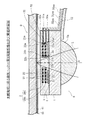
上記薄膜コイル2における第1および第2スパイラルコイル21,22のそれぞれは、外周端部21a,22aおよび内周端部21b,22bを有している。第1スパイラルコイル21の外周端部21aと第2スパイラルコイル22の外周端部22aとは、誘電体層4を介して互いに絶縁した状態にあり、これらの外周端部21a,22aは、薄膜コイル2の半径方向に延びる引き出し配線部31a,32aに個別に接続されている。引き出し配線部31a,32aのそれぞれは、透明基板1の外方へと延びる配線部材31aa,32aaに接続されており、これらの配線部材31aa,32aaは、図外のコイル駆動回路に通じている。一方、第1スパイラルコイル21の内周端部21bと第2スパイラルコイル22の内周端部22bとは、導体からなる結合部30を介して互いに結合した状態で一体となり、この結合部30は、薄膜コイル2の半径方向に延びる引き出し配線部30aに接続されている。結合部30に接続された引き出し配線部30aは、透明基板1の外方へと延びる配線部材30aaに接続されており、この配線部材30aaは、図外のコイル駆動回路に通じている。なお、結合部30に接続された引き出し配線部30aは、磁性体膜3とは分離して形成されたものあるいは磁性体膜3と一体に形成されたもののいずれであってもよいが、その余の引き出し配線部31a,32aは、磁性体膜3とは必ず分離して形成されている。
Each of the first and second spiral coils 21 and 22 in the
図3に模式的に示されているように、第1スパイラルコイル21の内周端部21bと第2スパイラルコイル22の内周端部22bとは、結合部30や引き出し配線部30aなどを介して基準電位0Vのグランド端子に共通接続されている。一方、第1スパイラルコイ
ル21の外周端部21aには、上記基準電位0Vとの電位差が正となるように、図外のコイル駆動回路から引き出し配線部31aなどを通じて+Vの電圧が印加される。また、第2スパイラルコイル22の外周端部22aには、上記基準電位0Vとの電位差が負となって上記+Vの電圧とは絶対値が同等の電圧となるように、図外のコイル駆動回路から引き出し配線部32aなどを通じて−Vの電圧が印加される。これにより、本実施形態の例によれば、第1スパイラルコイル21は、その外周端部21aに+Vの電圧が印加されて通電状態になると、コイル中心部2aからディスクD側へと進む上向きとなる磁束方向の記録用磁界を発生する。一方、第2スパイラルコイル22は、その外周端部22aに−Vの電圧が印加されて通電状態になると、上記第1スパイラルコイル21による上向きの磁束方向とは逆に、コイル中心部2aから透明基板1側へと進む下向きとなる磁束方向の記録用磁界を発生する。なお、第1スパイラルコイル21の外周端部21aには、−Vの電圧を印加する一方、第2スパイラルコイル22の外周端部22aには、+Vの電圧を印加するようにしてもよい。その場合、第1および第2スパイラルコイル21,22のそれぞれにおいて発生する記録用磁界の磁束方向は、上記とは逆向きとなる。
As schematically shown in FIG. 3, the inner
上記薄膜コイル2を駆動するためのコイル駆動回路は、図4に一例として示されるような構成となっている。図4に示されているように、コイル駆動回路においては、第1スパイラルコイル21の外周端部21aがスイッチングトランジスタS1を介して+Vの電源入力端子50に接続されているとともに、第2スパイラルコイル22の外周端部22aがスイッチングトランジスタS2を介して−Vの電源入力端子51に接続されている。第1および第2スパイラルコイル21,22の内周端部21b,22bは、電気抵抗素子55を介して基準電位0Vのグランド端子56に共通接続されている。スイッチングトランジスタS1には、入出力が同相となる増幅素子52を経て記録用データに対応するデジタル信号が入力され、このデジタル信号のH/Lに応じてスイッチングトランジスタS1がオン/オフされる。一方、スイッチングトランジスタS2には、入出力が逆相となる反転増幅素子53を経て上記記録用データに対応するデジタル信号が入力され、このデジタル信号のL/Hに応じてスイッチングトランジスタS2がオン/オフされるようになっている。つまり、コイル駆動回路は、記録用データに対応するデジタル信号に基づいて、第1および第2スパイラルコイル21,22の通電状態を排他的かつ高速に切り換えるように構成されている。
The coil drive circuit for driving the
このような薄膜コイル2を構成する第1および第2スパイラルコイル21,22、結合部30、引き出し配線部30a〜32a、および磁性体膜3などは、半導体製造プロセスと同様なプロセスにより製造することが可能である。第1および第2スパイラルコイル21,22、結合部30、引き出し配線部30a〜32aは、銅などの金属膜を所定形状にパターニングすることにより形成されたものであり、第1および第2スパイラルコイル21,22を覆うように誘電体の薄い層が形成される。同様に磁性体膜3も、パーマロイなどの膜をパターニングすることにより形成され、磁性体膜3を覆うように誘電体の薄い層が形成される。このような工程が繰り返されることにより、透明基板1の表面には、積層構造の誘電体層4が形成され、その内部に第1および第2スパイラルコイル21,22、結合部30、引き出し配線部30a〜32a、および磁性体膜3などが埋設された構造が得られる。
The first and second spiral coils 21 and 22, the
次に、磁気ヘッドHの作用について説明する。 Next, the operation of the magnetic head H will be described.
ディスクDへのデータの記録を磁界変調方式によって行う場合、このディスクDを回転させることにより、透明基板1をディスクDから微小な間隔を隔てて浮上させる。そして、記録層40の記録対象部分にレーザ光Lを連続的もしくは一定周波数で断続的に照射することにより、記録層40の温度を上昇させる。一方、薄膜コイル2により発生する記録用磁界は、第1スパイラルコイル21と第2スパイラルコイル22とで磁束方向が逆向き
とされ、これら第1および第2スパイラルコイル21,22がコイル駆動回路によって排他的に切り換えられながら駆動することにより、記録データの内容に応じて磁束方向が高速に反転させられる。これにより、記録層40を構成する磁性体の磁化の向きが制御され、その磁化の向きに応じた磁区が記録層40に形成されることでデータが記録される。
When recording data on the disk D by the magnetic field modulation method, the
このとき、第1スパイラルコイル21により発生する記録用磁界と第2スパイラルコイル22により発生する記録用磁界とのディスクDに対するそれぞれの強さは、磁束方向が高速反転しても同一レベルとされる。これは、第1および第2スパイラルコイル21,22のディスクDからの距離、巻き数、長さ寸法などといった物理的構成が同一であり、しかも、第1および第2スパイラルコイル21,22に対しては、正負が異なるものの同一レベルの電圧が印加されるためである。これにより、磁気ヘッドHは、薄膜コイル2の物理的構成やコイル駆動回路の電気的構成を単純な構成とした上で、ディスクDに対して磁束方向を高速に反転しつつも記録用磁界を安定して発生させることができる。
At this time, the strengths of the recording magnetic field generated by the
また、コイル駆動回路は、記録データに応じたデジタル信号に基づいて、第1および第2スパイラルコイル21,22の通電状態を排他的に切り換えるだけでよく、第1および第2スパイラルコイル21,22は、これらの一方が通電状態であれば他方が非通電状態となる。そのため、コイル駆動回路は、比較的周波数の高い高周波信号によることなく薄膜コイル2を適切に駆動することができ、これによりコイル駆動回路の省電力化を図ることができる。
Further, the coil drive circuit only needs to switch the energization state of the first and second spiral coils 21 and 22 exclusively based on the digital signal corresponding to the recording data, and the first and second spiral coils 21 and 22 can be switched. If one of these is energized, the other is de-energized. For this reason, the coil drive circuit can appropriately drive the
図5および図6は、本願発明に係る磁気ヘッドの参考例としての第2実施形態を示している。これらの図において、上記第1実施形態と同一または類似の要素には、上記第1実施形態と同一符号を付し、その説明を省略する。 5 and 6 show a second embodiment as a reference example of the magnetic head according to the present invention. In these drawings, the same or similar elements as those in the first embodiment are denoted by the same reference numerals as those in the first embodiment, and the description thereof is omitted.
図5および図6に示されているように、第2実施形態の磁気ヘッドHは、第1実施形態によるものとは薄膜コイル2の配線形態のみが異なる構成となっている。つまり、第1スパイラルコイル21の外周端部21aと第2スパイラルコイル22の外周端部22aとは、導体からなる引き出し配線部30aの基端に互いに結合した状態で一体となり、引き出し配線部30aの先端は、薄膜コイル2の半径方向に延びて配線部材30aaに接続されている。一方、第1スパイラルコイル21の内周端部21bと第2スパイラルコイル22の内周端部22bとは、誘電体層4を介して互いに絶縁した状態にあり、これらの内周端部21b,22bは、薄膜コイル2の半径方向に延びる引き出し配線部31a,32aに個別に接続されている。引き出し配線部31a,32aのそれぞれは、配線部材31aa,32aaに接続されている。これらの配線部材30aa〜32aaは、図外のコイル駆動回路に通じている。なお、内周端部21b,22bのそれぞれに接続された引き出し配線部31a,32aは、磁性体膜3とは分離して形成されており、その余の引き出し配線部30aについても、磁性体膜3とは必ず分離して形成されている。
As shown in FIGS. 5 and 6, the magnetic head H of the second embodiment has a configuration different from that of the first embodiment only in the wiring configuration of the
図6に模式的に示されているように、第1スパイラルコイル21の外周端部21aと第2スパイラルコイル22の内周端部22aとは、共に引き出し配線部30aを介して基準電位0Vのグランド端子に共通接続されている。一方、第1スパイラルコイル21の内周端部21bには、上記基準電位0Vとの電位差が正となるように、図外のコイル駆動回路から引き出し配線部31aなどを通じて+Vの電圧が印加される。また、第2スパイラルコイル22の内周端部22bには、上記基準電位0Vとの電位差が負となって上記+Vの電圧とは絶対値が同等の電圧となるように、図外のコイル駆動回路から引き出し配線部32aなどを通じて−Vの電圧が印加される。これにより、本実施形態の例によれば、第1スパイラルコイル21は、その内周端部21bに+Vの電圧が印加されて通電状態になると、コイル中心部2aから透明基板1側へと進む下向きとなる磁束方向の記録用磁界が発生する。一方、第2スパイラルコイル22は、その内周端部22bに−Vの電圧が印加さ
れて通電状態になると、上記第1スパイラルコイル21による下向きの磁束方向とは逆に、コイル中心部2aからディスクD側へと進む上向きとなる磁束方向の記録用磁界が発生する。なお、第1スパイラルコイル21の内周端部21bには、−Vの電圧を印加する一方、第2スパイラルコイル22の内周端部22bには、+Vの電圧を印加するようにしてもよい。その場合、第1および第2スパイラルコイル21,22のそれぞれにおいて発生する記録用磁界の磁束方向は、上記とは逆向きとなる。
As schematically shown in FIG. 6, the outer
上記薄膜コイル2を駆動するためのコイル駆動回路は、図4に一例として示されるような第1実施形態によるものと同様の構成となる。つまり、第2実施形態に対応するコイル駆動回路では、図4において第1および第2スパイラルコイル21,22の外周端部21a,22aと内周端部21b,22bとが入れ替わったものとなり、第1および第2スパイラルコイル21,22における磁束方向も逆向きになるだけである。
The coil drive circuit for driving the
したがって、第2実施形態の磁気ヘッドHによっても、薄膜コイル2の物理的構成やコイル駆動回路の電気的構成を単純な構成とした上で、ディスクDに対して磁束方向を高速に反転しつつも記録用磁界を安定して発生させることができる。また、コイル駆動回路は、比較的周波数の高い高周波信号によることなく薄膜コイル2を適切に駆動することができ、これによりコイル駆動回路の省電力化を図ることができる。
Therefore, even with the magnetic head H of the second embodiment, the physical configuration of the
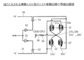
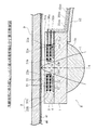
図7〜9は、本願発明に係る磁気ヘッドの一例としての第3実施形態を示している。これらの図においても、上記第1実施形態と同一または類似の要素には、上記第1実施形態と同一符号を付し、その説明を省略する。 7 to 9 show a third embodiment as an example of a magnetic head according to the present invention. Also in these drawings, the same or similar elements as those in the first embodiment are denoted by the same reference numerals as those in the first embodiment, and description thereof is omitted.
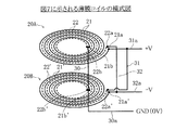
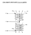
図7および図8に示されているように、第3実施形態の磁気ヘッドHにおいては、薄膜コイル2は、誘電体層4の内部において第1層20Aおよび第2層20Bの2層構造をなすように形成されている。第1層20Aは、ディスクDに近い層をなしており、この第1層20Aには、第1および第2スパイラルコイル21,22が互いに絶縁した状態で巻き方向が同一方向となるように、いわゆるバイファイラ巻き状に形成されている(図8参照)。第2層20Bは、第1層20Aと磁性体膜3との間に位置する層をなしており、この第2層20Bにおいても、第1および第2スパイラルコイル21’,22’が互いに絶縁した状態で巻き方向が同一方向となるように、いわゆるバイファイラ巻き状に形成されている(図8参照)。これら第1および第2スパイラルコイル21,21’,22,22’は、巻き数や長さ寸法、さらにコイルの巻き方向が全て同一となるように形成されている。
7 and 8, in the magnetic head H of the third embodiment, the
第1層20Aにおける第1スパイラルコイル21の外周端部21aと第2層20Bにおける第2スパイラルコイル22’の外周端部22a’とは、導体からなる結合部31を介して相互接続されており、これにより第1層20Aと第2層20Bとの間で連結対となった外周端部21a,22a’は、薄膜コイル2の半径方向に延びる引き出し配線部31aに共通接続されている。この引き出し配線部31aは、透明基板1の外方へと延びる配線部材31aaに接続されており、この配線部材31aaは、図外のコイル駆動回路に通じている。また、第1層20Aにおける第2スパイラルコイル22の外周端部22aと第2層20Bにおける第1スパイラルコイル21’の外周端部21a’についても、導体からなる結合部32を介して相互接続されており、こうして第1層20Aと第2層20Bとの間で連結対となった外周端部22a,21a’は、薄膜コイル2の半径方向に延びる引き出し配線部32aに共通接続されている。この引き出し配線部32aは、透明基板1の外方へと延びる配線部材32aaに接続されており、この配線部材32aaも、図外のコイル駆動回路に通じている。一方、第1層20Aにおける第1および第2スパイラルコイル21,22の内周端部21b,22bと第2層20Bにおける第1および第2スパイラルコイル21’,22’の内周端部21b’,22b’とは、導体からなる結合部30に一
括接続されており、この結合部30は、薄膜コイル2の半径方向に延びる引き出し配線部30aに接続されている。結合部30に接続された引き出し配線部30aは、透明基板1の外方へと延びる配線部材30aaに接続されており、この配線部材30aaは、図外のコイル駆動回路に通じている。なお、結合部30に接続された引き出し配線部30aは、磁性体膜3とは同一層ではあるが分離して形成されたもの、あるいは磁性体膜3と同一層で一体に形成されたもののいずれであってもよいが、その余の引き出し配線部31a,32aは、磁性体膜3とは必ず分離して形成されている。
The outer
図8に模式的に示されているように、第1層20Aおよび第2層20Bにおける全ての内周端部21b,22b,21b’,22b’は、結合部30や引き出し配線部30aなどを介して基準電位0Vのグランド端子に共通接続されている。一方、第1層20Aおよび第2層20Bにおけるスパイラルコイル21,22’の外周端部21a,22a’には、上記基準電位0Vとの電位差が正となるように、図外のコイル駆動回路から引き出し配線部31aなどを通じて+Vの電圧が印加される。また、第1層20Aおよび第2層20Bにおけるスパイラルコイル22,21’の外周端部22a,21a’には、上記基準電位0Vとの電位差が負となって上記+Vの電圧とは絶対値が同等の電圧となるように、図外のコイル駆動回路から引き出し配線部32aなどを通じて−Vの電圧が印加される。つまり、第1層20Aおよび第2層20Bにおけるスパイラルコイル21,22’は、電気的に並列接続された関係にある。また、第1層20Aおよび第2層20Bにおけるスパイラルコイル22,21’も、電気的に並列接続された関係にあり、これらスパイラルコイル21,22’の対からなる回路とスパイラルコイル22,21’の対からなる回路とは、電気的に切り離された状態にある。これにより、本実施形態の例によれば、第1層20Aおよび第2層20Bにわたるスパイラルコイル21,22’は、これらの外周端部21a,22a’に+Vの電圧が印加されて通電状態になると、たとえばコイル中心部2aから透明基板1側へと進む下向きとなる磁束方向の記録用磁界を同時に発生する。一方、第1層20Aおよび第2層20Bにわたる第2スパイラルコイル22,21’は、これらの外周端部22a,21a’に−Vの電圧が印加されて通電状態になると、上記スパイラルコイル21,22’による下向きの磁束方向とは逆に、コイル中心部2aからディスクD側へと進む上向きとなる磁束方向の記録用磁界を同時に発生する。なお、スパイラルコイル21,22’の外周端部21a,22a’には、−Vの電圧を印加する一方、スパイラルコイル22,21’の外周端部22a,21a’には、+Vの電圧を印加するようにしてもよい。その場合、スパイラルコイル21,22’において同時発生する記録用磁界とスパイラルコイル22,21’において同時発生する記録用磁界との磁束方向は、上記とは逆向きとなる。
As schematically shown in FIG. 8, all inner
上記薄膜コイル2を駆動するためのコイル駆動回路は、図9に一例として示されるような構成となっている。図9に示されているように、コイル駆動回路においては、スパイラルコイル21,22’の外周端部21a,22a’がスイッチングトランジスタS1を介して+Vの電源入力端子50に共通接続されているとともに、スパイラルコイル22,21’の外周端部22a,21a’がスイッチングトランジスタS2を介して−Vの電源入力端子51に共通接続されている。全ての内周端部21b,22b,21b’,22b’は、電気抵抗素子55を介して基準電位0Vのグランド端子56に共通接続されている。スイッチングトランジスタS1には、入出力が同相となる増幅素子52を経て記録用データに対応するデジタル信号が入力され、このデジタル信号のH/Lに応じてスイッチングトランジスタS1がオン/オフされる。一方、スイッチングトランジスタS2には、入出力が逆相となる反転増幅素子53を経て上記記録用データに対応するデジタル信号が入力され、このデジタル信号のL/Hに応じてスイッチングトランジスタS2がオン/オフされるようになっている。つまり、コイル駆動回路は、記録用データに対応するデジタル信号に基づいて、スパイラルコイル21,22’の通電状態とスパイラルコイル22,21’の通電状態とを排他的かつ高速に切り換えるように構成されている。
A coil drive circuit for driving the
このようなコイル駆動回路によって薄膜コイル2が駆動されるとき、スパイラルコイル21,22’により同一磁束方向で同時発生する記録用磁界の強さと、スパイラルコイル22,21’により同一磁束方向で同時発生する記録用磁界の強さとは、磁束方向が互いに逆方向であっても同一レベルとされる。これは、全てのスパイラルコイル21,21’,22,22’の巻き数や長さ寸法などが同一であり、しかも、スパイラルコイル21,22’の組とスパイラルコイル22,21’の組に対しては、各組ごとに正負が異なるものの同一レベルの電圧が印加されるためである。また、第1層20Aおよび第2層20Bから同時に記録用磁界が発生するためでもある。したがって、第3実施形態の磁気ヘッドHによれば、薄膜コイル2の物理的構成やコイル駆動回路の電気的構成を単純な構成とした上で、ディスクDに対して磁束方向を高速に反転しつつもより強い記録用磁界を安定して発生させることができる。
When the
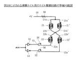
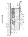
図10〜12は、本願発明に係る磁気ヘッドの参考例としての第4実施形態を示している。これらの図においては、上記第1および第3実施形態と同一または類似の要素には、上記第1および第3実施形態と同一符号を付し、その説明を省略する。 10 to 12 show a fourth embodiment as a reference example of the magnetic head according to the present invention. In these drawings, the same or similar elements as those in the first and third embodiments are denoted by the same reference numerals as those in the first and third embodiments, and the description thereof is omitted.
図10および図11に示されているように、第4実施形態の磁気ヘッドHにおいては、第1層20Aにおける第1スパイラルコイル21の外周端部21aと第2層20Bにおける第1スパイラルコイル21’の外周端部21a’とは、導体からなる結合部33を介して相互接続されており、この相互接続により第1層20Aと第2層20Bとの間で連結対となった外周端部21a,21a’は、薄膜コイル2の半径方向に延びる引き出し配線部30aに接続されている。第1層20Aにおける第2スパイラルコイル22の外周端部22aは、薄膜コイル2の半径方向に延びる引き出し配線部31aに直接的に接続されている。また、第2層20Bにおける第2スパイラルコイル22’の外周端部22a’も、薄膜コイル2の半径方向に延びる引き出し配線部32aに直接的に接続されている。一方、第1層20Aにおける第1スパイラルコイル21の内周端部21bは、結合部34を介して第2層20Bにおける第2スパイラルコイル22’の内周端部22b’に相互接続されており、この結合部34には、引き出し配線部が接続されていない。また、第1層20Aにおける第2スパイラルコイル22の内周端部22bは、結合部35を介して第2層20Bにおける第1スパイラルコイル21’の内周端部21b’に相互接続されており、この結合部35についても、引き出し配線部が接続されていない。なお、図11に示されているように、第1層20Aのコイルの巻き方向と第2層20Bのコイルの巻き方向とは、互いに逆方向となっている。
As shown in FIGS. 10 and 11, in the magnetic head H of the fourth embodiment, the outer
図11に模式的に示されているように、第1層20Aおよび第2層20Bにおける第1スパイラルコイル21,21’の外周端部21a,21a’は、基準電位0Vに対して電位差が+Vとなる正極端子に共通接続されている。一方、第1層20Aにおける第2スパイラルコイル22の外周端部22aには、引き出し配線部31aなどを介して基準電位0Vの電位が印加されるようになっている。また、第2層20Bにおける第2スパイラルコイル22’の外周端部22a’も、引き出し配線部32aなどを介して基準電位0Vの電位が印加されるようになっている。つまり、第1層20Aの第2スパイラルコイル22と第2層20Bの第1スパイラルコイル21’とは、互いに結合部35を介して電気的に直列接続された関係にある。また、第2層20Bの第2スパイラルコイル22’と第1層20Aの第1スパイラルコイル21とは、互いに結合部34を介して電気的に直列接続された関係にある。これら第2スパイラルコイル22および第1スパイラルコイル21’の対からなる回路と第2スパイラルコイル22’および第1スパイラルコイル21の対からなる回路とは、電気的に切り離された状態にある。これにより、本実施形態の例によれば、第1層20Aにおける第2スパイラルコイル22の外周端部22aがグランド接続された状態になると、第1層20Aの第2スパイラルコイル22および第2層20Bの第1スパ
イラルコイル21’は、たとえばコイル中心部2aからディスクD側へと進む上向きとなる磁束方向の記録用磁界を同時に発生する。一方、第2層20Bにおける第2スパイラルコイル22’の外周端部22a’がグランド接続された状態になると、第1層20Aの第1スパイラルコイル21および第2層20Bの第2スパイラルコイル22’は、上記上向きの磁束方向とは逆に、コイル中心部2aから透明基板1側へと進む下向きとなる磁束方向の記録用磁界を同時に発生する。
As schematically shown in FIG. 11, the outer peripheral ends 21a and 21a ′ of the first spiral coils 21 and 21 ′ in the
上記薄膜コイル2を駆動するためのコイル駆動回路は、図12に一例として示されるような構成となっている。図12に示されているように、コイル駆動回路においては、第1層20Aにおける第2スパイラルコイル22の外周端部22aがスイッチングトランジスタS1を介してグランド端子56に接続されているとともに、第2層20Bにおける第2スパイラルコイル22’の外周端部22a’がスイッチングトランジスタS2を介してグランド端子56に接続されている。第1層20Aおよび第2層20Bにおける第1スパイラルコイル21,21’の外周端部21a,21a’は、電気抵抗素子55を介して+Vの電源入力端子50に共通接続されている。また、第1層20Aにおける第1スパイラルコイル21の内周端部21bは、第2層20Bにおける第2スパイラルコイル22’の内周端部22b’に直接連結されており、第1層20Aにおける第2スパイラルコイル22の内周端部22bは、第2層20Bにおける第1スパイラルコイル21’の内周端部21b’に直接連結されている。スイッチングトランジスタS1には、入出力が同相となる増幅素子52を経て記録用データに対応するデジタル信号が入力され、このデジタル信号のH/Lに応じてスイッチングトランジスタS1がオン/オフされる。一方、スイッチングトランジスタS2には、入出力が逆相となる反転増幅素子53を経て上記記録用データに対応するデジタル信号が入力され、このデジタル信号のL/Hに応じてスイッチングトランジスタS2がオン/オフされるようになっている。つまり、コイル駆動回路は、記録用データに対応するデジタル信号に基づいて、第1スパイラルコイル21および第2スパイラルコイル22’の通電状態と第2スパイラルコイル22および第1スパイラルコイル21’の通電状態とを排他的かつ高速に切り換えるように構成されている。
A coil driving circuit for driving the
このようなコイル駆動回路によって薄膜コイル2が駆動されるとき、第1スパイラルコイル21および第2スパイラルコイル22’の組により同一磁束方向で同時発生する記録用磁界の強さと、第2スパイラルコイル22および第1スパイラルコイル21’の組により同一磁束方向で同時発生する記録用磁界の強さとは、磁束方向が互いに逆方向であっても同一レベルとされる。これは、全てのスパイラルコイル21,21’,22,22’の巻き数や長さ寸法などが同一であり、しかも、第1スパイラルコイル21および第2スパイラルコイル22’の組と第2スパイラルコイル22および第1スパイラルコイル21’の組に対しては、各組ごとに正負が異なるものの同一レベルの電圧が印加されるためである。また、第1層20Aおよび第2層20Bから同時に記録用磁界が発生するためでもある。したがって、第4実施形態の磁気ヘッドHによっても、薄膜コイル2の物理的構成やコイル駆動回路の電気的構成を単純な構成とした上で、ディスクDに対して磁束方向を高速に反転しつつもより強い記録用磁界を安定して発生させることができる。
When the
1 透明基板
21 第1スパイラルコイル
21a 外周端部
21b 内周端部
22 第2スパイラルコイル
22a 外周端部
22b 内周端部
30a 引き出し配線部
31a 引き出し配線部
32a 引き出し配線部
DESCRIPTION OF
Claims (3)
上記第1層における第1および第2スパイラルコイルの巻き方向と上記第2層における第1および第2スパイラルコイルの巻き方向とは、互いに同一となる方向であり、
上記第1層における第1および第2スパイラルコイルのいずれか一方の外周端部は、上記第2層における第1および第2スパイラルコイルのいずれか一方の外周端部に相互接続されているとともに、上記第1層および第2層におけるその余のスパイラルコイルの外周端部もまた上記相互接続とは別に相互接続されており、各相互接続により連結対となった上記第1層および第2層のスパイラルコイルの外周端部は、連結対ごとに上記基板の側部へと引き延ばされており、かつ、
上記第1層における第1および第2スパイラルコイルの内周端部は、互いに結合した状態で上記第2層における第1および第2スパイラルコイルの内周端部に一括接続されているとともに、一括接続により一体となった上記第1層および第2層のスパイラルコイルの内周端部は、上記第1層および第2層とは異なる層を経て上記基板の側部へと引き延ばされていることを特徴とする、薄膜コイル。 Each of the first layer and the second layer on the substrate is provided with first and second spiral coils formed in a bifilar winding, and each of the first and second spiral coils in each of the layers includes an outer peripheral end portion and an inner end portion. A thin film coil having a peripheral end,
The winding direction of the first and second spiral coils in the first layer and the winding direction of the first and second spiral coils in the second layer are the same direction.
The outer peripheral end of one of the first and second spiral coils in the first layer is interconnected to the outer peripheral end of either the first or second spiral coil in the second layer, and The outer peripheral ends of the remaining spiral coils in the first layer and the second layer are also interconnected separately from the interconnections, and the first layer and the second layer that are connected to each other by the interconnections are connected to each other. The outer peripheral end of the spiral coil is extended to the side of the substrate for each connection pair, and
The inner peripheral ends of the first and second spiral coils in the first layer are collectively connected to the inner peripheral ends of the first and second spiral coils in the second layer in a state of being coupled to each other. The inner peripheral end portions of the spiral coils of the first layer and the second layer integrated by the connection are extended to the side portion of the substrate through a layer different from the first layer and the second layer. A thin film coil, characterized in that
上記第1層における第1および第2スパイラルコイルの内周端部と上記第2層における第1および第2スパイラルコイルの内周端部とを常に所定の基準電位とし、かつ、 The inner peripheral ends of the first and second spiral coils in the first layer and the inner peripheral ends of the first and second spiral coils in the second layer are always set to a predetermined reference potential, and
上記第1層および第2層におけるスパイラルコイルの外周端部で相互接続により連結対となったもののうち、いずれか一方の連結対を上記基準電位との電位差が正となる通電状態とするのに対し、他方の連結対を上記基準電位との電位差が負となる通電状態とし、これらの通電状態を排他的に切り換え可能に構成されていることを特徴とする、コイル駆動回路。 Of the first and second layers of the spiral coils, the outer peripheral ends of the spiral coils are connected to each other by being connected to each other so that one of the connected pairs is in an energized state in which the potential difference from the reference potential is positive. On the other hand, a coil drive circuit characterized in that the other connected pair is in an energized state in which the potential difference from the reference potential is negative, and these energized states can be switched exclusively.
Priority Applications (2)
| Application Number | Priority Date | Filing Date | Title |
|---|---|---|---|
| JP2004272190A JP4331663B2 (en) | 2004-09-17 | 2004-09-17 | Thin film coil, coil drive circuit, and magnetic head |
| US11/006,994 US7324411B2 (en) | 2004-09-17 | 2004-12-08 | Thin-film coil, coil driving circuit and magnetic head |
Applications Claiming Priority (1)
| Application Number | Priority Date | Filing Date | Title |
|---|---|---|---|
| JP2004272190A JP4331663B2 (en) | 2004-09-17 | 2004-09-17 | Thin film coil, coil drive circuit, and magnetic head |
Publications (2)
| Publication Number | Publication Date |
|---|---|
| JP2006085873A JP2006085873A (en) | 2006-03-30 |
| JP4331663B2 true JP4331663B2 (en) | 2009-09-16 |
Family
ID=36125364
Family Applications (1)
| Application Number | Title | Priority Date | Filing Date |
|---|---|---|---|
| JP2004272190A Expired - Fee Related JP4331663B2 (en) | 2004-09-17 | 2004-09-17 | Thin film coil, coil drive circuit, and magnetic head |
Country Status (2)
| Country | Link |
|---|---|
| US (1) | US7324411B2 (en) |
| JP (1) | JP4331663B2 (en) |
Families Citing this family (1)
| Publication number | Priority date | Publication date | Assignee | Title |
|---|---|---|---|---|
| US7486167B2 (en) * | 2005-08-24 | 2009-02-03 | Avago Technologies General Ip (Singapore) Pte. Ltd. | Cross-coupled inductor pair formed in an integrated circuit |
Family Cites Families (9)
| Publication number | Priority date | Publication date | Assignee | Title |
|---|---|---|---|---|
| JPH11259813A (en) | 1998-03-11 | 1999-09-24 | Sony Corp | Thin film coil, magnetic head and magneto-optical head |
| JP2001185419A (en) | 1999-12-22 | 2001-07-06 | Sanyo Electric Co Ltd | Thin film coil element and manufacturing method for same |
| JP3362034B2 (en) * | 2001-01-16 | 2003-01-07 | ティーディーケイ株式会社 | Thin film magnetic head and method of manufacturing the same |
| US6654203B2 (en) * | 2001-04-25 | 2003-11-25 | Tdk Corporation | Thin-film magnetic head and method of manufacturing same, head gimbal assembly and hard disk drive |
| JP2003051144A (en) | 2001-08-03 | 2003-02-21 | Fujitsu Ltd | Magnetic head |
| JP3668189B2 (en) * | 2001-12-27 | 2005-07-06 | 富士通株式会社 | Optical head and optical information processing apparatus |
| JP2003282324A (en) | 2002-03-22 | 2003-10-03 | Tdk Corp | Microdevice and its manufacturing method |
| JP3790224B2 (en) | 2003-03-12 | 2006-06-28 | 富士通株式会社 | Magnetic head |
| JP2005141810A (en) * | 2003-11-05 | 2005-06-02 | Fujitsu Ltd | Magneto-optical head and magneto-optical disk apparatus |
-
2004
- 2004-09-17 JP JP2004272190A patent/JP4331663B2/en not_active Expired - Fee Related
- 2004-12-08 US US11/006,994 patent/US7324411B2/en not_active Expired - Fee Related
Also Published As
| Publication number | Publication date |
|---|---|
| US7324411B2 (en) | 2008-01-29 |
| US20060072385A1 (en) | 2006-04-06 |
| JP2006085873A (en) | 2006-03-30 |
Similar Documents
| Publication | Publication Date | Title |
|---|---|---|
| JP4144867B2 (en) | Magnetic disk unit | |
| US8842505B2 (en) | Magnetic disk device and method of controlling magnetic head | |
| US6721110B2 (en) | Optical pickup actuator driving method and apparatus therefor | |
| KR950007300B1 (en) | External magnetic field generation apparatus | |
| US5278809A (en) | Photomagnetic recording apparatus recording with alternating magnetic field and D.C. magnetic field | |
| JP4331663B2 (en) | Thin film coil, coil drive circuit, and magnetic head | |
| KR100486246B1 (en) | Optical pick-up actuator and optical recording/reproducing apparatus | |
| JP2005006496A (en) | Ultra-small mold coil device for actuator, optical pickup actuator, optical pickup device and optical disk drive using the same | |
| JP2004295932A (en) | Objective lens driving device for optical head | |
| JP2001273659A (en) | Structure of conductor suspension type actuator and current path arrangement method | |
| JP3790224B2 (en) | Magnetic head | |
| US6760278B2 (en) | Magnetic head and data recording and reproduction device | |
| JP2002025011A (en) | Magnetic head and magnetic recording device | |
| CN101286325B (en) | Optical pickup and method for manufacturing the same | |
| JP3024662B2 (en) | Coil driving device and information recording device | |
| KR100493066B1 (en) | Very small molded coil device for actuator, and optical pickup apparatus and optical disc drive using the same | |
| JP2004110985A (en) | Actuator and optical pickup device | |
| JP2005353117A (en) | Magneto-optical recording device | |
| US20070121428A1 (en) | Information recording apparatus | |
| JP2940649B2 (en) | Magnetic field generator for magneto-optical recording | |
| CN100431024C (en) | Magneto-optical recording system | |
| JP2007299469A (en) | Optical pickup and optical disc apparatus | |
| KR100316230B1 (en) | Piezoelectric Actuator for optical Pick-up Device | |
| JP2000020979A (en) | Biaxial actuator, optical pickup and optical disk device incorporating the same | |
| JP3378190B2 (en) | Optical pickup actuator |
Legal Events
| Date | Code | Title | Description |
|---|---|---|---|
| A621 | Written request for application examination |
Free format text: JAPANESE INTERMEDIATE CODE: A621 Effective date: 20070824 |
|
| A977 | Report on retrieval |
Free format text: JAPANESE INTERMEDIATE CODE: A971007 Effective date: 20090408 |
|
| A131 | Notification of reasons for refusal |
Free format text: JAPANESE INTERMEDIATE CODE: A131 Effective date: 20090414 |
|
| A521 | Written amendment |
Free format text: JAPANESE INTERMEDIATE CODE: A523 Effective date: 20090518 |
|
| TRDD | Decision of grant or rejection written | ||
| A01 | Written decision to grant a patent or to grant a registration (utility model) |
Free format text: JAPANESE INTERMEDIATE CODE: A01 Effective date: 20090616 |
|
| A01 | Written decision to grant a patent or to grant a registration (utility model) |
Free format text: JAPANESE INTERMEDIATE CODE: A01 |
|
| A61 | First payment of annual fees (during grant procedure) |
Free format text: JAPANESE INTERMEDIATE CODE: A61 Effective date: 20090618 |
|
| R150 | Certificate of patent or registration of utility model |
Free format text: JAPANESE INTERMEDIATE CODE: R150 |
|
| FPAY | Renewal fee payment (event date is renewal date of database) |
Free format text: PAYMENT UNTIL: 20120626 Year of fee payment: 3 |
|
| FPAY | Renewal fee payment (event date is renewal date of database) |
Free format text: PAYMENT UNTIL: 20120626 Year of fee payment: 3 |
|
| FPAY | Renewal fee payment (event date is renewal date of database) |
Free format text: PAYMENT UNTIL: 20130626 Year of fee payment: 4 |
|
| FPAY | Renewal fee payment (event date is renewal date of database) |
Free format text: PAYMENT UNTIL: 20130626 Year of fee payment: 4 |
|
| LAPS | Cancellation because of no payment of annual fees |