JP4327266B2 - Pattern dimension evaluation method and pattern formation method - Google Patents
Pattern dimension evaluation method and pattern formation method Download PDFInfo
- Publication number
- JP4327266B2 JP4327266B2 JP04060398A JP4060398A JP4327266B2 JP 4327266 B2 JP4327266 B2 JP 4327266B2 JP 04060398 A JP04060398 A JP 04060398A JP 4060398 A JP4060398 A JP 4060398A JP 4327266 B2 JP4327266 B2 JP 4327266B2
- Authority
- JP
- Japan
- Prior art keywords
- pattern
- monitor
- diffracted light
- development
- order diffracted
- Prior art date
- Legal status (The legal status is an assumption and is not a legal conclusion. Google has not performed a legal analysis and makes no representation as to the accuracy of the status listed.)
- Expired - Fee Related
Links
Images


Classifications
-
- G—PHYSICS
- G01—MEASURING; TESTING
- G01N—INVESTIGATING OR ANALYSING MATERIALS BY DETERMINING THEIR CHEMICAL OR PHYSICAL PROPERTIES
- G01N21/00—Investigating or analysing materials by the use of optical means, i.e. using sub-millimetre waves, infrared, visible or ultraviolet light
- G01N21/84—Systems specially adapted for particular applications
- G01N21/88—Investigating the presence of flaws or contamination
- G01N21/95—Investigating the presence of flaws or contamination characterised by the material or shape of the object to be examined
- G01N21/956—Inspecting patterns on the surface of objects
Landscapes
- General Health & Medical Sciences (AREA)
- Physics & Mathematics (AREA)
- Life Sciences & Earth Sciences (AREA)
- Chemical & Material Sciences (AREA)
- Analytical Chemistry (AREA)
- Biochemistry (AREA)
- Health & Medical Sciences (AREA)
- General Physics & Mathematics (AREA)
- Immunology (AREA)
- Pathology (AREA)
- Length Measuring Devices By Optical Means (AREA)
- Exposure And Positioning Against Photoresist Photosensitive Materials (AREA)
- Exposure Of Semiconductors, Excluding Electron Or Ion Beam Exposure (AREA)
- Photosensitive Polymer And Photoresist Processing (AREA)
Description
【0001】
【発明の属する技術分野】
本発明は、半導体装置の作製における光リソグラフィのレジストパターン形成技術に係わり、特に現像中若しくは現像後のレジストパターンを評価するためのパターン寸法評価方法及びパターン形成方法に関するものである。
【0002】
【従来の技術】
ウエハ上に集積回路パターンを形成するには、ウエハ上にレジストを塗布した後に該レジストに所望のパターンを露光し、さらに現像処理してレジストパターンを形成し、これをマスクにエッチング等の加工を行う。マスクとしてのレジストパターンには高い寸法精度が要求されるが、レジストパターンの寸法は現像時間により大きく変わる。このため、現像時間の制御が非常に重要である。
【0003】
従来、現像時の寸法制御は、先行ウエハを露光し、現像した後、その寸法評価を行うことで最適現像時間を決め、全てのウエハの現像時間を一定として行ってきた。しかし、実際にはそれぞれのウエハの引き置き時間といったウエハ履歴が異なっているために、同一ロットを同一現像時間で現像を行うとウエハ間に寸法ばらつきが生じ、所望寸法で現像を終わらせることができない。
【0004】
これまではこのような現像の時間管理を行っていても、寸法誤差が許容範囲内に入っていたため大きな問題とはなっていなかったが、プロセスの微細化が進みこれまで以上に精密な寸法制御が必要となってきており、従来の現像時間管理手法では現像時の寸法制御が困難となっている。
【0005】
一方、従来では現像後に行うレジストパターンの評価は、例えばSEM(Scanning Electron Microscope)を用いて行ってきた。SEMは高倍率のパターン観察が可能である反面、装置構成が複雑でかつ高価である。また、検査に非常に長い時間を要するため、効率良く評価することが困難であった。
【0006】
また、現像中や現像後に限らず、回折光等を利用して光学的にデバイスパターンを検査する場合、必要なデバイスパターンのモニタの際に他のデバイスパターンからの情報も取り込まれる可能性があり、これがモニタの精度を劣化させる要因となっていた。
【0007】
【発明が解決しようとする課題】
このように従来、現像時間の制御により異なるウエハに対してレジストパターンの精密な寸法制御を行うことは困難であった。また、レジストパターンをSEMで評価するには多大な時間がかかるという問題があった。さらに、回折光等を利用してデバイスパターンを検査する場合、モニタすべきパターンとは別のパターンからの影響でモニタ精度が低下する問題があった。
【0008】
本発明は、上記の事情を考慮して成されたもので、その目的とするところは、異なるウエハに対してもレジストパターンの精密な寸法制御が可能となるパターン寸法評価方法及びパターン形成方法を提供することにある。
【0009】
本発明の他の目的は、モニタすべきパターンとは別のパターンからの影響を受けることなく、レジストパターンを短時間で高精度に検査することのできるパターン寸法評価方法及びパターン形成方法を提供することにある。
【0010】
本発明のさらなる他の目的は、レジストパターンの寸法を、その現像中に短時間でかつ高精度に評価でき、現像の終点を高精度に予測することのできるパターン寸法評価方法及びパターン形成方法を提供することにある。
【0011】
【課題を解決するための手段】
(構成)
上記課題を解決するための本発明の一態様であるパターン評価方法は、被処理基板上のレジスト膜を露光し、前記レジスト膜を現像することによってデバイスパターン及びモニタパターンを形成し、前記デバイスパターンの寸法を前記モニタパターンに照射した光の回折光強度に基づいて評価する、パターン寸法評価方法であって、デバイスマスクパターンとモニタマスクパターンとを具備するマスクを用いて1ショットで前記レジスト膜を露光し、前記デバイスマスクパターンと前記モニタマスクパターンを前記レジスト膜に転写するステップと、露光された前記レジスト膜を現像することによって、前記デバイスパターン及び前記モニタパターンを形成するステップと、前記現像中又は現像後に、所定の波長の平行光を前記モニタパターンに照射するステップと、前記モニタパターンからの回折光強度を検出するステップと、前記モニタパターンからの回折光強度に基づいて前記デバイスパターンの寸法を評価するステップとを具備し、前記モニタマスクパターンは、円形又は多角形のパターンが二次元的に周期的に配置され、且つパターン間隔が使用する露光装置の解像限界以下になるように配置されることにより、前記現像中又は現像後に前記モニタパターン及び前記デバイスパターンに所定の波長の光が照射された場合の、前記モニタパターンの現像に伴う回折光強度の変化が、前記デバイスパターンの現像による寸法変化に対する回折光強度の変化よりも大きくなるように形成されることを特徴とする。
【0019】
(作用)
本発明では、レジストの現像中又は現像後に、デバイスパターンや既加工パターンから識別可能な要素からなるモニタ領域を用いてパターン評価を行うことにより、レジストパターンの寸法を検査することができる。
【0020】
そしてモニタ領域にモニタパターンを露光により形成する場合、例えば露光マスクの要素パターンとして円形又は多角形を用い、しかもそのパターン間隔が使用する露光装置の解像限界以下になるように構成した露光マスクを使用して露光を行なう。このようにして形成されたモニタパターンによれば、現像時間の経過による回折光の強度変化をデバイスパターンよりも大きくすることができ、これにより検査精度の向上をはかることができる。
【0021】
また、ピッチ又は繰り返しの方向等が異なるモニタパターンを用いてパターン評価を行うことにより、他のパターンからの影響を受けない精度良い検査が可能となる。さらに、回折光強度をモニタするだけでパターン評価を行うことができるので、SEM等は異なり短時間で検査することができる。
【0022】
一方、モニタ領域として、前記のようなパターンを有さず、ただ全体に亘って略均一の現像速度となるように露光され、現像の進行に伴い略均一に膜減りが生じるように形成されているものを用いる場合、このモニタ領域からの回折光強度には極大・極小を観察することができる。そして、この極大、極小に基づいてデバイスパターンの現像終点を予測することができる。
【0023】
このような予測方法によれば、回折光強度信号の絶対値に信号的なオフセットが生じている場合であっても、極大、極小に基づいてデバイスパターンの現像終点を予測するようにしたので、このオフセットを補正して正確な現像終点を求めることが可能になる。
【0024】
【発明の実施の形態】
以下、本発明の詳細を図示の実施形態によって説明する。
【0025】
(第1の実施形態)
図1は、本発明の第1の実施形態に係わるパターン寸法評価装置を説明するためのもので、1次回折光を利用して現像後にパターン検査を行う装置構成例を示す図である。
【0026】
ウエハ(被処理基板)100上のレジスト110には、デバイスパターン111と共にモニタパターン112が、一括露光、現像処理により形成されている。モニタパターン112は、1ショット内においてデバイス作成に寄与するエリアと分離して配置されている。
【0027】
モニタパターン112に対し、光源201から、狭帯域フィルタを介して400±20nmとした波長の平行光を入射させる。モニタパターン112からは0次の回折光202、1次の回折光203、さらに高次の回折光(図示せず)が得られる。そして、モニタパターン112からの1次回折光203をCCDカメラ210によって検出する。このCCDカメラ210は、コンピュータシステムからなるパターン評価部220に接続されており、このパターン評価部220は、検出された1次回折光203の強度を予め得られている寸法と1次回折光強度との関係に適用し、デバイスパターン寸法の評価を行う。
【0028】
図2は、本実施形態における現像モニタパターン112の例を示す図である。1辺の長さL=0.2μm(ウエハ換算値、以下同様)の正方形が規則的に配置されており、隣接する4つの正方形の中心が四角形の頂点になるように配置されている。x方向の間隔dx、y方向の間隔dyは共に0.07μmである。ここで、間隔dx、dy=0.07μmは使用する露光装置の解像限界以下の値である。
【0029】
デバイスパターン111として0.15μmのL&Sパターンを想定した。露光条件は露光波長=248nm(KrFエキシマレーザ)、投影光学系の開口数(NA)=0.7、コヒーレンスファクタ(σ)=0.75、2/3輪帯照明とし、レジストには0.15μm膜厚のポジ型化学増幅レジストを用いた。
【0030】
そして、0.15μmのL&Sデバイスパターン(ライン幅:スペース幅=1:1)111が現像時間30秒で所望寸法に仕上がる条件で、モニターパターン112を以下の寸法として露光を行なった。すなわち、
(a)…図2に示したモニタパターン。
【0031】
(b)…0.15μmのL&Sモニタパターン(ライン幅:スペース幅=1:1)。
【0032】
(c)…0.15μmのL&Sモニタパターン(仕上がりのライン幅:スペース幅=1:3)。
【0033】
(d)…ライン幅0.07μm、スペース幅0.2μmのL&Sモニタパターン。
【0034】
ここで(b)は、前記デバイスパターン111と同一寸法であるため、この(b)との比較により、デバイスパターン111に対する1次回折光の強度変化を知ることができる。
【0035】
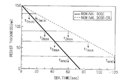
(a)〜(d)それぞれの現像時間(10〜36秒)に対する現像後の1次回折光強度の関係は、図3に示すようになる。このとき、(d)のパターンは全く解像していなかったため、図示されていない。
【0036】
現像終点近傍(30秒)で(b)のパターンでは殆ど強度変化がなく、(a)のモニタパターンは(c)のパターンの約4倍の強度変化を示した。このとき、(a)のモニタパターンの強度変化は、(b)の0.15μmのL&Sパターン(ライン幅:スペース幅=1:1)の寸法1.5nmの変化に対して、10(CCDカメラの階調を256とした場合)である。
【0037】
この原因として、以下のようなことがあげられる。
【0038】
パターンの繰り返しピッチをp、ライン部分の間隔、反射率、位相をl、ra 、φa 、スペース部分の反射率、位相をrb 、φb とすると、L&Sパターンにおけるm次光の強度は(H. P. Kleinknecht and H.Meier、 Applied Optics Vol.19 No.4 (1980) pp525-533)に見られるように、次の式で表される。
【0039】
【数1】

この関係より、大きな強度変化を得るためには、線幅の変化が1/p=0.25又は0.75の近傍で起こっていることが必要である(図4)。
【0041】
すなわち、(a)のモニタパターンは線幅の変化が1/p=0.25の近傍で起こっているため、最も変化が大きくなっていると考えられる。また、(a)のパターンと同じピッチだがスペース幅の異なる(d)のL&Sパターンは変化を示していないことから、ホール状のパターンであることが重要であると考えられる。
【0042】
このように本実施形態によれば、現像後に1次回折光強度よりパターン評価を行う場合に、1次回折光強度変化がデバイスパターン111の寸法変化に対して大きい寸法のモニタパターンを用いることにより、256階調のCCDカメラの10階調で寸法変化1.5nmの計測ができることが分かる。
【0043】
すなわち、デバイスパターン111の0.15μmのL&Sパターン(ライン幅:スペース幅=1:1)では、寸法の5%の変動(7.5nm)に対して、階調が1階調しか変化していない。これに対して、パターン間隔が使用する露光装置の解像限界以下の値であるモニタパターン(a)をモニタするようにすれば、より多くの階調でこの寸法変動を検出することができるから測定精度が大きく向上する。
【0044】
また、光学的な手法でパターン評価を行うようにしたことから、容易なウエハのパターン評価が可能となり、スループットが向上する。さらに、1024階調のCCDカメラでモニタを行えば、単純に4倍の精度でモニタが可能である。
【0045】
(第2の実施形態)
図5は、本発明の第2の実施形態を説明するためのもので、1次回折光を利用し、現像中にパターン検査を行う際の装置構成例を示す図である。即ち、1次回折光を利用した in-situ現像モニタの例である。
【0046】
基本的な構成は前記図1と同じであるが、レジスト110上には現像液230が存在し、その上に円盤状のノズル240が設置された状態となっている。また、前記CCDカメラ210は、現像時間等のプロセス条件を制御する現像制御装置241に接続されており、この現像制御装置241には、前記モニタパターン112からの回折光の強度に基づいてデバイスパターン111の現像終点を予測する現像終点予測部220’が設けられている。
【0047】
この装置においても、現像中に、モニタパターン112に対し、狭帯域フィルタを介して400±20nmとしたレジストが感光しない波長の平行光201を斜め方向から入射させる。モニタパターン112は、1ショット内においてデバイス作成に寄与するエリアと分離して配置されているが、デバイスパターン111とモニタパターン112のピッチが異なるように設計されている。
【0048】
具体的には、図6に示すように、デバイスパターン111としては、非常に近接した領域に0.15μmのL&Sパターン251或いはピッチ0.30μmのホールパターン252が存在する。また、現在加工中の下層には既加工の層が存在し、その層にはデバイスパターンである0.15μmのL&Sパターン或いはピッチ0.3μmのホールパターンが存在する。
【0049】
一方、モニタパターン112としては、前記図2に示したものと同じパターンを用いる。すなわち、このモニタパターン112は、1辺の長さL=0.2μmの正方形が規則的に配置され、x方向の間隔dx、y方向の間隔dyは共に0.07μmである。ここで、間隔dx、dy=0.07μmは使用する露光装置の解像限界以下の値である。
【0050】
現像モニタパターン112からの1次回折光203をCCDカメラ210により検出する。前記現像終点予測部220’は、検出した1次回折光を予め得られている現像時間と1次回折光強度との関係と照合し、所望の値に1次回折光強度がなった時点で現像の終点とする。前記現像制御装置241は、この検出に基づいて現像を終了する。
【0051】
この実施例においては、前記デバイスパターン111とモニタパターン112のパターンピッチを異ならせたので、両者を区別して認識することが可能である。
【0052】
すなわち、図5における入射角を40°とした場合、検出角とパターンピッチの関係は図7のように表される。この図によれば、ピッチ0.27μmの場合の検出角は57°、ピッチ0.30μmの場合の検出角は44°である。したがって、非常に近接した領域にデバイスパターン111とモニタパターン112が存在しても、パターンピッチが異なればデバイスパターン111及び既加工パターンからの1次回折光とモニタパターン112からの1次回折光は分離可能である。
【0053】
このように本実施形態によれば、デバイスパターン111及び既加工パターンと異なるピッチのモニタパターン112を用いることにより、モニタパターン112以外の回折光の影響を受けない精度の良いモニタが可能となる。このため、現像終点を正確に判断することができ、レジストパターンの精密な寸法制御を行うことできる。
【0054】
(第3の実施形態)
本実施形態は、第2の実施形態と同様の装置構成(図5)を有するが、モニタパターン112の配置が異なるものである。
【0055】
この装置は、現像中に、モニタパターン112に対し、狭帯域フィルタを介して390±10nmとしたレジストが感光しない波長の平行光201を斜め方向から入射させる。モニタパターン112は、1ショット内においてデバイス作成に寄与するエリアと分離して配置されているが、前記第2の実施形態と異なり、デバイスパターン111とモニタパターン112の繰り返しの方向が異なるように設計されている。
【0056】
具体的には、図8に示すように、非常に近接した領域にデバイスパターン111であるピッチ0.27μmのL&Sパターン252或いはピッチ0.27μmのホールパターン251が存在するが、これらのデバイスパターン251、252は、隣接するモニタパターン111と繰り返しの方向が15°異なるように形成・配置されている。
【0057】
ここで、現像モニタパターン112からの1次回折光203をCCDカメラ210により検出する。検出した1次回折光強度の時間微分値を、予め得られている現像時間と1次回折光強度との関係と照合し、所望の値に1次回折光強度の微分値がなった時点で現像の終点とする。
【0058】
図8に矢印(α)で示す方向から、パターン面に約30°の角度で光を入射させると、モニタパターン112からの1次回折光は入射光と同じ方向でかつパターンに垂直な方向に検出されるが、デバイスパターン111からの1次回折光は入射光とは異なる方向に検出されることになる。従って、繰り返しの方向が異なれば、ピッチが同じでも1次回折光が分離可能である。
【0059】
本実施形態によれば、デバイスパターン111及び既加工パターンと異なる繰り返し方向のモニタパターン112を用いることにより、モニタパターン112以外からの1次回折光の影響を受けない精度の良いモニタが可能となり、第2の実施形態と同様にレジストパターンの精密な寸法制御を行うことできる。
【0060】
(第4の実施形態)
本実施形態も、第2の実施形態と同様の装置構成(図5)を有するが、モニタパターン112の配置が異なるものである。
【0061】
この装置も、現像中に、モニタパターン112に対し、狭帯域フィルタを介して390±10nmとしたレジストが感光しない波長の平行光201を斜め方向から入射させる。ただし、モニタパターン112の下層には、図9に示すようにピッチ0.3μmの既加工のモニタパターン112’が存在する。
【0062】
加工中のモニタパターン112としては、前記図2に示したのと同寸法のパターンを用いる。ここで、間隔dx、dy=0.07μmは使用する露光装置の解像限界以下の値である。
【0063】
現像モニタパターン112からの1次回折光203をCCDカメラ210により検出する。予め得られている現像時間と回折光強度との関係を基に、1次回折光強度が極値を取る現像時間から現像の終点までの時間差を算出し、この値を参照して現像の終点を検出する。
【0064】
前記図5における入射光の入射角を40°として、検出角とピッチの関係は前記図7に示すように表される。ピッチ0.27μmの場合の検出角は57°、ピッチ0.30μmの場合の検出角は44°であることから、層によって異なるモニタパターンを用いれば、下の層からのモニタパターン112’からの1次回折光と現加工のモニタパターン112からの1次回折光は分離可能である。
【0065】
本実施形態によれば、モニタパターンとして各層毎に異なるピッチのモニタパターンを用いたので、下層のモニタパターンからの1次回折光の影響を受けない精度の良いモニタが可能となり、第2の実施形態と同様にレジストパターンの精密な寸法制御を行うことできる。
【0066】
(第5の実施形態)
図10は、本発明の第5の実施形態を説明するためのもので、0次回折光を利用して現像中にパターン検査を行う際の装置構成例を示す図である。即ち、0次回折光を利用した in-situ現像モニタの例である。
【0067】
この装置は、現像中に、前記モニタパターン112に対し、コリメートされた波長488nmのレーザ光301を垂直に入射させる。そして、現像モニタパターン112からの回折光(0次回折光302、1次回折光303等)のうち0次回折光302のみをCCDカメラ210により検出する。現像制御装置240(現像終点予測部220’)は、CCDカメラ210のピクセル輝度をコンピュータ処理することで0次回折光強度を算出し、これに基づいてデバイスパターン111の現像終点を予測する。
【0068】
図11は、本実施形態における、現像モニタパターン112を露光用マスク上でのイメージとして表したものである。1辺の長さL=0.2μmの正方形が規則的に配置されており、敷き詰められた三角形の頂点位置が正方形の中心となるように配置されている。x方向の間隔dx、y方向の間隔dyは共に0.06μmであり、使用する露光装置の解像限界以下の値である。この正方形は、実際のウエハ上には円形のホールとして転写されるため、モニタパターン112はホールを敷き詰めたパターンとなっている。
【0069】
デバイスパターン111として0.15μmのL&Sパターンを想定した。露光条件は露光波長=248nm(KrFエキシマレーザ)、投影光学系の開口数(NA)=0.7、コヒーレンスファクタ(σ)=0.75、2/3輪帯照明とし、0.15μm膜厚のポジ型化学増幅レジストを用いた。
【0070】
図12に、現像時間と0次回折光強度の関係を示す。デバイスパターンの現像終点時間30秒において、現像モニタパターン112における0次回折光強度の変化がデバイスパターン111と比較して3倍となった。パターンからの0次回折光強度は現像残し面積に比例する量であり、強度変化が大きいということは、面積変化が大きいことを意味する。
【0071】
このようにモニタパターンで大きな強度変化が得られた理由として、(1) ホールパターンの形状変化が円の外周方向で大きくなる方向であること、(2) ホールが密に配置されているために、3つの隣接するホールパターンで囲まれた領域が解像限界以下であること、(3) 現像残し部分の形状が先細りであること、等があげられる。
【0072】
図11に示す現像モニタパターン(L=0.2μm、dx=dy=0.06μm)を用いることによって、CCDカメラを用いた場合、0.15μmのL&Sパターンの1.5nmの寸法変化(1%)を6階調でモニタでき、0.15μmのL&Sパターンの場合の2階調と比較して、より精密な線幅の制御が可能となる。また、1024階調のCCDカメラを用いれば、さらに精密な線幅の制御が可能となる。
【0073】
(第6の実施形態)
図13(a)は本発明の第6の実施形態を示す概略構成図である。なお、すでに述べた実施形態(特に第2の実施例を参照)と同一の構成要素については同一符号を付してその説明は省略する。
【0074】
図に405で示すのはモニターヘッドである。このモニターヘッド405は、狭帯域フィルターで波長330±5nmに整形された平行光出射する光源401と、モニタパターン112からの1次回折光を画像として認識する1次回折光検出器402と、デバイスパターン111からの0次回折光を画像として認識できる0次回折光検出器403とを有する。
【0075】
このモニターヘッド405は、更に、反射光学系404を有する。この反射光学系404は、ウエハ100側からの入出射光を、前記光源射光ガイド401、1次回折光検出器402及び0次回折光検出器403に対して略垂直にガイドする機能を有する。
【0076】
この図13(a)の例では、レジスト110上には現像液230が存在し、その上に円盤状のノズル240が設置された状態となっており、前記モニターヘッド405は、入出射面をこの円盤状のノズル240に対向させて配置されている。
【0077】
なお、図13(b)、(c)に示すのは、このモニターヘッド405の他の配置例である。すなわち、図13(b)は、前記モニターヘッド405が現像液230の直上に設置されている例、図13(c)は、モニターヘッド405が現像液230に接した状態で配置されている例である。なお、図5に示したものと同様に、このモニターヘッド405の先端部が前記ノズル240内に挿入されていても良い。
【0078】
また、前記モニターヘッド405は、このモニターヘッド405をXYZ方向に位置決め駆動するための駆動機構406により保持され、この駆動機構406は図に407で示す現像制御装置により制御されるようになっている。さらに、この現像制御装置407には、前記1次回折光検出器402及び0次回折光検出器403が接続されており、この制御装置407により前記モニタパターン112及びデバイスパターン111の位置検出がなされる。また、この現像制御装置407には、現像終点予測部220’が設けられており、この現像終点予測部220’は前記0次回折光の強度に基づいて現像終点を予測するように構成されている。
【0079】
モニタパターン112としては、例えば図14(a)〜(c)で示したパターンを用いる。図14(a)に示したパターン112は、すでに図2に示して説明したものと同一である。このモニターパターン112は、1ショット内においてデバイス作成に寄与するエリアと分離して配置されている。
【0080】
この実施形態では、モニターパターン112に対する入射光の入射角(以下示す角度は全てモニターパターン112に対する角度)を60°、モニターパターン112からの1次回折光(107)の検出角度を20°、0次回折光(108)の検出角度を60°に設定されている。
【0081】
次に、この装置の作用を説明する。
【0082】
図15(a)中408はウエハであり、409はこのウエハ408上の1チップを示している。現像開始後、前記モニターヘッド405は図15(b)に示す前記1チップ409内のモニターパターン領域に、ショットマップ、マスクのデータをもとに移動し、1次回折光および0次回折光の検出を開始する。このモニターヘッド405では一度に2×2mmの領域の観察が可能である。
【0083】
前記モニターパターン112は、すでに第2の実施形態で説明したものと同様に、デバイスパターン111及び既加工パターンと異なるピッチで形成されており、入射光の入射角度についても、モニターパターン112からの1次回折光のみがモニターヘッド405の1次回折光検出器402で検出されるような角度に定められている。
【0084】
したがって、前記1次回折光検出器402にはピッチ0.27μm以外のパターン(デバイスパターン111及び既加工パターン)からの光は検出されないので、図16(a)に示すように、1次回折光検出器の検出画面では、モニターパターン112の部分だけが光っているように検出される。
【0085】
一方、0次回折光検出器403では、図16(b)に示すように、デバイスパターン111およびモニターパターン112の両方が画像として検出される。そして、0次回折光検出器403と1次回折光検出器402のそれぞれの画像のビクセルの位置関係はあらかじめわかっているので、1次回折光検出器402と0次回折光検出器403で検出された領域の論理積より、図16(c)に示すように、0次回折光検出器402の検出画像内でのモニターパターン112の位置検出が行なえる。
【0086】
以上のような検出がなされたならば、制御装置407は、現像中のウエハ100の回転に追随するように前記モニターヘッド405を移動・回転駆動させ、0次回折光強度をモニターする。そして、前記現像終点予測部220’は、あらかじめ得られているデバイスパターン111の寸法とモニターパターン112の0次回折光強度の関係を参照し、回折光強度が所望の値になった時点で現像の終点とする。
【0087】
このような実施形態によれば、現像中に0次回折光・1次回折光の検出および走査が可能な一体型のモニターヘッド405を用い、モニターパターン112からの1次回折光検出位置からモニターパターン112の位置を検出するようにした。したがって、デバイスパターン111が非常に狭い領域にある場合や、デバイスパターン111とモニターパターン112の形状が似ていて近接している場合でも、大幅な光学系の変更を行うことなくモニターパターン112の位置検出が可能である。
【0088】
なお、前記制御装置407(現像終点予測部220’)では、0次回折光および1次回折光の両方の光強度をモニターするようにしても良い。すなわち、あらかじめ得られているデバイスパターン111の寸法とモニターパターン112の0次および1次回折光強度の関係を参照し、デバイスパターン111が所望寸法に仕上がっているかを判断する。
【0089】
このように0次回折光と1次回折光を同時にモニターすることにより、測定の精度がさらに向上する。
【0090】
なお、この実施形態に示すモニタヘッド405を、現像後にパターン寸法評価を行なう装置に適用することはもちろん可能である。
【0091】
また、
(第7の実施形態)
図17はこの実施形態を示す概略構成図である。なお、第6の実施形態と同一の構成要素には同一符号を付してその詳しい説明は省略する。
【0092】
この実施形態のモニターヘッド501に設けられた反射光学系502は、光源401から出射された光の前記モニタパターン112(若しくはデバイスパターン111)への入射角度を、0次回折光が0次回折光検出器403へ略垂直に戻るような角度に制御するよう構成されている。すなわち、この実施形態の0次回折光検出器403は、前記モニタパターン112で回折した0次回折光を直接検出するように構成されている。
【0093】
また、この反射光学系502には、図に503、504で示す一対のハーフミラーが配置されている。一方のハーフミラー503は、入射光路上に配置され、入射光の一部を他方のハーフミラー504側に分岐させる。この他方のハーフミラー503は、前記分岐した入射光を反射し、前記0次回折光の光路と一致させた状態でモニターパターン112に照射する。また、この他方のハーフミラー503は、前記モニターパターン112からの0次回折光については、これを透過させ前記0次回折光検出器403に導くようになっている。
【0094】
ここで、入射光のモニターパターン112に対する入射角を60°とし、モニターパターン112からの1次回折光の検出角度は20°と設定されている。また、0次回折光の検出角度は0°である。
【0095】
このような構成によれば、まず、前記第6の実施形態と同様の制御を行なうことにより、モニターパターン112からの0次回折光のモニタを行なうことができ、これによりデバイスパターン111の現像を精度良くモニターすることができる。また、この実施形態によれば、次に説明するように、レジスト(モニタパターン112)の残し面積を、より精度良くモニターできる効果がある。
【0096】
すなわち、図18(a)に示すように、斜入射ではレジストのトップにあたる入射光505とレジストパターン間にあたる入射光506が存在するため、0次回折光はレジストの残し面積を直接反映しない。
【0097】
しかしながら、この実施形態では、図18(b)に示すように、垂直入射となるため、0次回折光の強度はレジストからの0次回折光507と反射防止膜からの0次回折光508の和として表される。このため、レジストの残し面積を直接反映することになる。従って、第6の実施形態と比較して、レジストの残し面積を反映した光の強度の取得が可能であるから、より精度の高いモニターが行なえる。
【0098】
なお、この実施形態の装置においても、図13(b)、(c)に示すように各種の装置配置が考えられる。また、この実施形態に示すモニタヘッドを、現像後にパターン寸法評価を行なう装置に適用するようにしても良い。
【0099】
(第8の実施形態)
図19は、この実施形態を示す装置構成図である。なお、第6、第7の実施形態と同様の構成については同一符号を付してその詳しい説明は省略する。
【0100】
この実施例のモニターヘッド601は、図に602で示す入射・0次回折光検出光学系を有する。この光学系602は、狭帯域フィルターで260±5nmとした波長の平行光をモニタパターン側に入射させると共に、このモニタパターンからの0次回折光をイメージとして検出できるように構成されている。また、モニタパターンからの1次回折光は、図に603で示す1次回折光検出器によって検出されるようになっている。
【0101】
この実施形態では、入射光のモニターパターン112に対する入射角(以下示す角度は全てモニターパターンに対する角度)を0°、モニターパターン112からの1次回折光の検出角度は74°、0次回折光の検出角度は0°と設定されている。
【0102】
このような構成によれば、第6の実施形態と同様の制御により、現像のモニタを行なえる。また、モニタパターン112への入射光の光路が0次回折光の光路と一致しているので、第7の実施形態と同様に、レジスト残り面積を反映した0次回折光の検出が行なえる。
【0103】
なお、この実施形態の装置においても、図13(b)、(c)に示すように各種の装置配置が考えられる。また、この実施形態に示す構成を、現像後にパターン寸法評価を行なう装置に適用することはもちろん可能である。
【0104】
(第9の実施形態)
第9の実施形態以下の各実施形態は、第1〜第8の実施形態と異なる形態のモニタ領域を用いてモニタを行なうものである。ただし、第1〜第8の実施形態の構成要素と同一の構成要素には同一符号を付し、その詳しい説明は省略する。
【0105】
すなわち、第1〜第8の実施形態では、モニタ領域として、図2に示すようにホールを敷き詰めてなるパターン112を用いていたが、この実施形態では、図20に示すように、パターンを有せずただ露光量を調整することにより現像速度を所望の値に調整してなる一定面積のエリアを使用してモニターを実行するようにしたものである。以下、この実施形態でモニタするエリア(図20)を”モニタエリア701”と称することとする。
【0106】
この実施形態では、前記デバイスパターン111の現像中に、このモニタエリア701からの0次回折光の強度をモニターし、このモニタエリア701の膜厚が所定の値になったところで現像を終了することで、デバイスパターン111を所望の寸法に仕上げるものである。
【0107】
以下、まず、前記モニタエリア701の形成手順について詳しく説明する。
【0108】
この実施形態では、ウエハ100上に塗布したレジスト110の所定面積のエリアを露光マスクからの0次回折光のみを用いて露光することで、前記モニタエリア701を形成する。すなわち、0次回折光のみを用いた露光を行うことでレジスト110上にホールやライン等の「パターン」が形成されることを防止する。
【0109】
露光マスクを用いて露光する際に、この露光マスクからの0次回折光だけがレジスト110上に到達するための露光条件は、露光波長λ、マスクパターンのレジスト上換算のピッチp、NA、及びσを用いて次のように定められる。
【0110】
λ/p≧(1+σ)NA (2)
したがって、この式に基づいてモニタエリア701用の露光マスク上に設けるのパターンのピッチを定めるようにする。このようなピッチの露光パターンを有する露光マスクによれば、露光マスクを透過した光のうち0次回折光のみがレジスト110上に達するから、レジスト上にパターンが成形されるのを防止できる。
【0111】
また、この実施形態では、露光マスクの線幅の調整により透過率を適宜に設定することで、レジスト110に対する露光強度を制御し、この露光により形成したモニタエリア701の現像速度がモニタに適した値となるように調整する。すなわち、レジスト110の膜厚とレジスト110に対する標準の現像時間とからデバイスパターン111に対する現像の終了時点でこのモニタエリア701のレジストが少し残るような現像速度を算出する。
【0112】
次に、求めた現像速度とレジスト110の溶解特性から、この現像速度となる露光量(モニタパターン701を形成するための露光量)を算出する。そして、デバイスパターン111を形成するための最適露光量と前記モニタパターン701を形成するための露光量の比から、デバイスパターン111用の露光マスクに対するモニタエリア701用の露光マスクの透過率を算出する。
【0113】
したがって、モニタエリア701用の露光マスク上に、前記(2)式を満たすピッチで、かつ、デバイスパターン用の露光マスクに対して前記のような透過率となる線幅でモニタエリア用の露光用マスクパターンを形成するようにする。
【0114】
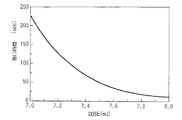
例えば、0.15μmL/Sパターンの露光条件(NA:0.6、露光波長:248nm、σ:0.75)では、レジスト110上に0次回折光しか到達しないような露光用マスクパターンのピッチは0.22μmとなる。そして、モニタエリア701の現像速度が2nm/sec(60秒の現像で膜厚が30nmになる)となる露光量が7.2mJである場合において、デバイスパターン111の最適露光量が20mJであるとすると、前記透過率は36%となる。
【0115】
従って、この場合、ピッチが0.22μmで、ライン幅が透過率が36%となるように設計されているライン系パターンをモニタエリア701形成用の露光用マスクパターンとして採用することで、所望のモニタエリア701を形成することができる。
【0116】
次に、このようなモニタエリア701を用いて、現像をモニタする装置構成について、図21を参照して説明する。
【0117】
この図21において、ウエハ(被処理基板)100上のレジスト110には、デバイスパターン111と共にこの実施形態のモニタエリア701が、前述した一括露光により形成されている。このモニタエリア701は、1ショット内においてデバイス作成に寄与するエリアと分離して配置されている。
【0118】
また、この装置は、前記第2の実施形態のものと同様に、現像中に適用される寸法モニタ装置であるから、レジスト110上には現像液230が存在する。
【0119】
この装置は、光源702から波長410nm(半値幅5nm)に狭帯化したほぼ単色の平行光を前記モニタエリア701に入射させる。そしてモニタエリア701からの0次回折光は0次回折光検出器(CCDカメラ)703により検出するようになっている。
【0120】
前記光源702及び0次回折光検出器703は、制御部704に接続されおり、この制御部704からの作動信号に基づいて動作する。すなわち、まず、前記制御部704は、0次回折光検出器703による0次回折光の検出に基づいて、光源及702及び0次回折光検出器703を前記モニターエリア701に対向する位置に駆動・位置決めする。そして、現像の開始に伴い、前記0次回折光検出器704を用いたモニタを開始する。
【0121】
このモニタは、前記モニタエリア701からの0次回折光の強度を検出することで行う。すなわち、理想的な場合、モニタエリア701の膜厚に対する0次回折光の強度変化は図22に示すように、極大点I'max、極小点I'minを有するカーブで表される。ここで、現像終点となる膜厚での0次回折光の強度をI'endとすると、I'endは、極大点I'max、極小点I'minを用いて次のように表せる。
【0122】
【数2】
ここで、aは補正係数であり、予め先行ウエハ等を用いて測定した極大、極小における0次回折光強度Imax,Imin、Iendと、現在の現像で測定した極大、 極小における0次回折光強度I'max,I'minとから求められる。この補正係数aを現在の測定値I'max,I'minに適用することで、現像終了点の0次回折光強度I'endを求めることができる。そして、前記現像終点予測部220’は、前記0次回折光検出器703により検出された光強度がI'endとなった時点で現像を終了させる。
【0124】
なお、この実施例で重要なことは、前述のように0次回折光の強度変化の極大、極小に基づいて現像終了時点を予測している点である。したがって、前記光源702から発振される観察光として、このような極大、極小が得られるような波長を有するものを選択して用いる必要がある。
【0125】
なお、この例では、現像終了の判断と実際の現像終了との間に極端な時間差がないものとして説明しているが、無視できない時間差が存在する場合は、モニタエリア701に対する露光強度としてその時間差に相当する分を差し引いた強度を設定すれば良い。
【0126】
このような構成によれば、モニタエリア701からの0次回折光の強度変化をモニタすることで現像時間を制御できるから、第1〜第8の実施形態と同様の効果を得ることができる。
【0127】
また、この実施形態によれば、パターンを持たないモニタエリア701を用いることで、以下に説明する効果を得ることができる。
【0128】
すなわち、この実施形態では、パターンを有しないモニタエリア701からの0次回折光をモニタすると共に、光強度の極大、極小に基づいて現像終了点を予測するようにした。このような構成によれば、光強度信号にオフセットが生じた場合であっても、光強度の絶対値ではなく、既知の極大、極小、現像終点に基づいて求めた補正係数を現在の測定値に適用することで現像終点を正確に予測できる。
【0129】
これに対して、第1〜第8の実施形態では、0次回折光の強度信号の絶対値を用いてモニタを行っている。このような方法では、何らかの原因で信号にオフセットが生じた場合に、デバイスパターンの現像終点を正確に検出できない恐れがある。また、入射光をモニタパターンの直上から照射し、その0次回折光を検出する構成では、強度信号がパターンの残り面積を反映してしまうため、0次回折光の強度は、図12に示すように現像時間に対して直線的に変化することになる。したがって、この場合も、強度信号の絶対値を用いてモニタすることになってしまい、やはり現像終点を正確に検出できない恐れが生じる。
【0130】
この実施形態の制御によれば、この様な欠点を排除し、上述したように、より正確に現像終点を検出できる効果がある。
【0131】
なお、この第9の実施形態では、パターンを有しないモニタエリア701を使用したが、このモニタエリアの形成方法はこの実施形態に挙げたものに限定されるものではなく、適宜他の方法を用いて形成するようにしても良い。たとえば、この実施形態では、所定のピッチ、線幅を有する露光パタンを用いた露光により前記モニタエリア701を形成するようにしたが、透過率を適宜に設定したハーフトーン膜を露光マスクとして形成するようにしても良い。
【0132】
(第10の実施形態)
この実施形態は、第9の実施形態の具体例を示すものである。
【0133】
図23はこの実施形態を示す概略構成図である。
【0134】
まず、この実施形態では、前記光源702は、グレーティングにより分光可能なランプハウス801と、このランプハウス801に接続された光ファイバ802と、この光ファイバ802の先端に取り付けられたコリメーションレンズ803とからなる。前記光ファイバ802の先端部及びこのコリメーションレンズ803は、XYZ方向に移動可能なモニタヘッド804により保持されている。
【0135】
前記ランプハウス801からの平行光は、光ファイバ802、コリメーションレンズ803を通して前記モニタエリア701に入射する。このモニタエリア701からの0次回折光は、前記モニタヘッド804に保持されたレンズ805、このレンズ805に接続され先端部を前記モニタヘッド804に保持された光ファイバ806を通して前記0次回折光検出器703(CCDカメラ)に検知されるようになっている。
【0136】
前記モニタヘッド804は、モニタヘッド駆動装置807によって駆動されるようになっていて、このモニタヘッド駆動装置807は、前記制御部704の指令により作動するように構成されている。
【0137】
すなわち、このモニターヘッド804はモニターエリア701の位置に移動し、モニターエリア701からの0次回折光の強度を検出する。このとき、モニターヘッド804はウエハのショットマップおよびマスクのレイアウトをもとにモニターエリア701に移動し、その後は、現像中のウエハの回転に同期させてモニターエリア701の強度を取得する。
【0138】
なお、この際、複数のモニタヘッドを用いるようにして、検出精度を高めるようにしても良い。また、モニタヘッド804は、図13(a)〜(c)や図5に示すような配置であっても良い。また、モニタヘッド804の形状も、図13に示した形状のものの他、適宜の形状を採用することが可能である。
【0139】
(第11の実施形態)
この実施形態は、第9の実施形態、第10の実施形態と同様に、現像中にモニタエリア701からの0次回折光をモニタし、現像終了時点を判断する装置である。ただし、第9の実施形態では現像の終了点を0次回折光の強度に基づいて判断したが、この実施形態では、現像時間に基づいて判断する。その他の点は、第9若しくは第10の実施形態と同様であるから説明を省略する。
【0140】
図24は、レジスト110の膜厚と0次回折光の強度の関係を示すグラフである。この実施形態では、光強度が極大、極小となる現像時刻t'max、t'minから、現像終点となる現像時刻t'endを予測し、この現像時刻t'endで現像を終了させるようにしたものである。
【0141】
なお、プロセス条件が常に一定であれば、現像終点となる時刻は一定である。しかし、実際にはプロセス条件にはゆらぎがあるため、現像終了時刻は一定にはならない。今、露光量の条件が所望の値の−5%変動したとすると、現像時間に対するレジスト膜の膜減りはレジストの溶解特性より図25に示す通りに変化する。このときの極小値、極大値、現像終点となる時間をそれぞれ、t'max、t'min、t'endとする。そして、この実施形態では、次式に示すように、予め求めておいた現像終了時刻tendに補正係数aをかけることで、現在の現像プロセスに おける現像終了時刻t'endを予測する。
【0142】
t'end=a×tend
補正係数aは、次式で求められるもののうちもっとも精度が良いものを用いるようにすれば良い。
【0143】
a=t'max/tmax
a=t'min/tmin
a=(t'max/tmax+t'min/tmin)/2
なお、現像終了時刻t'endの定め方はこの方法に限定されるものではなく、極値となる時刻時間t'max、t'minに基づいて予測するものであれば、例えばt'maxから一定の時間の後を現像終了時刻とする等、適宜の方法を採用することが可能である。
【0144】
(第12の実施形態)
この実施形態は、第9、第10の実施形態と同様にモニタエリアからの0次回折光をモニタするものであるが、互いに異なる波長を有する2種類の観察光を用いてモニタを行うものである。
【0145】
すなわち、この実施形態では、図23に示す構成において、ランプハウス801から、波長410nm(半値幅5nm)に狭帯化した光と波長600nm(半値幅5nm)に狭帯化した光を交互に出射するように制御する。
【0146】
制御部704は、前記CCDカメラ703により、両方の波長の0次回折光の強度を交互に検出する。理想的な場合、各波長でのレジスト膜厚に対する0次回折光の強度変化は図26に示すようになる。
【0147】
ここで、波長410nmの場合の極大、極小、現像終点での0次回折光の強度をI1max、I1min、I1end、波長600nmの場合の極大、極小となる強度をI2max、I2minとする。一方、今回の現像で検出された波長410nmの場合の極大、極小での0次回折光の強度をI1'max、I1'min、波長600nmの場合の極大、極小となる強度をI2'max、I2'minとすると、現像終点の強度I'endは、補正係数aを用いて次式で求められる。
【0148】
【数3】
この様な構成によれば、異なる波長の光を用い、一方の波長の光の検出値に加えて他方の波長の光の測定値を用いて補正を行うようにしたから、現像終了時点の0次回折光強度をより精度良く予測することが可能になる。
【0150】
なお、この実施形態のように2つの異なる波長を用いて補正精度を挙げる手法は、第11の実施形態に示したように極大、極小となる時刻tmax、tminから、現像終了となる時刻tendを予測する方法にも適用できる。
【0151】
すなわち、理想的な場合、410nm、470nmの各波長を有する光でのレジスト膜厚に対する0次回折光の強度変化は図27に示すようになる。
【0152】
このとき、波長410nmの光の0次回折光強度が極小、極大、現像終点となる時刻をそれぞれ、t1max、t1min、tendとする。また、波長470nmの光 の0次回折光強度が極大となる時刻をt2maxとする。プロセス条件が常に一定であれば、現像時間は常に一定でよいが、実際にはプロセス条件にゆらぎがある。今、露光量の条件が所望の値の−5%であったとすると、現像時間に対する膜減りはレジストの溶解特性より図28に示すようになる。
【0153】
このとき、波長410nmの光の0次回折光強度が極小、極大、現像終点となる時間をそれぞれ、t1'max、t1'min、t'endとし、波長470nmの光の0次回折光強度が極大となる時刻をt2'maxとする。これらの時間のうちあらかじめ t1max、t1min、tend、t2maxは求められており、現像中に0次回折光を検出 することにより、t1'max、t1'min、t2'maxが算出される。これらより次の式 で現像終了点の時間t'endを求めることができる。
【0154】
t'end=a×tend
a=(t1'max/t1max+t1'min/t1min+t2'max/t2max)/3
したがって、第11の実施形態と同様に、時刻t'endで現像を終了するようにすれば、現像の終点を正確に制御できる。
【0155】
(第13の実施形態)
この実施形態は、第9の実施形態と同じように、モニタエリア701からの0次回折光をモニタするものであるが、レジスト110として、図29に示すように、現像開始当初は膜減りが起こらず、数秒後から膜減りが開始するような溶解特性を有するものを採用する。
【0156】
このモニタエリア701は、前記デバイスパターン111の現像終了時に膜減りが開始するように設計する。すなわち、60秒の現像した後に膜減りが始まるような露光量が6.6mJであるレジストを用いる場合、デバイスパターン111の最適露光量が30mJであるので、デバイスパターン用露光マスクと比較して透過率が22%となるようにモニタエリア用の露光マスクを設計する。
【0157】
図30にモニタエリア701に対する膜抜け時間と露光量との関係、図31にモニタエリア701に対する膜抜け開始時間と露光量との関係を示す。
【0158】
プロセス条件が常に一定であれば、現像時間は常に60秒で制御すればよいが、デバイスパターン111の露光量が適正値の30mJから29mJに変化した場合には、60秒では十分な現像が行なえないことになる。しかしながら、この実施形態では、モニタエリア701の膜抜け開始時点を検出することで、このようなプロセス条件の変動にも対応でき、常に正確な終点制御を行なえる。
【0159】
すなわち、デバイスパターン111の露光量が適正値の30mJから29mJに変化した場合、モニタエリア701の露光量はその22%であることから、モニタエリア701に対する露光量は6.4mJとなる。従ってこの場合、図31より、80秒後に膜抜けが開始する。したがって、この膜抜けを検出して現像の終点とすることで、プロセス条件の変動にも対応することができる。
【0160】
なお、膜の抜け始め及び抜け終わりの検出は、0次回折光の強度の変化に基づいて検出するようにすれば良い。
【0161】
また、同様の手法で図30に示す抜け終わり時間に基づいて、この抜け終わりを検出することで現像の終点とするようにしても良い。
【0162】
この場合、前記モニタエリア701は、前記デバイスパターン111の現像終了時に膜厚がほとんど0となるように設計する。すなわち、60秒の現像した後に膜厚がほとんど0若しくは0となるような露光量が7.5mJであるレジストを用いる場合、デバイスパターン111の最適露光量が30mJであるので、デバイスパターン用露光マスクと比較して透過率が25%となるようにモニタエリア用の露光マスクを設計する。
【0163】
前述したように、図30はモニタエリア701に対する膜抜け時間と露光量との関係を示すものである。
【0164】
プロセス条件が常に一定であれば、現像時間は常に60秒で制御すればよいが、デバイスパターン111の露光量が適正値の30mJから29mJに変化した場合には、60秒では十分な現像が行なえないことになる。しかしながら、この実施形態では、モニタエリア701の膜抜け時点(膜厚0)を検出することで、このようなプロセス条件の変動にも対応でき、常に正確な終点制御を行なえる。
【0165】
すなわち、デバイスパターン111の露光量が適正値の30mJから29mJに変化した場合、モニタエリア701の露光量はその25%であることから、モニタエリア701に対する露光量は7.25mJとなる。従ってこの場合、図30より、110秒後に膜抜けが終了する。したがって、この膜抜けを検出して現像の終点とすることで、プロセス条件の変動にも対応することができる。
【0166】
(第14の実施形態)
この実施形態は第9の実施形態と同様の構成を有する寸法モニタ装置を用い、図32に示すように、各ホールの中心が成六角形の各頂点に位置するように配置してなるモニタパターン901をモニタする装置に関するものである。
【0167】
このモニタパターン901は、他の実施形態のものと同様に、1ショット内においてデバイス作成に寄与するエリアと分離して10×10μm2のエリアに配 置されている。
【0168】
図33に、現像時間とモニタパターン901からの0次回折光の強度との関係を示す。この実施形態のモニタパターン901の場合、現像終点(60秒後)での強度変化は余り大きくならないため、現像終点の直接検出は困難である。このため、この実施形態では、現像初期の強度変化の大きい部分を0次回折光検出器で強度検出し、その検出値から現像終点を予測するようにする。予測方法としては、例えば、強度のしきい値を140に設定し、このしきい値を超えた後50秒後を現像の終点とする。
【0169】
このような構成によれば、現像終点で強度変化の少ないパターンを用いた場合でも、比較的正確に現像の終点を検出することができる効果がある。
【0170】
なお、本発明は上述した第1〜第14の各実施形態に限定されるものではない。例えば、モニタパターンを構成する要素パターンの形状、繰り返しピッチ、繰り返し数等は、仕様に応じて適宜変更可能である。モニタパターンは、デバイスパターンに隣接してチップ有効部の空き領域に形成しても良いし、チップのダイシングライン等に形成しても良い。
【0171】
モニタパターンに照射する光は実施形態に用いたものに何等限定されるものではなく、レジストを感光しない波長の単波長光(若しくは狭帯域の光)であればよい。現像後のパターン検査においては、レジストを感光させない波長である必要はない。モニタパターンからの回折光を検出する手段は、CCDカメラに限定されず、強度変化を検出できるものであればよい。
【0172】
また、実施形態では、斜め照射で垂直方向に1次回折光の検出、又は垂直照射で垂直方向に0次回折光の検出を行ったが、斜め照射で斜め方向に0次回折光の検出、又は垂直照射で斜め方向に1次回折光の検出を行うようにしても良い。また、レジストに対する露光は必ずしも光に限らず、X線或いは電子ビームを用いることも可能である。
【0173】
また、その他、本発明の要旨を逸脱しない範囲で、種々変形して実施することができることはいうまでもない。
【0174】
【発明の効果】
以上詳述したように本発明によれば、現像中又は現像後に、デバイスパターンや既加工パターンとは異なるモニタパターン、特に現像時間の経過によるに回折光の強度変化が大きいモニタパターンを用いてパターン評価を行うことにより、レジストパターンを短時間で高精度に検査することが可能となり、さらにこの検査を基に現像時間を制御することによって異なるウエハに対してもレジストパターンの精密な寸法制御が可能となる。
【図面の簡単な説明】
【図1】第1の実施形態を説明するためのもので、1次回折光を利用して現像後のパターン検査を行う際の装置構成例を示す図。
【図2】第1の実施形態におけるモニタパターンの例を示す図。
【図3】第1の実施形態における現像時間と1次回折光強度の関係を示す図。
【図4】理想的なピッチとライン幅の比と1次回折光回折強度との関係を示す図。
【図5】第2の実施形態を説明するためのもので、1次回折光を利用して現像中にパターン検査を行う際の装置構成例を示す図。
【図6】第2の実施形態におけるデバイスパターンとモニタパターンの例を示す図。
【図7】パターンの繰り返しピッチと検出角との関係を示す図。
【図8】第3の実施形態におけるデバイスパターンとモニタパターンの例を示す図。
【図9】第4の実施形態におけるモニタパターンと既加工パターンの例を示す図。
【図10】第5の実施形態を説明するためのもので、0次回折光を利用して現像中にパターン検査を行う際の装置構成例を示す図。
【図11】第5の実施形態におけるモニタパターンの例を示す図。
【図12】第5の実施形態における現像時間と0次回折光強度との関係を示す図。
【図13】第6の実施形態を説明するためのもので、0次回折光を利用して現像中にパターン検査を行う際の装置構成例を示す図。
【図14】(a)〜(c)は、第6の実施形態におけるモニタパターンの例を示す図。
【図15】(a)、(b)は、第6の実施形態におけるモニタヘッドの位置決めを示す図。
【図16】(a)〜(c)は、第6の実施形態におけるモニタパターンの検出例を示す図。
【図17】第7の実施形態を説明するためのもので、0次回折光を利用して現像中にパターン検査を行う際の装置構成例を示す図。
【図18】(a)、(b)は、第7の実施形態において、0次回折光の光路を説明するための図。
【図19】第8の実施形態を説明するためのもので、0次回折光を利用して現像中にパターン検査を行う際の装置構成例を示す図。
【図20】第9の実施形態を説明するためのもので、この実施形態で用いるモニタエリアを示す概略図。
【図21】第9の実施形態を説明するためのもので、0次回折光を利用して現像中にパターン検査を行う際の装置構成例を示す図。
【図22】第9の実施形態において、図20に示すモニタエリアからの0次回折光の強度とレジスト厚との関係を示す図。
【図23】第10の実施形態を説明するためのもので、0次回折光を利用して現像中にパターン検査を行う際の装置構成例を示す図。
【図24】第11の実施形態を説明するためのもので、図20に示すモニタエリアからの0次回折光の強度とレジスト厚との関係を示す図。
【図25】第11の実施形態を説明するためのもので、レジスト厚と現像時間との関係を示す図。
【図26】第12の実施形態を説明するためのもので、2つの異なる波長の光を用いて検出した場合の0次回折光の強度とレジスト厚との関係を示す図。
【図27】第12の実施形態の他の測定例を説明するためのもので、2つの異なる波長の光を用いて検出した場合の0次回折光の強度とレジスト厚との関係を示す図。
【図28】第12の実施形態の他の測定例を説明するためのもので、2つの異なる波長の光を用いて検出した場合のレジスト厚と現像時間との関係を示す図。
【図29】第13の実施形態を説明するためのもので、レジスト厚と現像時間との関係を示す図。
【図30】第13の実施形態を説明するためのもので、露光量とレジストの抜け時間との関係を示す図。
【図31】第13の実施形態を説明するためのもので、露光量とレジストの抜け始め時間との関係を示す図。
【図32】第14の実施形態で用いるモニタパターンの例を示す図。
【図33】第14の実施形態を説明するためのもので、0次回折光の強度と露光時間との関係を示す図。
【符号の説明】
100…ウエハ
110…レジスト
111…デバイスパターン
112…モニタパターン
201、301…入射光
202、302…0次回折光
203、303…1次回折光
210…CCDカメラ
220…パターン寸法評価部
220’…現像終点予測部[0001]
BACKGROUND OF THE INVENTION
The present invention relates to a photolithography resist pattern formation technique in the manufacture of a semiconductor device, and in particular, pattern dimension evaluation for evaluating a resist pattern during or after development. Method and pattern forming method It is about.
[0002]
[Prior art]
In order to form an integrated circuit pattern on a wafer, after applying a resist on the wafer, the resist is exposed to a desired pattern, and further developed to form a resist pattern, which is then used as a mask for processing such as etching. Do. Although a high dimensional accuracy is required for the resist pattern as a mask, the dimension of the resist pattern varies greatly depending on the development time. For this reason, control of the development time is very important.
[0003]
Conventionally, the dimension control at the time of development has been carried out with the development time of all wafers being fixed by determining the optimum development time by exposing and developing the preceding wafer and then evaluating its dimensions. However, since the wafer histories such as the holding time of each wafer are actually different, if the same lot is developed in the same development time, dimensional variation occurs between the wafers, and development can be completed with a desired dimension. Can not.
[0004]
Until now, even if such development time management was performed, the dimensional error was within the allowable range, which was not a big problem. However, the process has been miniaturized and dimensional control is more precise than ever. Therefore, it is difficult to control the dimensions during development by the conventional development time management method.
[0005]
On the other hand, conventionally, evaluation of a resist pattern performed after development has been performed using, for example, an SEM (Scanning Electron Microscope). The SEM can observe a high-magnification pattern, but the apparatus configuration is complicated and expensive. Further, since a very long time is required for the inspection, it is difficult to evaluate efficiently.
[0006]
In addition, not only during and after development, but also when optically inspecting a device pattern using diffracted light, etc., information from other device patterns may be captured when monitoring the required device pattern This was a factor that deteriorated the accuracy of the monitor.
[0007]
[Problems to be solved by the invention]
As described above, it has been conventionally difficult to precisely control the resist pattern on different wafers by controlling the development time. In addition, there is a problem that it takes a lot of time to evaluate the resist pattern by SEM. Further, when a device pattern is inspected using diffracted light or the like, there is a problem that the monitoring accuracy is lowered due to an influence from a pattern different from the pattern to be monitored.
[0008]
The present invention has been made in consideration of the above circumstances, and its purpose is to perform pattern dimension evaluation that enables precise dimension control of resist patterns even on different wafers. Method and pattern forming method Is to provide.
[0009]
Another object of the present invention is to provide a pattern dimension evaluation that can inspect a resist pattern with high accuracy in a short time without being affected by a pattern different from the pattern to be monitored. Method and pattern forming method Is to provide.
[0010]
Still another object of the present invention is to evaluate the dimension of a resist pattern, which can evaluate the dimension of a resist pattern in a short time and with high accuracy during development, and can predict the end point of development with high accuracy. Method and pattern forming method Is to provide.
[0011]
[Means for Solving the Problems]
(Constitution)
The pattern evaluation method according to one aspect of the present invention for solving the above-described problem is to form a device pattern and a monitor pattern by exposing a resist film on a substrate to be processed and developing the resist film, Is a pattern dimension evaluation method for evaluating the size of the resist film on the basis of the diffracted light intensity of the light irradiated on the monitor pattern, and the resist film is formed in one shot using a mask comprising a device mask pattern and a monitor mask pattern. Exposing and transferring the device mask pattern and the monitor mask pattern to the resist film; developing the exposed resist film to form the device pattern and the monitor pattern; and Or, after development, parallel light of a predetermined wavelength is emitted from the monitor pattern. Comprising the step of irradiating, detecting the diffracted light intensity from the monitor pattern, and a step of evaluating the size of the device pattern based on the diffracted light intensity from the monitor pattern, said monitor mask The pattern is Circular or polygonal pattern is two-dimensionally periodic Arranged, And by being arranged so that the pattern interval is below the resolution limit of the exposure apparatus used, For developing the monitor pattern when the monitor pattern and the device pattern are irradiated with light of a predetermined wavelength during or after the development. Accompany A change in the diffracted light intensity is formed so as to be larger than a change in the diffracted light intensity with respect to a dimensional change caused by development of the device pattern.
[0019]
(Function)
In the present invention, the dimension of the resist pattern can be inspected by performing pattern evaluation using a monitor region composed of elements that can be identified from the device pattern and the already-processed pattern during or after development of the resist.
[0020]
When a monitor pattern is formed in the monitor region by exposure, for example, an exposure mask configured to use a circle or a polygon as an element pattern of the exposure mask, and the pattern interval is equal to or less than the resolution limit of the exposure apparatus to be used. Use for exposure. According to the monitor pattern thus formed, the change in the intensity of the diffracted light with the lapse of the development time can be made larger than that of the device pattern, and thereby the inspection accuracy can be improved.
[0021]
In addition, by performing pattern evaluation using monitor patterns having different pitches or repetition directions, it is possible to perform inspection with high accuracy without being affected by other patterns. Furthermore, since pattern evaluation can be performed only by monitoring the diffracted light intensity, SEM or the like is different and inspection can be performed in a short time.
[0022]
On the other hand, the monitor area does not have the pattern as described above, but is exposed so as to have a substantially uniform development speed over the entire area, and is formed so that the film thickness is reduced substantially uniformly as the development proceeds. In the case of using the sensor, the maximum and minimum of the diffracted light intensity from the monitor region can be observed. The development end point of the device pattern can be predicted based on the maximum and minimum.
[0023]
According to such a prediction method, even if a signal-like offset occurs in the absolute value of the diffracted light intensity signal, the development end point of the device pattern is predicted based on the maximum and minimum, It is possible to obtain an accurate development end point by correcting this offset.
[0024]
DETAILED DESCRIPTION OF THE INVENTION
The details of the present invention will be described below with reference to the illustrated embodiments.
[0025]
(First embodiment)
FIG. 1 is a diagram for explaining a pattern dimension evaluation apparatus according to a first embodiment of the present invention, and is a diagram showing an apparatus configuration example for performing pattern inspection after development using first-order diffracted light.
[0026]
A
[0027]
Parallel light having a wavelength of 400 ± 20 nm is incident on the
[0028]
FIG. 2 is a diagram showing an example of the
[0029]
As the
[0030]
Then, under the condition that the 0.15 μm L & S device pattern (line width: space width = 1: 1) 111 was finished to a desired dimension in a development time of 30 seconds, the
(A)... Monitor pattern shown in FIG.
[0031]
(B)... 0.15 μm L & S monitor pattern (line width: space width = 1: 1).
[0032]
(C) 0.15 μm L & S monitor pattern (finished line width: space width = 1: 3).
[0033]
(D) An L & S monitor pattern having a line width of 0.07 μm and a space width of 0.2 μm.
[0034]
Here, since (b) has the same dimensions as the
[0035]
The relationship of the first-order diffracted light intensity after development with respect to each of the development times (10 to 36 seconds) of (a) to (d) is as shown in FIG. At this time, since the pattern (d) was not resolved at all, it is not shown.
[0036]
In the vicinity of the development end point (30 seconds), there was almost no change in intensity in the pattern (b), and the monitor pattern in (a) showed an intensity change about four times that in the pattern in (c). At this time, the intensity change of the monitor pattern of (a) is 10 (CCD camera) with respect to the change of the dimension 1.5 nm of the 0.15 μm L & S pattern (line width: space width = 1: 1) of (b). The gradation is 256).
[0037]
The cause is as follows.
[0038]
The pattern repeat pitch is p, the interval between line parts, the reflectivity, the phase is l, r a , Φ a , Space part reflectivity, phase r b , Φ b Then, as shown in (HP Kleinknecht and H. Meier, Applied Optics Vol.19 No.4 (1980) pp525-533), the intensity of the m-th order light in the L & S pattern is expressed by the following equation.
[0039]
[Expression 1]
From this relationship, in order to obtain a large intensity change, it is necessary that the line width change occurs in the vicinity of 1 / p = 0.25 or 0.75 (FIG. 4).
[0041]
That is, in the monitor pattern (a), the change in the line width occurs in the vicinity of 1 / p = 0.25, and therefore, the change is considered to be the largest. Further, since the L & S pattern of (d) having the same pitch as that of the pattern of (a) but having a different space width shows no change, it is considered that the hole-like pattern is important.
[0042]
As described above, according to the present embodiment, when pattern evaluation is performed from the first-order diffracted light intensity after development, a monitor pattern having a larger first-order diffracted light intensity change than the dimensional change of the
[0043]
That is, in the 0.15 μm L & S pattern (line width: space width = 1: 1) of the
[0044]
In addition, since the pattern evaluation is performed by an optical method, the wafer pattern can be easily evaluated, and the throughput is improved. Furthermore, if monitoring is performed with a 1024 gradation CCD camera, it is possible to simply monitor with four times the accuracy.
[0045]
(Second Embodiment)
FIG. 5 is a diagram for explaining a second embodiment of the present invention, and is a diagram showing an apparatus configuration example when pattern inspection is performed during development using first-order diffracted light. That is, this is an example of an in-situ development monitor using first-order diffracted light.
[0046]
The basic configuration is the same as in FIG. 1 except that a
[0047]
Also in this apparatus, during development,
[0048]
Specifically, as shown in FIG. 6, the
[0049]
On the other hand, as the
[0050]
First-order diffracted light 203 from the
[0051]
In this embodiment, since the pattern pitches of the
[0052]
That is, when the incident angle in FIG. 5 is 40 °, the relationship between the detection angle and the pattern pitch is expressed as shown in FIG. According to this figure, the detection angle when the pitch is 0.27 μm is 57 °, and the detection angle when the pitch is 0.30 μm is 44 °. Therefore, even if the
[0053]
As described above, according to the present embodiment, by using the
[0054]
(Third embodiment)
The present embodiment has the same device configuration (FIG. 5) as the second embodiment, but the arrangement of the
[0055]
In this apparatus,
[0056]
Specifically, as shown in FIG. 8, there are L &
[0057]
Here, the first-order diffracted light 203 from the
[0058]
When light is incident on the pattern surface at an angle of about 30 ° from the direction indicated by the arrow (α) in FIG. 8, the first-order diffracted light from the
[0059]
According to the present embodiment, by using the
[0060]
(Fourth embodiment)
This embodiment also has the same apparatus configuration (FIG. 5) as the second embodiment, but the arrangement of the
[0061]
Also in this apparatus,
[0062]
As the
[0063]
First-order diffracted light 203 from the
[0064]
The incident angle of incident light in FIG. 5 is 40 °, and the relationship between the detection angle and the pitch is expressed as shown in FIG. The detection angle when the pitch is 0.27 μm is 57 °, and the detection angle when the pitch is 0.30 μm is 44 °. Therefore, if a different monitor pattern is used for each layer, the
[0065]
According to the present embodiment, since monitor patterns having different pitches for each layer are used as the monitor pattern, it is possible to perform accurate monitoring without being affected by the first-order diffracted light from the lower layer monitor pattern. In the same manner as described above, precise dimensional control of the resist pattern can be performed.
[0066]
(Fifth embodiment)
FIG. 10 is a diagram for explaining a fifth embodiment of the present invention, and is a diagram showing an example of a device configuration when pattern inspection is performed during development using 0th-order diffracted light. That is, this is an example of an in-situ development monitor using 0th-order diffracted light.
[0067]
In this apparatus, a
[0068]
FIG. 11 shows the
[0069]
As the
[0070]
FIG. 12 shows the relationship between development time and 0th-order diffracted light intensity. At the development end time of 30 seconds for the device pattern, the change in 0th-order diffracted light intensity in the
[0071]
The reason why a large change in intensity was obtained in the monitor pattern is as follows: (1) The shape change of the hole pattern is larger in the outer circumference direction of the circle, and (2) The holes are densely arranged. For example, the area surrounded by three adjacent hole patterns is below the resolution limit, and (3) the shape of the undeveloped portion is tapered.
[0072]
When the CCD camera is used by using the development monitor pattern (L = 0.2 μm, dx = dy = 0.06 μm) shown in FIG. 11, the dimensional change (1.5%) of the 0.15 μm L & S pattern is 1%. ) Can be monitored with 6 gradations, and the line width can be controlled more precisely as compared with 2 gradations in the case of the 0.15 μm L & S pattern. If a CCD camera with 1024 gradations is used, the line width can be controlled more precisely.
[0073]
(Sixth embodiment)
FIG. 13 (a) is a schematic configuration diagram showing a sixth embodiment of the present invention. In addition, the same code | symbol is attached | subjected about the component same as embodiment already described (refer especially 2nd Example), and the description is abbreviate | omitted.
[0074]
In the figure,
[0075]
The
[0076]
In the example of FIG. 13A, the
[0077]
FIGS. 13B and 13C show other arrangement examples of the
[0078]
The
[0079]
As the
[0080]
In this embodiment, the incident angle of incident light with respect to the monitor pattern 112 (all the angles shown below are angles with respect to the monitor pattern 112) is 60 °, the detection angle of the first-order diffracted light (107) from the
[0081]
Next, the operation of this apparatus will be described.
[0082]
In FIG. 15A,
[0083]
The
[0084]
Therefore, the first-order diffracted
[0085]
On the other hand, as shown in FIG. 16B, the 0th-order diffracted
[0086]
If the above detection is performed, the control device 407 moves / rotates the
[0087]
According to such an embodiment, an
[0088]
Note that the control device 407 (development end
[0089]
Thus, by simultaneously monitoring the 0th-order diffracted light and the 1st-order diffracted light, the measurement accuracy is further improved.
[0090]
Of course, the
[0091]
Also,
(Seventh embodiment)
FIG. 17 is a schematic configuration diagram showing this embodiment. In addition, the same code | symbol is attached | subjected to the component same as 6th Embodiment, and the detailed description is abbreviate | omitted.
[0092]
The reflective
[0093]
The reflective
[0094]
Here, the incident angle of the incident light with respect to the
[0095]
According to such a configuration, first, by performing the same control as in the sixth embodiment, it is possible to monitor the 0th-order diffracted light from the
[0096]
That is, as shown in FIG. 18A, since there is incident light 505 corresponding to the top of the resist and incident light 506 corresponding to the resist pattern in oblique incidence, the 0th-order diffracted light does not directly reflect the remaining area of the resist.
[0097]
However, in this embodiment, as shown in FIG. 18B, since the incidence is normal, the intensity of the 0th-order diffracted light is expressed as the sum of the 0th-order diffracted light 507 from the resist and the 0th-order diffracted light 508 from the antireflection film. Is done. For this reason, the remaining area of the resist is directly reflected. Therefore, as compared with the sixth embodiment, since it is possible to acquire the light intensity reflecting the remaining area of the resist, it is possible to perform monitoring with higher accuracy.
[0098]
Also in the apparatus of this embodiment, various apparatus arrangements are conceivable as shown in FIGS. 13B and 13C. In addition, the monitor head shown in this embodiment may be applied to an apparatus that performs pattern dimension evaluation after development.
[0099]
(Eighth embodiment)
FIG. 19 is an apparatus configuration diagram showing this embodiment. In addition, about the structure similar to 6th, 7th embodiment, the same code | symbol is attached | subjected and the detailed description is abbreviate | omitted.
[0100]
The
[0101]
In this embodiment, the incident angle of incident light with respect to the monitor pattern 112 (all angles shown below are angles with respect to the monitor pattern) is 0 °, the detection angle of the first-order diffracted light from the
[0102]
According to such a configuration, development can be monitored by the same control as in the sixth embodiment. Further, since the optical path of the incident light to the
[0103]
Also in the apparatus of this embodiment, various apparatus arrangements are conceivable as shown in FIGS. 13B and 13C. Of course, the configuration shown in this embodiment can be applied to an apparatus for performing pattern dimension evaluation after development.
[0104]
(Ninth embodiment)
Ninth Embodiment In each of the following embodiments, monitoring is performed using a monitor area having a different form from the first to eighth embodiments. However, the same components as those of the first to eighth embodiments are denoted by the same reference numerals, and detailed description thereof is omitted.
[0105]
That is, in the first to eighth embodiments, the
[0106]
In this embodiment, the intensity of the 0th-order diffracted light from the
[0107]
Hereinafter, the procedure for forming the
[0108]
In this embodiment, the
[0109]
When exposure is performed using an exposure mask, the exposure conditions for only the 0th-order diffracted light from the exposure mask to reach the resist 110 are the exposure wavelength λ, the pitch p, NA, and σ of the mask pattern equivalent on the resist. Is defined as follows.
[0110]
λ / p ≧ (1 + σ) NA (2)
Therefore, the pitch of the pattern provided on the exposure mask for the
[0111]
In this embodiment, the exposure intensity for the resist 110 is controlled by appropriately setting the transmittance by adjusting the line width of the exposure mask, and the development speed of the
[0112]
Next, an exposure amount (exposure amount for forming the monitor pattern 701) corresponding to the development speed is calculated from the obtained development speed and the dissolution characteristics of the resist 110. Then, the transmittance of the exposure mask for the
[0113]
Therefore, on the exposure mask for the
[0114]
For example, under an exposure condition of 0.15 μmL / S pattern (NA: 0.6, exposure wavelength: 248 nm, σ: 0.75), the pitch of the exposure mask pattern that only reaches the 0th order diffracted light on the resist 110 is 0.22 μm. When the exposure amount at which the development speed of the
[0115]
Therefore, in this case, by adopting a line pattern designed to have a pitch of 0.22 μm and a line width of 36% as an exposure mask pattern for forming the
[0116]
Next, an apparatus configuration for monitoring development using such a
[0117]
In FIG. 21, a
[0118]
Further, since this apparatus is a dimension monitoring apparatus applied during development, as in the second embodiment, the
[0119]
In this apparatus, substantially monochromatic parallel light narrowed to a wavelength of 410 nm (half-
[0120]
The
[0121]
This monitoring is performed by detecting the intensity of the 0th-order diffracted light from the
[0122]
[Expression 2]
Here, a is a correction coefficient, and the 0th-order diffracted light intensity Imax, Imin, Iend at the maximum and minimum measured in advance using a preceding wafer or the like, and the 0th-order diffracted light intensity I ′ at the maximum and minimum measured by the current development. It is obtained from max and I'min. By applying this correction coefficient a to the current measured values I′max and I′min, the zero-order diffracted light intensity I′end at the development end point can be obtained. Then, the development end
[0124]
The important point in this embodiment is that the development end point is predicted based on the maximum and minimum of the intensity change of the 0th-order diffracted light as described above. Therefore, it is necessary to select and use the observation light oscillated from the
[0125]
In this example, it is described that there is no extreme time difference between the end of development and the actual end of development. However, when there is a time difference that cannot be ignored, the time difference is set as the exposure intensity for the
[0126]
According to such a configuration, since the development time can be controlled by monitoring the intensity change of the 0th-order diffracted light from the
[0127]
Further, according to this embodiment, the following effects can be obtained by using the
[0128]
That is, in this embodiment, the zero-order diffracted light from the
[0129]
On the other hand, in the first to eighth embodiments, monitoring is performed using the absolute value of the intensity signal of the 0th-order diffracted light. In such a method, when an offset occurs in the signal for some reason, there is a possibility that the development end point of the device pattern cannot be accurately detected. Further, in the configuration in which incident light is irradiated from directly above the monitor pattern and the 0th-order diffracted light is detected, the intensity signal reflects the remaining area of the pattern, so the intensity of the 0th-order diffracted light is as shown in FIG. It will change linearly with development time. Therefore, also in this case, monitoring is performed using the absolute value of the intensity signal, and there is a possibility that the development end point cannot be accurately detected.
[0130]
According to the control of this embodiment, it is possible to eliminate such drawbacks and to detect the development end point more accurately as described above.
[0131]
In the ninth embodiment, the
[0132]
(Tenth embodiment)
This embodiment shows a specific example of the ninth embodiment.
[0133]
FIG. 23 is a schematic configuration diagram showing this embodiment.
[0134]
First, in this embodiment, the
[0135]
Parallel light from the
[0136]
The
[0137]
That is, the
[0138]
At this time, a plurality of monitor heads may be used to improve detection accuracy. The
[0139]
(Eleventh embodiment)
As in the ninth and tenth embodiments, this embodiment is an apparatus that monitors the 0th-order diffracted light from the
[0140]
FIG. 24 is a graph showing the relationship between the film thickness of the resist 110 and the intensity of the 0th-order diffracted light. In this embodiment, the development time t′end that is the development end point is predicted from the development times t′max and t′min at which the light intensity becomes maximum and minimum, and the development is terminated at the development time t′end. It is a thing.
[0141]
If the process conditions are always constant, the time when the development end point is reached is constant. However, since the process conditions actually fluctuate, the development end time is not constant. Now, assuming that the exposure condition fluctuates by -5% of a desired value, the film thickness of the resist film with respect to the development time changes as shown in FIG. At this time, the minimum value, maximum value, and development end time are t′max, t′min, and t′end, respectively. In this embodiment, as shown in the following equation, the development end time t′end in the current development process is predicted by multiplying the previously determined development end time tend by the correction coefficient a.
[0142]
t'end = a × tend
As the correction coefficient a, the one having the highest accuracy among those obtained by the following equation may be used.
[0143]
a = t'max / tmax
a = t'min / tmin
a = (t′max / tmax + t′min / tmin) / 2
Note that the method of determining the development end time t′end is not limited to this method. For example, if the prediction is based on the extreme time t′max and t′min, for example, from t′max. It is possible to adopt an appropriate method such as setting the development end time after a certain time.
[0144]
(Twelfth embodiment)
In this embodiment, the 0th-order diffracted light from the monitor area is monitored as in the ninth and tenth embodiments, but monitoring is performed using two types of observation light having different wavelengths. .
[0145]
That is, in this embodiment, in the configuration shown in FIG. 23, light narrowed to a wavelength of 410 nm (
[0146]
The
[0147]
Here, the intensity of 0th-order diffracted light at the maximum, minimum, and development end point when the wavelength is 410 nm is expressed as I 1 max, I 1 min, I 1 end, the maximum and minimum intensities when the wavelength is 600 nm 2 max, I 2 Let min. On the other hand, the intensity of the 0th-order diffracted light at the maximum and minimum at the wavelength of 410 nm detected in this development is expressed as I 1 'max, I 1 'min, the maximum and minimum intensities when the wavelength is 600 nm 2 'max, I 2 Assuming that “min”, the development end point intensity I′end can be obtained by the following equation using the correction coefficient a.
[0148]
[Equation 3]
According to such a configuration, since light having different wavelengths is used and correction is performed using the measured value of the light of the other wavelength in addition to the detected value of the light of the one wavelength, 0 at the end of development. It becomes possible to predict the next diffracted light intensity with higher accuracy.
[0150]
Note that, as in this embodiment, the technique for increasing the correction accuracy by using two different wavelengths is as follows. From the time tmax and tmin when the maximum and minimum are reached as shown in the eleventh embodiment, the time tend at which the development ends is determined. It can be applied to the prediction method.
[0151]
That is, in an ideal case, the change in the intensity of the 0th-order diffracted light with respect to the resist film thickness with light having wavelengths of 410 nm and 470 nm is as shown in FIG.
[0152]
At this time, the time when the 0th-order diffracted light intensity of the light having a wavelength of 410 nm is minimum, maximum, and development end point is t, 1 max, t 1 Let min and tend. In addition, the time when the 0th-order diffracted light intensity of the light having a wavelength of 470 nm is maximized is t. 2 Let it be max. If the process conditions are always constant, the development time may be always constant, but actually the process conditions fluctuate. Now, assuming that the exposure amount condition is −5% of the desired value, the film reduction with respect to the development time is as shown in FIG. 28 from the dissolution characteristics of the resist.
[0153]
At this time, the time when the 0th-order diffracted light intensity of light having a wavelength of 410 nm is minimum, maximum, and development end point is t, 1 'max, t 1 Let 'min, t'end be the time at which the 0th-order diffracted light intensity of light with a wavelength of 470 nm is maximized. 2 'max. T of these times in advance 1 max, t 1 min, tend, t 2 max is determined, and by detecting zero-order diffracted light during development, t 1 'max, t 1 'min, t 2 'max is calculated. From these, the development end point time t'end can be obtained by the following equation.
[0154]
t'end = a × tend
a = (t 1 'max / t 1 max + t 1 'min / t 1 min + t 2 'max / t 2 max) / 3
Therefore, as in the eleventh embodiment, if the development is terminated at time t′end, the development end point can be accurately controlled.
[0155]
(13th Embodiment)
In this embodiment, as in the ninth embodiment, the 0th-order diffracted light from the
[0156]
The
[0157]
FIG. 30 shows the relationship between the film loss time and the exposure amount for the
[0158]
If the process conditions are always constant, the development time may be always controlled at 60 seconds. However, if the exposure amount of the
[0159]
That is, when the exposure amount of the
[0160]
It should be noted that the start and end of film removal may be detected based on a change in the intensity of the 0th-order diffracted light.
[0161]
Further, the end point of development may be determined by detecting the end of the omission based on the omission end time shown in FIG.
[0162]
In this case, the
[0163]
As described above, FIG. 30 shows the relationship between the film removal time and the exposure amount for the
[0164]
If the process conditions are always constant, the development time may be always controlled at 60 seconds. However, if the exposure amount of the
[0165]
That is, when the exposure amount of the
[0166]
(Fourteenth embodiment)
This embodiment uses a size monitoring device having the same configuration as that of the ninth embodiment, and as shown in FIG. 32, a monitor pattern is arranged so that the center of each hole is located at each vertex of the formed hexagon. The present invention relates to an apparatus for
[0167]
This
[0168]
FIG. 33 shows the relationship between the development time and the intensity of the 0th-order diffracted light from the
[0169]
According to such a configuration, there is an effect that the development end point can be detected relatively accurately even when a pattern having a small intensity change is used at the development end point.
[0170]
The present invention is not limited to the first to fourteenth embodiments described above. For example, the shape, repetition pitch, number of repetitions, etc. of the element pattern constituting the monitor pattern can be appropriately changed according to the specifications. The monitor pattern may be formed in an empty area of the chip effective portion adjacent to the device pattern, or may be formed on a chip dicing line or the like.
[0171]
The light applied to the monitor pattern is not limited to that used in the embodiment, and may be single wavelength light (or narrow band light) having a wavelength that does not expose the resist. In the pattern inspection after development, it is not necessary to have a wavelength that does not expose the resist. The means for detecting the diffracted light from the monitor pattern is not limited to the CCD camera, and any means can be used as long as it can detect the intensity change.
[0172]
In the embodiment, the first-order diffracted light is detected in the vertical direction by oblique irradiation, or the zero-order diffracted light is detected in the vertical direction by vertical irradiation. Thus, the first-order diffracted light may be detected in an oblique direction. Further, the exposure of the resist is not necessarily limited to light, and X-rays or electron beams can also be used.
[0173]
In addition, it goes without saying that various modifications can be made without departing from the scope of the present invention.
[0174]
【The invention's effect】
As described above in detail, according to the present invention, a pattern using a monitor pattern that is different from a device pattern or an already-processed pattern during development or after development, in particular, a monitor pattern in which the intensity change of diffracted light is large as the development time passes. By performing the evaluation, it is possible to inspect the resist pattern with high accuracy in a short time, and furthermore, by controlling the development time based on this inspection, it is possible to precisely control the size of the resist pattern even for different wafers. It becomes.
[Brief description of the drawings]
FIG. 1 is a diagram illustrating a configuration example of an apparatus when pattern inspection after development is performed using first-order diffracted light for explaining the first embodiment.
FIG. 2 is a diagram showing an example of a monitor pattern in the first embodiment.
FIG. 3 is a graph showing a relationship between development time and first-order diffracted light intensity in the first embodiment.
FIG. 4 is a graph showing a relationship between an ideal pitch / line width ratio and first-order diffracted light diffraction intensity.
FIG. 5 is a diagram illustrating an apparatus configuration example when pattern inspection is performed during development using first-order diffracted light for explaining the second embodiment.
FIG. 6 is a diagram showing an example of a device pattern and a monitor pattern in the second embodiment.
FIG. 7 is a diagram illustrating a relationship between a pattern repetition pitch and a detection angle.
FIG. 8 is a diagram showing an example of a device pattern and a monitor pattern in the third embodiment.
FIG. 9 is a diagram showing an example of a monitor pattern and a processed pattern in the fourth embodiment.
FIG. 10 is a diagram illustrating a configuration example of an apparatus when pattern inspection is performed during development using 0th-order diffracted light for explaining a fifth embodiment.
FIG. 11 is a diagram showing an example of a monitor pattern in the fifth embodiment.
FIG. 12 is a diagram showing the relationship between development time and 0th-order diffracted light intensity in the fifth embodiment.
FIG. 13 is a diagram illustrating an apparatus configuration example for performing pattern inspection during development using 0th-order diffracted light for explaining the sixth embodiment.
FIGS. 14A to 14C are diagrams showing examples of monitor patterns in the sixth embodiment.
FIGS. 15A and 15B are diagrams showing positioning of a monitor head in the sixth embodiment. FIGS.
FIGS. 16A to 16C are diagrams showing examples of monitor pattern detection in the sixth embodiment;
FIG. 17 is a diagram illustrating a configuration example of an apparatus when pattern inspection is performed during development using 0th-order diffracted light for explaining the seventh embodiment.
FIGS. 18A and 18B are views for explaining an optical path of zero-order diffracted light in the seventh embodiment.
FIG. 19 is a diagram illustrating an apparatus configuration example for performing pattern inspection during development using 0th-order diffracted light for explaining the eighth embodiment.
FIG. 20 is a schematic diagram for explaining a ninth embodiment and showing a monitor area used in this embodiment.
FIG. 21 is a diagram illustrating an apparatus configuration example for performing pattern inspection during development using 0th-order diffracted light for explaining the ninth embodiment.
22 is a diagram showing the relationship between the intensity of 0th-order diffracted light from the monitor area shown in FIG. 20 and the resist thickness in the ninth embodiment.
FIG. 23 is a diagram illustrating a configuration example of an apparatus when pattern inspection is performed during development using 0th-order diffracted light for explaining the tenth embodiment.
24 is a view for explaining the eleventh embodiment and shows the relationship between the intensity of the 0th-order diffracted light from the monitor area shown in FIG. 20 and the resist thickness. FIG.
FIG. 25 is a view for explaining the eleventh embodiment and showing the relationship between the resist thickness and the development time.
FIG. 26 is a diagram for explaining the twelfth embodiment and shows the relationship between the intensity of 0th-order diffracted light and the resist thickness when detection is performed using light of two different wavelengths.
FIG. 27 is a diagram for explaining another measurement example of the twelfth embodiment and is a diagram showing a relationship between the intensity of 0th-order diffracted light and the resist thickness when detection is performed using light of two different wavelengths.
FIG. 28 is a view for explaining another measurement example of the twelfth embodiment and showing a relationship between a resist thickness and a development time when detection is performed using light of two different wavelengths.
FIG. 29 is a view for explaining the thirteenth embodiment and showing the relationship between the resist thickness and the development time.
FIG. 30 is a diagram for explaining a thirteenth embodiment and showing a relationship between an exposure amount and a resist removal time;
FIG. 31 is a diagram for explaining a thirteenth embodiment and showing a relationship between an exposure amount and a resist removal start time;
FIG. 32 is a diagram showing an example of a monitor pattern used in the fourteenth embodiment.
FIG. 33 is a view for explaining the fourteenth embodiment and shows the relationship between the intensity of the 0th-order diffracted light and the exposure time.
[Explanation of symbols]
100 ... wafer
110 ... resist
111 ... Device pattern
112 ... Monitor pattern
201, 301 ... Incident light
202, 302 ... 0th order diffracted light
203, 303 ... 1st order diffracted light
210 ... CCD camera
220 ... Pattern dimension evaluation section
220 '... Development end point prediction section
Claims (8)
デバイスマスクパターンとモニタマスクパターンとを具備するマスクを用いて1ショットで前記レジスト膜を露光し、前記デバイスマスクパターンと前記モニタマスクパターンを前記レジスト膜に転写するステップと、
露光された前記レジスト膜を現像することによって、前記デバイスパターン及び前記モニタパターンを形成するステップと、
前記現像中又は現像後に、所定の波長の平行光を前記モニタパターンに照射するステップと、
前記モニタパターンからの回折光強度を検出するステップと、
前記モニタパターンからの回折光強度に基づいて前記デバイスパターンの寸法を評価するステップと、
を具備し、
前記モニタマスクパターンは、円形又は多角形のパターンが二次元的に周期的に配置され、且つパターン間隔が使用する露光装置の解像限界以下になるように配置されることにより、前記現像中又は現像後に前記モニタパターン及び前記デバイスパターンに所定の波長の光が照射された場合の、前記モニタパターンの現像に伴う回折光強度の変化が、前記デバイスパターンの現像による寸法変化に対する回折光強度の変化よりも大きくなるように形成されることを特徴とするパターン寸法評価方法。The resist film on the substrate to be processed is exposed, the resist film is developed to form a device pattern and a monitor pattern, and the dimensions of the device pattern are evaluated based on the diffracted light intensity of the light irradiated on the monitor pattern A pattern dimension evaluation method,
Exposing the resist film in one shot using a mask comprising a device mask pattern and a monitor mask pattern, and transferring the device mask pattern and the monitor mask pattern to the resist film;
Forming the device pattern and the monitor pattern by developing the exposed resist film;
Irradiating the monitor pattern with parallel light of a predetermined wavelength during or after the development;
Detecting the intensity of diffracted light from the monitor pattern;
Evaluating the dimensions of the device pattern based on the diffracted light intensity from the monitor pattern;
Comprising
The monitor mask pattern is arranged during the development by arranging circular or polygonal patterns so as to be two-dimensionally and periodically so that the pattern interval is less than or equal to the resolution limit of the exposure apparatus used. When the monitor pattern and the device pattern are irradiated with light of a predetermined wavelength after development, the change in the diffracted light intensity accompanying the development of the monitor pattern is a change in the diffracted light intensity with respect to the dimensional change due to the development of the device pattern. A pattern dimension evaluation method, wherein the pattern dimension evaluation method is formed so as to be larger.
デバイスマスクパターンとモニタマスクパターンとを具備するマスクを用いて1ショットで前記レジスト膜を露光し、前記デバイスマスクパターンと前記モニタマスクパターンを前記レジスト膜に転写するステップと、
露光された前記レジスト膜を現像することによって、デバイスパターン及びモニタパターンを形成するステップと、
前記現像中に所定の波長の平行光を前記モニタパターンに照射するステップと、
前記モニタパターンからの回折光強度を検出するステップと、
前記モニタパターンからの回折光強度に基づいて前記デバイスパターンの寸法を評価するステップと、
前記デバイスパターンの寸法評価の結果に基づいてデバイスパターンの現像時間を制御するステップと、
を具備し、
前記モニタマスクパターンは、円形又は多角形のパターンが二次元的に周期的に配置され、且つパターン間隔が使用する露光装置の解像限界以下になるように配置されることにより、前記現像中に前記モニタパターン及び前記デバイスパターンに所定の波長の光が照射された場合の、前記モニタパターンの現像に伴う回折光強度の変化が、前記デバイスパターンの現像による寸法変化に対する回折光強度の変化よりも大きくなるように形成されることを特徴とするパターン形成方法。A pattern forming method for forming a device pattern by exposing a resist film on a substrate to be processed and developing the resist film,
Exposing the resist film in one shot using a mask comprising a device mask pattern and a monitor mask pattern, and transferring the device mask pattern and the monitor mask pattern to the resist film;
By developing the resist film is exposed, and forming a device pattern及beauty monitor pattern,
Irradiating the monitor pattern with parallel light of a predetermined wavelength during the development;
Detecting the intensity of diffracted light from the monitor pattern;
Evaluating the dimensions of the device pattern based on the diffracted light intensity from the monitor pattern;
Controlling the development time of the device pattern based on the result of dimensional evaluation of the device pattern;
Comprising
During the development, the monitor mask pattern is arranged such that circular or polygonal patterns are periodically arranged two-dimensionally and the pattern interval is less than or equal to the resolution limit of the exposure apparatus used. When the monitor pattern and the device pattern are irradiated with light of a predetermined wavelength, the change in the diffracted light intensity accompanying the development of the monitor pattern is more than the change in the diffracted light intensity with respect to the dimensional change due to the development of the device pattern. A pattern forming method, wherein the pattern is formed to be large.
デバイスマスクパターンとモニタマスクパターンとを具備するマスクを用いて1ショットで前記レジスト膜を露光し、前記デバイスマスクパターンと前記モニタマスクパターンを前記レジスト膜に転写するステップと、
露光された前記レジスト膜を現像することによって、デバイスパターン及びモニタパターンを形成するステップと、
前記現像中に所定の波長の平行光を前記モニタパターンに照射するステップと、
前記モニタパターンからの回折光強度を検出するステップと、
前記モニタパターンからの回折光強度に基づいて前記デバイスパターンの寸法を評価するステップと、
前記デバイスパターンの寸法評価の結果に基づいてデバイスパターンの現像時間を制御するステップと、
を具備し、
前記モニタマスクパターンは、円形又は多角形のパターンが二次元的に周期的に配置され、且つパターン間隔が使用する露光装置の解像限界以下になるように配置されることにより、前記現像中に前記モニタパターン及び前記デバイスパターンに所定の波長の光が照射された場合の、前記モニタパターンの現像に伴う回折光強度の変化が、前記デバイスパターンの現像による寸法変化に対する回折光強度の変化よりも大きくなるように形成され、
前記モニタパターンを形成するために用いられるマスクは、前記レジスト膜上に転写された際のピッチpが、露光波長をλ、コヒーレントファクタをσ、0次回折光だけが基板上に到達することができる開口数をNAとしたとき、
λ/p≧(1+σ)NA、
の式によって定まる条件を満たすモニタマスクパターンを有し、
前記モニタマスクパターンの形成エリアにおける透過率を、前記デバイスパターンに対する現像の終了時点で前記モニタパターンの形成エリアのレジストが一部残るように設定することを特徴とするパターン形成方法。 A pattern forming method for forming a device pattern by exposing a resist film on a substrate to be processed and developing the resist film,
Exposing the resist film in one shot using a mask comprising a device mask pattern and a monitor mask pattern, and transferring the device mask pattern and the monitor mask pattern to the resist film;
Forming a device pattern and a monitor pattern by developing the exposed resist film; and
Irradiating the monitor pattern with parallel light of a predetermined wavelength during the development;
Detecting the intensity of diffracted light from the monitor pattern;
Evaluating the dimensions of the device pattern based on the diffracted light intensity from the monitor pattern;
Controlling the development time of the device pattern based on the result of dimensional evaluation of the device pattern;
Comprising
During the development, the monitor mask pattern is arranged such that circular or polygonal patterns are periodically arranged two-dimensionally and the pattern interval is less than or equal to the resolution limit of the exposure apparatus used. When the monitor pattern and the device pattern are irradiated with light of a predetermined wavelength, the change in the diffracted light intensity accompanying the development of the monitor pattern is more than the change in the diffracted light intensity with respect to the dimensional change due to the development of the device pattern. Formed to be large,
The mask used to form the monitor pattern has a pitch p when transferred onto the resist film, an exposure wavelength of λ, a coherent factor of σ, and only the 0th-order diffracted light can reach the substrate. When the numerical aperture is NA,
λ / p ≧ (1 + σ) NA,
Having a monitor mask pattern that satisfies the condition determined by
A pattern forming method , wherein the transmittance in the monitor mask pattern formation area is set so that a part of the resist in the monitor pattern formation area remains at the end of development of the device pattern .
Priority Applications (2)
| Application Number | Priority Date | Filing Date | Title |
|---|---|---|---|
| JP04060398A JP4327266B2 (en) | 1997-02-26 | 1998-02-23 | Pattern dimension evaluation method and pattern formation method |
| US09/030,510 US6423977B1 (en) | 1997-02-26 | 1998-02-25 | Pattern size evaluation apparatus |
Applications Claiming Priority (3)
| Application Number | Priority Date | Filing Date | Title |
|---|---|---|---|
| JP9-42245 | 1997-02-26 | ||
| JP4224597 | 1997-02-26 | ||
| JP04060398A JP4327266B2 (en) | 1997-02-26 | 1998-02-23 | Pattern dimension evaluation method and pattern formation method |
Publications (2)
| Publication Number | Publication Date |
|---|---|
| JPH10300428A JPH10300428A (en) | 1998-11-13 |
| JP4327266B2 true JP4327266B2 (en) | 2009-09-09 |
Family
ID=26380079
Family Applications (1)
| Application Number | Title | Priority Date | Filing Date |
|---|---|---|---|
| JP04060398A Expired - Fee Related JP4327266B2 (en) | 1997-02-26 | 1998-02-23 | Pattern dimension evaluation method and pattern formation method |
Country Status (2)
| Country | Link |
|---|---|
| US (1) | US6423977B1 (en) |
| JP (1) | JP4327266B2 (en) |
Families Citing this family (19)
| Publication number | Priority date | Publication date | Assignee | Title |
|---|---|---|---|---|
| JP2000082661A (en) | 1998-07-02 | 2000-03-21 | Toshiba Corp | Heating apparatus, estimating method of heating apparatus and pattern forming method |
| US6737207B2 (en) * | 2000-04-25 | 2004-05-18 | Nikon Corporation | Method for evaluating lithography system and method for adjusting substrate-processing apparatus |
| IL140179A (en) * | 2000-12-07 | 2004-09-27 | Nova Measuring Instr Ltd | Method and system for measuring in patterned structures |
| WO2002079760A2 (en) | 2001-03-30 | 2002-10-10 | Therma-Wave, Inc. | Polarimetric scatterometer for critical dimension measurements of periodic structures |
| US6529282B1 (en) * | 2001-06-11 | 2003-03-04 | Advanced Micro Devices, Inc. | Method of controlling photolithography processes based upon scatterometric measurements of photoresist thickness, and system for accomplishing same |
| US6451621B1 (en) * | 2002-01-16 | 2002-09-17 | Advanced Micro Devices, Inc. | Using scatterometry to measure resist thickness and control implant |
| US6847443B1 (en) * | 2002-01-17 | 2005-01-25 | Rudolph Technologies, Inc. | System and method for multi-wavelength, narrow-bandwidth detection of surface defects |
| US6882413B2 (en) * | 2002-02-04 | 2005-04-19 | Therma-Wave, Inc. | Rotating head ellipsometer |
| US7364839B2 (en) | 2002-07-24 | 2008-04-29 | Kabushiki Kaisha Toshiba | Method for forming a pattern and substrate-processing apparatus |
| US6836691B1 (en) | 2003-05-01 | 2004-12-28 | Advanced Micro Devices, Inc. | Method and apparatus for filtering metrology data based on collection purpose |
| US6859746B1 (en) | 2003-05-01 | 2005-02-22 | Advanced Micro Devices, Inc. | Methods of using adaptive sampling techniques based upon categorization of process variations, and system for performing same |
| JP4127664B2 (en) * | 2003-06-30 | 2008-07-30 | 株式会社東芝 | Method for adjusting development processing apparatus |
| AU2003300005A1 (en) | 2003-12-19 | 2005-08-03 | International Business Machines Corporation | Differential critical dimension and overlay metrology apparatus and measurement method |
| JP4282500B2 (en) * | 2004-01-29 | 2009-06-24 | 株式会社東芝 | Structure inspection method and semiconductor device manufacturing method |
| US8049213B2 (en) * | 2007-12-18 | 2011-11-01 | Taiwan Semiconductor Manufacturing Company, Ltd. | Feature dimension measurement |
| KR101511158B1 (en) * | 2008-12-16 | 2015-04-13 | 삼성전자주식회사 | Detecting method of reticle error |
| JP6339333B2 (en) * | 2013-08-27 | 2018-06-06 | 芝浦メカトロニクス株式会社 | Dry etching apparatus and etching amount measuring method |
| EP3435161A1 (en) * | 2017-07-24 | 2019-01-30 | ASML Netherlands B.V. | Determining an edge roughness parameter of a periodic structure |
| CN107728437A (en) * | 2017-11-17 | 2018-02-23 | 深圳市龙图光电有限公司 | The development pattern precision control method and its developing apparatus of mask plate |
Family Cites Families (10)
| Publication number | Priority date | Publication date | Assignee | Title |
|---|---|---|---|---|
| US4142107A (en) * | 1977-06-30 | 1979-02-27 | International Business Machines Corporation | Resist development control system |
| US4303341A (en) * | 1977-12-19 | 1981-12-01 | Rca Corporation | Optically testing the lateral dimensions of a pattern |
| US4408884A (en) * | 1981-06-29 | 1983-10-11 | Rca Corporation | Optical measurements of fine line parameters in integrated circuit processes |
| US4815854A (en) * | 1987-01-19 | 1989-03-28 | Nec Corporation | Method of alignment between mask and semiconductor wafer |
| US4953982A (en) * | 1988-07-20 | 1990-09-04 | Applied Materials, Inc. | Method and apparatus for endpoint detection in a semiconductor wafer etching system |
| US5076692A (en) * | 1990-05-31 | 1991-12-31 | Tencor Instruments | Particle detection on a patterned or bare wafer surface |
| US5164790A (en) * | 1991-02-27 | 1992-11-17 | Mcneil John R | Simple CD measurement of periodic structures on photomasks |
| US5361137A (en) * | 1992-08-31 | 1994-11-01 | Texas Instruments Incorporated | Process control for submicron linewidth measurement |
| US5422723A (en) * | 1992-09-21 | 1995-06-06 | Texas Instruments Incorporated | Diffraction gratings for submicron linewidth measurement |
| US5777729A (en) * | 1996-05-07 | 1998-07-07 | Nikon Corporation | Wafer inspection method and apparatus using diffracted light |
-
1998
- 1998-02-23 JP JP04060398A patent/JP4327266B2/en not_active Expired - Fee Related
- 1998-02-25 US US09/030,510 patent/US6423977B1/en not_active Expired - Fee Related
Also Published As
| Publication number | Publication date |
|---|---|
| US6423977B1 (en) | 2002-07-23 |
| JPH10300428A (en) | 1998-11-13 |
Similar Documents
| Publication | Publication Date | Title |
|---|---|---|
| JP4327266B2 (en) | Pattern dimension evaluation method and pattern formation method | |
| JP4787232B2 (en) | Measuring method, inspection apparatus, and lithography apparatus | |
| US7273685B2 (en) | Method for controlling semiconductor device production process and a method for producing semiconductor devices | |
| TWI649627B (en) | Method and apparatus for determining focus | |
| TWI551957B (en) | Inspection method and apparatus, lithographic apparatus, lithographic processing cell and device manufacturing method | |
| JP4778021B2 (en) | Inspection method and apparatus, lithographic apparatus, lithographic processing cell, and device manufacturing method | |
| KR100277110B1 (en) | Exposure device | |
| JP4672704B2 (en) | Method of measuring substrate overlay error, substrate manufacturing method, and inspection apparatus | |
| JP4751411B2 (en) | How to measure overlay | |
| JP2009200466A (en) | Inspection method and apparatus, lithographic apparatus, lithography processing cell, and device manufacturing method | |
| JPH08255751A (en) | Method and arrangement to characterize microsize pattern | |
| KR20030040446A (en) | Determination of center of focus by diffraction signature analysis | |
| US6885429B2 (en) | System and method for automated focus measuring of a lithography tool | |
| KR100592583B1 (en) | Inspection Method and Device Manufacturing Method | |
| US5898480A (en) | Exposure method | |
| KR20050008687A (en) | Scatterometric measurement of undercut multi-layer diffracting structures | |
| JP5639023B2 (en) | Spatial light modulator calibration | |
| JP2009081436A (en) | Method of measuring overlay error, inspection apparatus, and lithographic apparatus | |
| JP3618907B2 (en) | Pattern formation state detection apparatus and projection exposure apparatus using the same | |
| JPH06204113A (en) | Projection aligner and manufacture of semiconductor device using same | |
| JP2006317443A (en) | System and method of inspection | |
| KR20080052397A (en) | Measuring apparatus and projection exposure apparatus having the same | |
| KR20000071810A (en) | Method and apparatus for measuring positional shift/distortion by aberration | |
| JP5973472B2 (en) | Lithographic apparatus, method for measuring radiation beam spot focus, and device manufacturing method | |
| JPH0933344A (en) | Quantity-of-light measuring device |
Legal Events
| Date | Code | Title | Description |
|---|---|---|---|
| A521 | Request for written amendment filed |
Free format text: JAPANESE INTERMEDIATE CODE: A523 Effective date: 20050210 |
|
| A621 | Written request for application examination |
Free format text: JAPANESE INTERMEDIATE CODE: A621 Effective date: 20050210 |
|
| A131 | Notification of reasons for refusal |
Free format text: JAPANESE INTERMEDIATE CODE: A131 Effective date: 20070515 |
|
| A521 | Request for written amendment filed |
Free format text: JAPANESE INTERMEDIATE CODE: A523 Effective date: 20070717 |
|
| A131 | Notification of reasons for refusal |
Free format text: JAPANESE INTERMEDIATE CODE: A131 Effective date: 20080115 |
|
| A521 | Request for written amendment filed |
Free format text: JAPANESE INTERMEDIATE CODE: A523 Effective date: 20080317 |
|
| A131 | Notification of reasons for refusal |
Free format text: JAPANESE INTERMEDIATE CODE: A131 Effective date: 20080826 |
|
| A521 | Request for written amendment filed |
Free format text: JAPANESE INTERMEDIATE CODE: A523 Effective date: 20081024 |
|
| TRDD | Decision of grant or rejection written | ||
| A01 | Written decision to grant a patent or to grant a registration (utility model) |
Free format text: JAPANESE INTERMEDIATE CODE: A01 Effective date: 20090519 |
|
| A01 | Written decision to grant a patent or to grant a registration (utility model) |
Free format text: JAPANESE INTERMEDIATE CODE: A01 |
|
| A61 | First payment of annual fees (during grant procedure) |
Free format text: JAPANESE INTERMEDIATE CODE: A61 Effective date: 20090611 |
|
| FPAY | Renewal fee payment (event date is renewal date of database) |
Free format text: PAYMENT UNTIL: 20120619 Year of fee payment: 3 |
|
| FPAY | Renewal fee payment (event date is renewal date of database) |
Free format text: PAYMENT UNTIL: 20120619 Year of fee payment: 3 |
|
| LAPS | Cancellation because of no payment of annual fees |