JP4317338B2 - Memory tester with advanced post-decoding - Google Patents
Memory tester with advanced post-decoding Download PDFInfo
- Publication number
- JP4317338B2 JP4317338B2 JP2001332489A JP2001332489A JP4317338B2 JP 4317338 B2 JP4317338 B2 JP 4317338B2 JP 2001332489 A JP2001332489 A JP 2001332489A JP 2001332489 A JP2001332489 A JP 2001332489A JP 4317338 B2 JP4317338 B2 JP 4317338B2
- Authority
- JP
- Japan
- Prior art keywords
- test
- memory
- mask
- dut
- data
- Prior art date
- Legal status (The legal status is an assumption and is not a legal conclusion. Google has not performed a legal analysis and makes no representation as to the accuracy of the status listed.)
- Expired - Fee Related
Links
Images


Classifications
-
- G—PHYSICS
- G11—INFORMATION STORAGE
- G11C—STATIC STORES
- G11C29/00—Checking stores for correct operation ; Subsequent repair; Testing stores during standby or offline operation
-
- G—PHYSICS
- G11—INFORMATION STORAGE
- G11C—STATIC STORES
- G11C29/00—Checking stores for correct operation ; Subsequent repair; Testing stores during standby or offline operation
- G11C29/56—External testing equipment for static stores, e.g. automatic test equipment [ATE]; Interfaces therefor
Description
【0001】
【発明の属する技術分野】
(関連特許出願について)
本願の主題は、2000年9月28日に出願された、“MEMORY TESTER HAS MEMORY SETS CONFIGURABLE FOR USE AS ERROR CATCH RAM, TAG RAM's,BUFFER MEMORIES AND STIMULUS LOG RAM”と題する米国特許出願(出願番号は不明)に開示された内容に関連する。この米国特許出願には、本願が対象とするアドレス選別及びデータ選別の動作態様が開示されている。このため、この米国出願を参照により本願に組み込むものとする。
更に、上記米国出願自体も2000年9月20日に出願された、“ERROR CATCH RAM FOR MEMORY TESTER HAS MEMORY SETS CONFIGURABLE FOR SIZE AND SPEED”と題する米国特許出願第09/665,892号を組み込んだものである。この後者の出願には、以下に説明する好適な実施態様において使用されるメモリシステムが詳細に記載されており、これは本願に必ずしも不可欠のものではないが、現在推奨されるシステムである。その属性を抜きにして本願の開示を説明することは困難であり、従って米国特許出願第09/665,892号もまた、参照により本願に組み込むものとする。
【0002】
【従来の技術】
電子装置やその機能の日常生活における浸透は極めて著しい。人々の多くは多岐にわたる雑多な目的で、家庭内でパーソナルコンピュータを使用すると共に複数の生産的ツールを持ち運んでいる。多くの個人向けの生産的電子装置は何らかの形態で不揮発性メモリを含んでいる。携帯電話は電源を切ってもユーザーがプログラムした電話番号や設定を保持出来るように不揮発性メモリを用いている。PCMCIAカードの場合、コンピュータのスロットから取り外された状態でも情報を維持することが出来るように不揮発性メモリを使う。他の多くの一般的な電子装置も同様に、電源が供給されない組立部品において不揮発性メモリの長期保存能力を利用しているのである。
【0003】
電子装置メーカーに不揮発性メモリを販売する不揮発性メモリの製造者は、自社で製造したメモリが適正な動作を行うかを、テスターを用いて確認しなければならない。不揮発性メモリは大量に一貫して低コストで製造、販売される為、個々の製品の試験(テスト)に要する時間は可能な限り短くすることが非常に重要である。不揮発性メモリの購入者は、購入したメモリ素子をより高額な組立品へと組み込む際、コストを節約する為に最小限度の試験のみ、或いは無試験で済むように望むことから、メモリ製造者は高い出荷歩留まりを要求される。従ってメモリの試験手順は、不適合品の大部分、望ましくは全ての不適合品を1回の試験工程において識別し得るように、充分に高い効率を提供するものでなくてはならないのである。
【0004】
不揮発性メモリの大型化、高密度化及び複雑化が進むに伴い、テスターはこれらの寸法の増大及び複雑化への対応を、試験時間を大幅に増大させることなく行うことを要求される。メモリテスターは、連続的に動作することが多く、試験時間は、最終品のコストの大きな部分を占めるものと考えられる。また、テスターはメモリ素子の進化及び改良に伴ってメモリ素子に加えられるこれらの変化に容易に適合出来なければならない。不揮発性メモリ試験において特徴的な他の問題は、メモリのセルへの書き込みが何度も繰り返されると、その部品の全体的な寿命性能が劣化する可能性があるという点である。不揮発性メモリの製造者は、特別な試験モードをメモリ素子中へと組み込むことにより試験に関わる多くの問題に対処している。これらの試験モードはメモリの購入者によって使用されるものではなく、製造者がアクセスすることでメモリの全て、又は大部分を可能な限り短時間でかつ効率良く試験することが出来るものである。不揮発性メモリの中には試験工程中に修復可能なものもある。従ってテスターは、修復の必要性、修復個所、必要な修復の種類を識別するものでなくてはならず、また適切な修復を実施出来なければならない。このような修復工程には、メモリ中の特定の不適合部分を検出、分離することが出来るテスターが必要である。修復機能並びにこの特別な試験モードの利点を有効に活用する為には、素子から期待される応答に基づいた条件分岐をサポートする試験プログラムを実行することが出来るテスターが有益である。
【0005】
メモリを試験するプロセスは、概念的観点から見るとアルゴリズム的プロセスである。例えば、一般的な試験にはメモリセルに0又は1を書き込みながらメモリアドレスを順次増分又は減分して行くことが含まれる。1メモリサイクル中に書き込まれる、又は読み出される1及び0の集合を、一般的に「ベクター」と呼び、一連のベクターを「パターン」と呼ぶ。試験には、メモリ空間に、チェッカーボード、移動する1のパターン及びバタフライ型パターンのようなパターンを書き込むことが含まれるのが一般的である。試験開発者はアルゴリズム的構造の助けを借りることにより、より容易かつ効率的に試験パターン(テストパターン)を作成する為のプログラムを生成することが出来る。アルゴリズム的に一貫した試験パターンはデバッグが容易であり、期待したように実行しないパターン部分を分離する為に論理的方法を使用している。プログラミングループ中で繰り返す命令及びコマンドを使用してアルゴリズム的に作成された試験パターンは、使用するテスターのメモリ空間が小さい。従って、メモリテスターはアルゴリズム的試験パターン作成能力を有することが望ましい。
【0006】
信号エッジの正確な配置及び検出もまた、不揮発性メモリのテスターの効率に関連して考慮されるものである。中央部ではほぼ適合するが、規定されたマージンの範囲では適合しない部品を捕捉するためには、不揮発性メモリテスターは各信号エッジを他の信号エッジに対して時間的に正確に配置出来なければならない。更に、どの時点において信号エッジが受信されたかを正確に測定する能力も重要である。従って不揮発性メモリテスターは、刺激及び被験装置(DUT)であるメモリからの応答のタイミング及び配置に対する充分な柔軟性と制御性を有していなければならない。
【0007】
メモリテスタは、DUTへと印加(刺激)する送信ベクターを生成し、期待される返信(応答)としてのベクターを受信するものである。メモリテスタは信号をDUTに接触する端子へ、及び/または、その端子からルーティングする為のマッピング機構を含んでいる為、これらのベクターを生成するアルゴリズム的ロジックは、一般的にこれらの動作をベクター中の特定のビットがどのようにDUT中の特定の信号パッドへと、あるいは、信号パッドから送られるかを考慮することなく行うことが出来る。アルゴリズムパターン生成、閾値設定、信号条件設定及び比較機構、そしてこれらをDUTへと接続するプローブの集合をテストサイト(試験サイト)と呼ぶ。単純な場合には、各テストサイトに1つのDUTが存在する。
【0008】
メモリテスターは試験工程を容易にする為に使用する内部試験メモリ(内部テストメモリ)を有する。この内部試験メモリは幾つかの目的に使用することが出来、その目的の中には(送信ベクターをリアルタイムに生成するかわりに)送信ベクターの事前記憶や期待受信ベクターの記憶、そして各種エラー表示や試験中に得られたDUT挙動に関わるその他の情報の記憶等が含まれる(更にRAMを用いたメモリテスターの内部動作におけるハウスキーピング処理もあり、これは「内部メモリ」という語の範囲に入れることができる。これらはテスターの内部動作に専用のものであり、アルゴリズムレベルでは見えず、実行可能命令記憶部及び内部制御レジスタに相当するものである。このメモリを「内部制御メモリ」と呼び、DUTへの刺激、及びDUTからの応答に直接関係するビットパターンを記憶する為に用いる、本願において言うところの「内部試験メモリ」から除外するものとする)。この内部試験メモリは、実施する試験と少なくとも同じ速度で動作する必要があることは明白である。非常に一般的な例は、内部試験メモリ(又はその一部)をDUTへと印加するものと同じアドレス(又はそれから派生したもの)によりアドレス指定することである。この場合、内部試験メモリのアドレス指定された位置に記憶されるのは、そのアドレスにおいてDUTに実施される試験処理中のDUTの挙動を示す何等かの情報である。試験プログラム内のアルゴリズム的検討は、連続送信ベクターに関連する一連のアドレスを任意とすることができることを意味する場合がある。従って、内部メモリは高速性とランダムアドレス指定能力という2つの特性を持っていなければならない。ここで最初に思い浮かぶのは、高速であり、かつ制御が容易で、完全なランダムアドレス指定が可能なSRAMである。実際、従来のメモリテスターはその内部試験メモリとしてSRAMを使用して来た。
【0009】
【発明が解決しようとする課題】
残念なことにSRAMは非常に高価である為、メモリテスタに用いる内部試験メモリの容量は限られていた。この結果、メモリ不足によりメモリテスタの機能性には限界があった。DRAMはこれよりかなり安価であるが、ランダムアドレス指定ができない上に、高速動作も出来ない。
【0010】
【課題を解決するための手段】
SRAMに代えてDRAMをメモリテスタの内部試験メモリとして使用することは可能である。以下に簡単に説明するが、内部試験メモリとして使用する為にDRAMの処理速度を上げるという課題は、高速化を試みるかわりに、使用するDRAMの容量を増やすことにより解決することができる。複数の同一のDRAMバンクをグループとして取り扱う。1グループ中の異なるメモリバンクに対する信号をインターリーブすることと、これらのバンクグループ間の多重化とを組み合わせることにより、メモリトラフィックをいずれのバンクに対してもそのバンクが扱い得る速度まで遅くするのである。
【0011】
内部試験メモリ構成の最上レベルにおいては、4つのメモリセットが存在し、メモリセットの各々は独自に別個のアドレス空間を有し、要求されたメモリトランザクションを実行する。その2つは上述したSDRAMであり、他の2つはSRAMである。メモリセットの各々は独自のコントローラを有し、メモリトランザクションはそのコントローラへと向けられる。外部から見えるメモリとしての処理能力に関して言えば4つのメモリセットは全て基本的に同一のものである。これらはメモリ空間のサイズ及び内部的にどのように実現されているかについてのみ異なっている。SRAMメモリセットはそもそも充分に高速である為、多重化もインターリーブ処理も利用しない。(SRAM又はDRAMの)同じ種類のメモリセットは、それぞれに独立はしているものの、これらを「積み重ねる」、即ちより大きな1つのアドレス空間として取り扱うことが出来る。
【0012】
従って、テスタの内部試験メモリは4つのメモリセットへと分割されており、そのうちの2つが「内部」SRAMであり、他の2つが「外部」DRAMである。誤解の無いように触れておくが、これらのメモリは全て、物理的にメモリテスタ内部にある。「内部」及び「外部」という語は、集積レベルに関係するものである。SRAMはテスタの中心的な機能回路に関わるVLSI(超大規模集積回路)の内蔵部品であり、一方、DRAMは個別にパッケージングされ、VLSIに隣接して実装されている部品である。SRAMの容量はかなり小さい(例えば1メモリセットあたり1メガビット程度)が、DRAMの容量はかなり大きく、(例えば1メモリセットあたり128〜1024メガビットの範囲で)選択可能である。SRAMメモリセットは常に存在し、ROM(読み出し専用メモリ)であるDUTの期待される内容を記憶する等、適切な目的に使用することが出来る。DRAMメモリセットは、実際にはオプションであり、一般に修復に先立つ解析用に記録を作成しておく為に使用されるが、他にも用途がある。テスタは、どちらのメモリをどの用途に利用するかについて、SRAMとDRAMのメモリセットとの間で原則として区別することはしない。いくつかの実際上の選別は主にそのサイズにより決まる。SRAMメモリセットは小さいが、DRAMメモリセットは潜在的に大きい。各種メモリセットをどのように利用するかについての決定は、試験プログラムの作成者が一般に行うものである。しかしながら、メモリテスタの特定の処理機能に特定のメモリセットを利用しなければならないといった若干の区別は存在する。これらは、メモリセットへの専用のハードウエア経路を必要とする経済的又は性能的配慮から通常生じるものである。これらのメカニズムを一般化することができるが、適当なものを単純に選ぶのが都合が良い。これについては、これ以上は追求しないことにする。
【0013】
このような大容量の内部試験メモリ(DRAMメモリセット)の出現を受けて次に考慮されるのは、メモリテスタに望まれる機能の動作を容易にする為に、この追加メモリ容量をどのように使用することができるかである。本願で対象とするテスタにおいては、内部試験メモリのサブシステムは非常に柔軟であり、32ビットという固有ワード長を有しながらも、有効ワード長を2の任意の冪数(最高25=32まで)としつつ、これに対応させてより狭幅ワード用のアドレス空間を増大させることが出来る。DUTのアドレス指定及び内部試験メモリのアドレス指定の両方における広範囲のアドレスマッピング能力、そして複数のTagRAM及び他のエラー解析ツールを助けるデータ選別及びアドレス選別機構があり、これらは全て内部試験メモリの容量を大きくすることで実現することが容易になる。更に、これらの改良は、より多くのメモリを空の状態にしないことによって可能となった。これらの改良は、特定の種類のメモリ部品を試験する上で非常に貴重である。
【0014】
メモリテスタに「後デコード」(ポストデコード、または、後復号化)と呼ばれる機能を設けることは一般的である。これは、DUTの試験実施後、幾つかの(表やリスト、トレース又は対象事象の「イメージ」等、様々に編成された)セクションに分割された内部試験メモリが、すぐに検分することが出来るデータを含んでいることを利用するものである。この検分処理の大部分は不良表示を発見することに費やされるが、対象システムにおいては、不良表示は0で符号化されている。これは単純な例であるが、0の数を内部試験メモリのある構造中に記憶することがしばしば必要であり、これは、後デコード機構の機能としてしばしば期待されるものである。従来技術によるメモリテスタにおいては、これまで、試験データを後デコード機構へと印加する前に内部試験メモリ内のあるメモリ構造中(例えばエラー捕捉RAM等)に記憶しておく必要があった。
【0015】
後デコード機能を持つ従来型のメモリテスタは、現在のところ試験時間の増大を引き起こすものとして認められている手段に限定されている。大容量メモリ部品のメーカーは「テスタにおける時は金なり」という考えから、試験時間を短縮する手法を好む。内部試験メモリの容量が増大したこと、及び、複数のTagRAM(高度に精錬された意味を持ち、従って基本的にDUT自体と同等のサイズであるアドレス対エラーの単純イメージ等と比較すると小さいエントリを含む表)の作成を可能にするアドレス及びデータ選別技術によって、従来の後デコード技術は、試験時間を短縮するという目的においては制約材料となってしまった。この状況はメモリ(DUT)の大型化及びその内部の複雑化が進むにつれて、単純に悪化する。DUTの複雑性が増すということは、後デコード機構に適用される内部試験メモリのメモリ構造(TagRAM等)が増加するということを意味し、また更にDUTが大型化するということは、これらのメモリ構造もまた大型化することを意味する。そしてこれらの事実は試験時間を更に増大させるものである。
【0016】
後デコードをより高速で効率良く行う為には何が出来るのか?また、改良された後デコード機構が実施し得る、そしてメモリテスタの有用性を増す新たな測定方法が存在するのか?
【0017】
後デコード処理を改良する為に複数のことが可能である。以下に説明する実施態様においては、後デコード部へと向かうデータ経路を変更して、好適なデータが内部試験メモリ中の宛先メモリ構造へと書き込まれる前又は書き込まれるときに「オンザフライ」でそのデータを後デコード機構が処理できるようにしている。それ以外のデータは相変わらず後デコード機構へと印加される前に最初に内部試験メモリ中のメモリ構造へと書き込まれる。エラーテーブル(エラー表)のコピーと共に、広範囲にわたるマスク能力により新たな試験の増分的後デコード解析が可能となり、先に実施した試験中に既に不良となっていることがわかっている位置におけるエラーの計数を回避することが出来る。異なる範囲、即ち分解能でエラーを累積することができる。ワード中のエラーとビットエラーの両方を累積することができる。改良型後デコード機構の内部アーキテクチャは、オンザフライで印加されたデータ、或いは内部試験メモリ中の構造から得たデータを一回調べることによって複数のタイプの結果を生成できることが多い。後デコード機構はその中に多数のカウンタを有している。これらのカウンタは、エラーの作用についての何らかの判断を下す為の閾値を表す、事前にロードされた値からカウントダウンを実施するものである。カウンタは、ゼロまでカウントダウンするとカウント終了フラグを生成する。種々のカウント終了フラグの値は、内部試験メモリの構造中に記憶されるべきデータ(これらの値が記録される)としていつでも使用可能である。最後に、試験の各段階が終了すると、次の段階の準備としてカウンタの各々に、その初期計数値を再ロードする場合が多い。バスを介して各種初期値を再度送信するかわりに、単一コマンドの受信によりカウンタに再ロードする初期値レジスタをそれぞれのカウンタに設ける構成とすることによって、ある程度のオーバーヘッドを節約すると共に、有用性を増すことができる。更に、あるカウンタのカウント終了フラグが存在する場合、そのカウンタの初期値レジスタからの再ロードを禁止できるようになっていることが望ましい。
【0018】
【発明の実施の形態】
まず、図1を参照するが、ここには本発明の原理に基づいて構築された不揮発性メモリテストシステムの概略ブロック図1が描かれている。具体的には、図示のシステムは、一度に最高36個の個別のDUTを各々最高64もの試験個所(テストポイント)において同時に試験することが出来るものであり、64箇所よりも多い試験個所を有するDUTを試験する為に試験リソース集合の構成要素を結合することが出来るように再構成機能を備えている。これらの試験個所は、未だ切断(またはダイシング)やパッケージングされていない集積回路ウェーハの一部分上の位置であっても、或いはパッケージングされた部品の端子であっても良い。「試験個所」という語は、信号を印加すること(例えば電源、クロック、データ入力)が出来る、又は信号を測定すること(例えばデータ出力)が出来る電気的部位を指す。本願においては、当該産業分野における習慣に従い、試験個所を「チャネル」と呼ぶものとする。先に述べた、「結合される試験リソースの集合」という語は、36個ものテストサイトを意味しており、各テストサイトはテストサイトコントローラ4、(64チャネル)DUTテスタ6、及び、DUT14に実際の電気接続を行う(64チャネル)ピン電子回路9の集合を含んでいる。あるDUTの試験において64以下のチャネルを要する場合は、このDUTの試験には単一のテストサイトで充分であり、この場合を、例えば「テストサイトNo.1(図1に示す)が『単一サイトテストステーション』を形成する、或いは『単一サイトテストステーション』として動作する」と表現する。一方、上述した再構成が何らかの形で行われる場合、2つ(以上)のテストサイトが「結合」して128チャネルを有する、1つのより大きな同等のテストサイトとして動作する。従ってこの場合を、ここでも図1を例にとると、「テストサイトNo.35及びNo.36が『2サイトテストステーション』を形成する」と表現する。
【0019】
次に逆の場合を簡単に考察するが、留意すべきは、1つのテストサイト全体が1つのDUTを試験するために必要とされる、或いは1つのテストサイトは、1つのDUTしか試験できない、ということではない点である。ウェーハが2つ、3つ、または4つのダイ(恐らくは隣接しているものであるが、必ずしもそうでなくとも良い)を含み、その試験チャネル要件の和が64以下であると仮定する。このようなDUT(15a〜d)は、単一のテストサイト(例えば、図2に示すようなテストサイトNo.2)で同時に試験することが出来る。これが可能なのは、後で説明する特定のハードウエア機能によって強化された、各テストサイトの汎用的なプログラム機能による。原則として、そのテストサイトが実行する試験プログラムを、そのテストサイトのリソースの一部が一方のDUTの試験に使用されることになるように、そして他の部分が他方のDUTの試験に使用されることになるように書くことが出来る。要するに、先に述べた2つのDUTの論理結合である第三のDUTがあるとして、この第三のDUTを単一のテストサイトで試験することが出来れば、その「構成要素であるDUT」をそのまま同様に試験することが出来るはずである。主な違いは、「第三」のDUTに対する単純な統合的な回答が出るのではなく、2つの「構成要素DUT」が合格したか不合格となったかの記録が個別に取られるということである。即ち、「第三」のDUTのどの部分が不合格となったかの問題となるのである。更に、不良DUTへの駆動信号の除去又は制限や、試験プログラムをどのDUTが不良を示したかに基づいて分岐させつつ、同時に、テストプログラムが非現実的な程度にまで多重化することがないようにすること等、他の問題も存在する。単一のテストサイトにおけるこの「マルチDUTテストステーション」能力の特定の態様はごく単純であるが、他のものは複雑である。マルチDUTテストを、2つ以上のテストサイトを結合するという概念と混同してはならない。
【0020】
このテストサイト再構成の概念抜きにしては、テストサイトとテストステーションの間には何等の相違も無いことになり、いずれか一方の語を使用すれば良いことになる。しかしながら明らかなように、テストステーションの数は必ずしもテストサイトの数と同じではならない。過去においても、単純なマルチDUTテストを行うために、(DUTが1つのテストサイトを使い切るほど複雑ではない場合)テストサイトを分割してより多数のテストステーションを作成することで双方の数が異なることとなる場合があった。しかしながら、ここでの数の違いは、(DUTが単一のテストサイトで試験するには複雑過ぎる場合)テストサイトを結合してマルチサイトテストステーションを形成することによっても生じる。
【0021】
説明を進める。テストシステム(試験システム)コントローラ2は、システムバス3を介して最高36個のテストサイトコントローラ(No.1〜No.36)4a〜4z(符号a〜zは1〜26文字迄であり、36個に対応しないが、数字符号の後にまぎらわしい数字を使用するより好ましいと考えた)に接続している。テストシステムコントローラ2は、不揮発性メモリの試験タスクに関わる好適なテストシステム制御プログラムを実行するコンピュータ(例えばNTを実行するPC)である。テストシステム制御プログラムは、所望の試験を行う為の仕事(及び複雑性)の階層において最高レベルにある抽象概念を表すものである。テストシステムコントローラはそれぞれのテストサイトによってどのプログラムが実行されているかを判定すると共に、必要に応じて試験プローブ及びDUTを動かすロボットシステム(図示せず)を監督する。テストシステムコントローラ2は、「いくつかのテストサイトが、マルチDUTテストステーションのような単一サイトテストステーションとして動作するようにプログラムされ、他のテストサイトを結合してマルチサイトテストステーションを形成するようにプログラムされる」という概念を支持するように機能することが出来る。このような状況においては、異なる部品が試験されていることは明らかであるが、最も好ましくは、異なる部品に異なる試験が用いられることである。同様に、全ての単一サイトテストステーションが同じ様式の部品を試験しなければならないという条件は無く、マルチサイトテストステーションにもそのような条件は無い。従って、テストシステムコントローラ2は、必要とされるテストサイト結合を実施するコマンドを発し、その後、使用される様々なテストステーションに適正な試験プログラムを実行させるようにプログラムされているのである。テストシステムコントローラ2は更に、試験により得られた結果に関する情報の受信も行う為、不良品を破棄する為の適正な行動を取ることが出来、そして例えば工場のセッティングにおける製造工程を制御するために使用可能な様々な解析用のログを維持することが出来る。
【0022】
テストシステム自体は相応に大型の複雑なシステムであり、一般的に、ロボットサブシステムを使用してウェーハをステージ上に搭載し、続いてピン電子回路9に接続するプローブの下に1つ以上の将来のダイを配置するようになっている。そして、それらの将来のダイ(この時点ではまだウェーハはダイシングされていない)がテストされる。テストシステムはまた、好適なキャリア上に搭載されたパッケージ済み部品の試験にも使用することが出来る。(後述するように)テストステーションを構成するためにいくつのテストサイトが用いられているか、或いは1テストサイトにいくつのテストステーションがあるかにかかわらず、使用されるテストステーションの各々に関連付けられた少なくとも1つのテストサイトコントローラが存在する。テストサイトコントローラは、例えば、36〜64MBのプログラム及びデータメモリの組み合わせを含み、VOS(VersaTest O/S。これはアジレント社のV1300又はV3300等の不揮発性メモリを試験する為の初期の製品にも使用された)と呼ばれる自社開発OSを実行するインテル社のi960プロセッサ等の埋込みシステムである。ここではしばらくの間、単一サイトテストステーションについてのみ考える。具体的な事例として、テストサイトNo.1がテストステーションNo.1として機能して、WHIZCO部品番号0013を試験するものとする。試験には100種類程度の異なるタイプの試験(電圧レベル、パルス幅、エッジ位置、及び遅延を変化させて監視すること、及び選択された情報のパターンを何度も単純に記憶して取り出すこと)が含まれ、各タイプの試験にはDUTに対して何百万ものメモリサイクルが必要である。最も高位のレベルにおいて、テストシステムのオペレータがテストシステムコントローラ2に対してテストステーションNo.1を使ってWHIZCO0013の試験を開始するように命令する。テストシステムコントローラ2は、その処理の過程でテストサイトコントローラNo.1(4a)(埋込み[コンピュータ]システム)に対して関連する試験プログラム(例えばTEST_WHIZ_13)を実行するように指示する。このプログラムがテストサイトコントローラNo.1の環境中に既にある場合は、単純にこのプログラムが実行される。ない場合は、プログラムはテストシステムコントローラ2によって供給されることになる。
【0023】
ここで基本的には、プログラムTEST_WHIZ_13は完全に独立したものであっても良い。しかしその場合、ほぼ間違いなくそのプログラムは大きくなるため、テストサイトコントローラ4aの埋込みシステムのプロセッサがこれを充分に高速で動作させて、試験を所望の速度で生成すること、或いはDUTメモリサイクル毎に均一な速度で生成することさえ難しくなる。従って、書き込むべき、或いは読み出し処理で期待されるアドレス及び関連データのシーケンスを生成する下位レベルのサブルーチンタイプの動作は、必要に応じてDUTテスター6中にあるプログラム可能なアルゴリズム的機構により実行されるが、これはテストサイトコントローラ4中の埋め込みシステムが実行するプログラムと同期して動作する。このことを、ある低レベルサブルーチンと同様の動作とDUTメモリサイクルを起動するタスクとをDUT14のハードウエア環境により近い機構(DUTテスター)にエクスポートすることであると考える。すると、一般的に、テストシステムコントローラ2がテストサイトコントローラに試験プログラムを供給する度に、テストシステムコントローラ2は、また、テストサイトコントローラに対するプログラミングにより記述される、又は要求される、全体的な動作の実行に要する適正な低レベル実行ルーチン(恐らくは試験するメモリに固有である)を、関連するDUTテスターに供給する。低レベル実行ルーチンは「パターン」と呼ばれ、高レベルのプログラミング言語における機能や変数に名前があるのと同様に、これらにも一般的に名称が付けられている。
【0024】
各テストサイトコントローラNo.n(4)はサイトテストバスNo.n(5)により関連するDUTテスターNo.n(6)に結合されている。テストサイトコントローラは、サイトテストバス5を使用してDUTテスターの動作を制御し、そしてそこから試験結果に関する情報を得る。DUTテスター6は試験に関わる様々なDUTメモリサイクルを高速で生成することが出来、また、Read(読み出し)メモリサイクルの結果が期待通りのものであるかどうかを判定する。基本的に、DUTテスターは対応する有用なRead及びWrite(書き込み)DUTメモリサイクルのシーケンスを起動することによりテストサイトコントローラから送られるコマンド又は処理コード(「名前の付けられたパターン」)に応答する(すなわち、対応するパターンを実行する)。概念的にDUTテスター6はDUTに印加されるべき刺激情報を出力し、また、そこから返される応答情報を受信する。この刺激/応答情報7aはDUTテスター6aとピン電子回路No.1アセンブリ9aとの間でやり取りされる。ピン電子アセンブリ9aは最高64本までのプローブをDUT14へと接続することが出来るようにサポートする。
【0025】
上述した刺激情報は、DUTテスター中に使用されているいくつかの論理素子系列の電圧レベルに基づいて表現された、単なる並列ビットパターンのシーケンス(すなわち、「送信ベクター」及び期待される「受信ベクター」のシーケンス)である。刺激/応答中のビット位置とダイ上のプローブとの間には構成可能なマッピングが存在し、このマッピングはDUTテスター6が把握している。個々のビットはそれらのタイミング及びエッジ配置に関して適正なものであるが、マッピングに加え、それらのビットをDUTに印加できるようになる前に電圧レベルシフトが必要な場合もある。同様に、刺激に続いてDUTから出力される応答も、それをDUTテスターに送り返すのに適した状態になったとみなすことができるようになる前にバッファリング及び(逆)レベルシフトが必要な場合もある。これらのレベルシフトタスクはピン電子回路9aの守備範囲にある。WHIZCO‐0013の試験に必要なピン電子回路の構成は、ACME社の部品を試験するためには(WHIZ社の他の部品を試験するためにでさえ)、おそらく適用できないであろう。従って、ピン電子回路アセンブリもまた構成可能であることが要求されることがわかる。このような構成能力の提供はPE構成ライン8aの機能である。
【0026】
以上、1つのDUTを試験する為に1つのテストサイトがどのように構築されるかについて構造的な概要を述べた。次に、多数のテストサイトがある場合にどれを動作させるかに関連して生じる問題について触れる。準備として、複数のテストサイトを有するテストシステムを構築する為の好適な実施態様を説明する。これからここに記載するいくつかの情報は、多くの点において顧客嗜好についての市場調査及び費用便益分析に基づく選択の問題である。ともかく、これらの事項のいずれか1つを確立するには、明確な選択をしなければならず、一度この選択を行うと、システム全体を通じて特定の結果が明らかとなる。ここではテストシステムのハードウエア特性のより広範囲な概要を少なくとも一般的な方法で説明することが有用であると思われる。これらの特性のいくつかは、条件により変化するものではあるが、それでもそれらを知っておくことは本発明を説明するために提示する様々な例を理解する上での一助となる。
【0027】
まず始めに、4個の比較的大型のカードケージを考える。各カードケージは、電源及び水冷機構(クリーンルーム環境下においてファンは汚染源となる可能性がある。また、冷水は、負荷が満載されたシステムから数十KWの熱を放熱させるのには、空調を使用するよりも安価である)の他に、マザーボード、前面及び後面を有する。各カードケージには最高9個のアセンブリを挿入することが出来る。各アセンブリはテストサイトコントローラ、DUTテスター及びピン電子回路を備える。テストサイトコントローラをどのように結合するかについての一般的な概略を説明するが、これには幾つかのバスを使ってディジーチェーン接続を作ることが含まれる。
【0028】
本題から若干それるが、最初にこの「ディジーチェーン接続」について簡単に触れる。システム構成要素A、B、C及びDがあるものとする。これらがこの順番でディジーチェーン接続されたと想定する。すると、そこにはAを出てBに向かう情報又は制御経路があり、BはBを出てCに向かうトラフィックを選択的に送出することが出来、CはDに向かうトラフィックを選択的に送出することが出来る。同様の構成が他方向のトラフィックにも存在し得る。ディジーチェーン接続は優先順位機構を作る為に良く採用されているもので、ここでは種々のテストサイトコントローラの間にマスター・スレーブ関係を作る為に用いる。これらのディジーチェーン方式による通信構成を、末尾に「BUS」ではなく「DSY」を付すことにより示している。従って、例えば「コマンド/データ BUS」ではなく、「コマンド/データ DSY」としている。次に、情報が「Bに入り、選択的に送出される」という概念は、そのトラフィックが、送出される前に、別個の導体セット上に複製されることを示唆している場合もある。しかしながら、性能上の理由から、これはどちらかと言えばアドレス指定可能なエンティティを有する通常のバスである。プログラム可能なアドレスマッピング構成及び下流のテストサイトコントローラの一部分を「スリープ」状態にする能力により、1つのバスを論理的には複数のディジーチェーンであるかのように見せる(機能させる)ことが出来る。最後に、ディジーチェーンはコマンド及び制御情報の経路として高い性能を持つものであり、もし、そうでなかったらマスター・スレーブの組み合わせ(マルチサイトテストステーション)が1つのテストサイトと同じ速度で処理を行うことは望めないことが理解されよう。ディジーチェーン性能の恩恵を受けるために、各種DSYはそれぞれのカードケージを出ない。これを実施する為に、どの(従って幾つの)テストサイトを結合できるかについて幾つかの制限が設けられる。基本的にはこの制限を設ける根本的な必要性があるわけではなく、技術的実用性が本質的に欠如しているわけでもない(即ち実施可能である)。これは単純に、既に9個のテストサイトがカードケージにあるのだから、DSYを延長することは多大なコストを払ってわずかな追加利益を得ることにしかならないとの考えからである。
【0029】
図1の説明に戻り、各種テストサイトコントローラ4a〜4zを考察するが、これらは4個のカードケージ内にそれぞれ9個づつ収容されている。これらを4a〜4f、4g〜4m、4n〜4t、4u〜4zとする(先にも述べたように、アルファベットは本来26文字しかないが、もう10文字がその中のどこかに存在するものと想定する)。CMD/DAT DSY17a(コマンド/データディジーチェーン)は1つのカードケージ中にあるテストサイトコントローラ4a〜4fを相互接続し、別のCMD/DAT DSY17bは他のカードケージ中にあるテストサイトコントローラ4g〜4mを相互接続する。残りのカードケージとテストサイトコントローラ4n〜4t及び4u〜4zについても同様の構成がそれぞれ存在する。先にも述べたように「DSYがカードケージを出ない」と言った場合、そのDSYを実際に構成するバスの最終端がカードケージを出ずに、他のカードケージにおける次のセグメントのヘッド(先端部)になる、ということである。テストシステムコントローラ2からのシステムバス3が、全てのテストサイトコントローラに向かい、各々が、カードケージを出ないDSYセグメントのヘッドにおいてマスターになることが出来る。
【0030】
ここまで説明して来たCMD/DAT DSY17a〜17dはそれぞれのテストサイトコントローラ4a〜4zの間に存在する。SYNC/ERR DSY18a〜18d及びDUTテスター6a〜6zも同様の構成である。SYNC/ERR DSY18によって運ばれる同期及びエラー情報により、DUTテスターは調和して動作することが出来る。これら2つのディジーチェーン(17及び18)は若干異なる種類の情報を搬送するものではあるが、各々は1つ以上のテストサイトを結合してテストステーションを構成する為の同じ全体機構の一部として存在している。
【0031】
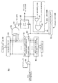
図2は、図1のDUTテスター6の概略を示す拡大したブロック図である。36個ものテスターがあるが、ここではそのうちの1つを説明する。図2を一目見れば明らかなように、概略ブロック図にしては相当な数の構成要素が描かれている。DUTテスター6に含まれるもので、このブロック図に描かれた要素の中には、機能的に非常に複雑であり、市販品としては入手できないものもある。ここで2つの点について明記しておく。第一に、図2の主要目的は、不揮発性メモリテストシステム1全体の重要な動作環境の基本特性を説明することである。図3以降の図に関連して詳細に説明する本発明は、図2について以下に説明する機構の拡張であるか、或いはその存在根拠を図2に見出すことが出来る新たな機構である。いずれにしても、この説明を書いている段階では読者がこれらの機構のどれに直面するかは明確にはわからない。現時点での目標は様々な好適な実施態様の多数の異なる詳細な説明の開始点として簡潔でありながら充分な情報を提供することにより、これらの実施態様の各々を簡明かつ適正に説明することである(異なる発明の各々について全てを開示する「長大な」明細書にならないように)。第二に、発展させた、すなわち拡張した実施態様の中には、図2に示す構成に大体においては一致するものの、その簡略化されたバージョンとは正確には「整合」しない情報を含むものもある。しかしこれは誤りや決定的な矛盾ではなく、全体像を完全な縮小版で表すように物事を簡略化して示すことが時に困難、或いは不可能な場合があるからである。この状況は地図と似ている。例えばコロラド州の標準サイズの道路地図では、州間高速自動車道I−70に乗って東へ向かえば、デンバーでI−25に入って北へ向かうことが出来ることがわかる。これは左折のように見える。実際、昔は左折であったが、現在は違う。このインターを詳しく記した地図を見ると、一連の部分的進路変更と割り込み車線が示されている。しかしながら標準サイズの道路地図が間違っていると言う者はいない。このレベルの抽象性においては正しいからである。同様に、図2は相当詳しく描かれているようではあるが、実際は中程度の抽象性で描かれた簡略図であり、一見「左折」に見える部分でも、実際は単純な「左折」とは言えない場合もある。
【0032】
図1に示したように、DUTテスタ6への主な入力は、対象とするDUTテスタ6のインスタンスに関連するテストサイトコントローラ4を起点としたテストサイトバス5のインスタンスである。テストサイトバス5は、テストサイトバス上のトラフィックをリングバス85又はVTバス89のトラフィックへと変換するマルチバスコントローラ88に結合している。更にリングバストラフィックをVTバストラフィックへと、そしてVTバストラフィックをリングバストラフィックへと変換することも出来る。図2に示したほぼ全ては、大規模集積回路の一部である。便宜上、1つのエンティティとして示してはいるが、タイミング/フォーマッティング及び比較回路52(以下に説明)は実際に8個のそのようなICである。各種外部DRAM(これらの一部も内部試験メモリ87の一部である。図3参照)を除いては、図2に示した構成要素の殆どは、APG(自動パターン発生器)と呼ばれる他の大型ICの一部である。リングバス85は、DUTテスタ6のAPG部における主要構成要素の設定や動作モードの設定等を行う為の汎用の機構間通信経路である。APGの各構成要素間には、様々な専用の広く高速な経路も存在する。VTバス89はDUTテスタ自体内で用いられる、IC間のバスである。
【0033】
リングバス85は、テストサイトコントローラがDUTテスタ6のAPG部と通信を行う為に使用する機構である。リングバス85は、マイクロコントローラシーケンサ19に結合しているが、このシーケンサは特殊用途向けマイクロプロセッサにたとえることができる。これは次アドレス計算機102が作成するアドレスを用いてプログラムメモリ中に記憶されたプログラムから命令をフェッチするものであるが、このプログラムメモリはマイクロコントローラシーケンサ19内部のもの(プログラムSRAM20)でも、外部のもの(外部DRAM21)でも良い。これらの2つのメモリは基本的に、論理的に共通の、プログラムカウンタ(又は命令フェッチアドレス)として作用するアドレス63によってアドレス指定されているかのように見え、また、いずれも実行すべきプログラムのソースになりうるものではあるが、(1)どの期間においてもいずれか一方のメモリしか命令フェッチメモリサイクルを実行せず、(2)実際、これらは電気的に異なる信号によってアドレス指定される、という点に留意すべきである。SRAMは高速であり、真のランダムアクセスが可能であるが、マイクロコントローラシーケンサ19(大型APG ICの一部)中の貴重な空間を使用する為、そのサイズは限られている。外部DRAMはかなりの容量に設定することが出来るが、線形的に実行しかつ分岐せずに連続した領域をアクセスするときのみ高速に動作することができる。SRAM20におけるプログラミングはアルゴリズム性の高いものが多いが、外部DRAM21は初期化ルーチンやランダム又は不規則データのようなアルゴリズム処理では容易に生成出来ないものに最も適している。
【0034】
次アドレス計算機102は、無条件ジャンプ命令又は条件ジャンプ命令、或いは各種プログラム制御フラグ25、その他のフラグ55及びマルチDUT処理用に供給される他の特定の信号(便宜上、DFE0:3 103及びDPE0:3104として別途示した)によって条件付けられた条件サブルーチン命令に応答して、実行中の試験プログラムに分岐を生じさせることが出来る。
【0035】
マイクロコントローラシーケンサ19がフェッチ及び実行する命令語は208ビットと、かなり長い。これは13個の16ビットフィールドから構成される。これらのフィールドはマイクロコントローラシーケンサ19本体の外部にある機構用にフェッチした命令情報を表すことが多い。このようなフィールドは、それらの関連する機構専用のものである。1セットのALU命令22が8個の16ビットALU24の集合へと印加され、他のセットはDUTテスタ内に分散する他の様々な機構に分配される。後者の状態は、「各種制御値及び命令」42と表示したライン及び文字で表している。
【0036】
8個の16ビットALU24は、各々それに関連する16ビット結果レジスタ(各ALUは他のレジスタも幾つか含んでいる)の周囲に構築された算術命令の従来のレパートリーを有する。結果レジスタの内3つと、それらが関連するALUは、X、Y及びZのアドレス成分27を生成する為のものであり、アドレス成分は様々に組み合わせられてDUTへと供給される完全なアドレスになる。8個のALU/レジスタ(DH及びDL)のうちの2つ以上は、32ビットデータパターン28をアルゴリズム的に作成するのを助けるものであり、32ビットデータパターン28は最大有効部分(DH)と最小有効部分(DL)に分割される。最後の3つのALU/レジスタ(A、B、C)はカウンタとして使用され、様々なプログラム制御フラグ25の生成に寄与する。これらのプログラム制御フラグは、プログラムで指定された繰り返し回数又は他の数的条件が完了した時点で実施されるプログラム制御及び分岐を補助するものである。これらのプログラム制御フラグ25はマイクロコントローラシーケンサ19へと返送され、マイクロプログラムされた実行機構を熟知する者には周知の方法で命令フェッチアドレスの値に作用することになる。更に各種の「他のフラグ」55も存在し、これらもプログラム分岐を行う為に用いることが出来る。これらはフェッチした命令語のそれぞれのフィールドによって制御されるDUTテスター6中の他の種々の機構から発生する。1つの特定の追加フラグとしてPD_ERR90を個別に明示的に示した。これは後デコード機構60を起点としてプログラムSRAM20へと送られるもので、後デコード機構60がエラーを発見したことを示すものである。このような追加フラグの他の例としては、VEC_FIFO_FULL26がある。より簡略化した他の図においては、これもその他のフラグ55に包含されている。これをここで個別に示したのは、マイクロコントローラシーケンサ19の動作の一側面の説明を助ける為である。
【0037】
VEC_FIFO_FULLの機能は、マイクロコントローラシーケンサ19によるプログラムの更なる実行を(一時的に)停止させることである。マイクロコントローラシーケンサ19がフェッチした命令と、DUTに印加すべき試験ベクターを最終的に送出する機構との間には多段のパイプラインが存在する。更に、DUTへの印加に向けて搬送されるときにベクターを伴うバゲージの一部は、最終的なベクター印加速度、或いは各ベクターの持続時間に関する情報である。従って、DUTへのベクター印加速度は一定である必要は無く、具体的には、あるベクター群の印加時間は、生成にかかった時間よりも長くても良い。マイクロコントローラシーケンサは、単純にプログラムをその最高速度で実行する。しかしながら、「ベクター消費」速度が「ベクター生成」速度と平均で等しくなければ、パイプラインにはほぼ無限の柔軟性を持たせなくてはならなくなることは明白である。以下に説明するアドレスマッパ29の出力にはベクターFIFO45があり、これがパイプライン中の柔軟な容量として作用する。信号VEC_FIFO_FULLは、パイプラインの先頭部(ヘッド)における新たなベクターの生成を一時的に中断することにより、パイプライン中の限界段数を超過しないようにするために使用される。
【0038】
更に説明を続けると、(3x16=48ビットの)X、Y及びZアドレス成分27がアドレスマッパ29に印加される。アドレスマッパ29の出力は、順序付けられた48ビットアドレス空間において、事前に選択されほぼ任意に再構成されたアドレス値である。この理解を助ける為に本題から離れるが、このアドレスマッパ29を、48ビットアドレス空間を完全に収容するメモリとし、各アドレスには48ビット値が保持されていると想定する(このようなメモリを現在実現しようとすれば大型冷蔵庫大となるであろうが、このことは一時的に無視して考える)。このようなメモリがあれば、どのようなアドレスが与えられても、他の任意に選択された、後に置き換えアドレスとして使用できる48ビット値へとマッピングすることが可能なルックアップテーブルを実現することができる。このようなアドレスマッピングが望まれる理由は、X、Y及びZアドレス成分が一般的に、特定のDUT内部構造のコンテキストにおいて、1つの大型リニアデコーダでは実現されにくい有用な意味を持つ為である。行、列、層、ブロック或いはページといった概念はテストエンジニアにとっては非常に便利なものであり、物理的に近い位置で生じた不具合は、それらのX、Y及びZアドレスにおいてこれに対応する近接性を持っている。試験結果におけるこのようなパターンは、何が悪いのかを評価し、欠陥部分の動作を予備部分の動作に分岐するために、一部分を、設計レベル、又は製造レベルで再プログラミングして修復する上で有用なものである。このような考え方からは、2つの問題が生じる。第一の問題は、48ビットを削減してDUTへと印加すべき実際のビット数(例えば32又は16)にすることである。この削減がどのように行われるかを簡単に説明すれば、これはXから何個かのビットを得、Yから何個かのビットを得、そしてZから残りのビットを得るということである。しかし全てではなく、いくつかのアドレスは、回路の他の部分の左右(又は左右及び上下)の鏡象である回路中に存在する可能性がある為、これが第二の問題となる。これには、連続するアドレス値が回路内において物理的な順序で並んでいる限り、ビットの意味が変わるという作用がある。このチップレイアウト特性は何回も生じ得るもので、ある1群のビット(例えばY)をどのように解釈するかは、それに付随する他(例えばZ)のビット値に依存する場合がある。アドレスマッパ29はX、Y及びZの生アドレスを「再パッケージング」することでこの種の状況を反映できるようにするために設けられたものであり、このような内部構造を有するメモリを試験する人々の便宜をはかるものである。実際にこれがどのように行われるかを説明する。アドレスマッパ29は、相互接続されたかなり多くの数のマルチプレクサ(MUX)から構成される。これは、説明の便宜上先に一時的に想定した、完全に収容されたメモリデコード方式における完全に任意のルックアップテーブル機能を実施することは出来ない。しかしながら、具体的には48ビットから実際に必要な数に削減する他の機構がある為、X、Y及びZアドレス成分のサブフィールドを必要に応じて並べ替えることが出来る。アドレスマッパ29は、制限された任意のマッピングを局所的な範囲において実施することが可能な、3個の16ビット(アドレス)ルックアップテーブルを更に有する。
【0039】
アドレスマッパ29のマッピングされたアドレス出力30は、アドレスとして各種バッファメモリ及び/又はTagRAM31A−B、そしてエラー捕捉RAM1/2(32A/B)へと印加される。これらのメモリは別個の機能を有してはいるが、集合的に内部試験メモリ87を構成する4つのメモリセット中の選択可能な区画として実現することが出来る。マッピングされたアドレス出力30は、また、アドレスビット選択回路37(その多重化機能は後に説明する)への1入力としても印加される。内部試験メモリは、異なる機能に使用される様々なRAMベースのメモリ構造を多数含むように構成することが出来る。これは異なるメモリセットの特定の部分を、関連する目的に使用することを宣言することにより実現される。図2に示されているのがこのような構成の1つであり、試験の進行に伴って構成を変えることが出来、このメモリセット用途に関わる処理全体は非常に動的であると考えられる。内部試験メモリ中に存在するいずれの部分(例えばエラー捕捉RAM32A−B)も、恒久的に固定されたハードウエアではない。不変なのは4つのメモリセットだけである。しかしながら、いずれの時点においても、(もし実際に定義されるとすれば)どのメモリセットのどの部分がエラー捕捉RAMであるかに関しては、現在確立されている構成に依存する。
【0040】
バッファメモリ31A及び31Bについて説明する。それらの機能は、DUTに印加することが可能なデータパターン33及びアドレス34を保持することである。これらは、実際には、それらの関連するバッファメモリからの別個の出力である。バッファメモリは「デュアルポートメモリ」ではないが、2つの異なるメモリセットの部分から構成されるのが望ましい。この場合、記憶済みデータ33が一方のメモリセットに保持され、記憶済みアドレス34が他方のメモリセットに保持されるようになっていることが望ましい。更に、バッファメモリへの書き込みを行う機構を明示していないが、これは1つには、実行されているプログラムの命令でテストサイトコントローラ4が起動するアドレス指定されたバスの動作により行うことができる。(図が非常に見にくくなる為に大部分を省いたが)リングバス85と呼ばれる「床下」の「ユティリティサービス」バスがあり、これが図2に示した要素のほぼ全てへと通じている。メモリセットへと情報を書き込む為の他のより高速な方法は、図3に関連して説明する。
【0041】
エラー捕捉RAM32A−Bはバッファメモリ31に印加されたのと同じアドレスによりアドレス指定される。これらは、エラーに関する情報の記憶及び取り出しを行うもので、その動作は後述する後デコード回路と連係して実施される。バッファメモリ31A−Bからの経路33、34と同様に、エラー捕捉RAM132Aからの経路62A〜Dは、リングバス(図示せず)によって配信される構成情報に基づいたメモリセット部分(エラー捕捉RAMとして動作するよう構成されている部分)からの多重化出力であることが望ましい。
【0042】
留意すべきは、データマルチプレクサ35はその入力としてALU集合24中のレジスタDH及びDLからのデータ28を受けると共にバッファメモリ31からの記憶済みデータ出力33をも受けるという点である。データマルチプレクサ35はこれらの入力(28、32)のうち、どちらをその出力38として提供するかについて、プログラムSRAM20中に記憶された値36に基づいて最初の選択を行う。その出力38は、以下に説明するような変更が加えられない限りは、2つのベクター構成要素のいずれか一方として(もう一方の構成要素はアドレスビット選択回路37の出力39である)送信ベクターマッパ/シリアライザ/受信ベクター比較データ回路40へと印加される。
【0043】
回路40は3つのベクター関連機能を実行することが出来る。すなわち、ベクター構成要素(38、39)を組み合わせてDUTに印加(伝送)するベクター全体を順序付けられた論理表現にすること、送信ベクターの論理表現の順序付けられたビットと、信号(ベクター中のそのビット)を届ける為にDUTに接触するピン電子回路(例えばプローブ先端等)の実際の物理チャネル番号との間に動的な任意の対応付け(マッピング)を実施すること、そしてそれを受け入れるDUTに対し、別個に、順に(連続的に)印加されるように全体の論理ベクターを部分に分割する際にコンパイラと連係して作用することである。これらの機能のうち、どれを実行するかは、SRAM41からの制御信号により決定されるが、この制御信号もまた、マイクロコントローラシーケンサ19によりフェッチされた208ビット命令中の1フィールドに従ってアドレス指定される。
【0044】
更に回路40に含まれているのは、DUTディスエーブル(DUT禁止)論理部90である。これが存在する理由は、最高4つのDUTのうち、1つ以上のどのDUTを無効(ディスエーブル)にするのかを表示する、ある程度静的で、ある程度試験結果により変わるが、全てプログラム的に規定される様々な状況に対応する為である。これらの表示は、4つの信号DD0:3 44b(DUT0、DUT1等に対するDUTディスエーブル)により伝達される。これは1つのテストサイトでのマルチDUTテストをサポートするものであり、この詳細は組み込んだ関連特許出願に記載されている。回路40の出力は最高64ビットまでのベクター44aであり、DUTディスエーブル信号44bと共に、ベクターFIFO45へと印加される。FIFO45は、完全に埋まると信号VEC_FIFO_FULL26を生成するが、この信号の意味及び用途は先に説明した。期間発生器49(後に触れる)からの信号VEC_FIFO_UNLOAD47を受けとると、ベクターFIFO45の最上部にあるベクターがそこから取り出される。取り出されたベクター46は、関連するピン電子回路9を介してDUTに接続するタイミング/フォーマッティング及び比較回路52に印加される。即ち、(種々のテストサイト内の)ピン電子回路9の各々が、送信及び受信ベクター7及びピン電子回路構成情報8を、関連するタイミング/フォーマッティング及び比較回路52から受信する。
【0045】
タイミング/フォーマッティング及び比較回路52は、構成及び制御情報を受信する為にVTバス89に接続している。先にも説明したように、タイミング/フォーマッティング及び比較回路52は実際には8つのICであるが、本明細書においては、便宜上1つのエンティティとして取り扱うものとする。
【0046】
タイミング/フォーマッティング及び比較回路52は、マイクロコントローラシーケンサ19のプログラムSRAM20と同じ命令アドレス(小円で囲まれたA)によりアドレス指定される内部SRAM54を有する(外部DRAM53を内部SRAM54の代わりに使用しても良いが、これは図示していない増分カウンタにより局所的にアドレス指定される)。内部SRAM54(又は外部DRAM53)は、関連するフォーマットを有するドライブサイクル及び比較サイクルの生成を助けるものである。ドライブサイクルは、RAMの54又は53の一方から供給される事前に選択されたフォーマットを使って送信ベクターをDUTへと印加するものである。比較サイクルはDUTから供給されるベクターを受信して検査し、先に供給された比較データと一致するかどうかを判別するもので、この試験もまた、RAMから供給される事前選択されたフォーマットに基づいて行われる。ドライブサイクル及び比較サイクルはいずれも、その持続時間に関して調整可能であり、負荷を印加するかどうか、そして何時印加するのか、何時データをラッチ又はストローブするのか、信号がReturn−To−Zeroであるのかないのか、被駆動信号をその補完信号で囲むのかどうか等について適切に調整可能である(これらのオプションが上述した様々なフォーマットである)。
【0047】
タイミング/フォーマッティング及び比較回路52によって生成される比較結果には、論理値が誤りだったためにそのチャネルが不良となったのか(機能エラー)、及び/又はその電気特性が許容範囲を超えていた為に不良となったのか(パラメータエラー)について、チャネル毎の情報を含んでいる。更に、組み込んだ特許出願に記載されているように、複数のDUT試験が実施される場合、どのチャネルがどのDUTに関連しているのかは既知である。これにより、4つの信号DFE0:3(いずれの番号のDUTの機能エラー)103及び4つの信号DPE0:3(いずれの番号のDUTのパラメータエラー)104の生成が可能となる。
【0048】
タイミング/フォーマッティング及び比較回路52により実施される比較処理でも64ビット値が生成され、これが、回路40の論理的反転機能を有すると考えることが出来る受信ベクター逆マッパ/デシリアライザ57へと供給される。(回路57の動作はSRAM58により制御されるが、これは回路40のSRAM41による制御に対応する)。そして回路57の出力59は後デコード回路60及びエラー捕捉RAM1 32Aへと印加される。後デコード回路60は入力エラー情報59と、エラー捕捉RAM1 32Aに以前に記憶されたエラー情報の両方をプログラム的基準に基づいて検分し、凝縮した、より容易に解釈出来るエラー情報を生成することが出来る。この生成したエラー情報は経路61を介して他のエラー捕捉RAM2 32Bに記憶しておくことが出来る。一例として、特定のアドレス範囲でエラーが生じた回数の計数値を作成すること等があげられるが、このような情報はいつ代替回路を起動してオンチップ修復を試みるかを決定する上で有用である。
【0049】
次に期間発生器49及びこれに関連するタイミングSRAM51について説明する。これらは8ビット信号T_SEL43に応答して、マイクロコントローラシーケンサ19によりフェッチされた208ビット命令の各々について、タイミング/フォーマッティング及び比較回路52の関連する動作の継続時間を決定する。T_SEL43は、フェッチされた命令中の異なるフィールドによって表される各種制御値及び命令42の要素である。この信号は、8ビット値なので、256の異なる「事象」を表す、即ち符号化することが出来る。この場合、これらの「事象」は、タイミングSRAM51に記憶され、T_SELによりアドレス指定される28ビット値である。アドレス指定された28ビット値23の各々は19.5ピコセカンドの分解能で所望の継続時間を指定するものである。アクセスされた28ビット継続時間値23のシーケンスは期間FIFO50中に記憶され、そのシーケンスの個々の要素が取り出されて、それらの意図した対応ベクター(このベクターは、ベクターFIFO45に記憶される)の取り出しに同期して印加されるようになっている。
【0050】
FIFO50の最も古いエントリ中にある粗タイミング値フィールドは5ナノセカンドの分解能で継続時間情報を含んでおり、この情報から、次の送信ベクターを、ベクターFIFO45からタイミング/フォーマッティング及び比較回路52に送る信号VEC_FIFO_UNLOAD47が生成される。随伴信号TIMING REMAINDER48もまた、回路52へと印加される。ここで19.5ピコセカンドという最終分解能に達する。
【0051】
次に図3を参照するが、これは図2のブロック図に示した内部試験メモリ87の概略ブロック図64である。メモリ87は、アドレスマッパ29から、種々のアドレス選別部77、78、79へと印加される48ビットのマッピング済みアドレス30を受ける。アドレス選別部はメモリセット73〜76に関連付けられている。これらのメモリセットの各々は、例えばECR32等の種々の機能を個別に実施することが出来る完全なメモリ機構である。これらのメモリセットのうちの2つ(73、74)は外部DRAMに属し、他の2つは内部SRAMに属している。2つの外部DRAMメモリセットは常に同じアドレス選別機能を実行するもので、従って同じアドレス選別部77を共用している。一方、内部SRAMメモリセット75、76は、それら自体に関連付けられたアドレス選別部78、79をそれぞれ有する。これらのアドレス選別部は、アドレスを変えずにそのまま、或いは変更したアドレスを出力することができるが、そのやり方については、組み込んだ特許出願の1つにある程度詳細に記載されている。
【0052】
各メモリセットはメモリセットコントローラを備えている。外部DRAMメモリセット73、74はDRAMメモリセットコントローラ65、66をそれぞれ含み、内部SRAMメモリセット75、76はSRAMメモリセットコントローラ67、68をそれぞれ含む。DUTの試験中、これらメモリセットのいずれかに向けられたメモリトランザクション用アドレスは、それぞれに関連するアドレス選別部から関連するメモリセットコントローラに到達する。4つのメモリセットは全て、基本的には内部試験メモリへと入る従来の経路(後デコード回路60をバイパスする経路)である経路59を介してデータを直接受信することが出来る。DUTの試験中は、後デコード回路60から供給され、エラー捕捉RAM232Bへと書き込まれることになるエラーデータ61は、メモリセット2及び3にそれぞれ関連しているデータ選別部82〜83へと最初に印加される。データ選別部80〜83は、それらがどのように構成されているか、及び、それらが実行する機能に応じて、供給されるデータに変更を加える場合もあれば加えない場合もある。アドレス及びデータ選別部はそれぞれアドレス及びデータの高速経路であり、これらは必要とされる最高速度で動作するよう意図されている。リングバス(ここでは図示していない)が、他の手法でアドレス及びデータをメモリセットに搬送することについても後で手短に説明する。
【0053】
この時点において、各々に(選別された)アドレス及び(選別された)データが入力される4つのメモリセットコントローラ65〜68がある。これらのメモリセットコントローラの各々は、対応するメモリに結合している。即ち、DRAMメモリセットコントローラ73及び74はそれぞれ、外部DRAM69及び70に結合しており、SRAMメモリセットコントローラ75及び76はそれぞれ、内部SRAM71及び72に結合している。これらの構成が4つのメモリセット73〜76を形成しており、これらのうちの2つ(75、76)は、容量が比較的少ない高速SRAMを有し、他の2つ(73、74)は、大容量のより遅いDRAMを有している。ここで重要な点は、DRAMメモリセットをどのようにしてSRAMメモリセットと等しい速さにするか、そしてユーザーの嗜好や試験プログラム方針に応じて、DRAMのいくつかの代替構成をどのようにして組み込むかである。従って、DRAMメモリセットコントローラ65、66は、構成可能であり、異なる種類のメモリトランザクションを実施するものでなければならず、より単純なSRAMメモリセットコントローラ67、68と全く同じ構成というわけにはいかない、ということがわかる。図を簡潔にする為に図3にはこの柔軟性を提供する構造を示していない。ここでは、各メモリセットコントローラに特定の動作モード及び所望の構成において指示を行うリングバス(ここでは図示していない)に、各メモリセットコントローラが接続されていると言うに留める。これらのモードの一部はデータの記憶方式に関わるものであり、他の一部はデータの再取得に関わるものである。結論として、各メモリセットは対応するデータ出力(62A〜D)を有し、これらは後の処理の為に後デコード機構60に送られる、ということに留意されたい。更に、メモリセット0及び2からのデータ出力は、マルチプレクサ(以下、マルチプレクサをMUXとも記す)84へと印加され、その出力がデータマルチプレクサ35へと送られる記憶済みデータ33となる点にも留意されたい。同様に、メモリセット1及び3からのデータ出力はマルチプレクサ127へと印加され、その出力がアドレスビット選択マルチプレクサ37へと送られる記憶済みアドレスとなる。マルチプレクサ84及び86の存在理由及びこれらがどのように制御されるのかについての詳細は本願においては重要ではない。これらについては、組み込んだ特許出願に記載されている。
【0054】
次に図2に示した後デコード回路60の概略ブロック図91である図4A及び図4Bを参照する。図4Aには、図2に示すものと同様に、後デコード機構60への入力として機能する2つのデータ経路が示されている。これらの一方は受信ベクター逆マッパ/デシリアライザ57からの単一ソース59であり、他方はECR(ECRを、これまで、エラー捕捉RAM1 32A、または、ECR1として示してきた)として動作するように構成されたメモリセットのいずれか1つに対する内部テストメモリ87からの4つのソース62A〜Dである。4つのソース62A〜Dについては、いずれのメモリセットにおいても、一度には1つの(アクティブな)ECRしか存在しない。5つのソース全てがマルチプレクサ94へと入力されるが、マルチプレクサ94はその中の1つを、種々の入力マスク96、97、105、107へと、及び、マルチプレクサ94の出力とこれら種々の入力マスクの出力との間で選択を行うマルチプレクサ108へと印加すべき入力として、選択する。
【0055】
本願においては、「マスク」という語を、データフィールド内の選択したビットを何らかの配慮に基づいて排除又は包含する為のパターン及びそれに関連する機構を指す語として従来通りに使用している。マスクパターンは対象とするデータフィールドと同じ数のビットを有しており、データフィールドビットと一対一で対応しているものと考えられる。本願で使用するマスクは、無視すべき位置、即ち考慮対象から「マスクアウト」すべき位置に1を有している。データフィールドは、不良を0で表すという慣例に従う。通常、考慮対象は、マスク適用後のデータフィールド中にある0の存在、又はその数である。実際にマスク機能を実施する回路は後で説明する。現時点では、図4A及び図4Bの一般的な性質を検討するので、マスク処理をブロック図レベルで単純に取り扱うものとする。入力マスクのブロック図レベルにおける性質とは、マスクアウトすべきビット位置に1を設定して、その位置が不良表示に影響することがないようにするものである。
【0056】
続いてジャムマスクレジスタ93について説明するが、これは32ビットのマスク値を受ける為にリングバス85に結合している。このマスク値は入力マスク96へと供給される一方で、そのビット毎の補数がインバータ98の処理により入力マスク97へと供給される。これらのマスクは所与のパターンの持続時間中は一定である。即ち、あるデータ値から次のデータ値へと、ルーチン的に変化することは想定されていないということである。入力マスク自体は入力データとして、マルチプレクサ94がPD制御レジスタ92(これもリングバス85に接続している)からの信号ERR_DATA_SELに基づいて選択したソースを受信するものである。入力マスク96、97の出力は、追加入力としてマルチプレクサ108へと供給される。
【0057】
マルチプレクサ108は更に2つのマスクされた入力を受ける。これらは入力マスク105及び107(これらへの入力もまた、マルチプレクサ94の出力であり、これらのマスクもまた、インバータ106によって処理された補数である)の出力である。しかしながらこの場合のマスク値のソースは、マルチプレクサ95及びマルチプレクサ制御信号BM_SELにより選択されたバッファメモリであることが予想される。この為に、マルチプレクサ95は、入力として4つのソース62A〜Dを有するということに留意されたい。この構成によれば、パターンが実施されているときに、入力マスク105及び107により使用されるマスクをサイクル毎に変化させることが出来る。
【0058】
明らかなように、マルチプレクサ108への入力として提供されるのは、アドレス指定されたデータに様々なマスクをかけたもの4つと、アドレス指定されたデータにマスクをかけていないもの1つである。マルチプレクサ108がこれら5つのデータからどれを選択し、マスクされたデータ114として送出するのかは、マルチプレクサ制御信号PD_MASK_MODEにより決まる。
【0059】
これまでに述べた3つのマルチプレクサ制御信号(ERR_DAT_SEL、BM_SEL、PD_MASK_MODE)及び後に説明するもう1つの信号(PD_ERR_SEL)は、全て、リングバス85を介してPD制御レジスタ92に送られるトラフィックによりその内容がどのように設定されるかに従って、PD制御レジスタ92からの出力として生成される。
【0060】
次に図4Bを参照する。この図はどちらかというと込み入った図のようであるが、見た目程複雑ではない。左側上隅の部分について説明する。ここには解析マスク及び解析カウンタ機構が32個示されている。これらがどのような機構であるかを説明する。
【0061】
まず、このブロック図レベルにおいて、解析マスク(ANYL.MASK_0・・・ANYL.MASK_31、110a〜z)は、マスクされていないデータビットの1つ以上が0であった場合に0で表示し、マスクされていないビット中に不良表示(0)が全くなかった場合に1を表示する一ビット出力を生成するという特性を有する。各マスク回路110a〜zにより使用されるマスクは、関連するMASK_0・・・MASK_31レジスタ109а〜zにより供給されるが、これらのレジスタはその値を受ける為にリングバスに接続している。ここで留意すべきは2つの点である。第一には、解析マスク回路110a〜zの出力が対応する解析カウンタ(ANYL.CNTR_0・・・ANYL.CNTR_31、112a〜z)へと送られるという点である。これらのカウンタはそこに送られた0の数を計数し、それに関連するマスクにより(例えばパターン中で)エラーが発見された回数の合計を得る為に使用することができる。第二には、32のマスク出力全てがその組113内に集められ、それらを(経路61を介して)ECRに記憶するか、或いはPDエラーマスク120によって更に解析することができるという点である。
【0062】
更に説明を続けると、解析カウンタ112a〜zは以下のブロック図レベルの特性を有している。これらは、対応するロードレジスタ(CNTR_0 LOAD REG.・・・CNTR_31 LOAD REG.,111a〜z)中に記憶された内容によって与えられた、事前にロードされた値からカウントダウンを行うものである。ロードレジスタに記憶される内容は全て、リングバスを介してそれらに個別に送られるトラフィックにより別々に設定される。これにより、カウンタを、カウントダウンを開始する閾値に事前に設定することが出来る。これらがゼロまで計数すると、対応するカウント終了フラグ(TCF_0,・・・TCF_31、115a〜z)は0を表示し、それ以上のカウントダウンが禁止される(カウンタは0で止まる)。これらは、信号LOAD_COUNTERS(この信号が生じると、常にリロードが強制される)の作用により閾値がリロードされるまで0のまま留まる。また、QUALIFIED_LOADという信号もあるが、これはカウンタが未だ0に到達していない場合にそれぞれのレジスタ111a〜zからカウンタ112a〜zの各々へリロードを行うものであり、この場合は個別のリロードは禁止される。
【0063】
カウント終了フラグ115a〜zは、集合116として集められて、解析マスク110a〜zからの集合113との交互入力としてマルチプレクサ118に供給されるということに留意されたい。集合116、113はまた、マルチプレクサ117にも供給されるが、ここから、それらから選択されたうちの1つを、経路61を介してバッファメモリに格納することができる。マルチプレクサ117及び118の両方における選択は、PD制御レジスタ92から送られる制御信号PD_ERR_SELにより決定される。
【0064】
次に図4Bの他の部分を説明するが、前述した解析マスク及び解析カウンタ機構により、事前選択した閾値を超える計数値に関して生成された表示を用いて、様々なエラー状況を検出し計数することが可能であることが理解されよう。出力113及び116に存在する事象の状態を、マルチプレクサ117及び経路61を介してメモリ中に記憶することが出来る。同じ状態の事象は、マルチプレクサ118及びPDエラーマスク120(入力型のマスクであり、そのマスクはリングバスにより設定されるエラーマスクレジスタ(ERROR MASK REG.)119の内容に含まれる)を介して更なる解析を受けることも可能である。PDエラーマスク(PD ERROR MASK)120からの32ビット出力121は、NANDゲート122へと供給され、そこで他の2つの「0がエラーである信号」(ゲート129及び136の出力)と論理和演算される。これら後者の信号については後で説明する。従って、このように得られた論理和は、1が表明された信号を意味する信号PD_ERR90として生成され、マイクロコントローラシーケンサ119に供給される。
【0065】
マスクされたデータ114は更に図4Bの下部に示した他の2つのマスク/カウンタ構造にも供給される。まず、ACCUM.ANYL.MASK123(そのマスクはリングバスにより設定されるACCUM.MASK REG.124に含まれる)について説明する。これはマスク110a〜zと同様に動作する。その出力もまた、マスク123により0が提供されたときにカウントダウンを開始し、信号LOAD_ACCUM_CNTRが作用したときにACCUM.LOAD REG.125により閾値に事前設定されるACCUM.CNTR.126に供給される。レジスタ125中の閾値は、リングバスにより供給される。カウンタ126の出力は、0までカウントダウンすることが出来、また、0までカウントダウンすると、カウント終了フラグTCF_ACCUM127が0を表明し、カウンタ自体はリセットされるまで0のまま留まる。この時点に至るまでは要素123〜127の構造は、解析マスク及び解析カウンタに関連して先に説明したものと本質的に同一である。相違点は、結果をどのように出力することが出来るか、及び、意図するマスクが何かについてである。要素123〜127の目的は、エラーを含むワード全体の数を累積し、これを所望の閾値と比較することである。説明を先に進めると、要素127からの信号TCF_ACCUMは、1ビットラッチA_Latch128及びORゲート129から成る1ビットマスクに供給される。ORゲート129の出力は、閾値に一致した場合は、0が故障を検出したことを意味する論理で表示を行うが、この出力は、PD_ERR90の生成におけるもう1つの入力である。
【0066】
図4Bには更にもう1つのマスク及び累積機構が示されている。BITWISE ANYL.MASK130、BITWISE MASK REG.131及びBITWISE LOAD REG.132は、先に説明した、これらに明らかに対応する要素(例えば123〜125)と同じである。唯一の相違点は、レジスタ132へのロード信号が、その独自の信号LOAD_BITWISE_ACCUMであるという点である。ブロック図レベルの特性において生じる相違点は、ラッチBITWISE ACCUM.133が他のカウンタのような単なるカウンタではないという点である。要素133は、マスク処理後に、到達する各マスク結果中の0の数を計数し、これをレジスタ132中の初期の閾値から減分する数量として累積する。閾値が0まで減分されると、ラッチ134のフラグTCF_BITWは低(ロー)を表明する。前述と同様のことが、B_LATCH135及びORゲート136から成る1ビットマスクにより再び開始され、この1ビットマスクの出力は、NANDゲート122によるPD_ERR90の生成に寄与する最後の要素となる。
【0067】
後デコード機構60の概要の説明の最後に、図4Bの上部右隅に位置する4ビット書き込み専用レジスタ137の機能について簡単に説明する。これはリングバスにより設定されるもので、その出力ビットの1つがクロックに同期してTrue(1:真値)として出力されたときに、それに関連する名称の制御信号としてそれ自体を表明するものである。これらは上記の説明において既に触れた信号であり、上述したカウンタにより使用される各種LOAD信号である。これらのLOAD信号が残留しつづけると機能障害が生じる可能性がある為、それらの信号は、所定の機能を果たした後消滅するように設定されている。この為には、ORゲート130はこれらのLOAD信号のうち1つ以上がTrueであることを検出し、これをANDゲート139へと供給し、次のクロックサイクルが生じたときに、レジスタ137の内容を全て0にリセットする。これはワンショットタイプの機構である。
【0068】
最後に、これまでに参照した図には示していないが(図7において図示)、各種カウンタ中の値は、リングバス上に読み出すことが出来る。
【0069】
次に図5を参照する。図5は、各種マスクがどのように機能するかを示すブロック図165である。入力マスクは32ビットの入力データ値166と、32ビットのマスク値167とからなる。マスク値167はレジスタから得るようにしても(静的方式の場合)、或いはメモリからマスクデータを読み出す等、より一時的な方法で得るようにしても良い。いずれにしても、2つの要素166と167の間には、ゲート168a〜zによるビット毎の論理和演算が実施される。この結果得られた32ビット数値169が入力マスクに対する出力となる。解析マスクについては、数値169がANDゲート170へと供給され、ANDゲート170は、数値169のいずれかのビットが0であった場合にその出力として0を生成する。
【0070】
ビット毎累積機構(BITWISE ACCUM.)133の性質を理解する為に、この回路のブロック図140である図6を参照する。これは、マスクレジスタ(BITWISE MASK REGISTER)141を含んでおり、このレジスタの32ビット値142は32ビットの入力データ値143とビット毎にNOR演算される。この時点における図5のマスク構成との相違点は、ゲート144a〜zがORゲートではなく、NORゲートであるという点である。この違いの結果、マスク処理後に残った不良に対して生成されるのは、0ではなく1ということになる。これは、このようになっていれば不良表示の発生数の和を取って総数を得ることがより容易な為である。これらはNORゲートをグループ化して対とし、これらのNORゲート対の出力を加算器145a〜oに供給することにより加算される。加算器145a〜oはそれら自体も対を構成しており、それらの出力は更に他の加算器146a〜hにさらに供給される。この方法によれば、入力値143中の0の総数は、加算器147の出力に出力されるまで個別に累積されることになる。そしてこの出力は、BITWISE LOADレジスタ(BITWISE LOAD REG.)132内の閾値から開始される値を減分するために利用される。この閾値は、マルチプレクサ150へのマルチプレクサ制御信号LOAD_BITWISE_ACCUMの最初の表明によって、BITWISE ACCUM.レジスタ151に入れられたものである。これはレジスタ151中の値が加算器147の出力により減分されるように設定される。これは減算回路148により実施され、その後その出力はマルチプレクサ150を通過してレジスタ151中に記憶される次の値となる。この結果、レジスタ151は、加算器147が生成した和によりカウントダウンされることになる。レジスタ151が0を過ぎると、カウント終了フラグ機構134が0を表明する。
【0071】
図7は上述した解析及び累積カウンタ156の性質を説明する為のブロック図154である。解析カウンタ及びそれらのロードレジスタ157は24ビットであるが、累積用のものは32ビットである。いずれの場合も、マスクから計数される0はNORゲート158へと供給されるが、このNORゲート158に対する他の入力は信号YES_ZERO164である。YES_ZEROは、カウンタ156の(True:真値)出力により駆動され、カウンタ156の内容が0のときには常にYES_ZERO=ONE(1)を生成する機能を有するNORゲート159により生成される。YES_ZEROは2つの役割を持つ。第一には、マスクからの入力にかかわらず、NORゲート158の出力を強制的に0とすることにより更なる計数を禁止することである。カウンタ156は、実際には1を計数するので、計数はされないことになる。第二には、TCFラッチ160を設定することであり、これによりそのNOT−Q出力は0となる。
【0072】
解析カウンタについては、0となるTCF信号はANDゲート161を通じて作用し、信号QUALIFIED_LOADの作用を禁止する。これにより、前述したようにレジスタ156のリロードが阻止される。QUALIFIED_LOADが禁止されない場合、これはORゲート162を通過し、ここでQUALIFIED_LOADもしくはLOAD_COUNTERSによりカウンタ156がレジスタ157中の値でロードされ、更にTCFラッチ160がリセットされることになる。これは点線171中の回路で示されている。
【0073】
累積カウンタについては、点線171内の要素が点線172中に示される単純な構成に置き換えられる。この場合、直接的にカウンタ156をロードし、TCFラッチ160をリセットする為に信号LOAD_ACCUM_CNTRが印加される。
【0074】
カウンタ156の出力はバスインターフェース155に供給されということに留意されたい。その値は、このバスインターフェースからリングバス上に送ることができる。
【0075】
まとめとして、後デコード機構にとって望ましい特徴を幾つか述べる。ここでは、図4A、図4B、図5、図6及び図7の主要構成をどのように利用して所望の目的を達成することができるかについて簡単に説明する。改良型後デコード機構の「オンザフライ解析」機能は、経路59がマルチプレクサ94に接続していることにより実現される。これにより試験結果を内部試験メモリ中に事前記憶する必要なく解析を続行することが可能となる。
【0076】
オンザフライで解析を行う能力と、アドレス毎に変えることが出来るマスクとしてバッファメモリの内容を使用することができる能力とが結びつくことにより、新たに生じたエラーだけを認識することが出来る機能が助長される。これを「増分的後デコード解析」と呼ぶものとする。これは、ECR内のエラーデータを先の試験中に得て、そのエラーデータをバッファメモリへとコピーし、その後そのバッファメモリをマスクとして使用することで新たな試験中は古いエラーを隠し、新たなエラーだけを識別して更なる処理を実施できるようにするというものである。この機能は経路62A〜Dがマルチプレクサ95に結合することでサポートされている。これはまた、入力マスク105に結合したインバータ106によってもサポートされている。これは、これらのインバータが、「0は不良を表示する」というフォーマットを、マスクにより隠されるビット位置を示す論理1に反転することができるからである。しかしながら最初の試験においては、その試験の第一のパスをマスクなしで捕捉できるようにする為に、入力マスク96及びマルチプレクサ94と共に、ジャムマスクレジスタ93中に全0のマスクを使用することが望ましい。その後、マルチプレクサ94の代わりにマルチプレクサ95を使用して増分型処理モードを開始することが出来る。
【0077】
上述した増分的分析機構はECRからバッファメモリへのコピー能力に依存するものである。内部試験メモリであるメモリシステム自体は、そのようなコピー処理を実現する手段を持たない。しかしながら、この処理は上述した改良型後デコード機構の助けを借りれば可能である。具体的に言えば、経路62A〜Dのいずれかを起点とし、経路61を終点とする無変更データの伝送用経路が存在する。この無変更経路はマルチプレクサ94から始まり、そこからマルチプレクサ108へと入り、適正な解析マスク110a〜z構成を通過し、経路113に沿ってマルチプレクサ117にて終わる。適正な解析マスク110a〜z構成とは、各々が、そのマスク番号に対応するビット位置(この位置においては0)以外の位置において全て1であるマスクを有するというものである(この一見奇異とも思われる条件は、各解析マスクが、単一ビットしか出力せず、及び、データを変化させることなく通過させるように複数のこれらのマスクを構成するいう事実によるものである)。
【0078】
改良型後デコード機構60によれば、いくつかの場合には、同時解析をおこなうことができる。例えば、各累積解析機構123〜129及びビット毎解析機構130〜136が別々にそれらのタスクを実施するのと同時に、解析マスク110a〜zの集合は、そのタスクを実行することが出来る。これが可能であるのは、これらの機構の各々が、別々に、そして同時にそのデータ114にさらされる為である。
【0079】
累積解析機構123〜129が経路114上に出現するデータワード中に差別化されていないエラーの存在又は不在に関して(すなわち、データワード内のエラーが複数あるかないかを区別することなく)作用するものであることが理解されよう。即ち、データワード中の1つ以上のエラーの存在は、単一のエラーと同じように取り扱われるのである。対照的に、ビット解析機構130〜136は経路114上に現れるデータワード中の実際のエラーの数に応答する。
【0080】
最後に留意すべきは、カウント終了フラグの集合値116がマルチプレクサ117へと印加され、これをマルチプレクサ117から経路61を介してバッファメモリへと記録することが出来るという点である。以下は、この機能が有用である理由を示す例である。ECRがZ(すなわち、Zブロックの)TagRAMとして動作するように構成されていると想定する。各ブロックに関連するエラーに毎に個々の閾値を設けることが望ましい。これを行うには、各ブロックアドレスに対するカウント終了フラグをECRに記録し、その後ブロック間の解析カウンタをリセットする。記録された情報は、それぞれの閾値を超えたブロックを示すことになる。
【0081】
以下においては、本発明の種々の構成要件の組み合わせからなる例示的な実施態様を示す。
1.被験メモリ(14)の試験結果をメモリテスタ(1)で解析する方法であって、
(a)被験メモリに試験処理を実施して結果データ(56)を生成するステップと、
(b)作業位置に前記結果データを前もって記憶することなく、前記結果データにマスク(96,97,105,110,120,167,170)を適用するステップと、
(c)前記マスクの適用後に、前記結果データ中に残るエラー表示に従ってカウンタ(112)を起動するステップ
からなる、方法。
2.前記カウンタの内容を閾値(151/157)と比較し(148/156)、閾値を満たしたときにエラー信号を生成するステップを更に含む、上項1の方法。
【0082】
本願の概要は以下の様である。後デコード機構(60)へのデータ経路を変更することにより、後デコードは、データが内部テストメモリ(87)内の宛先メモリ構造(32A)に配置される前または配置されるときに、そのデータを処理することが可能になる。他のデータは、後デコード機構に供給される前に、まず内部テストメモリ内のメモリ構造に依然として配置される。広範なマスキング機能(96,97,105,107,110,120,167,170)をエラーテーブルのコピー機能と組み合わせることにより、新しいテストに対して増分式後デコード解析を可能にすると共に、以前のテスト中に不良として既にわかっている位置におけるエラーをカウントすることを回避する。ワード内のエラーとビットエラーの両方を累算することができる。後デコード機構は、しばしば、データがオンザフライで供給されるか、内部テストメモリ内の構造から供給されるかに関係なく、データを一回調べることにより複数のタイプの結果を生成することができる。後デコード機構は、エラーのアクティビティに関するものを決定するための閾値を表す予めロードされた値からカウントダウンを行うカウンタ(112)を備えている。カウントが0になるとカウント終了フラグ(160)が生成される。種々のカウント終了フラグの値が、データを内部テストメモリに記録するときにいつでも使用できる。カウンタには、しばしば、1つのテスト段階の終了時及び次の段階の準備の際に、初期カウント値(111)がリロードされる。カウンタが各初期値レジスタを有し、単一コマンドを受信したときにそれらのレジスタがカウンタにリロードすることができるように、カウントを構成することによって、オーバーヘッドのいくつかを削減し、有用性を増すことができる。カウンタに対してカウント終了フラグを提示することにより、カウンタがその初期値レジスタからリロードしないようにすることができる(161)。
【0083】
【発明の効果】
本発明の改良された後デコード機構によれば、メモリシステムの試験に関するオーバーヘッドを削減することができるので、試験時間を短縮することが可能となる。
【図面の簡単な説明】
【図1】本発明に従って構成された、広範囲に再構成可能な不揮発性メモリテスタの略ブロック図である。
【図2】図1のDUTテスタ6を拡大して示した略ブロック図である。
【図3】図2のブロック図に示した内部試験メモリ機構の機能ブロックの略図である。
【図4A】図2に示した後デコード機構60の略ブロック図である。
【図4B】図2に示した後デコード機構60の略ブロック図である。
【図5】図4のブロック図中に用いたマスク回路のブロック図である。
【図6】図4のブロック図中に用いたマスク及びビットワイズカウンタ回路のブロック図である。
【図7】図4Bに用いた特定のカウンタ及びカウント終了フラグ回路の略ブロック図である。
【符号の説明】
1 メモリテスタ
14 被験メモリ
56 結果データ
96、97、105、110、120、167、170 マスク
112 カウンタ[0001]
BACKGROUND OF THE INVENTION
(Related patent applications)
The subject of this application is a US patent application filed on September 28, 2000 entitled “MEMORY TESTER HAS MEMORY SETS CONFIGURABLE FOR USE AS ERROR CATCH RAM, TAG RAM's, BUFFER MEMORIES AND STIMULUS LOG RAM”. ). This US patent application discloses an operation mode of address selection and data selection targeted by the present application. For this reason, this US application is incorporated herein by reference.
Further, the above US application itself was filed on September 20, 2000, and incorporated US patent application No. 09 / 665,892 entitled “ERROR CATCH RAM FOR MEMORY TESTER HAS MEMORY SETS CONFIGURABLE FOR SIZE AND SPEED”. It is. This latter application describes in detail the memory system used in the preferred embodiment described below, which is not necessarily essential to the present application, but is a currently recommended system. It is difficult to explain the present disclosure without its attributes, so US patent application Ser. No. 09 / 665,892 is also incorporated herein by reference.
[0002]
[Prior art]
The penetration of electronic devices and their functions in everyday life is extremely significant. Many people use personal computers at home and carry multiple productive tools for a variety of miscellaneous purposes. Many personal productive electronic devices include some form of non-volatile memory. The mobile phone uses a non-volatile memory so that the phone number and settings programmed by the user can be retained even when the power is turned off. In the case of a PCMCIA card, a non-volatile memory is used so that information can be maintained even when the PCMCIA card is removed from the computer slot. Many other common electronic devices similarly utilize the long-term storage capability of non-volatile memory in assemblies that are not powered.
[0003]
Non-volatile memory manufacturers who sell non-volatile memory to electronic device manufacturers must use a tester to check whether the memory manufactured in-house operates properly. Since nonvolatile memories are manufactured and sold in large quantities at a consistently low cost, it is very important that the time required for testing individual products is as short as possible. Non-volatile memory buyers want to require minimal testing or no testing to save costs when incorporating purchased memory devices into higher cost assemblies, so memory manufacturers A high shipping yield is required. Therefore, the memory test procedure must provide a sufficiently high efficiency so that the majority of nonconforming items, preferably all nonconforming items, can be identified in a single test step.
[0004]
As the size, density, and complexity of nonvolatile memories increase, testers are required to cope with the increase in size and complexity without significantly increasing the test time. Memory testers often operate continuously, and test time is considered to occupy a large portion of the cost of the final product. Also, the tester must be able to easily adapt to these changes that are made to the memory device as the memory device evolves and improves. Another problem that is characteristic in non-volatile memory testing is that the overall lifetime performance of the component can degrade if the memory cell is repeatedly written. Non-volatile memory manufacturers have addressed many of the testing issues by incorporating special test modes into the memory devices. These test modes are not used by the memory purchaser, but can be accessed by the manufacturer to test all or most of the memory as quickly and efficiently as possible. Some non-volatile memories can be repaired during the test process. Therefore, the tester must identify the need for repair, the location of the repair, the type of repair required, and must be able to perform an appropriate repair. Such a repair process requires a tester that can detect and isolate specific nonconforming parts in the memory. In order to effectively utilize the repair function as well as the advantages of this special test mode, a tester that can execute a test program that supports conditional branching based on the response expected from the device is beneficial.
[0005]
The process of testing the memory is an algorithmic process from a conceptual point of view. For example, a typical test includes sequentially incrementing or decrementing memory addresses while writing 0 or 1 to memory cells. A set of 1s and 0s that are written or read during one memory cycle is generally called a “vector” and a series of vectors is called a “pattern”. The test typically includes writing a pattern such as a checkerboard, a moving pattern and a butterfly pattern into the memory space. The test developer can generate a program for creating a test pattern (test pattern) more easily and efficiently with the help of an algorithmic structure. Test patterns that are algorithmically consistent are easy to debug and use logical methods to isolate pattern portions that do not execute as expected. Test patterns created algorithmically using instructions and commands that repeat in the programming loop use a small memory space for the tester used. Therefore, it is desirable that the memory tester has an algorithmic test pattern creation capability.
[0006]
The exact placement and detection of signal edges is also considered in relation to the efficiency of the non-volatile memory tester. In order to capture components that are mostly matched in the middle but not within the specified margin range, the non-volatile memory tester must be able to place each signal edge accurately in time with respect to the other signal edges. Don't be. In addition, the ability to accurately measure when a signal edge is received is also important. Thus, the non-volatile memory tester must have sufficient flexibility and control over the timing and placement of responses from the stimulus and device under test (DUT) memory.
[0007]
The memory tester generates a transmission vector to be applied (stimulated) to the DUT and receives a vector as an expected reply (response). Because the memory tester includes a mapping mechanism for routing signals to and / or from the terminals that contact the DUT, the algorithmic logic that generates these vectors generally vectors these operations. This can be done without considering how specific bits within are sent to or from specific signal pads in the DUT. An algorithm pattern generation, threshold setting, signal condition setting and comparison mechanism, and a set of probes connecting these to the DUT is called a test site (test site). In the simple case, there is one DUT at each test site.
[0008]
The memory tester has an internal test memory (internal test memory) used to facilitate the test process. This internal test memory can be used for a number of purposes, including pre-transmission of transmit vectors, storage of expected receive vectors, and various error indications (instead of generating transmit vectors in real time). Includes storage of other information related to DUT behavior obtained during testing, etc. (In addition, there is housekeeping processing in the internal operation of the memory tester using RAM, which falls within the scope of the term “internal memory”. These are dedicated to the internal operation of the tester, are not visible at the algorithm level, and correspond to an executable instruction storage unit and an internal control register. Used in this application to store bit patterns that are directly related to stimuli and responses from the DUT It shall be excluded from the "internal test memory"). Obviously, this internal test memory must operate at least as fast as the test being performed. A very common example is addressing the internal test memory (or part thereof) with the same address (or derived from it) that applies to the DUT. In this case, what is stored at the addressed location of the internal test memory is some information indicating the behavior of the DUT during the test process performed on the DUT at that address. Algorithmic considerations within the test program may mean that the series of addresses associated with the continuous transmission vector can be arbitrary. Therefore, the internal memory must have two characteristics: high speed and random addressability. The first thing that comes to mind here is an SRAM that is fast, easy to control and capable of complete random addressing. In fact, conventional memory testers have used SRAM as their internal test memory.
[0009]
[Problems to be solved by the invention]
Unfortunately, SRAM is so expensive that the capacity of the internal test memory used in the memory tester has been limited. As a result, the functionality of the memory tester is limited due to the lack of memory. DRAM is considerably cheaper than this, but it cannot perform random addressing and cannot operate at high speed.
[0010]
[Means for Solving the Problems]
It is possible to use DRAM as an internal test memory of the memory tester instead of SRAM. Although briefly described below, the problem of increasing the processing speed of the DRAM for use as an internal test memory can be solved by increasing the capacity of the DRAM to be used instead of trying to increase the speed. A plurality of identical DRAM banks are handled as a group. By interleaving signals for different memory banks in a group and multiplexing between these bank groups, memory traffic is slowed down to the rate that the bank can handle for any bank. .
[0011]
At the top level of the internal test memory configuration, there are four memory sets, each of which has its own separate address space to perform the requested memory transaction. Two of them are the SDRAMs described above, and the other two are SRAMs. Each memory set has its own controller and memory transactions are directed to that controller. In terms of processing capacity as a memory visible from the outside, all four memory sets are basically the same. They differ only in the size of the memory space and how it is implemented internally. Since the SRAM memory set is sufficiently fast in the first place, neither multiplexing nor interleaving is used. Although the same kind of memory sets (SRAM or DRAM) are independent of each other, they can be “stacked”, ie treated as one larger address space.
[0012]
Thus, the tester's internal test memory is divided into four memory sets, two of which are “internal” SRAMs and the other two are “external” DRAMs. It should be noted that there is no misunderstanding, all these memories are physically inside the memory tester. The terms “internal” and “external” relate to the level of integration. The SRAM is a built-in component of a VLSI (very large scale integrated circuit) related to the central functional circuit of the tester, while the DRAM is a component that is individually packaged and mounted adjacent to the VLSI. The capacity of SRAM is quite small (for example, about 1 megabit per memory set), but the capacity of DRAM is quite large and can be selected (for example, in the range of 128 to 1024 megabit per memory set). An SRAM memory set always exists and can be used for appropriate purposes, such as storing the expected contents of a DUT that is a ROM (Read Only Memory). The DRAM memory set is actually optional and is generally used to create a record for analysis prior to repair, but has other uses. The tester makes no distinction in principle between the SRAM and DRAM memory sets as to which memory is used for which application. Some practical sorting depends mainly on its size. Although the SRAM memory set is small, the DRAM memory set is potentially large. The determination of how to use the various memory sets is generally made by the test program creator. However, there is some distinction that a particular memory set must be used for a particular processing function of the memory tester. These usually arise from economic or performance considerations that require a dedicated hardware path to the memory set. Although these mechanisms can be generalized, it is convenient to simply choose an appropriate one. This will not be pursued any further.
[0013]
In view of the advent of such a large capacity internal test memory (DRAM memory set), the next consideration is how to use this additional memory capacity to facilitate the operation of the desired function of the memory tester. It can be used. In the tester covered by this application, the internal test memory subsystem is very flexible and has an intrinsic word length of 32 bits but an effective word length of any power of 2 (up to 2). Five In this case, the address space for the narrow word can be increased. There is a wide range of address mapping capabilities in both DUT addressing and internal test memory addressing, and a data selection and address selection mechanism that helps multiple TagRAM and other error analysis tools, all of which reduce the capacity of the internal test memory. Making it larger makes it easier to realize. In addition, these improvements have been made possible by not leaving more memory empty. These improvements are very valuable in testing certain types of memory components.
[0014]
It is common to provide a function called “post-decoding” (post-decoding or post-decoding) in a memory tester. This means that the internal test memory divided into several sections (organized variously, such as tables, lists, traces or “images” of the event of interest) after the DUT has been tested can be immediately inspected. Utilizing the inclusion of data. Most of the inspection processing is spent on finding a defective display, but in the target system, the defective display is encoded with zero. This is a simple example, but it is often necessary to store the number of zeros in some structure of the internal test memory, which is often expected as a function of the post-decoding mechanism. In conventional memory testers, it has been necessary to store test data in some memory structure (eg, error capture RAM, etc.) in the internal test memory before applying the test data to the post-decoding mechanism.
[0015]
Conventional memory testers with post-decode functionality are limited to means currently recognized as causing increased test time. Manufacturers of large-capacity memory components prefer the method of reducing test time because of the idea that “time is money in the tester”. Increased internal test memory capacity and multiple TagRAMs (which have a highly refined meaning and are therefore basically the same size as the DUT itself, etc. Due to the address and data selection technology that enables the creation of (including tables), conventional post-decoding technology has become a limiting material for the purpose of reducing test time. This situation is simply exacerbated as the memory (DUT) becomes larger and its internal complexity increases. An increase in the complexity of the DUT means that the memory structure (TagRAM, etc.) of the internal test memory applied to the post-decoding mechanism is increased, and that the DUT is further increased in size, The structure also means an increase in size. These facts further increase the test time.
[0016]
What can you do to make post-decoding faster and more efficient? Also, is there a new measurement method that can be implemented by an improved post-decoding mechanism and that increases the usefulness of the memory tester?
[0017]
Several things can be done to improve the post-decoding process. In the embodiment described below, the data path to the post-decode unit is changed so that the preferred data is “on the fly” before or when it is written to the destination memory structure in the internal test memory. Can be processed by the post-decoding mechanism. Other data is still written to the memory structure in the internal test memory first before being applied to the later decoding mechanism. Along with a copy of the error table (error table), a wide range of mask capabilities allows incremental post-decode analysis of new tests, allowing errors at locations that are already known to be defective during previous tests. Counting can be avoided. Errors can be accumulated in different ranges, i.e. resolutions. Both errors and bit errors in the word can be accumulated. The internal architecture of the improved post-decoding mechanism can often generate multiple types of results by examining the data applied on-the-fly, or data obtained from structures in the internal test memory. The post decode mechanism has a number of counters therein. These counters count down from pre-loaded values that represent thresholds for making some judgment about the effects of errors. When the counter counts down to zero, it generates a count end flag. The values of the various count end flags are always available as data to be stored in the structure of the internal test memory (these values are recorded). Finally, as each stage of the test is completed, each counter is often reloaded with its initial count value in preparation for the next stage. Instead of retransmitting various initial values via the bus, each counter is provided with an initial value register that is reloaded into the counter when a single command is received. Can be increased. Further, when there is a count end flag of a certain counter, it is desirable that reloading from the initial value register of that counter can be prohibited.
[0018]
DETAILED DESCRIPTION OF THE INVENTION
Reference is first made to FIG. 1, which depicts a schematic block diagram 1 of a non-volatile memory test system constructed in accordance with the principles of the present invention. Specifically, the illustrated system is capable of simultaneously testing up to 36 individual DUTs at a time at each of up to 64 test locations (test points), with more than 64 test locations. A reconfiguration function is provided so that the components of the test resource set can be combined to test the DUT. These test locations may be locations on portions of the integrated circuit wafer that have not yet been cut (or dicing) or packaged, or may be terminals of packaged components. The term “test location” refers to an electrical site where a signal can be applied (eg, power, clock, data input) or a signal can be measured (eg, data output). In the present application, the test location is referred to as a “channel” in accordance with customs in the industrial field. The term “set of test resources to be combined” described above means 36 test sites, and each test site is assigned to the
[0019]
The reverse case will now be briefly considered, but it should be noted that one entire test site is required to test one DUT, or one test site can only test one DUT, That is not the point. Suppose a wafer contains 2, 3 or 4 dies (possibly but not necessarily) and the sum of its test channel requirements is 64 or less. Such DUTs (15a to 15d) can be simultaneously tested at a single test site (for example, test site No. 2 as shown in FIG. 2). This is possible because of the general program function of each test site, enhanced by specific hardware functions described below. As a rule, the test program executed by the test site is used so that some of the resources at the test site will be used for testing one DUT and the other part is used for testing the other DUT. Can be written to be In short, assuming that there is a third DUT that is a logical combination of the two DUTs described above, if this third DUT can be tested at a single test site, its "component DUT" It should be possible to test in the same way. The main difference is that instead of a simple integrated answer to the “third” DUT, the two “component DUTs” are recorded individually as to whether they passed or failed. . That is, it becomes a problem which part of the “third” DUT is rejected. Further, the drive signal is removed or limited to the defective DUT, and the test program is branched based on which DUT indicates the failure, and at the same time, the test program is not multiplexed to an unrealistic level. There are other problems, such as While certain aspects of this “multi-DUT test station” capability at a single test site are quite simple, others are complex. Multi-DUT testing should not be confused with the concept of combining two or more test sites.
[0020]
Without this concept of test site reconfiguration, there is no difference between the test site and the test station, and either one of the words may be used. However, as will be apparent, the number of test stations is not necessarily the same as the number of test sites. Even in the past, in order to perform simple multi-DUT tests (if the DUT is not complex enough to use up one test site), the number of both will differ by splitting the test site and creating more test stations There was a case. However, the difference here also arises by combining test sites (if the DUT is too complex to test at a single test site) to form a multi-site test station.
[0021]
Proceed with the explanation. The test system (test system)
[0022]
The test system itself is a reasonably large and complex system that typically uses a robotic subsystem to mount the wafer on the stage and subsequently one or more under the probe that connects to the pin electronics 9. Future dies are arranged. Those future dies (the wafer has not yet been diced at this point) are then tested. The test system can also be used to test packaged parts mounted on a suitable carrier. Associated with each of the test stations used, regardless of how many test sites are used to configure the test station (as described below) or how many test stations are in one test site There is at least one test site controller. The test site controller includes, for example, a combination of 36-64 MB of program and data memory, VOS (VersaTest O / S. This is also an early product for testing non-volatile memories such as Agilent's V1300 or V3300. It is an embedded system such as an Intel i960 processor that executes an in-house developed OS called “used”. For now, consider only the single site test station. As a specific example, test site No. 1 is the test station number. Functioning as 1, test WHIZCO part number 0013. There are about 100 different types of tests (monitoring with varying voltage level, pulse width, edge position, and delay, and simply storing and retrieving selected information patterns over and over) Each type of test requires millions of memory cycles for a DUT. At the highest level, the test system operator makes a test station number to the
[0023]
Here, basically, the program TEST_WHIZ_13 may be completely independent. However, in that case, the program will almost certainly grow, so that the processor of the embedded system of the test site controller 4a runs it fast enough to generate a test at the desired rate, or every DUT memory cycle. It becomes even more difficult to produce at a uniform rate. Thus, lower level subroutine type operations that generate a sequence of addresses and associated data to be written or expected in the read process are performed by a programmable algorithmic mechanism in the DUT tester 6 as needed. However, this operates in synchronization with a program executed by the embedded system in the
[0024]
Each test site controller No. n (4) is the site test bus No. n (5), the associated DUT tester No. n (6). The test site controller uses the site test bus 5 to control the operation of the DUT tester and obtains information about the test results therefrom. The DUT tester 6 can generate various DUT memory cycles involved in the test at high speed, and determines whether the result of the Read memory cycle is as expected. Basically, the DUT tester responds to commands or processing codes ("named patterns") sent from the test site controller by initiating a corresponding sequence of useful Read and Write DUT memory cycles. (Ie execute the corresponding pattern). Conceptually, the DUT tester 6 outputs stimulus information to be applied to the DUT and receives response information returned therefrom. The stimulus / response information 7a includes the DUT tester 6a and the pin electronic circuit No. It exchanges with one assembly 9a. The pin electronics assembly 9a supports up to 64 probes so that they can be connected to the DUT.
[0025]
The stimulus information described above is simply a sequence of parallel bit patterns (ie, a “transmit vector” and an expected “receive vector” expressed based on the voltage levels of several logic element sequences used in the DUT tester. Sequence). There is a configurable mapping between the bit position during stimulation / response and the probe on the die, and this mapping is known by the DUT tester 6. Individual bits are appropriate with respect to their timing and edge placement, but in addition to mapping, voltage level shifts may be necessary before those bits can be applied to the DUT. Similarly, the response output from the DUT following a stimulus requires buffering and (reverse) level shifting before it can be considered suitable for sending it back to the DUT tester. There is also. These level shift tasks are in the defense range of the pin electronic circuit 9a. The pin electronics configuration required for testing WHIZCO-0013 would probably not be applicable for testing ACME parts (even for testing other parts of WHIZ). Thus, it can be seen that the pin electronics assembly is also required to be configurable. The provision of such configuration capability is a function of the PE configuration line 8a.
[0026]
The structural overview of how one test site is built to test one DUT has been described. Next, I will touch on the problems that arise in relation to which one to operate when there are many test sites. As a preparation, a preferred embodiment for constructing a test system having a plurality of test sites will be described. Some of the information described here is in many respects a matter of choice based on market research and cost-benefit analysis of customer preferences. In any case, a clear choice must be made to establish any one of these matters, and once this choice is made, specific results are evident throughout the system. It seems useful here to explain at least a general way a broader overview of the hardware characteristics of the test system. Although some of these characteristics vary with conditions, it is still helpful to understand the various examples presented to illustrate the present invention.
[0027]
First, consider four relatively large card cages. Each card cage has a power supply and water cooling mechanism (fans can be a source of contamination in a clean room environment. In addition, cold water must be air-conditioned to dissipate several tens of kW of heat from a fully loaded system. In addition to being less expensive than using, it has a motherboard, a front surface and a rear surface. Up to nine assemblies can be inserted into each card cage. Each assembly includes a test site controller, a DUT tester and pin electronics. A general outline of how to combine test site controllers is described, which includes creating a daisy chain connection using several buses.
[0028]
Although it deviates slightly from the main topic, this "daisy chain connection" is briefly touched first. Assume that there are system components A, B, C and D. Assume that these are daisy chained in this order. Then there is an information or control path that leaves A and heads to B, where B can selectively send traffic that leaves B and heads to C, and C selectively sends traffic that heads to D. I can do it. A similar configuration may exist for traffic in other directions. Daisy chain connection is often used to create a priority mechanism and is used here to create a master / slave relationship between various test site controllers. These daisy chain communication configurations are indicated by adding “DSY” instead of “BUS” at the end. Therefore, for example, “command / data DSY” is used instead of “command / data BUS”. Next, the concept that information “enters B and is selectively sent out” may suggest that the traffic is replicated on a separate set of conductors before being sent out. However, for performance reasons this is rather a normal bus with addressable entities. A programmable address mapping configuration and the ability to “sleep” a portion of the downstream test site controller can make one bus appear (function) logically as if it were multiple daisy chains. . Finally, daisy chain has high performance as a path for command and control information, otherwise the master / slave combination (multi-site test station) processes at the same speed as one test site. It will be understood that this is not possible. In order to benefit from daisy chain performance, various DSY do not exit their respective card cages. In order to do this, there are some restrictions on which (and therefore how many) test sites can be combined. In essence, there is no fundamental need to provide this limitation, nor is there any inherent lack of technical practicality (ie it is feasible). This is simply because there are already nine test sites in the card cage, so extending DSY would only cost a significant amount of money and gain a small additional benefit.
[0029]
Returning to the description of FIG. 1, various test site controllers 4 a to 4 z are considered. Each of these is housed in each of four card cages. These are 4a to 4f, 4g to 4m, 4n to 4t, 4u to 4z (as mentioned above, the alphabet is originally only 26 characters, but another 10 characters exist somewhere in it) Suppose). CMD / DAT DSY 17a (command / data daisy chain) interconnects test site controllers 4a-4f in one card cage, and another CMD /
[0030]
The CMD / DAT DSY 17a to 17d described so far exist between the test site controllers 4a to 4z. The SYNC / ERR DSY 18a to 18d and the DUT testers 6a to 6z have the same configuration. The synchronization and error information carried by the SYNC /
[0031]
FIG. 2 is an enlarged block diagram showing an outline of the DUT tester 6 of FIG. There are as many as 36 testers, one of which is described here. As is apparent from a glance at FIG. 2, a substantial block diagram depicts a substantial number of components. Some of the elements included in the DUT tester 6 and depicted in this block diagram are functionally very complex and are not available as commercial products. Here are two points. First, the main purpose of FIG. 2 is to explain the basic characteristics of the important operating environment of the entire nonvolatile
[0032]
As shown in FIG. 1, the main input to the DUT tester 6 is an instance of the test site bus 5 starting from the
[0033]
The
[0034]
The
[0035]
The instruction word fetched and executed by the
[0036]
Each of the eight 16-
[0037]
The function of VEC_FIFO_FULL is to (temporarily) stop further execution of the program by the
[0038]
Continuing with the description, X, Y and Z address components 27 (3 × 16 = 48 bits) are applied to the
[0039]
The mapped
[0040]
The
[0041]
Error capture RAMs 32A-B are addressed by the same address as applied to
[0042]
It should be noted that the
[0043]
[0044]
Also included in
[0045]
Timing / formatting and
[0046]
The timing / formatting and
[0047]
In the comparison result generated by the timing / formatting and
[0048]
The comparison process performed by the timing / formatting and
[0049]
Next, the
[0050]
The coarse timing value field in the oldest entry of the FIFO 50 contains duration information with a resolution of 5 nanoseconds, from which the signal to send the next transmit vector from the
[0051]
Reference is now made to FIG. 3, which is a schematic block diagram 64 of the
[0052]
Each memory set includes a memory set controller. External DRAM memory sets 73 and 74 include DRAM memory set controllers 65 and 66, respectively, and internal SRAM memory sets 75 and 76 include SRAM memory set
[0053]
At this point, there are four memory set controllers 65-68 into which (screened) addresses and (screened) data are input, respectively. Each of these memory set controllers is coupled to a corresponding memory. That is, DRAM memory set
[0054]
Reference is now made to FIGS. 4A and 4B, which are schematic block diagrams 91 of the
[0055]
In this application, the term “mask” is conventionally used to refer to a pattern and associated mechanism for excluding or including selected bits in a data field based on some consideration. The mask pattern has the same number of bits as the target data field, and is considered to have a one-to-one correspondence with the data field bits. The mask used in the present application has 1 at a position to be ignored, that is, a position to be “masked out” from the object of consideration. The data field follows the convention of representing defects as zero. Usually, the object of consideration is the presence or number of zeros in the data field after mask application. A circuit that actually performs the mask function will be described later. At this time, since the general properties of FIGS. 4A and 4B are considered, it is assumed that mask processing is simply handled at the block diagram level. The block diagram level property of the input mask is to set 1 to the bit position to be masked out so that the position does not affect the defective display.
[0056]
Next, the
[0057]
Multiplexer 108 further receives two masked inputs. These are the outputs of
[0058]
As is apparent, four inputs with various masks on the addressed data and one without masking the addressed data are provided as inputs to the multiplexer 108. It is determined by the multiplexer control signal PD_MASK_MODE which of the five data is selected by the multiplexer 108 and sent as the
[0059]
The three multiplexer control signals (ERR_DAT_SEL, BM_SEL, PD_MASK_MODE) described above and the other signal (PD_ERR_SEL) described later are all caused by the traffic sent to the PD control register 92 via the
[0060]
Reference is now made to FIG. 4B. This figure looks rather complicated, but it is not as complicated as it looks. The upper left corner will be described. Here, 32 analysis masks and analysis counter mechanisms are shown. The mechanism of these will be described.
[0061]
First, at this block diagram level, the analysis mask (ANYL.MASK_0... ANYL.MASK_31, 110a-z) is displayed as 0 when one or more of the unmasked data bits is 0. If there is no defective indication (0) in a bit that has not been set, a one-bit output indicating 1 is generated. The mask used by each
[0062]
Continuing the description, the analysis counters 112a-z have the following block diagram level characteristics. These count down from pre-loaded values given by the contents stored in the corresponding load registers (CNTR — 0 LOAD REG.... CNTR — 31 LOAD REG., 111a-z). All the contents stored in the load register are set separately by the traffic individually sent to them via the ring bus. Thereby, the counter can be set in advance to a threshold value for starting the countdown. When these count to zero, the corresponding count end flag (TCF_0,... TCF_31, 115a to z) displays 0, and further countdown is prohibited (the counter stops at 0). They remain zero until the threshold is reloaded by the action of the signal LOAD_COUNTERS (when this signal occurs, the reload is always forced). There is also a signal QUALIFIED_LOAD, which reloads each of the
[0063]
Note that
[0064]
Next, the other parts of FIG. 4B will be described, with the above-described analysis mask and analysis counter mechanism detecting and counting various error situations using the display generated for count values exceeding a preselected threshold. It will be understood that this is possible. The state of the event present at
[0065]
[0066]
FIG. 4B shows yet another mask and accumulation mechanism. BITWISE ANYL. MASK130, BITWISE MASK REG. 131 and BITWISE LOAD REG. 132 is the same as previously described elements (eg 123-125) that clearly correspond to them. The only difference is that the load signal to register 132 is its own signal LOAD_BITWISE_ACCUM. The differences that occur in the block diagram level characteristics are the latch BITWISE ACCUM. 133 is not just a counter like other counters.
[0067]
At the end of the description of the outline of the
[0068]
Finally, although not shown in the previously referenced figures (shown in FIG. 7), the values in the various counters can be read out on the ring bus.
[0069]
Reference is now made to FIG. FIG. 5 is a block diagram 165 showing how the various masks function. The input mask consists of a 32-bit
[0070]
To understand the nature of the bitwise accumulation mechanism (BITWISE ACCUM.) 133, reference is made to FIG. 6 which is a block diagram 140 of this circuit. This includes a mask register (BITWISE MASK REGISTER) 141, and the 32-
[0071]
FIG. 7 is a block diagram 154 for explaining the properties of the analysis and
[0072]
As for the analysis counter, the TCF signal that becomes 0 acts through the AND
[0073]
For the cumulative counter, the elements in the dotted
[0074]
Note that the output of
[0075]
In summary, some desirable features for post-decoding mechanisms are described. Here, a brief description will be given of how the main configuration of FIGS. 4A, 4B, 5, 6, and 7 can be utilized to achieve a desired purpose. The “on-the-fly analysis” function of the improved post-decoding mechanism is realized by connecting the
[0076]
The ability to use the contents of the buffer memory as a mask that can be changed on an address-by-address basis and the ability to use the contents of the buffer memory as a mask, facilitates the ability to recognize only newly generated errors. The This is called “incremental post-decode analysis”. This is because error data in the ECR is obtained during the previous test, the error data is copied to the buffer memory, and then the buffer memory is used as a mask to hide the old error during the new test, It is possible to identify only an error and perform further processing. This function is supported by
[0077]
The incremental analysis mechanism described above relies on the ability to copy from ECR to buffer memory. The memory system itself, which is an internal test memory, does not have means for realizing such copy processing. However, this process is possible with the help of the improved post-decoding mechanism described above. More specifically, there is an unchangeable data transmission path starting from one of the
[0078]
According to the
[0079]
The cumulative analysis mechanisms 123-129 operate on the presence or absence of undifferentiated errors in the data words appearing on the path 114 (ie, without distinguishing between multiple errors in the data words) It will be understood that. That is, the presence of one or more errors in a data word is treated in the same way as a single error. In contrast, bit analyzers 130-136 respond to the actual number of errors in the data word appearing on
[0080]
Finally, it should be noted that the set value 116 of the count end flag is applied to the
[0081]
In the following, exemplary embodiments consisting of combinations of various constituents of the present invention are shown.
1. A method of analyzing a test result of a test memory (14) with a memory tester (1),
(A) performing test processing on the test memory to generate result data (56);
(B) applying a mask (96, 97, 105, 110, 120, 167, 170) to the result data without previously storing the result data at a work position;
(C) Activating the counter (112) in accordance with the error indication remaining in the result data after application of the mask
A method that consists of:
2. The method of
[0082]
The outline of the present application is as follows. By changing the data path to the post-decoding mechanism (60), post-decoding is performed before or when the data is placed in the destination memory structure (32A) in the internal test memory (87). Can be processed. Other data is still still placed in the memory structure in the internal test memory first before being fed to the post-decoding mechanism. Extensive masking functions (96, 97, 105, 107, 110, 120, 167, 170) combined with error table copy functions enable incremental post-decode analysis for new tests and errors at locations already known as bad during previous tests Avoid counting. Both errors and bit errors within a word can be accumulated. Post-decode mechanisms often can produce multiple types of results by examining the data once, regardless of whether the data is supplied on-the-fly or from a structure in internal test memory. The post-decoding mechanism includes a counter (112) that counts down from a pre-loaded value that represents a threshold for determining what is related to the error activity. When the count reaches 0, a count end flag (160) is generated. Various count end flag values can be used whenever data is recorded in the internal test memory. The counter is often reloaded with an initial count value (111) at the end of one test phase and in preparation for the next phase. By configuring the count so that the counter has each initial value register and those registers can be reloaded into the counter when a single command is received, it reduces some of the overhead and increases usability Can be increased. By presenting the count end flag to the counter, the counter can be prevented from reloading from its initial value register (161).
[0083]
【The invention's effect】
According to the improved post-decoding mechanism of the present invention, it is possible to reduce the overhead related to the test of the memory system, and thus it is possible to reduce the test time.
[Brief description of the drawings]
FIG. 1 is a schematic block diagram of a widely reconfigurable nonvolatile memory tester constructed in accordance with the present invention.
FIG. 2 is a schematic block diagram showing an enlarged view of the DUT tester 6 of FIG.
3 is a schematic diagram of functional blocks of the internal test memory mechanism shown in the block diagram of FIG.
4A is a schematic block diagram of a
4B is a schematic block diagram of the
FIG. 5 is a block diagram of a mask circuit used in the block diagram of FIG. 4;
6 is a block diagram of a mask and bitwise counter circuit used in the block diagram of FIG. 4;
FIG. 7 is a schematic block diagram of a specific counter and count end flag circuit used in FIG. 4B.
[Explanation of symbols]
1 Memory tester
14 Test memory
56 Result data
96, 97, 105, 110, 120, 167, 170 Mask
112 counter
Claims (2)
(a)被験メモリに試験処理を実施して結果データを生成するステップと、
(b)作業位置に前記結果データを前もって記憶することなく、前記結果データにマスクを適用するステップと、
(c)前記結果データに前記マスクを適用して得られたデータに基づいて、次の結果データに対する新たなマスクを作成するステップ
を含み、
前記新たなマスクは、前記結果データの全ビット位置中の1以上の所定のビット位置におけるビットをマスクするためのマスクデータとされ、該マスクデータは、前記所定のビット位置におけるビットエラーの発生数を該所定のビット位置毎にカウントした値と該所定のビット位置に対応してそれぞれ設定された閾値との比較に基づいて該所定のビット位置毎に作成され、該所定のビット位置毎に作成されたマスクデータの各々が、次の結果データ中の対応するビット位置におけるビットをマスクために用いられる、方法。A method of analyzing a test result of a test memory with a memory tester,
(A) performing test processing on the test memory to generate result data;
(B) applying a mask to the result data without previously storing the result data in a working position;
(C) the result data to the basis mask data obtained by applying, saw including the step of creating a new mask for the next result data,
The new mask is mask data for masking bits at one or more predetermined bit positions in all the bit positions of the result data, and the mask data is the number of occurrences of bit errors at the predetermined bit positions. Is generated for each predetermined bit position based on a comparison between a value counted for each predetermined bit position and a threshold value set corresponding to the predetermined bit position, and is generated for each predetermined bit position. A method wherein each of the masked data is used to mask a bit at a corresponding bit position in the next result data .
前記所定のビット位置毎のビットエラーの発生数のカウント値を該所定のビット位置に対応してそれぞれ設定された前記閾値と比較し、該閾値を満たしたときにエラー信号を生成するステップ
を更に含む、請求項1の方法。Activating a counter for counting the number of occurrences of the bit error for each of the predetermined bit positions according to the error indication remaining in the result data after applying the mask in the step (b);
The count value of the number of bit errors for each of the predetermined bit position as compared with the threshold value set in correspondence to said predetermined bit positions, further the step of generating an error signal when filled with said threshold value The method of claim 1 comprising.
Applications Claiming Priority (2)
| Application Number | Priority Date | Filing Date | Title |
|---|---|---|---|
| US09/702631 | 2000-10-31 | ||
| US09/702,631 US6687861B1 (en) | 2000-10-31 | 2000-10-31 | Memory tester with enhanced post decode |
Publications (3)
| Publication Number | Publication Date |
|---|---|
| JP2002203399A JP2002203399A (en) | 2002-07-19 |
| JP2002203399A5 JP2002203399A5 (en) | 2005-06-30 |
| JP4317338B2 true JP4317338B2 (en) | 2009-08-19 |
Family
ID=24822008
Family Applications (1)
| Application Number | Title | Priority Date | Filing Date |
|---|---|---|---|
| JP2001332489A Expired - Fee Related JP4317338B2 (en) | 2000-10-31 | 2001-10-30 | Memory tester with advanced post-decoding |
Country Status (5)
| Country | Link |
|---|---|
| US (1) | US6687861B1 (en) |
| JP (1) | JP4317338B2 (en) |
| KR (1) | KR20020033559A (en) |
| DE (1) | DE10153665A1 (en) |
| IT (1) | ITRM20010644A1 (en) |
Families Citing this family (11)
| Publication number | Priority date | Publication date | Assignee | Title |
|---|---|---|---|---|
| DE10296809T5 (en) * | 2001-05-25 | 2004-04-22 | Advantest Corp. | Semiconductor test equipment |
| US7464310B2 (en) * | 2002-09-30 | 2008-12-09 | Broadcom Corporation | Programmable state machine of an integrated circuit |
| JP2006266835A (en) * | 2005-03-23 | 2006-10-05 | Advantest Corp | Testing device, test method and test control program |
| JP2006275986A (en) * | 2005-03-30 | 2006-10-12 | Advantest Corp | Diagnosis program, switch program, test device, and diagnosis method |
| JP2007047098A (en) * | 2005-08-12 | 2007-02-22 | Advantest Corp | Testing device |
| DE102005048872A1 (en) * | 2005-10-12 | 2007-04-26 | Mühlbauer Ag | Test head device |
| JP4889357B2 (en) * | 2006-04-14 | 2012-03-07 | 株式会社アドバンテスト | Test apparatus, program, and test method |
| KR100984523B1 (en) * | 2008-04-28 | 2010-10-01 | 박재석 | Apparatus for training golf swing with provided images |
| US9281080B2 (en) * | 2014-03-11 | 2016-03-08 | Advantest Corporation | Staged buffer caching in a system for testing a device under test |
| US9836277B2 (en) * | 2014-10-01 | 2017-12-05 | Samsung Electronics Co., Ltd. | In-memory popcount support for real time analytics |
| KR102039112B1 (en) * | 2017-06-20 | 2019-10-31 | 포스필 주식회사 | Processor-based measurement method for testing device under test and measurement apparatus using the same |
Family Cites Families (1)
| Publication number | Priority date | Publication date | Assignee | Title |
|---|---|---|---|---|
| US5610925A (en) * | 1995-03-27 | 1997-03-11 | Advantest Corporation | Failure analyzer for semiconductor tester |
-
2000
- 2000-10-31 US US09/702,631 patent/US6687861B1/en not_active Expired - Lifetime
-
2001
- 2001-10-30 JP JP2001332489A patent/JP4317338B2/en not_active Expired - Fee Related
- 2001-10-30 KR KR1020010067006A patent/KR20020033559A/en not_active Application Discontinuation
- 2001-10-31 DE DE10153665A patent/DE10153665A1/en not_active Withdrawn
- 2001-10-31 IT IT2001RM000644A patent/ITRM20010644A1/en unknown
Also Published As
| Publication number | Publication date |
|---|---|
| US6687861B1 (en) | 2004-02-03 |
| DE10153665A1 (en) | 2002-05-16 |
| ITRM20010644A1 (en) | 2003-05-01 |
| ITRM20010644A0 (en) | 2001-10-31 |
| JP2002203399A (en) | 2002-07-19 |
| KR20020033559A (en) | 2002-05-07 |
Similar Documents
| Publication | Publication Date | Title |
|---|---|---|
| JP4298960B2 (en) | Trigger signal generation method in algorithmically programmable memory tester | |
| JP4194799B2 (en) | A method for recovering the current state of algorithm control of a test program if an error occurs during testing of the device under test | |
| KR100786418B1 (en) | Error catch ram for memory tester has sdram memory sets configurable for size and speed | |
| US6321320B1 (en) | Flexible and programmable BIST engine for on-chip memory array testing and characterization | |
| JP2008310955A (en) | Method for preventing consumption of time to program address in defective column | |
| US6550026B1 (en) | High speed test system for a memory device | |
| KR100896585B1 (en) | Memory tester has memory sets configurable for use as error catch ram, tag ram's, buffer memories and stimulus log ram | |
| US6671844B1 (en) | Memory tester tests multiple DUT's per test site | |
| US6347056B1 (en) | Recording of result information in a built-in self-test circuit and method therefor | |
| JPH0527831B2 (en) | ||
| US5677913A (en) | Method and apparatus for efficient self testing of on-chip memory | |
| JP4317338B2 (en) | Memory tester with advanced post-decoding | |
| JPS6288972A (en) | Hierarchy test-sequencer | |
| JP2002170397A (en) | Board for testing semiconductor memory, test method, and manufacturing method | |
| US4422141A (en) | Microprocessor architecture for improved chip testability | |
| US6687855B1 (en) | Apparatus and method for storing information during a test program | |
| US6763490B1 (en) | Method and apparatus for coordinating program execution in a site controller with pattern execution in a tester | |
| US6968545B1 (en) | Method and apparatus for no-latency conditional branching | |
| KR100786414B1 (en) | Method and apparatus for administering inversion properties in a memory tester | |
| KR20020025838A (en) | Apparatus and method for performing conditional calculations | |
| KR20020020862A (en) | Method and apparatus for manipulating address information in a memory tester |
Legal Events
| Date | Code | Title | Description |
|---|---|---|---|
| A521 | Request for written amendment filed |
Free format text: JAPANESE INTERMEDIATE CODE: A523 Effective date: 20041015 |
|
| A621 | Written request for application examination |
Free format text: JAPANESE INTERMEDIATE CODE: A621 Effective date: 20041015 |
|
| A977 | Report on retrieval |
Free format text: JAPANESE INTERMEDIATE CODE: A971007 Effective date: 20070625 |
|
| A131 | Notification of reasons for refusal |
Free format text: JAPANESE INTERMEDIATE CODE: A131 Effective date: 20070703 |
|
| A601 | Written request for extension of time |
Free format text: JAPANESE INTERMEDIATE CODE: A601 Effective date: 20071003 |
|
| A602 | Written permission of extension of time |
Free format text: JAPANESE INTERMEDIATE CODE: A602 Effective date: 20071009 |
|
| A711 | Notification of change in applicant |
Free format text: JAPANESE INTERMEDIATE CODE: A711 Effective date: 20071025 |
|
| RD02 | Notification of acceptance of power of attorney |
Free format text: JAPANESE INTERMEDIATE CODE: A7422 Effective date: 20071025 |
|
| A521 | Request for written amendment filed |
Free format text: JAPANESE INTERMEDIATE CODE: A523 Effective date: 20071220 |
|
| A131 | Notification of reasons for refusal |
Free format text: JAPANESE INTERMEDIATE CODE: A131 Effective date: 20080527 |
|
| A601 | Written request for extension of time |
Free format text: JAPANESE INTERMEDIATE CODE: A601 Effective date: 20080826 |
|
| A602 | Written permission of extension of time |
Free format text: JAPANESE INTERMEDIATE CODE: A602 Effective date: 20080829 |
|
| A521 | Request for written amendment filed |
Free format text: JAPANESE INTERMEDIATE CODE: A523 Effective date: 20081119 |
|
| TRDD | Decision of grant or rejection written | ||
| A01 | Written decision to grant a patent or to grant a registration (utility model) |
Free format text: JAPANESE INTERMEDIATE CODE: A01 Effective date: 20090519 |
|
| A01 | Written decision to grant a patent or to grant a registration (utility model) |
Free format text: JAPANESE INTERMEDIATE CODE: A01 |
|
| A61 | First payment of annual fees (during grant procedure) |
Free format text: JAPANESE INTERMEDIATE CODE: A61 Effective date: 20090522 |
|
| R150 | Certificate of patent or registration of utility model |
Free format text: JAPANESE INTERMEDIATE CODE: R150 |
|
| FPAY | Renewal fee payment (event date is renewal date of database) |
Free format text: PAYMENT UNTIL: 20120529 Year of fee payment: 3 |
|
| FPAY | Renewal fee payment (event date is renewal date of database) |
Free format text: PAYMENT UNTIL: 20120529 Year of fee payment: 3 |
|
| S111 | Request for change of ownership or part of ownership |
Free format text: JAPANESE INTERMEDIATE CODE: R313113 |
|
| S531 | Written request for registration of change of domicile |
Free format text: JAPANESE INTERMEDIATE CODE: R313531 |
|
| FPAY | Renewal fee payment (event date is renewal date of database) |
Free format text: PAYMENT UNTIL: 20120529 Year of fee payment: 3 |
|
| R360 | Written notification for declining of transfer of rights |
Free format text: JAPANESE INTERMEDIATE CODE: R360 |
|
| FPAY | Renewal fee payment (event date is renewal date of database) |
Free format text: PAYMENT UNTIL: 20130529 Year of fee payment: 4 |
|
| FPAY | Renewal fee payment (event date is renewal date of database) |
Free format text: PAYMENT UNTIL: 20130529 Year of fee payment: 4 |
|
| R370 | Written measure of declining of transfer procedure |
Free format text: JAPANESE INTERMEDIATE CODE: R370 |
|
| FPAY | Renewal fee payment (event date is renewal date of database) |
Free format text: PAYMENT UNTIL: 20130529 Year of fee payment: 4 |
|
| S111 | Request for change of ownership or part of ownership |
Free format text: JAPANESE INTERMEDIATE CODE: R313113 |
|
| S531 | Written request for registration of change of domicile |
Free format text: JAPANESE INTERMEDIATE CODE: R313531 |
|
| FPAY | Renewal fee payment (event date is renewal date of database) |
Free format text: PAYMENT UNTIL: 20130529 Year of fee payment: 4 |
|
| R350 | Written notification of registration of transfer |
Free format text: JAPANESE INTERMEDIATE CODE: R350 |
|
| FPAY | Renewal fee payment (event date is renewal date of database) |
Free format text: PAYMENT UNTIL: 20130529 Year of fee payment: 4 |
|
| R250 | Receipt of annual fees |
Free format text: JAPANESE INTERMEDIATE CODE: R250 |
|
| R250 | Receipt of annual fees |
Free format text: JAPANESE INTERMEDIATE CODE: R250 |
|
| S111 | Request for change of ownership or part of ownership |
Free format text: JAPANESE INTERMEDIATE CODE: R313113 |
|
| S531 | Written request for registration of change of domicile |
Free format text: JAPANESE INTERMEDIATE CODE: R313531 |
|
| R250 | Receipt of annual fees |
Free format text: JAPANESE INTERMEDIATE CODE: R250 |
|
| R350 | Written notification of registration of transfer |
Free format text: JAPANESE INTERMEDIATE CODE: R350 |
|
| LAPS | Cancellation because of no payment of annual fees |