JP4306385B2 - Substrate for liquid crystal display - Google Patents
Substrate for liquid crystal display Download PDFInfo
- Publication number
- JP4306385B2 JP4306385B2 JP2003331068A JP2003331068A JP4306385B2 JP 4306385 B2 JP4306385 B2 JP 4306385B2 JP 2003331068 A JP2003331068 A JP 2003331068A JP 2003331068 A JP2003331068 A JP 2003331068A JP 4306385 B2 JP4306385 B2 JP 4306385B2
- Authority
- JP
- Japan
- Prior art keywords
- exposure
- substrate
- stripe
- liquid crystal
- crystal display
- Prior art date
- Legal status (The legal status is an assumption and is not a legal conclusion. Google has not performed a legal analysis and makes no representation as to the accuracy of the status listed.)
- Expired - Fee Related
Links
Images


Landscapes
- Liquid Crystal (AREA)
- Optical Filters (AREA)
- Exposure And Positioning Against Photoresist Photosensitive Materials (AREA)
Description
本発明は、透過型の液晶表示装置用のカラーフィルタ基板に関し、特に、遮光層からなるストライプを画素の境部に設けたカラーフィルタ基板に関する。 The present invention relates to a color filter substrate for a transmissive liquid crystal display device, and more particularly to a color filter substrate in which a stripe made of a light shielding layer is provided at a pixel boundary.
近年、液晶用表示装置やプラズマディスプレイ装置の実用化は盛んで、ますます、その量産化が要求されており、大型化の要求も強い。 In recent years, liquid crystal display devices and plasma display devices have been put into practical use, and their mass production has been increasingly demanded.
これに伴い、液晶用表示装置用のカラーフィルタを形成したガラス基板からなる液晶表示パネルおよびプラズマディスプレイ装置用の表示パネル等に用いられるガラス基板からなる表示パネルの作製も、大サイズ化したガラス基板での量産化対応が必要となってきた。 Along with this, production of liquid crystal display panels made of glass substrates on which color filters for liquid crystal display devices are formed and display panels made of glass substrates used for display panels for plasma display devices, etc. are also increased in size. It has become necessary to deal with mass production in Japan.
大サイズ化したガラス基板へのフォトリソ法によるパターニングは、量産性や品質面(歩留り面)から投影露光が前提となるが、以下のような制約や問題がある。 Patterning by a photolithography method on a large-sized glass substrate is premised on projection exposure in terms of mass productivity and quality (yield surface), but has the following limitations and problems.
(1)原版(マスク)から直接、等倍で、転写露光して大サイズのガラス基板へパターニングを行う場合には、大サイズの原版用のガラス基板が必要となるが、このガラス基板としてはQZ(石英ガラス)のような高価な低膨張ガラス基板であることが必要で、且つ、フラットネス(平坦性)が良いことが要求され、大サイズ化に伴いガラス基板の製造自体に時間や費用が大幅にかかるようになるため、従来は生産の対象とはならずガラス基板の入手自体が難しかった。 (1) When patterning to a large glass substrate by direct exposure from the original plate (mask) at the same magnification, transfer exposure is required, a glass substrate for a large original plate is required. It is necessary to be an expensive low expansion glass substrate such as QZ (quartz glass), and good flatness (flatness) is required. Therefore, it has been difficult to obtain a glass substrate in the past because it is not an object of production.
(2)また、大サイズの原版の作製を精度良く短時間で作製することは基本的に困難である。 (2) In addition, it is basically difficult to produce a large-size original plate accurately and in a short time.
精度良く描画するには、温度、位置精度を精度良く管理できる大サイズ描画用のEB(電子ビーム)描画機等等の高価な描画装置が必要で、且つ、大サイズ描画であるため描画時間がかかり、パターン描画のコストアップにもつながってしまう。 In order to draw with high accuracy, an expensive drawing device such as an EB (electron beam) drawing machine for large size drawing that can accurately manage temperature and position accuracy is required, and drawing time is large because of the large size drawing. This leads to an increase in pattern drawing costs.
(3)そして、投影露光による転写では原版は、その周囲を保持して固定されるため、原版が大サイズになるにしたがい自重による原版自身のベンド(たわみ)量が増大し、サイズが大き過ぎると適性な転写画像を得ることが難しくなる。 (3) In the transfer by projection exposure, the original plate is fixed while holding the periphery thereof. Therefore, as the original plate becomes large, the bend (deflection) amount of the original plate due to its own weight increases, and the size is too large. It becomes difficult to obtain an appropriate transfer image.
そして、原版のサイズが大型化するにしたがい原版と露光される基板(ガラス基板)とのギヤップを原版全面で使用できる範囲で保持することが難しくなり、原版の大サイズ化にも限界がある。 As the size of the original plate increases, it becomes difficult to maintain the gap between the original plate and the substrate to be exposed (glass substrate) within a range that can be used on the entire surface of the original plate, and there is a limit to increasing the size of the original plate.
(4)レンズ投影ステッパー及びミラープロジエクションステッパーを用いて大サイズのガラス基板へパターニングを行う場合には、スループットが低くなり、且つ、装置が高価となってしまうという問題がある。 (4) When patterning a large glass substrate using a lens projection stepper and a mirror projection stepper, there is a problem that the throughput is low and the apparatus is expensive.
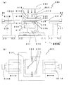
このため、従来は、例えば、ステップ露光方式で、且つ、近接露光(プロキシミティ露光)方式を採り入れた、特開平9−127702号公報に記載される、図6に示すような露光装置を用い、近接露光(プロキシミティ露光とも言う)により、相対的に原版とパターニングされる大サイズのガラス基板との位置を移動させ、原版の絵柄をずらして露光、即ちステップ露光して、パターニングを行なっていた。
尚、図6において、図6(a)は露光装置の断面図で、図6(b)は、図6(a)のB1−B2から見た上面図の概略図であり、図7は光源部の概略構成図である。 6A is a sectional view of the exposure apparatus, FIG. 6B is a schematic view of the top view as viewed from B1-B2 of FIG. 6A, and FIG. 7 is a light source. It is a schematic block diagram of a part.
図6、図7中、600は露光装置、610はステージ、611はX駆動部、612はY駆動部、613はZ駆動部、614はθ駆動部、615は基板保持部、615Aは3点アオリ調整部、615Bは基板リフトアップ部、616はマスク保持部、616Aはマスクの落下防止、620はガラス基板供給ロボット、620Aはハンド部、621はガラス基板排用ロボット、621Aはハンド部、630はガラス基板(ワーク)、640はマスク(原版)、650は光源部、650Aは光源、670はギヤップセンサー、680はスコープ、690はエッジセンサー、m1、m2、m3は反射鏡、sはシヤッター、lはフライアイレンズである。 6 and 7, 600 is an exposure apparatus, 610 is a stage, 611 is an X drive unit, 612 is a Y drive unit, 613 is a Z drive unit, 614 is a θ drive unit, 615 is a substrate holding unit, and 615A is 3 points. A tilt adjustment unit, 615B is a substrate lift-up unit, 616 is a mask holding unit, 616A is a mask drop prevention, 620 is a glass substrate supply robot, 620A is a hand unit, 621 is a glass substrate discharging robot, 621A is a hand unit, 630 Is a glass substrate (workpiece), 640 is a mask (original), 650 is a light source unit, 650A is a light source, 670 is a gap sensor, 680 is a scope, 690 is an edge sensor, m1, m2, and m3 are reflectors, s is a shutter, l is a fly-eye lens.
尚、全体を分かり易くするため、図6(a)、図6(b)においては光学系を簡略ないし省略して示している。 For easy understanding, the optical system is simplified or omitted in FIGS. 6A and 6B.
また、図6に示す露光装置は、水平方向面上において、Y方向に平行にその開口境界を設け、それぞれ、独立してX方向移動できる1対のX方向移動マスキングアパーチャ(遮光板とも言う、図9の751、752に相当)を備えたシャッターである。(図9(a)参照)
更に詳しくは、図6に示す装置は、ガラス基板630を、感光材面を上にして保持して、X、Y、Z軸方向及びθ方向に微動制御でき、且つ、少なくともX、Y方向の1方向に所定の距離だけステップ移動できるステージと、ガラス基板630上側にマスク(原版)640をマスク面を下にして保持するマスク保持部616と、マスク(原版)640の裏面かガラス基板630側へ露光光を照射するための光源部650(詳細は図6に示す)とを有し、マスク(原版)630の絵柄を等倍にて、露光する位置をずらして複数回、露光転写するための露光装置であり、ステージ610上のガラス基板630と、マスク(原版)640との位置合せを自動で行う自動アライメント機構と、原版の絵柄領域を遮蔽することにより露光領域を制御する露光領域制御機構と、該基板と原版とのギヤップを制御するギヤップ制御機構とを備えている。
The exposure apparatus shown in FIG. 6 has a pair of X-direction movement masking apertures (also referred to as light-shielding plates) that are provided with an opening boundary parallel to the Y-direction on the horizontal plane and can move independently in the X-direction. 9 corresponds to 751 and 752 in FIG. (See Fig. 9 (a))
More specifically, the apparatus shown in FIG. 6 is capable of finely controlling the glass substrate 630 in the X, Y, Z axis directions and θ directions while holding the photosensitive material surface upward, and at least in the X, Y directions. A stage that can be moved by a predetermined distance in one direction, a
そして、ガラス基板630とマスク(原版)640とを近接させ、間隔を所定のギヤップに保ちながら露光を行う近接露光にて、ガラス基板630を所定のピッチでステップ移動させ、複数の位置にてマスク(原版)640を介してガラス基板630への露光を行い、マスク原版640の絵柄をガラス基板630に転写露光するものである。
Then, the glass substrate 630 and the mask (original plate) 640 are brought close to each other, and the glass substrate 630 is stepped at a predetermined pitch in proximity exposure in which exposure is performed while maintaining a predetermined gap, and the mask is formed at a plurality of positions. (Original plate) The glass substrate 630 is exposed through the 640, and the pattern of the mask
尚、マスク(原版)640は、転写に際してのたわみが許容範囲内となるサイズである。 The mask (original plate) 640 has a size that allows the deflection during transfer to be within an allowable range.
あるいは、特開平09−141804号公報に記載されるような、マスク原版の自重によるたわみを考慮し、上記図6に示す露光装置を、マスク原版やガラス基板の面が鉛直方向に沿うように回転して配した露光装置が用いられるようになってきた。
原版マスクからガラス基板へのステップ露光方法について、ここで、1例を、図9に基づいて簡単に説明しておく。 Here, an example of the step exposure method from the original mask to the glass substrate will be briefly described with reference to FIG.
先ず、第1の位置にて、ガラス基板730とマスク740とを前述のアライメント機構とギヤップ制御機構により制御して、位置合せし、ギヤップ調整を完了した後、光源部のシヤッター(図示していない)を開放し、所定の時間だけ光源部からの光を採り入れ、マスク740の絵柄全領域(単位の絵柄領域710、8個分)を露光する第1の露光を行う。
First, at the first position, the
第1の露光によるガラス基板730での潜像は図9(b)(イ)のようになる。
The latent image on the
図9(a)(イ)のマスク740の全絵柄740Aがガラス基板側に転写される。
All the
次いで、所定のピッチだけX方向にステージ110をズラシた第2の位置にて、再度で、位置合せし、ギヤップ調整を完了した後、図9(a)(イ)に示す絵柄740Aの所定の領域のみを、マスキングアパーチャ751、752にて遮蔽した図9(a)(ロ)の状態で、所定の時間だけ光学系からの光を採り入れ、マスク740の絵柄740Aの一部領域(単位の絵柄領域710、4個分)を露光する第2の露光を行う。
Next, at the second position where the stage 110 is displaced in the X direction by a predetermined pitch, the alignment is performed again, and after completing the gap adjustment, a predetermined
第2の露光によるガラス基板730での潜像は図9(b)(ロ)のようになる。
The latent image on the
結局、第1の露光と第2の露光とによる潜像の併せて図9(b)(ハ)のようになり、目的とする図9(c)に示す絵柄740Bを得ることができる。
Eventually, the latent images of the first exposure and the second exposure are combined as shown in FIGS. 9B and 9C, and the desired
尚、710aは、単位の絵柄領域710を現像したものである。
このように、ステージをステップ移動しながら、各位置で露光を行い、合せて目的とする潜像を得る露光方式をステップ露光方式と言う。 In this way, an exposure method in which exposure is performed at each position while moving the stage stepwise to obtain a target latent image together is called a step exposure method.
表示パネルの大サイズ化が進む中、透過型の液晶表示装置においては、ますます、その画像品質の向上も求められており、局部的なムラやスジについても、その許容範囲がますます厳しく求められてきており、これに伴ない、透過型の液晶表示装置用の大サイズのカラーフィルタ基板へのフォトリソ法による、格子状のブラックマトリクスあるいは線状のブラックストライプからなる画素の境界部や、各着色層のパターニングにおいても、品質向上が求められている。 As the size of display panels is increasing, transmission-type liquid crystal display devices are increasingly required to improve their image quality, and the tolerances for local unevenness and streaks are becoming increasingly demanding. Accompanying this, by using a photolithographic method to a large-sized color filter substrate for a transmissive liquid crystal display device, the boundary between pixels formed of a grid-like black matrix or a linear black stripe, Quality improvement is also demanded in the patterning of the colored layer.
そして、最近では、局部的なムラやスジについては、画素の境界部の影響も無視できないことが分かってきた。 Recently, it has been found that the effects of pixel boundaries cannot be ignored for local unevenness and streaks.
勿論、ここでの大サイズのカラーフィルタ基板へのフォトリソ法によるパターニングの露光は、図6に示すような装置を用いステップ露光方式で、且つ、近接露光(プロキシミティ露光)方式を採り入れた露光法にて露光を行う。 Of course, the exposure of the patterning to the large color filter substrate by the photolithography method is a step exposure method using an apparatus as shown in FIG. 6 and an exposure method adopting a proximity exposure (proximity exposure) method. Exposure is performed at
尚、液晶表示装置としては、視認性が良く、カラー表示、動画表示に向いていることより、TFT(Thin Film Transistor)をアクティブ素子として各画素単位に配置し、これにより、各画素領域の液晶に独立に電圧を加え画素に明暗をつけ、画像や文字情報を表示する透過型のアクティブマトリックス方式(TFT駆動方式とも言う)とよばれる駆動方式のものが多々使用されており、通常、図4に示すような断面構造で、そのカラーフィルタ基板は、例えば、図5のような断面構造をしている。 Since the liquid crystal display device has good visibility and is suitable for color display and moving image display, a TFT (Thin Film Transistor) is arranged in each pixel unit as an active element. In many cases, a drive type called a transmission type active matrix system (also referred to as a TFT drive system) for applying an independent voltage to light and darken the pixels and displaying images and text information is used. The color filter substrate has a cross-sectional structure as shown in FIG. 5, for example.
上記のように、液晶表示装置用のカラーフィルター形成側のガラス基板側へのブラックマトリクスのフォトリソ法による形成のための露光を、図6に示すような装置を用いステップ露光方式で、且つ、近接露光(プロキシミティ露光)方式を採り入れた露光法にて露光を行う場合においても、最近では、局部的なムラやスジに影響のないものが求められている。 As described above, the exposure for forming the black matrix by the photolithographic method on the glass substrate side on the color filter forming side for the liquid crystal display device is performed by a step exposure method using an apparatus as shown in FIG. Even in the case of performing exposure using an exposure method that adopts an exposure (proximity exposure) method, recently, there is a demand for a device that does not affect local unevenness and streaks.
このようなステップ露光方式でパタンを繋いで形成された遮光パタンは、繋ぎ部に起因するムラやスジが発生する。 The light shielding pattern formed by connecting the patterns by such a step exposure method generates unevenness and streaks due to the connecting portions.
この現象は、横電界方式の液晶表示装置において特に問題となっている。 This phenomenon is particularly a problem in a horizontal electric field type liquid crystal display device.
本発明は、これに対応するもので、遮光層からなるストライプの繋ぎ部に起因する液晶表示装置での局部的なムラやスジが発生しない形態のカラーフィルタ基板を提供しようとするもので、更に具体的には、ステップ露光方式で、且つ、近接露光(プロキシミティ露光)方式を採り入れた露光法にて露光を行い、遮光層からなるストライプをフォトリソ法により形成した場合にも、露光の繋ぎ部に起因する液晶表示装置での局部的なムラやスジが発生しない形態のカラーフィルタ基板を提供しようとするものである。 The present invention, corresponding to this, is to provide a color filter substrate in a form in which local unevenness and streaks do not occur in a liquid crystal display device due to a stripe connecting portion formed of a light shielding layer. Specifically, even when a step exposure method and an exposure method adopting a proximity exposure (proximity exposure) method are used for exposure, and a stripe made of a light shielding layer is formed by a photolithographic method, the exposure joint portion The present invention is intended to provide a color filter substrate that does not cause local unevenness and streaks in a liquid crystal display device due to the above.
本発明の液晶表示装置用基板は、液晶表示装置用の基板であって、表示領域の横方向に連続した開口部と、同じく横方向に連続した遮光層からなるストライプとが、表示領域の縦方向に繰返し配列され、各遮光層からなるスライプは、所定の線幅の第1のラインと、第1のラインと同じ線幅を有し第1のラインからスライプ方向と直交する方向にずれて配置された第2のラインとが、繋ぎ部によりつながれており、且つ、前記繋ぎ部は、前記第1のラインと、前記第2のラインとが、スライプ方向と直交する方向にずれてオーバーラップしたもので、ストライプの方向と直交する方向に揃えて配されていることを特徴とするものである。 The substrate for a liquid crystal display device of the present invention is a substrate for a liquid crystal display device, wherein an opening that is continuous in the horizontal direction of the display region and a stripe that is also formed of a light shielding layer that is also continuous in the horizontal direction are vertically arranged in the display region. The stripes that are repeatedly arranged in the direction and each light-shielding layer has a first line having a predetermined line width, and the first line has the same line width as the first line, and is shifted from the first line in a direction orthogonal to the stripe direction. The arranged second line is connected by a connecting portion, and the connecting portion overlaps the first line and the second line in a direction perpendicular to the stripe direction. It is characterized by being arranged in a direction perpendicular to the direction of the stripes.
そして上記の液晶表示装置用基板であって、表示領域の縦方向に並ぶように開口部に各着色層を配し、且つ、横方向のみに遮光層からなる帯状のストライプを画素の境部に設けて、縦方向に各色の画素を配列させているカラーフィルタ形成基板であることを特徴とするものである。
また、上記のいずれかに記載の液晶表示装置用基板であって、遮光層からなるストライプのパターニングはフォトリソ法により行なわれたもので、該パターニングのための露光は、ステップ露光方式で、且つ、近接露光(プロキシミティ露光)方式を採り入れた露光法にて、ストライプの方向と直交する方向、所定幅だけ、ストライプの線方向にオーバラップさせて露光したものであることを特徴とするものである。
In the liquid crystal display substrate described above, each colored layer is arranged in the opening so as to be aligned in the vertical direction of the display area, and a strip-like stripe made of a light-shielding layer only in the horizontal direction is provided at the boundary of the pixel. And a color filter forming substrate in which pixels of each color are arranged in the vertical direction.
Further, in the liquid crystal display device substrate according to any one of the above, the patterning of the stripe formed of the light shielding layer is performed by a photolithography method, and the exposure for the patterning is a step exposure method, and The exposure method adopts a proximity exposure (proximity exposure) method, and is exposed in a direction perpendicular to the stripe direction and by a predetermined width so as to overlap in the line direction of the stripe. .
尚、ここで、表示領域の縦方向とは、表示領域の横方向に直交する方向のことである。 Here, the vertical direction of the display area is a direction orthogonal to the horizontal direction of the display area.
(作用)
本発明の液晶表示装置用基板は、このような構成にすることにより、は、ストライプの繋ぎ部に起因する液晶表示装置での局部的なムラやスジが発生しない形態のカラーフィルタ基板の提供を可能としている。
(Function)
The substrate for a liquid crystal display device of the present invention is provided with such a configuration, thereby providing a color filter substrate in a form in which local unevenness and streaks in the liquid crystal display device due to the stripe connecting portion do not occur. It is possible.
具体的には、遮光層からなるストライプのパターニングはフォトリソ法により行なわれたもので、該パターニングのための露光は、ステップ露光方式で、且つ、近接露光(プロキシミティ露光)方式を採り入れた露光法にて、ストライプの方向と直交する方向、所定幅だけ、ストライプの線方向にオーバラップさせて露光したものである場合に、露光のつなぎ部に起因する液晶表示装置での局部的なムラやスジが発生しない液晶表示装置用のカラーフィルタ基板の提供を可能としている。 Specifically, the patterning of the stripe made of the light shielding layer is performed by a photolithography method, and the exposure for the patterning is an exposure method adopting a step exposure method and a proximity exposure (proximity exposure) method. In this case, when the exposure is performed in the direction orthogonal to the stripe direction and overlapped in the line direction of the stripe by a predetermined width, local unevenness and streaks in the liquid crystal display device due to the connection portion of the exposure are obtained. It is possible to provide a color filter substrate for a liquid crystal display device in which no occurrence occurs.
本発明は、上記のように、遮光層からなるストライプの繋ぎ部に起因する液晶表示装置での局部的なムラやスジが発生しない形態のカラーフィルタ基板の提供を可能とした。 As described above, the present invention makes it possible to provide a color filter substrate in a form in which local unevenness and streaks are not generated in the liquid crystal display device due to the stripe connecting portion formed of the light shielding layer.
更に具体的には、ステップ露光方式で、且つ、近接露光(プロキシミティ露光)方式を採り入れた露光法にて露光を行い、遮光層からなるストライプをフォトリソ法により形成した場合にも、露光の繋ぎ部に起因する液晶表示装置での局部的なムラやスジが発生しない形態のカラーフィルタ基板の提供を可能とした。 More specifically, exposure is performed even when exposure is performed by a step exposure method and an exposure method adopting a proximity exposure (proximity exposure) method, and a stripe made of a light shielding layer is formed by a photolithography method. It is possible to provide a color filter substrate in a form in which local unevenness and streaks are not generated in the liquid crystal display device due to the portion.
特に、遮光層からなるストライプと、隣合うストライプ間に1ヶ所以上の屈曲部を有する着色層と、この着色層上に柱状スペーサを有する構成は、遮光パタンの繋ぎ部に起因するムラやスジが発生せず、視野角依存性が少なく、さらにギャップムラが発生しない横電界方式の液晶表示装置に好適なカラーフィルタ基板の提供を可能とした。 In particular, the configuration including a stripe made of a light shielding layer, a colored layer having one or more bent portions between adjacent stripes, and a columnar spacer on the colored layer has unevenness and streaks due to the joint portion of the light shielding pattern. It is possible to provide a color filter substrate suitable for a horizontal electric field type liquid crystal display device that does not occur, has little viewing angle dependency, and does not generate gap unevenness.
本発明の実施の形態例を図に基づいて説明する。 Embodiments of the present invention will be described with reference to the drawings.
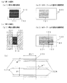
図1(a)は本発明の液晶表示装置用基板の概略全体図で、図1(b)は画素部の一部(繋ぎ部のない領域)を示した図で、図1(c)はストライプの繋ぎ部における状態を示した図で、図2は本発明の液晶表示装置用基板のストライプのパターニング方法の実施の形態の1例を説明するための図で、図2(a1)は第1の露光における原版の露光領域を示し、図2(a2)は第1の露光による潜像形成状態を示し、図2(b1)は第2の露光における原版の露光領域領域を示し、図2(b2)は第2の露光による潜像形成状態を示し、図2(c)は図2(b2)の第1の露光と第2の露光の境界部を含む領域A1の一部拡大図であり、図3は第1の比較例のストライプのパターニングにおける露光状態(潜像状態)を示した図である。 図1、図2、図3において、10は液晶表示装置用基板(カラーフィルタ基板)、11は基板、15は表示領域(画素領域とも言う)、20はストライプ、25は繋ぎ部、30は画素、31はR着色画素部、32はG着色画素部、33はB着色画素部、40は着色層、41はR着色層、42はG着色層、43はB着色層、110は原版、111はパターン部、112は遮光部、120は(カラーフィルタ基板用の)基板、121は第1の露光による潜像、121Aは(第1の露光による)ストライプパターン潜像、122は第2の露光による潜像、122Aは(第2の露光による)ストライプパターン潜像、125は(第の露光領域と第2の露光領域との)境界部、131、132はマスキングアパーチャ、221は(第1の露光による)ストライプパターン潜像、222は(第2の露光による)ストライプパターン潜像、α1、α2はパターンずれである。 FIG. 1A is a schematic overall view of a substrate for a liquid crystal display device of the present invention, FIG. 1B is a view showing a part of a pixel portion (region without a connecting portion), and FIG. FIG. 2 is a diagram illustrating a state at a stripe connecting portion. FIG. 2 is a diagram for explaining an example of an embodiment of a method for patterning a stripe of a substrate for a liquid crystal display device according to the present invention. FIG. 2 shows the exposure area of the original in the first exposure, FIG. 2A2 shows the latent image formation state by the first exposure, FIG. 2B1 shows the exposure area of the original in the second exposure, and FIG. (B2) shows a latent image formation state by the second exposure, and FIG. 2 (c) is a partially enlarged view of the area A1 including the boundary between the first exposure and the second exposure in FIG. 2 (b2). FIG. 3 is a view showing an exposure state (latent image state) in the patterning of the stripe of the first comparative example. 1, 2, and 3, 10 is a substrate for a liquid crystal display device (color filter substrate), 11 is a substrate, 15 is a display region (also referred to as a pixel region), 20 is a stripe, 25 is a connecting portion, and 30 is a pixel. , 31 is an R colored pixel portion, 32 is a G colored pixel portion, 33 is a B colored pixel portion, 40 is a colored layer, 41 is an R colored layer, 42 is a G colored layer, 43 is a B colored layer, 110 is an original plate, 111 Is a pattern portion, 112 is a light shielding portion, 120 is a substrate (for a color filter substrate), 121 is a latent image by a first exposure, 121A is a stripe pattern latent image (by a first exposure), and 122 is a second exposure. , 122A is a stripe pattern latent image (by the second exposure), 125 is a boundary portion (between the first exposure region and the second exposure region), 131 and 132 are masking apertures, and 221 is (the first exposure region) By exposure) Ripe pattern latent image, 222 (the second exposure) stripe pattern latent image, [alpha] 1, [alpha] 2 is a pattern shift.
本発明の液晶表示装置用基板の実施の形態の1例を図1に基づいて説明する。 An example of an embodiment of a substrate for a liquid crystal display device of the present invention will be described with reference to FIG.
本例の液晶表示装置用基板10は、透過型の液晶表示装置用のカラーフィルタ基板で、表示領域15の縦方向(図1(a)の表示領域短辺方向)にR着色層41、G着色層42、B着色層43をそれぞれ帯状に配し、且つ、それら着色層に直交する横方向のみに遮光層からなる帯状のストライプ20を画素30の境部に設けて、図1(b)に示すように、前記縦方向に長い形状の画素を配列させているもので、ストライプ20の方向と直交する縦方向に揃えて、各ストライプ20は、所定幅Lで、その線方向にオーバラップする繋ぎ部25(図1(c)に示す)を、設けているものである。
The substrate 10 for the liquid crystal display device of this example is a color filter substrate for a transmissive liquid crystal display device, and has an R colored
本例の液晶表示装置用基板10は、遮光層からなるストライプ20のパターニングはフォトリソ法により行なわれたもので、そのパターニングのための露光は、ステップ露光方式で、且つ、近接露光(プロキシミティ露光)方式を採り入れた露光法にて、ストライプの方向と直交する方向、所定幅だけ、ストライプ20の線方向にオーバラップさせて露光したものである。
In the liquid crystal display substrate 10 of this example, the patterning of the
このような露光方法にて、オーバーラップして露光され、パターニングされたもので、繋ぎ部においては、露光ずれが発生し、現像処理あるいは現像処理とエッチング処理を経て、図1(c)に示すように、所定幅Lの部分だけ他の箇所よりも、ストライプが太くなる。 In such an exposure method, they are exposed and patterned in an overlapping manner, and an exposure shift occurs in the joint portion, and after development processing or development processing and etching processing, it is shown in FIG. In this way, the stripe is thicker than the other portions only by the portion of the predetermined width L.
尚、基板としては、通常、ガラス基板が用いられるが、透過率、熱膨張率等の特性や処理性や耐性が良いものであればこれに限定はされない。 A glass substrate is usually used as the substrate, but is not limited to this as long as it has good properties such as transmittance and thermal expansion, processability, and resistance.
遮光層からなるストライプ20としては、通常、クロムや酸化クロム、窒化クロム、酸化窒化クロムやこれらを積層した金属層をフォトリソ法にて、パターンニングし、更にエッチングして形成、あるいは、黒色感光材を塗布しこれをフォトリソ法にてパターン形成する。
The
R着色層41、G着色層42、B着色層43は、染色形成、顔料分散感光材を製版形成、印刷形成、電着形成等により形成され、特に限定はされない。
The R colored
本例の液晶表示装置用基板10は、横電界方式の液晶表示装置用カラーフィルタ基板として好適に用いられる。 The substrate 10 for a liquid crystal display device of this example is preferably used as a color filter substrate for a liquid crystal display device of a horizontal electric field type.
横電界方式の液晶表示装置用カラーフィルタ基板においては、遮光層からなるストライプの材料としては、黒色顔料として酸化チタンを含むネガ型感光性樹脂が、繋ぎ部のパタンのずれが目立ちにくいため好ましい。 In a color filter substrate for a horizontal electric field type liquid crystal display device, a negative photosensitive resin containing titanium oxide as a black pigment is preferable as a stripe material made of a light-shielding layer because the shift of the pattern of the joint portion is not noticeable.
この方式の場合、遮光層からなる隣合うストライプ間に1ヶ所以上の屈曲部を有する着色層は、アクティブ素子側基板の電極の屈曲角度とほぼ同一の角度が好ましい。 In the case of this method, the colored layer having one or more bent portions between adjacent stripes made of the light shielding layer preferably has an angle substantially the same as the bent angle of the electrode of the active element side substrate.
また、柱状スペーサは、開口部上にあってもよいが、遮光層からなるストライプ上に形成するのが好ましい。 The columnar spacer may be on the opening, but is preferably formed on a stripe made of a light shielding layer.
また着色層上に平坦化保護層を設け、その上に柱状スペーサを形成することが、さらに好ましい。 It is further preferable to provide a planarization protective layer on the colored layer and form a columnar spacer thereon.
尚、柱状スペーサは、液晶を封止する際の、および封止以降のギャップを制御するためのものである。 The columnar spacer is for controlling a gap when sealing the liquid crystal and after sealing.
縦方向に同一色の着色層を配列する方法としては、3色すべて帯状、3色すべて独立したパタン、以上いずれの配列をとることもできる。 As a method of arranging colored layers of the same color in the vertical direction, all three colors can be strip-like, all three colors can be independent patterns, and any of the above arrangements can be used.
本例の液晶表示装置用基板10のストライプのパターニングにおける露光方法を図2に基づいて説明する。 An exposure method in the patterning of the stripe of the substrate 10 for the liquid crystal display device of this example will be described with reference to FIG.
フォトリソ法により、ストライプ形成のためのパターンニングを行うもので、露光方法は、ステップ露光方式で、且つ、近接露光(プロキシミティ露光)方式を採り入れた露光法にて、図6に示す露光装置を用いて行うものである。 The patterning for forming stripes is performed by photolithography, and the exposure method is a step exposure method and an exposure method adopting a proximity exposure (proximity exposure) method. Is what you do.
そして、基板120に形成する所望のパターン領域よりも小さい、パターン領域111を有する原版110を用いて、基板120に所望のパターンを形成するもので、先ず原版のパターン領域全体を露光する第1の露光を行い、次いで、図6に示すステージ610を移動し、且つ、原版110を第1の露光の位置と同じ位置に固定したまま、その露光範囲をマスキングアパーチャ131、132により制限して、一部露光領域をオーバーラップさせて、所定の露光領域に第2の露光を行うものである。
Then, a desired pattern is formed on the substrate 120 using the original 110 having the
この際、繋ぎ部となる領域をオーバーラップさせる露光は、ストライプの線方向を、所定幅OL1だけオーバーラップさせるもので、図2(b2)に示すA1部は図2(c)のようになる。 In this case, the exposure for overlapping the region to be the connecting portion is to overlap the stripe line direction by a predetermined width OL1, and the A1 portion shown in FIG. 2 (b2) is as shown in FIG. 2 (c). .
この場合、ストライプパターン潜像121Aとストライプパターン潜像122Aとのずれ量がα1とすると、現像処理あるいは現像処理とエッチング処理を経てストライプを形成した場合、このオーバーラップ領域における透過光の減少率は、ストライプパターンの線幅、ピッチを、それぞれW1、P1とすれば、α1/(P1ーW1)となる。 In this case, assuming that the shift amount between the stripe pattern latent image 121A and the stripe pattern latent image 122A is α1, when the stripe is formed through the development process or the development process and the etching process, the reduction rate of the transmitted light in this overlap region is If the line width and pitch of the stripe pattern are W1 and P1, respectively, α1 / (P1−W1).
一方、第1の比較例として、透過型の液晶表示装置用のカラーフィルタ基板で、表示領域15の縦方向(図1(a)の表示領域15短方向)にR着色層41、G着色層42、B着色層43をそれぞれ帯状に配し、且つ、それら着色層に沿う方向直のみ、画素の境界に、遮光層からなる帯状のストライプを設けたものも挙げられる。
On the other hand, as a first comparative example, a color filter substrate for a transmissive liquid crystal display device, an R colored
この場合も、図1に示す実施例と同じように、パターニングが行なわれるとし、ストライプパターンの線方向に直交する方向に所定幅OL2だけオーバーラップさせる露光を行うと、潜像の重なりは図3に示すようになり、第1の露光によるストライプパターン潜像221と第2の露光によるストライプパターン潜像222とのずれ量がα2とすると、現像処理あるいは現像処理とエッチング処理を経てストライプを形成した場合、このオーバーラップ領域における透過光の減少率は、ストライプパターンの線幅、ピッチをW2、P2とすれば、α2/(P2ーW2)となる。 Also in this case, as in the embodiment shown in FIG. 1, it is assumed that patterning is performed. When exposure is performed so as to overlap by a predetermined width OL2 in the direction orthogonal to the line direction of the stripe pattern, the overlapping of the latent images is as shown in FIG. As shown in FIG. 2, when the amount of deviation between the stripe pattern latent image 221 by the first exposure and the stripe pattern latent image 222 by the second exposure is α2, stripes are formed through development processing or development processing and etching processing. In this case, the reduction rate of the transmitted light in the overlap region is α2 / (P2−W2) if the line width and pitch of the stripe pattern are W2 and P2.
ここで、W1=W2、P1=P2、α1=α2とすれば、透過率の減少の面では、本例と図3に示す潜像を得る比較例の露光方法とは差はないが、潜像が形成された後、現像処理、あるいは現像処理とエッチング処理を更に行い、パターン形成されたストライプ形成基板や、更に着色層を形成されたカラーフィルタ基板について、ライトテーブルを用いて透過光にて視覚検査を行なって場合、ムラ、スジは、本例のカラーフィルタ基板の方が、第1の比較例のものに比べ格段に良好である。 Here, if W1 = W2, P1 = P2, and α1 = α2, there is no difference between the exposure method of this example and the comparative example for obtaining the latent image shown in FIG. After the image is formed, the development process, or the development process and the etching process are further performed, and the patterned stripe-formed substrate and the color filter substrate on which the colored layer is further formed are transmitted using a light table. When visual inspection is performed, unevenness and streaks are much better in the color filter substrate of this example than in the first comparative example.
視覚検査は、ストライプの方向は液晶表示装置の上下方向で、画素の長手方向方向を人が見る上下方向として検査を行うもので、人の視覚の特性からこのような結果が得られると思われる。 In the visual inspection, the stripe direction is the vertical direction of the liquid crystal display device, and the longitudinal direction of the pixel is the vertical direction to be seen by a person, and such a result seems to be obtained from human visual characteristics. .
カラーフィルタ基板の画素の境界形態の別の例としては、透過型の液晶表示装置用のカラーフィルタ基板の、各着色層の境界に位置する格子状に遮光層からなるブラックマトリクスを備えたものが第2の比較例として挙げられる。 As another example of the pixel boundary shape of the color filter substrate, a color filter substrate for a transmissive liquid crystal display device having a black matrix composed of a light shielding layer in a lattice shape located at the boundary of each colored layer. As a second comparative example.
これは、実施の形態例のストライプと第1の比較例のストライプとを合せ設け、画素の境界部に格子状にした形態のものである。 This is a configuration in which the stripes of the embodiment and the stripes of the first comparative example are provided together and are formed in a lattice pattern at the boundary of the pixels.
第2の比較例についても、先に述べたライトテーブルを用いた視覚検査方法で、第1の比較例の場合と同様、実施の形態例のものに比べ、ムラ、スジの面で劣るという結果が得られた。 As for the second comparative example, the visual inspection method using the light table described above is inferior in terms of unevenness and streaks as compared with the first embodiment, as in the case of the first comparative example. was gotten.
尚、原版マスクとしては、所定のサイズの乾板やクロム等の遮光膜、感光剤をこの順に配設したガラス基板基板等に、データを用いて露光を行う露光装置にて露光描画し、現像され、ないし、現像、エッチングされ、パターニングされたものもの(オリジナルとも言う)、あるいは、該オリジナルから別の乾板やクロム等の遮光膜、感光剤をこの順に配設したガラス基板基板に密着露光により転写する工程を1回以上用いて、パターニング形成されたものもの(コピーとも言う)を用いる。
In addition, as an original mask, exposure drawing is carried out by an exposure apparatus that performs exposure using data on a dry plate of a predetermined size, a light shielding film such as chromium, a glass substrate substrate in which a photosensitizer is arranged in this order, and developed. Developed, etched and patterned (also referred to as the original), or transferred from the original to a glass substrate substrate in which another dry plate, a light shielding film such as chromium, and a photosensitizer are arranged in this order by contact exposure A patterning process (also called a copy) is used at least once.
10 液晶表示装置用基板(カラーフィルタ基板)
11 基板
15 表示領域(画素領域とも言う)
20 ストライプ
25 繋ぎ部
30 画素
31 R着色画素部
32 G着色画素部
33 B着色画素部
40 着色層
41 R着色層
42 G着色層
43 B着色層
110 原版
111 パターン部
112 遮光部
120 (カラーフィルタ基板用の)基板
121 第1の露光により潜像
121A (第1の露光による)ストライプパターン潜像
122 第2の露光による潜像
122A (第2の露光による)ストライプパターン潜像
125 (第の露光領域と第2の露光領域との)境界部
131、132 マスキングアパーチャ
221 (第1の露光による)ストライプパターン潜像
222 (第2の露光による)ストライプパターン潜像
α1、α2 パターンずれ
10 Liquid crystal display substrate (color filter substrate)
11 Substrate 15 Display area (also referred to as pixel area)
20
Claims (3)
Priority Applications (1)
| Application Number | Priority Date | Filing Date | Title |
|---|---|---|---|
| JP2003331068A JP4306385B2 (en) | 2003-09-24 | 2003-09-24 | Substrate for liquid crystal display |
Applications Claiming Priority (1)
| Application Number | Priority Date | Filing Date | Title |
|---|---|---|---|
| JP2003331068A JP4306385B2 (en) | 2003-09-24 | 2003-09-24 | Substrate for liquid crystal display |
Publications (2)
| Publication Number | Publication Date |
|---|---|
| JP2005099232A JP2005099232A (en) | 2005-04-14 |
| JP4306385B2 true JP4306385B2 (en) | 2009-07-29 |
Family
ID=34459827
Family Applications (1)
| Application Number | Title | Priority Date | Filing Date |
|---|---|---|---|
| JP2003331068A Expired - Fee Related JP4306385B2 (en) | 2003-09-24 | 2003-09-24 | Substrate for liquid crystal display |
Country Status (1)
| Country | Link |
|---|---|
| JP (1) | JP4306385B2 (en) |
Families Citing this family (2)
| Publication number | Priority date | Publication date | Assignee | Title |
|---|---|---|---|---|
| JP5471222B2 (en) * | 2009-09-15 | 2014-04-16 | 株式会社ニコン | Optical element manufacturing method |
| KR102100261B1 (en) * | 2013-11-13 | 2020-04-13 | 엘지디스플레이 주식회사 | Organic light emitting diode display device and repairing method thereof |
-
2003
- 2003-09-24 JP JP2003331068A patent/JP4306385B2/en not_active Expired - Fee Related
Also Published As
| Publication number | Publication date |
|---|---|
| JP2005099232A (en) | 2005-04-14 |
Similar Documents
| Publication | Publication Date | Title |
|---|---|---|
| JP3207136B2 (en) | Liquid crystal display | |
| KR101984898B1 (en) | Method of fabricating display device using maskless exposure apparatus and display device | |
| JP4697960B2 (en) | Patterning method and original mask for proximity exposure used therefor | |
| US20170315451A1 (en) | Divisional exopsure apparatus and method of manufacturing liquid crystal display using the same | |
| JP2008281919A (en) | Method of forming color filter forming substrate and color filter forming substrate | |
| TWI470379B (en) | Exposure method, method for manufacturing color filter, and exposure device | |
| US20120026435A1 (en) | Color filter and color filter manufacturing method | |
| JP4957020B2 (en) | Manufacturing method of color filter for liquid crystal display device and color filter for liquid crystal display device | |
| JP4736277B2 (en) | Method for forming colored pixels of color filter and method for forming black matrix of color filter | |
| JP4306385B2 (en) | Substrate for liquid crystal display | |
| JP4593214B2 (en) | Method for patterning substrate for liquid crystal display device, substrate for liquid crystal display device, and liquid crystal display device | |
| TWI398737B (en) | Method of mask alignment and exposing and mask assembly | |
| US20170329177A1 (en) | Liquid Crystal Display Panel, Liquid Crystal Display Apparatus, and Method of Manufacturing Liquid Crystal Display Panel | |
| KR101343292B1 (en) | Substrate for photomask, photomask and pattern transfer method | |
| JP4816885B2 (en) | Manufacturing method of color filter for liquid crystal display device | |
| JP2005084492A (en) | Photomask for color filter and method for manufacturing color filter using the same | |
| JP2020021017A (en) | Color filter and manufacturing method thereof | |
| JP2005091790A (en) | Exposing method for columnar spacer formation, color filter formation substrate for liquid crystal display device, and liquid crystal display device | |
| JP2001159755A (en) | Liquid crystal display device and method of producing the same | |
| JP5217648B2 (en) | Photomask and color filter substrate manufactured using the same | |
| JP5217154B2 (en) | Color filter manufacturing method and color filter | |
| JP2010008532A (en) | Half tone photomask and color filter substrate produced by using it | |
| JP5581017B2 (en) | Exposure method and exposure apparatus | |
| WO2014132819A1 (en) | Method for manufacturing color filter, and liquid crystal display device | |
| JP5163153B2 (en) | Photomask for color filter and method for producing color filter |
Legal Events
| Date | Code | Title | Description |
|---|---|---|---|
| A621 | Written request for application examination |
Free format text: JAPANESE INTERMEDIATE CODE: A621 Effective date: 20060925 |
|
| A977 | Report on retrieval |
Free format text: JAPANESE INTERMEDIATE CODE: A971007 Effective date: 20081208 |
|
| A131 | Notification of reasons for refusal |
Free format text: JAPANESE INTERMEDIATE CODE: A131 Effective date: 20081216 |
|
| A521 | Written amendment |
Free format text: JAPANESE INTERMEDIATE CODE: A523 Effective date: 20090127 |
|
| TRDD | Decision of grant or rejection written | ||
| A01 | Written decision to grant a patent or to grant a registration (utility model) |
Free format text: JAPANESE INTERMEDIATE CODE: A01 Effective date: 20090422 |
|
| A01 | Written decision to grant a patent or to grant a registration (utility model) |
Free format text: JAPANESE INTERMEDIATE CODE: A01 |
|
| A61 | First payment of annual fees (during grant procedure) |
Free format text: JAPANESE INTERMEDIATE CODE: A61 Effective date: 20090427 |
|
| R150 | Certificate of patent or registration of utility model |
Free format text: JAPANESE INTERMEDIATE CODE: R150 Ref document number: 4306385 Country of ref document: JP Free format text: JAPANESE INTERMEDIATE CODE: R150 |
|
| FPAY | Renewal fee payment (event date is renewal date of database) |
Free format text: PAYMENT UNTIL: 20120515 Year of fee payment: 3 |
|
| FPAY | Renewal fee payment (event date is renewal date of database) |
Free format text: PAYMENT UNTIL: 20120515 Year of fee payment: 3 |
|
| FPAY | Renewal fee payment (event date is renewal date of database) |
Free format text: PAYMENT UNTIL: 20130515 Year of fee payment: 4 |
|
| FPAY | Renewal fee payment (event date is renewal date of database) |
Free format text: PAYMENT UNTIL: 20140515 Year of fee payment: 5 |
|
| LAPS | Cancellation because of no payment of annual fees |