JP4292898B2 - Communication device - Google Patents
Communication device Download PDFInfo
- Publication number
- JP4292898B2 JP4292898B2 JP2003193432A JP2003193432A JP4292898B2 JP 4292898 B2 JP4292898 B2 JP 4292898B2 JP 2003193432 A JP2003193432 A JP 2003193432A JP 2003193432 A JP2003193432 A JP 2003193432A JP 4292898 B2 JP4292898 B2 JP 4292898B2
- Authority
- JP
- Japan
- Prior art keywords
- data
- wavelet
- complex
- transmission
- transformer
- Prior art date
- Legal status (The legal status is an assumption and is not a legal conclusion. Google has not performed a legal analysis and makes no representation as to the accuracy of the status listed.)
- Expired - Fee Related
Links
Images


Description
【0001】
【発明の属する技術分野】
本発明は、実係数ウェーブレットフィルタバンクを用いたディジタル変復調処理によりデータ伝送を行うマルチキャリア伝送方法(Digital Wavelet Multi Carrier伝送方法、以下、「DWMC伝送方法」と記載する)を用いる通信装置に関する。
【0002】
【従来の技術】
実係数ウェーブレットフィルタバンクを用いたディジタル変復調処理による伝送方法は、マルチキャリア変調方法の一種であり、実係数フィルタバンクにより複数のディジタル変調波を合成して送信信号を生成するものである。各キャリアの変調方式としては、PAM(Pulse Amplitude Modulation)が用いられる。
【0003】
DWMC伝送方法によるデータ伝送について、図15〜図18を用いて説明する。図15はウェーブレット波形の例を示す波形図であり、図16はDWMC伝送方法における送信波形の例を示す波形図、図17はDWMC伝送方法における送信スペクトルの例を示すスペクトル図、図18はDWMC伝送方法における送信フレームの構成例を示すフレーム図である。
【0004】
DWMC伝送方法によるデータ伝送は、図15に示すように、各サブキャリアのインパルス応答が各サブキャリア内で重なり合いながら伝送される。各伝送シンボルは、図16に示すように、各サブキャリアのインパルス応答が合成された時間波形となる。図17に振幅スペクトルの例を示す。DWMC伝送方法では、図16の伝送シンボルを数十個〜数百個程度集めて1つの伝送フレームを構成する。DWMC伝送フレームの構成例を図18に示す。このDWMC伝送フレームには、情報データ伝送用シンボルの他にフレーム同期用シンボルや等化用シンボルなどが含まれる。
【0005】
図14は、DWMC伝送方法を採用した場合の送信装置299および受信装置199から成る従来の通信装置を示すブロック図である。
【0006】
図14において、110はA/D変換器、120はウェーブレット変換器、130はパラレルデータをシリアルデータに変換するP/S変換器、140は受信信号の判定を行う判定器、210はビットデータをシンボルデータに変換しシンボルマッピングを行うシンボルマッパ、220はシリアルデータをパラレルデータに変換するS/P変換器、230は逆ウェーブレット変換器、240はD/A変換器である。
【0007】
このように構成された通信装置について、その動作を説明する。
【0008】
まず、送信装置299においては、シンボルマッパ210によってビットデータをシンボルデータに変換し、各シンボルデータに従ってシンボルマッピング(PAM変調)を行う。そして、直列並列変換器(S/P変換器)220でサブキャリアごとに実数値di(i=1〜M、Mは複数)を与え、逆ウェーブレット変換器230で時間軸上へ逆離散ウェーブレット変換する。これにより、時間軸波形のサンプル値を発生させ、伝送シンボルを表すサンプル値系列を生成する。D/A変換器240で、このサンプル値系列から時間的に連続するベースバンド・アナログ信号波形に変換して送信する。ここで、逆離散ウェーブレット変換により発生される時間軸上のサンプル値の個数は、通常2のn乗(nは正の整数)個である。
【0009】
受信装置199においては、受信信号をA/D変換器110でディジタルベースバンド信号波形を得た後、送信側と同じサンプルレートでサンプルする。そして、このサンプル値系列をウェーブレット変換器120により周波数軸上へ離散ウェーブレット変換し、その後並直列変換器(P/S変換器)130により直列に変換する。最後に判定器140にて各サブキャリアの振幅値を計算し、受信信号の判定を行って受信データを得る。
【0010】
ところで、通信においては、伝送路のインピーダンス変動やマルチパスなどの影響により振幅歪みや位相歪みが生じるため、振幅、位相の両パラメータ、すなわち複素情報を扱えた方が都合がよい。これに対して、従来のDWMC伝送方法では、振幅情報しか扱えないため、伝送路の状態によっては歪みを補正することができず、伝送効率が大幅に抑制されてしまうといった問題がある(例えば、非特許文献1参照。)。
【0011】
【非特許文献1】
貴家仁志著「ディジタル信号処理シリーズ14 マルチレート信号処理」昭晃堂発行,1995年10月6日,P186−190
【0012】
【発明が解決しようとする課題】
このように、従来の実係数フィルタバンクによる伝送方法を用いる通信装置では、伝送用データとして振幅情報のみしか扱えず、受信装置で複素情報を扱った処理を行うことができないという問題点を有していた。
【0013】
この通信装置では、複素情報を扱えるDWMC伝送方法を用いることが要求されている。
【0014】
本発明は、この要求を満たすため、複素情報を扱えるDWMC伝送方法を用いる通信装置を提供することにある。
【0015】
【課題を解決するための手段】
この課題を解決するために本発明の通信装置は、ディジタルマルチキャリア復調処理を行う受信装置を有し、実係数ウェーブレットフィルタバンクを用いたディジタルマルチキャリア変復調処理によりデータ伝送を行うマルチキャリア伝送方法を用いた通信装置であって、前記受信装置は検波部を有し、前記検波部は、受信波形データをウェーブレット変換する互いに直交する複数M個の実係数ウェーブレットフィルタで構成される第1のウェーブレット変換器と、前記受信波形データをヒルベルト変換するヒルベルト変換器と、前記ヒルベルト変換器からの出力をウェーブレット変換する第2のウェーブレット変換器と、前記第1のウェーブレット変換器からの出力を複素情報の同相成分とし、前記第2のウェーブレット変換器からの出力を直交成分として複素データを生成する複素データ生成器とを有する構成を備えている。
【0016】
これにより、複素情報を扱えるDWMC伝送方法を用いる通信装置が得られる。
【0017】
【発明の実施の形態】
本発明の請求項1に記載の通信装置は、ディジタルマルチキャリア復調処理を行う受信装置を有し、実係数ウェーブレットフィルタバンクを用いたディジタルマルチキャリア変復調処理によりデータ伝送を行うマルチキャリア伝送方法を用いた通信装置であって、受信装置は検波部を有し、検波部は、受信波形データをウェーブレット変換する互いに直交する複数M個の実係数ウェーブレットフィルタで構成される第1のウェーブレット変換器と、受信波形データをヒルベルト変換するヒルベルト変換器と、ヒルベルト変換器からの出力をウェーブレット変換する第2のウェーブレット変換器と、第1のウェーブレット変換器からの出力を複素情報の同相成分とし、第2のウェーブレット変換器からの出力を直交成分として複素データを生成する複素データ生成器と、第2のウェーブレット変換器からのM個の出力の奇数番目の出力を符号反転する符号変換器とを有することとしたものである。
【0018】
この構成により、受信装置に到来する実信号のみの時間信号からサブキャリア毎の複素情報を得ることができるので、高精度な復調を行うことができ、また、振幅値のみでなく位相情報も処理の対象とすることができるようになるため、群遅延などによって生じる劣悪な伝送路によって各サブキャリアの同期タイミングずれが生じた場合でもサブキャリア毎に位相回転分を補正して受信性能を向上させることができるという作用を有する。
【0021】
請求項2に記載の通信装置は、符号変換器からの出力についてヒルベルト変換器のリプルによる振幅変動を補正するレベル変換器を更に有することを特徴とする請求項1に記載の通信装置である。
【0022】
この構成により、受信装置に到来する実信号のみの時間信号からサブキャリア毎の複素情報を得ることができるので、高精度な復調を行うことができ、また、振幅値のみでなく位相情報も処理の対象とすることができるようになるため、群遅延などによって生じる劣悪な伝送路によって各サブキャリアの同期タイミングずれが生じた場合でもサブキャリア毎に位相回転分を補正して受信性能を向上させることができるという作用を有する。
【0023】
請求項3に記載の通信装置は、ディジタルマルチキャリア復調処理を行う受信装置を有する実係数ウェーブレットフィルタバンクを用いたディジタルマルチキャリア変復調処理によりデータ伝送を行うマルチキャリア伝送方法を用いた通信装置であって、受信装置は検波部を有し、検波部は、受信波形データをウェーブレット変換する互いに直交する複数M個の実係数ウェーブレットフィルタで構成される第1のウェーブレット変換器と、受信波形データに対してヒルベルト変換、ウェーブレット変換、奇数番目の符号の反転を行うウェーブレットフィルタで構成される第2のウェーブレット変換器と、第1のウェーブレット変換器からの出力を複素情報の同相成分とし、第2のウェーブレット変換器からの出力を直交成分として複素データを生成する複素データ生成器とを有することとしたものである。
【0024】
この構成により、受信装置に到来する実信号のみの時間信号からサブキャリア毎の複素情報を得ることができるので、高精度な復調を行うことができ、また、請求項1に記載の通信装置におけるよりも高速な処理を行うことができ、回路構成を簡素化することができるという作用を有する。
【0027】
請求項4に記載の通信装置は、請求項1に記載の通信装置において、第2のウェーブレット変換器は、実係数を有するポリフェーズフィルタで構成されたプロトタイプフィルタと、複数M個のダウンサンプラと、M−1個の1サンプル遅延素子と、入力系列の順番をM個単位で反転させる時系列反転器と、高速M点の離散コサイン変換器とを有することとしたものである。
【0028】
この構成により、第1のウェーブレット変換器の高速M点離散コサイン変換器を共用することができるという作用を有する。
【0029】
請求項5に記載の通信装置は、ディジタルマルチキャリア復調処理を行う受信装置を有し、実係数ウェーブレットフィルタバンクを用いたディジタルマルチキャリア変復調処理によりデータ伝送を行うマルチキャリア伝送方法を用いた通信装置であって、受信装置は、請求項1乃至3のいずれか1に記載の検波部と、検波部から得られる複素情報と等化処理用にあらかじめ割り当てられた等化用既知信号とを用いて等化を行う等化器と、等化器から得られる信号を用いて判定を行う判定器とを有することしたものである。
【0030】
この構成により、複素情報と等化用既知信号とを用いて等化を行うことができるので、劣悪な伝送路においても高精度な復調を行うことができるという作用を有する。
【0031】
請求項6に記載の通信装置は、ディジタルマルチキャリア変調処理を行う送信装置とディジタルマルチキャリア復調処理を行う受信装置とを有し、実係数ウェーブレットフィルタバンクを用いたディジタルマルチキャリア変復調処理によりデータ伝送を行うマルチキャリア伝送方法を用いた通信装置であって、送信装置は、連続する数シンボルの間に渡って同一で且つ受信装置で既知の同期用データを発生する同期用データ発生器と、同期用データを逆ウェーブレット変換する逆ウェーブレット変換器とを有し、受信装置は、請求項1乃至5のいずれか1に記載の検波部と、検波部から得られる複素情報と等化処理用にあらかじめ割り当てられた等化用既知信号とを用いて等化を行う等化器と、等化器から得られる信号を用いて判定を行う判定器と、検波部より出力される隣接する複素サブキャリア間の位相差からシンボル同期タイミングを推定する同期推定回路とを有することとしたものである。
【0032】
この構成により、同じキャリア番号がついた第1のウェーブレットフィルタバンクより得られるサブキャリアと第2のウェーブレットフィルタバンクより得られるサブキャリアとで構成される複素サブキャリアにおいて、複素サブキャリア間の位相差からシンボル同期タイミングを推定することができるので、正確かつ高精度の復調を行うことができるという作用を有する。
【0033】
請求項7に記載の通信装置は、ディジタルマルチキャリア変調処理を行う送信装置とディジタルマルチキャリア復調処理を行う受信装置とを有し、実係数ウェーブレットフィルタバンクを用いたディジタルマルチキャリア変復調処理によりデータ伝送を行うマルチキャリア伝送方法を用いた通信装置であって、送信装置は、連続する数シンボルの間に渡って同一で且つ受信装置で既知の同期用データを発生する同期用データ発生器と、同期用データを逆ウェーブレット変換する逆ウェーブレット変換器とを有し、受信装置の検波部は、受信波形データをウェーブレット変換する互いに直交する複数M個の実係数ウェーブレットフィルタで構成されるウェーブレット変換器と、ウェーブレット変換器からの2n−1番目(nは正の整数)の出力を複素情報の同相成分とし、2n番目の出力を直交成分として(但し、1≦n≦(M/2−1)、サブキャリア番号を0〜M−1とする)複素データを生成する複素データ生成器とを有することとしたものである。
【0034】
この構成により、受信装置に到来する実信号のみの時間信号からサブキャリア毎の複素情報を得ることができるので、高精度な復調を行うことができ、また、正弦波で構成される受信信号に対してという限定はあるが、少ない演算量で複素データを得ることが可能になるという作用を有する。
【0035】
請求項8に記載の通信装置は、ディジタルマルチキャリア変調処理を行う送信装置とディジタルマルチキャリア復調処理を行う受信装置とを有し、実係数ウェーブレットフィルタバンクを用いたディジタルマルチキャリア変復調処理によりデータ伝送を行うマルチキャリア伝送方法を用いた通信装置であって、送信装置の変調部は、ビットデータをシンボルデータに変換してシンボルデータをM/2個(Mは複数)の複素座標面にマッピングするシンボルマッパと、互いに直交するM個の実係数ウェーブレットフィルタで構成される逆ウェーブレット変換器と、逆ウェーブレット変換器への2n−1番目(nは正の整数)の入力に複素情報の同相成分を、2n番目の入力に複素情報の直交成分を(但し、1≦n≦(M/2−1)、サブキャリア番号を0〜M−1とする)供給するように複素データを実部と虚部に分解する複素データ分解器とを有することとしたものである。
【0036】
この構成により、信号点配置器(シンボルマッパ)において生成されたM/2個の複素座標面の初期位相を任意に与えることができるという作用を有する。
【0037】
請求項9に記載の通信装置は、複素データ分解器は、初期位相として0とπのみを用いることを特徴とする請求項8に記載の通信装置である。
【0038】
この構成により、信号点配置器(シンボルマッパ)において生成されたM/2個の複素座標面の初期位相を与えることができるという作用を有する。
【0039】
請求項10に記載の通信装置は、ディジタルマルチキャリア変調処理を行う送信装置とディジタルマルチキャリア復調処理を行う受信装置とを有し、実係数ウェーブレットフィルタバンクを用いたディジタルマルチキャリア変復調処理によりデータ伝送を行うマルチキャリア伝送方法を用いた通信装置であって、送信装置は、連続する数シンボルの間に渡って同一で且つ受信装置で既知の同期用データを発生する同期用データ発生器と、同期用データを用いて変調を行う変調部とを有し、受信装置は、請求項7記載の検波部と、隣接する複素サブキャリア間の位相差からシンボル同期タイミングを推定する同期タイミング推定回路とを有することとしたものである。
【0040】
この構成により、ウェーブレット変換器を1つにすることができるので、受信装置の規模を小さくすることができるという作用を有する。
【0041】
請求項11に記載の通信装置は、受信装置は、検波部から得られる複素情報を用いて2n−1番目(但し、1≦n≦(M/2−1)、サブキャリア番号を0〜M−1とする)の出力と2n番目の出力を合成して各サブキャリアに使用する等化係数を求める等化器と等化器から得られる信号を用いて判定を行う判定器とを有することを特徴とする請求項6に記載の通信装置である。
【0042】
この構成により、等化係数は各複素サブキャリアのペアを使用して複素サブキャリアペア毎に求めることができるので、各等化係数を求めるときの精度を向上させることができるという作用を有する。
【0043】
また、本願の通信装置は、伝送路として電力線を用い、ディジタルマルチキャリア変調処理を行う送信装置とディジタルマルチキャリア復調処理を行う受信装置とを有し、変復調処理部分に複数のフィルタから構成されるフィルタバンクを用いる通信装置であって、送信装置の送信部は、ビットデータをシンボルデータに変換してある信号点配置情報に従ってマッピングするシンボルマッパと、シンボルマッパにおいて信号点配置された送信信号を逆変換して変調処理を行う互いに直交する複数M個のフィルタで構成されるフィルタバンクを用いた変調器とを有し、受信装置の検波部は、受信信号を変換して復調処理を行う互いに直交する複数M個のフィルタで構成されるフィルタバンクを有することを特徴とする通信装置である。
【0044】
この構成により、電力線通信においては、他の既存システムに妨害を与えてはならないため、他の既存システムが使用している帯域では信号を送信しないようにしている。通常は既存システム使用帯域に送信しないように別フィルタでノッチフィルタを生成する。米国の電力線通信のアライアンス団体であるHome PlugがリリースしたHome Plug1.0では30dBのノッチフィルタが使用されている。上記から他の既存システムへの妨害抑制目標としては上記の30dBが妥当である。
【0045】
上記のように構成することにより、本方式はノッチフィルタを生成せずに、既存システムの使用帯域と重なるサブキャリアを不使用とすることにより従来方式と同様な動作(他の既存システム使用帯域にノッチを生成)が可能となるという作用を有する。
【0046】
また、本願の通信装置は、送信装置と受信装置のフィルタのフィルタ長は、4Mであることを特徴とする通信装置である。
【0047】
上記のように構成することにより、一般的にはフィルタバンクにおける各フィルタのフィルタ長を長くすれば長くするほど、深いノッチが形成されるが、その場合フィルタによる遅延が問題となる(フィルタ遅延とノッチの深さはトレードオフ)。よって、電力線通信においてはフィルタのフィルタ長を4Mに限定することにより、30dBのノッチが形成でき、且つフィルタ遅延を抑えることが可能であるという作用を有する。
また、本願の通信装置は、複数のキャリアを受信し、受信した複数のキャリアを復調する受信装置であって、前記複数のキャリアをウェーブレット変換して各前記複数のキャリアに対応する実部データを生成する実部データ生成部と、前記実部データに対応する少なくとも1つのキャリアと直交する位相を有する虚部データを生成する虚部データ生成部と、前記実部データを同相成分として且つ前記虚部データを直交成分として、複素データを生成する複素データ生成器と、を有することとしたものである。
この構成により、受信装置に到来する実信号のみの時間信号からサブキャリア毎の複素情報を得ることができるので、高精度な復調を行うことができ、また、振幅値のみでなく位相情報も処理の対象とすることができるようになるため、群遅延などによって生じる劣悪な伝送路によって各サブキャリアの同期タイミングずれが生じた場合でもサブキャリア毎に位相回転分を補正して受信性能を向上させることができるという作用を有する。
【0048】
以下、本発明の実施の形態について、図1〜図21を用いて説明する。また、以下の実施の形態においては、特に断らない限りウェーブレット変換はコサイン変調フィルタバンクによって行われるものとする。
【0049】
(実施の形態1)
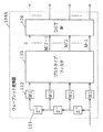
図1は、本発明の実施の形態1による通信装置の受信装置を構成する検波部を示すブロック図である。なお、送信装置の構成は図14の送信装置299の構成と同じである。
【0050】
図1において、101は受信部における検波部、102は受信波形データをウェーブレット変換するウェーブレット変換器、103は受信波形データをヒルベルト変換するヒルベルト変換器、104はウェーブレット変換器102と同一構成でヒルベルト変換器からの出力をウェーブレット変換するウェーブレット変換器、105はウェーブレット変換器104からの出力di(i=0〜M−1とする。Mは複数)の奇数番目の符号を反転する符号変換器、106は符号変換器105からの出力データについてヒルベルト変換器103のリプル特性による振幅変動分を補正するレベル変換器、107はウェーブレット変換器102からの出力を実部(I成分)、レベル変換器106からの出力を虚部(Q成分)として複素データを生成する複素データ生成器である。
【0051】
このように構成された通信装置について、扱うサブキャリアをM本とし、サブキャリア番号が1〜Mまでふられているものとして、その動作を説明する。
【0052】
まず、ウェーブレット変換器102により、受信波形データをウェーブレット変換し、M本のサブキャリア各々に対する同相成分を得る。一方、ヒルベルト変換器103は、受信波形データをヒルベルト変換することで、受信信号に含まれる各周波数成分をπ/2シフトした波形データを生成し、ウェーブレット変換器104によって各サブキャリアの直交成分を得る。このとき、ウェーブレット変換104からの奇数番目の出力は符号が反転した状態で出力されているので、それを符号変換器105によって補正する。さらに、各サブキャリアのデータの振幅がヒルベルト変換器103のリプル特性によって変動しているので、それをレベル変換器106によって補正する。そして、ウェーブレット変換器102、レベル変換器106からの出力をそれぞれ同相成分、直交成分として、複素データ生成器107は複素データを生成する。
【0053】
なお、本実施の形態では同一構成のウェーブレット変換器を2個使用した場合について説明したが、1個のウェーブレット変換器のみでも構成可能である。また高精度なヒルベルト変換器を使用する場合や振幅補正を行う等化器を使用する場合は、レベル変換器、符号変換器は不要となる。
【0054】
以上のように本実施の形態によれば、振幅値のみでなく位相情報も処理の対象とすることができるようになるため、群遅延などによって生じる劣悪な伝送路によって各サブキャリアの同期タイミングずれが生じた場合でもサブキャリア毎に位相回転分を補正することにより、受信性能を向上させることが可能となる。
【0055】
(実施の形態2)
図2は、本発明の実施の形態2による通信装置の受信装置を構成する検波部を示すブロック図である。なお、送信装置の構成は図14の送信装置299の構成と同じである。
【0056】
図2において、108は受信部における検波部、102は受信波形データをウェーブレット変換するウェーブレット変換器、109は受信波形データに対してヒルベルト変換、ウェーブレット変換、奇数番目の符号の反転の処理を一括して行うウェーブレット変換器、107はウェーブレット変換器102からの出力を実部データ(I成分)、ウェーブレット変換器109からの出力を虚部データ(Q成分)として複素データを生成する複素データ生成器である。
【0057】
なお、動作については実施の形態1とほとんど同様であり、異なるのは、実施の形態1において逐次的に処理するヒルベルト変換、ウェーブレット変換、符号反転の処理を、本実施の形態においては、一括処理する点のみである。
【0058】
このような構成にすることにより、実施の形態1に示す構成よりも高速な処理が可能となり、しかも回路構成が簡素化される。
【0059】
(実施の形態3)
図3は、図1、図2の検波部を構成するウェーブレット変換器102を示すブロック図である。また、図4は図3におけるポリフェーズ構成のプロトタイプフィルタの構成を示すブロック図であり、図5は図1のウェーブレット変換器を示すブロック図、図6は図5におけるポリフェーズ構成のプロトタイプフィルタの構成を示すブロック図である。
【0060】
図3において、102は図1あるいは図2に示すウェーブレット変換器、121は受信波形データを1サンプリング時間だけ遅延させる遅延素子、122は受信波形データのサンプリングレートをM分の1にするダウンサンプラ、123はプロトタイプフィルタ、124は高速離散コサイン変換(TYPE4)器である。なお、図3において、遅延素子121はM−1個、ダウンサンプラ122はM個使用する。
【0061】
図4において、123は図3に示すプロトタイプフィルタ、131はプロトタイプフィルタのフィルタ係数をもつ乗算器、132は2入力加算器、133は1シンボル時間(Mサンプリング時間)遅延させる遅延素子である。なお、図4に示すプロトタイプフィルタ123の次数は2Mである。
【0062】
図5において、109Aは図2のウェーブレット変換器109と同じ作用を持つウェーブレット変換器、121は受信波形データを1サンプリング時間だけ遅延させる遅延素子、122は受信波形データのサンプリングレートをM分の1にするダウンサンプラ、125はプロトタイプフィルタ、126は高速離散サイン変換(TYPE4)器である。なお、図5において、遅延素子121はM−1個、ダウンサンプラ122はM個あるものとする。
【0063】
図6において、125は図5に示すプロトタイプフィルタ、131はプロトタイプフィルタのフィルタ係数をもつ乗算器、132は2入力加算器、133は1シンボル時間(Mサンプリング時間)遅延させる遅延素子である。なお、図6に示すプロトタイプフィルタの次数は2Mである。
【0064】
なお、動作については実施の形態2と同様であり、異なるのは、実施の形態2においてFIRフィルタによって実現している部分を、本実施の形態においてはポリフェーズ構成で実現したプロトタイプフィルタと離散コサイン変換あるいは離散サイン変換を用いることによって実現していることにある。
【0065】
また、本実施の形態においては、第1のウェーブレット変換器(ウェーブレット変換器102)および第2のウェーブレット変換器(ウェーブレット変換器109A)を全く別なものとして構成しているが、同一の回路構成を共有することによっても実現可能である。このことは、お互いのプロトタイプフィルタのフィルタ係数が上下反転しているだけであること、離散コサイン変換と離散サイン変換も同様に処理における係数が異なるだけであることから明らかである。
【0066】
以上のような構成にすることにより、FIRフィルタ構成よりもポリフェーズ構成の方が演算量が少ないため、実施の形態2に示す構成よりもさらに高速な処理が可能となる。
【0067】
(実施の形態4)
図7は、図1のウェーブレット変換器(第2のウェーブレット変換器)を示すブロック図である。
【0068】
図7において、109Aは図5のウェーブレット変換器109と同じ作用を持つウェーブレット変換器、121は受信波形データを1サンプリング時間だけ遅延させる遅延素子、122は受信波形データのサンプリングレートをM分の1にするダウンサンプラ、125はプロトタイプフィルタ、127は入力系列をMサンプル単位で時系列反転する時系列反転器、124は高速離散コサイン変換(TYPE4)器、128は入力データの奇数番目の符号を反転する符号変換器である。なお、図5において、遅延素子121はM−1個、ダウンサンプラ122はM個あるものとする。
【0069】
なお、動作については実施の形態3と同様であり、異なるのは、実施の形態3において離散サイン変換器126によって実現している部分を、本実施の形態においては、時系列反転器127と離散コサイン変換器124および符号反転器128によって実現していることにある。また、本実施の形態においては、離散コサイン変換器124の前に時系列反転器127を設置し、離散コサイン変換器124の後に符号反転器128を設置した構成としたが、時系列反転器127と符号反転器128の設置場所を交換した場合においても同様な結果が得られる。
【0070】
上記のような構成にすることにより、実施の形態2に示す構成よりもさらに高速な処理が可能となる。また、実施の形態3において離散コサイン変換器124と離散サイン変換器126を用いていた実現していた部分を離散コサイン変換器124のみで実現可能となるため、回路を共用することができ、回路規模を小さくすることができる。
【0071】
(実施の形態5)
図8は、本発明の実施の形態5による通信装置を構成する受信装置を示すブロック図である。なお、送信装置は図14と同じである。
【0072】
図8において、100は受信装置、110はA/D変換器、108aは図1または図2のいずれかと同様な構成をもつ検波部、120は等化器、130は並直列変換器(P/S変換器)、140は判定器である。
【0073】
このように構成された受信装置について、その動作を説明する。
【0074】
受信装置100において、まず、A/D変換器110により受信信号をディジタル変換し、受信波形データを得る。この受信波形データを検波部108aによって検波し、その出力として、受信信号に含まれる複数のサブキャリアに対する複素情報を得る。次に、等化器120は、検波部108aより得られた複素情報と等化用にあらかじめ割り当てられた既知データとを比較して等化量を求める。そして、実際のデータ伝送シンボル区間において求めた等化量をもって複素情報を等化し、並直列変換器130に供給する。最後に判定器140は等化後の複素情報に基づきデータ判定を行う。これが、受信装置100における一連の動作である。なお、等化器120では、サブキャリアごとに既知信号からの振幅および位相ずれを等化量として求めている。また、伝送路によっては複数タップを使用した適応フィルタ(LMSやRLSなど)を使用することも可能である。
【0075】
上記のような構成により、劣悪な伝送路においても高精度な復調を行うことが可能となる。
【0076】
なお、本実施の形態における等化器120は、下記に示すような形態で使用することも可能である。
【0077】
すなわち、図19は本発明の実施の形態5による通信装置を構成する送信装置を示すブロック図である。
【0078】
また、図19において、200は送信装置、201は連続する数シンボルの間、各サブキャリアに対して同一のデータを発生する同期用データ発生器、210は同期用データに従ってシンボルマッピング(PAM変調)を行うシンボルマッパ、230は逆ウェーブレット変換器、220は逆ウェーブレット変調器からの出力を直列に変換する直並列変換器(S/P変換器)、240は直並列変換器220から出力される送信波形データをアナログ信号に変換するD/A変換器である。
【0079】
このように構成された通信装置について、その動作を図10を用いて説明する。図10はサブキャリアと正弦波周波数との関係を示すグラフである。なお、説明を簡単にするために、使用するウェーブレット変換は8点、すなわちサブキャリア数を8本とする。
【0080】
まず、送信装置200において、同期用データ発生器201は、連続する数シンボルの間、各サブキャリアに対して同一のデータ(例えば1)をシンボルマッパ210に対して出力する。このとき、各サブキャリアに割り当てられるデータは、受信装置100側で既知のデータである。そして、このデータを逆ウェーブレット変換器230によって変換する。このとき、逆ウェーブレット変換器230からの出力は、図10中に示すfnを周波数とした正弦波の合成波となる。そして、この合成波データを直並列変換器220とD/A変換器240とによりアナログ信号に変換して送信する。
【0081】
一方、受信装置100においては、まず、A/D変換器110により受信信号をディジタル変換し、受信波形データを得る。この受信波形データを検波部108によって検波し、その出力として、受信信号に含まれる複数の正弦波に対する複素情報を得る。検波部108は複素データ(複素情報)を等化器120に供給する。等化器120は、検波部108より得られた複素情報を用いて2n−1番目(但し、1≦n≦(M/2−1)、サブキャリア番号を0〜M−1とする)の出力と2n番目の出力を位相を合わせて合成して各サブキャリアに使用する等化係数を精度高く求め、得られた等化係数と等化用にあらかじめ割り当てられた既知データとを使用して等化量を求める。この方式は図10に示すように、2n−1番目と2n番目のサブキャリアが同じ正弦波を使用して等化係数を求めているため実現できる。そして、実際のデータ伝送シンボル区間において求めた等化量をもって複素データを等化し、並直列変換器130に供給する。最後に判定器140は等化後の複素データに基づきデータ判定を行う。
【0082】
上記のような構成により、サブキャリアペア毎に等化係数を求めることができるため、サブキャリア毎に等化係数を求めるよりもさらに高精度に計算することができる。
【0083】
(実施の形態6)
図9(a)は本発明の実施の形態6による通信装置を構成する送信装置を示すブロック図であり、図9(b)は本発明の実施の形態6による通信装置を構成する受信装置を示すブロック図である。
【0084】
図9(b)において、受信装置100、A/D変換器110、検波部108a、等化器120、P/S変換器130、判定器140は図8と同様のものであり、同一符号を付して説明は省略する。図9(b)において、141は1サンプリング時間遅延させる遅延回路、142は複素除算器、143は入力される複素データを累積加算する複素加算器、144は同期ずれ演算器、145は同期タイミング推定回路である。また、図9(a)において、200は送信装置、201は連続する数シンボルの間、各サブキャリアに対して同一のデータを発生する同期用データ発生器、210は同期用データに従ってシンボルマッピング(PAM変調)を行うシンボルマッパ、230は逆ウェーブレット変換器、220は逆ウェーブレット変調器からの出力を直列に変換する直並列変換器(S/P変換器)、240は直並列変換器220から出力される送信波形データをアナログ信号に変換するD/A変換器である。
【0085】
このように構成された通信装置について、その動作を図10を用いて説明する。図10はサブキャリアと正弦波周波数との関係を示すグラフである。なお、説明を簡単にするために、使用するウェーブレット変換は8点、すなわちサブキャリア数を8本とする。
【0086】
まず、送信装置200において、同期用データ発生器201は、連続する数シンボルの間、各サブキャリアに対して同一のデータ(例えば1)をシンボルマッパ210に対して出力する。このとき、各サブキャリアに割り当てられるデータは、受信装置100側で既知のデータである。そして、このデータを逆ウェーブレット変換器230によって変換する。このとき、逆ウェーブレット変換器230からの出力は、図10中に示すfnを周波数とした正弦波の合成波となる。そして、この合成波データを直並列変換器220とD/A変換器240とによりアナログ信号に変換して送信する。
【0087】
一方、受信装置100においては、まず、D/A変換器110により受信信号をディジタル変換し、受信波形データを得る。この受信波形データを検波部108aによって検波し、その出力として、受信信号に含まれる複数の正弦波に対する複素情報を得る。このとき、シンボル同期タイミングが正確に合っていれば、検波部108aからの出力は全て等しい値となるが、同期タイミングが合っていなければ、そのずれの度合いτとサブキャリア周波数fcによって2πfc・τの位相回転を受けた値となっている。次に、遅延素子141と複素除算器142により、隣り合うサブキャリア間の複素除算を行い、複素座標上で位相差を演算する。隣り合うサブキャリア間の周波数間隔fiは全て同じであるから、全てのサブキャリア間位相差(複素値)は等しい値2πfi・τとなる(。しかしながら実際には、伝送路の影響などを受け、2πfi・τよりもばらついた値となる。この各サブキャリア間位相差θcを複素加算器143によって累積加算することにより平均値θmを求め、同期ずれ演算器144において、サブキャリア間間隔fiと平均サブキャリア間位相差θmとから同期ずれ値τm求める。その結果を同期タイミング推定回路145に与えることにより、検波部108aに対し同期タイミングをフィードバックする。ここで、各サブキャリア間位相差から平均サブキャリア間位相差を引いた(θc−θm)(c:サブキャリア間位相差番号)を新たなパラメータとし、同期ずれ演算器144において各サブキャリアにおける同期タイミングと平均同期タイミングとの差τcを求めて、平均同期タイミングからの各サブキャリアの同期タイミングのずれを計算する。このτcを使って各サブキャリアの同期タイミングを微調整する。この微調整が必要な理由としては、各サブキャリアの同期タイミングは伝送路の影響によりずれてしまうので、同期タイミングとしては平均値にあわせる必要がある。しかしながら、平均値では各サブキャリアに対して完全に同期しているといえないので、各サブキャリアの同期タイミングが平均同期タイミングよりどれだけずれているかを求め、そのずれ量に合わせて各サブキャリアの同期タイミングを微調整する。上記のような動作をすることにより、各サブキャリアの同期タイミングずれによる(同期用データの)受信信号と既知信号の信号点のずれを補正することができ、後段にある等化性能を向上させ、結果として受信性能を向上させることができる。
【0088】
同期タイミング確定後、検波部108aは複素データ(複素情報)を等化器120に供給する。等化器120は、検波部108aより得られた複素データと等化用(同期用)にあらかじめ割り当てられた既知データとを比較して等化量を求める。そして、実際のデータ伝送シンボル区間において求めた等化量をもって複素データを等化し、並直列変換器130に供給する。最後に判定器140は等化後の複素データに基づきデータ判定を行う。
【0089】
上記のような構成により、劣悪な伝送路においても高い精度で同期タイミングを推定することが可能となるため、高精度な復調を行うことが可能となる。
【0090】
なお、検波部108aより得られた値は2n−1番目(但し、1≦n≦(M/2−1)、サブキャリア番号を0〜M−1とする)の出力と2n番目の出力を位相を合わせて合成することにより精度の高い位相回転量を求めることができる。この方式は図10に示すように、2n−1番目と2n番目のサブキャリアが同じ正弦波を使用して位相回転量を求めているため実現できる。
【0091】
上記のような構成により、サブキャリアペア毎に同期タイミングはずれによる位相回転量を求めることができるため、サブキャリア毎に位相回転量を求めるよりもさらに高精度に計算することができる。
【0092】
(実施の形態7)
図11は、本発明の実施の形態7による通信装置の受信装置を構成する検波部を示すブロック図である。なお、送信装置は図9(b)と同じである。
【0093】
図11において、151は受信装置における検波部、152は互いに直交するM個の実係数ウェーブレットフィルタで構成されるウェーブレット変換器、153はウェーブレット変換器152からの2n−1番目の出力を複素情報の同相成分(Iチャネル)とし、2n番目の出力を直交成分(Qチャネル)として(但し、1≦n<M/2とする)複素データを生成する複素データ生成器、154は並列に出力される複素データを直列に変換する並直列変換器(P/S変換器)である。
【0094】
このように構成された検波部151について、その動作を図10を用いて説明する。なお、説明を簡単にするため、サブキャリア本数を8として説明する。また、本実施の形態において、受信装置の入力として図10に示す太実線部分(f1、f2、f3)を周波数とする正弦波の合成波が入力されるものとし、それぞれの位相をφ1、φ2、φ3とする。このとき、各正弦波の位相φn(n=1、2、3)は−π〜πの範囲で任意である。
【0095】
まず、検波部151は、受信波形データをウェーブレット変換器152によってウェーブレット変換する。このとき、2n−1番目と2n番目のサブキャリア出力(但し、1≦n≦(M/2−1)、サブキャリア番号は0〜M−1とする)は、それぞれ図10中の各fnを周波数とする正弦波に対するcos(φn)、sin(φn)となる。そして、複素データ生成器153は、cos(φn)を実部データ、sin(φn)を虚部データとして複素データを生成する。最後に並直列変換器154によってシリアル複素データを得る。
【0096】
なお、本実施の形態では合計(M/2−1)個の複素データ生成器153を使用したが、ウェーブレット変換器152からの出力を並直列変換し、そのシリアルデータのうち2n−1番目と2n番目が複素データ生成器153へ入力されるように、タイミング制御を行うことにより、1個の複素データ生成器でも実現可能である。
【0097】
上記のような構成にすることにより、正弦波で構成される受信信号に対してという限定はあるが、少ない演算量(実施の形態3と比較して約半分)で複素情報(複素データ)を得ることが可能となる。
【0098】
(実施の形態8)
図12は、本発明の実施の形態8による通信装置の送信装置を構成する変調器を示すブロック図である。
【0099】
図12において、251は変調器、252はビットデータをシンボルデータに変換し、各シンボルデータに従ってシンボルマッピング(QAM変調)を行うシンボルマッパ、253は逐次入力されたデータを並列に変換する直並列変換器(S/P変換器)、254は入力された複素データを実部と虚部に分解する複素データ分解器、255は逆ウェーブレット変換器である。
【0100】
このように構成された送信装置の変調器251について、その動作を図10を用いて説明する。なお、説明を簡単にするため、サブキャリア本数を8として説明する。また、本実施の形態において、送信装置の出力として図10に示す太実線部分(f1、f2、f3)を周波数とする正弦波の合成波が出力されるものとし、それぞれの位相をφ1、φ2、φ3とする。このとき、各正弦波の位相φn(n=1、2、3)は−π〜πの範囲で任意である。
【0101】
まず、変調器251は、シンボルマッパ252によって送信データ(ビットデータ)をシンボルデータに変換し、各シンボルデータに従ってQAM変調を行い、複素座標上に信号点を配置する。この処理により、(数1)を得る。
【0102】
【数1】

次に、直並列変換器253によってパラレル複素データに変換し、各複素データを複素データ分解器254によって実部データ(cos(φn))と虚部データ(sin(φn))とに分解する。そして、逆ウェーブレット変換器255の2n−1番目の入力に対してcos(φn)を、2n番目に対してsin(φn)を割り当てる(但し、1≦n≦(M/2−1)とする)。すると、逆ウェーブレット変換器255の出力は、図10中の各fnを周波数とし、初期位相φnをもつ正弦波cos(2πfn・t+φn)の合成波となる。
【0104】
なお、本実施の形態では、合計M/2−1個の複素データ分解器を使用したが、1個の複素データ分解器でも実現可能である。
【0105】
上記構成により、シンボルマッパ252で配置された複素座標面の初期位相を各サブキャリア(正確には2n−1と2n番目のサブキャリアによるペア)に対して自由に与えることが可能となるため、各サブキャリアの位相が重ならないようにデータを設定することにより、送信出力の際の瞬時ピーク電圧を抑制することができる。このことにより、送信アンプの仕様を緩和することが可能となる。
【0106】
(実施の形態9)
図13(a)は本発明の実施の形態9による通信装置の送信装置を示すブロック図であり、図13(b)は本発明の実施の形態9による通信装置の受信装置を示すブロック図である。
【0107】
図13(b)において、150は受信装置、110は受信信号をディジタル信号に変換するA/D変換器、151は図11に示す検波部、146は複素平面上で位相を回転させる位相回転器、141は1サンプリング時間遅延させる遅延回路、142は複素除算器、143は入力される複素データを累積加算する複素加算器、144は同期ずれ演算器、145は同期タイミング推定回路である。また図13(a)において、250は送信装置、256は連続する数シンボルの間、各サブキャリアに対して同一のデータを発生する同期用データ発生器、251は図12に示す変調器、240は変調器251により生成された送信波形データをアナログ信号に変換するD/A変換器である。
【0108】
このように構成された通信装置の送信装置250と受信装置150について、その動作を図10を用いて説明する。なお、使用するウェーブレット変換は8点、すなわちサブキャリア数を8本とする。
【0109】
まず、送信装置250において、同期用データ発生器256は、連続する数シンボルの間、各サブキャリアに対して同一のデータを変調器251に対して出力する。このとき、各サブキャリアに割り当てられるデータは、受信装置150側で既知のデータである。そして、この同期用データを変調器251によって変調する。このとき、変調器251からの出力は、図10中に示すfnを周波数とした正弦波の合成波となる。また、各正弦波の位相は入力された同期用データに依存するが、ここでは、位相はφnとする。そして最後に、合成波データをD/A変換240によりアナログ信号に変換して送信する。
【0110】
一方、受信装置150においては、まず、D/A変換器110により受信信号をディジタル変換し、受信波形データを得る。この受信波形データを検波部151によって検波し、その出力として、受信信号に含まれる複数の正弦波それぞれに対する複素信号点情報を得る。ここで得られる複素信号点情報はφnによって位相回転させているため、位相回転器146によりそのφn分だけ複素座標上で位相を戻す。さらに、シンボル同期タイミングが正確に合っていれば、位相回転器146からの出力は全て等しい値となるが、同期タイミングが合っていなければ、そのずれの度合いτとサブキャリア周波数fcによって2πfc・τの位相回転を受けた値となっている。次に、遅延素子141と複素除算器142とにより、隣り合うサブキャリア間の複素除算を行い、複素座標上で位相差を演算する。隣り合うサブキャリア間の周波数間隔fiは全て同じであるから、全てのサブキャリア間位相差(複素値)は等しい値2πfi・τとなる(実際には、伝送路の影響などを受け、2πfi・τよりもばらついた値となる)。このサブキャリア間位相差を複素加算器143によって累積加算することにより平均値φmを求め、同期ずれ演算器144においてサブキャリア間間隔fiと平均サブキャリア間位相差φmから同期ずれ値τを求める。その結果を同期タイミング推定回路145に与えることにより、検波部に対し同期タイミングをフィードバックする。
【0111】
上記のような構成にすることにより、実施の形態6で2つのウェーブレット変換器によって構成された部分を1つのウェーブレット変換器によって実現できるため、回路規模を小さくすることができる。
【0112】
(実施の形態10)
本発明は、信号の送受信を行う通信装置に広く適用されるものであるが、劣悪な伝送路を使用する状況がある電力線通信のシステムに好適である。
【0113】
図20は本発明の実施の形態10による通信装置を構成する送信装置を示すブロック図であり、図21は本発明の実施の形態10による通信装置を構成する受信装置を示すブロック図である。
【0114】
図20において、600は送信部、610はビットデータをシンボルデータに変換しある信号点配置にマッピングするシンボルマッパ、220はシリアルデータをパラレルデータに変換するS/P変換器、620は送信信号を逆変換して変調処理を行う互いに直交する複数M個のフィルタで構成されるフィルタバンクを用いた変調器、240はディジタル信号をアナログ信号に変換するD/A変換器、700は受信部、110はアナログ信号をディジタル信号に変換するA/D変換器、630は受信信号を変換して復調処理を行う互いに直交する複数M個のフィルタで構成されるフィルタバンクを用いた復調器である。
【0115】
次に図20,21を使用して本装置の動作について説明する。
【0116】
送信装置の送信部600において、シンボルマッパ610ではビットデータをシンボルデータに変換してある信号点配置情報に従ってマッピングし、フィルタバンク型変調器620ではシンボルマッパ610において信号点配置された送信信号を逆変換して変調処理を行い、D/A変換器240ではディジタル信号をアナログ信号に変換し、受信装置の検波部700において、A/D変換器110ではアナログ信号をディジタル信号に変換し、フィルタバンク型復調器630では受信信号を変換して復調処理を行う。ここで使用可能なフィルタバンクとしては、時間領域および周波数領域で局在しているような信号を使用したフィルタバンクであり、代表としてWaveletベースのコサイン変調フィルタバンクやFFTベースのPulse Shaping型OFDMなど、があげられる。図にコサイン変調フィルタバンクを用いた場合の振幅スペクトル(フィルタ長4Mの場合)を示す。図ではアマチュア無線帯域と重なるサブキャリアを不使用としてノッチを形成している。このようにフィルタバンクを使用して変復調処理を行うことにより、帯域制限された(Pulse Shapingされた)サブキャリアを使用したマルチキャリア伝送が可能となる。帯域制限型マルチキャリアを電力線通信に使用することにより、狭帯域妨害波やキャリア間干渉などに耐性を持たせることができる。また、各サブキャリアが帯域制限されているので、数本のサブキャリアを不使用とすることにより、鋭いノッチを形成することができる。
【0117】
電力線通信においては、約2M〜30Mまでの帯域を使用可能とする規制緩和が行われようとしている。しかしながらこの帯域は他の既存システムも存在(例えばアマチュア無線や短波放送など)する。電力線通信はこのような他の既存システムに妨害を与えてはならないため、他の既存システムが使用している帯域では信号を送信しないようにしなければならない。通常は、既存システムが使用している帯域に送信しないように別フィルタでノッチフィルタを生成する。米国の電力線通信のアライアンス団体であるHome PlugがリリースしたHome Plug1.0では30dBのノッチフィルタが使用されている。上記から他の既存システムへの妨害抑制目標としては上記の30dB以上が考えられる。
【0118】
本方式はフィルタバンクを使用し各サブキャリアを帯域制限して既存システムの使用帯域と重なるサブキャリアを不使用とすることにより、ノッチフィルタを生成せずに従来方式と同様な動作(他の既存システム使用帯域にノッチを生成:図参照)が可能である。ここでフィルタバンクにおける各フィルタのフィルタ長を(Mを固定して)長くすれば長くするほど、深いノッチが形成されるが、その場合フィルタによる遅延が問題となる(フィルタ遅延とノッチの深さはトレードオフ)。よって、電力線通信においてはフィルタバンクのフィルタ長を4Mに限定することにより、30dB以上のノッチが形成でき、且つフィルタ遅延を抑えることが可能である。
【0119】
(実施の形態11)
図22は本発明の実施の形態11による電力線通信システムを示すブロック図である。図において800は建物、810は電力線、820は電話回線あるいは光回線あるいはCATV回線、700は請求項記載の互いに直交する複数M個のフィルタで構成されるフィルタバンクを用いた通信装置、710はTVやビデオやDVDやDVカメラなどのAV機器、720はルータやADSLやVDSLやメディアコンバータや電話などの通信機器、730はプリンタやFAXやスキャナーなどのドキュメント機器、740はカメラ鍵やインターホンなどのセキュリティ機器、750はパソコン、760はエアコンや冷蔵庫や洗濯機や電子レンジなどの家電機器である。
【0120】
図22を用いて本実施の形態の動作について説明する。各機器は互いに直交する複数M個のフィルタで構成されるフィルタバンクを用いた通信装置を使用して電力線を介してネットワークを構成し、双方向の通信を行う。インターネットへの通信は電力線を介して建物内にあるホームゲートウェイ経由で接続される場合があるし、あるいは電話回線や光回線やCATV回線を媒体として通信行う通信機器を経由して接続される場合があるし、あるいは無線機能を有した通信機器から無線で接続される場合もある。ここで使用している通信装置は、実施の形態10に記載の互いに直交する複数M個のフィルタで構成されるフィルタバンクを変復調処理に用いているため、他の既存システムが使用している帯域に重なるサブキャリアを不使用とすることにより、他の既存システムへの妨害を抑えることができる。またフィルタ長を4Mに限定しているため、30dB以上のノッチの深さを実現し且つフィルタ遅延を抑えている。逆に他の既存システムからの狭帯域妨害の影響を軽減することができる。
【0121】
さらにノッチを生成したい帯域があればその帯域に重なるサブキャリアを不使用とするだけでよいので、容易に各国の規制に柔軟に対応することが可能である。しかも本システム導入後に規制が変更されてもファームのバージョンアップなどにより柔軟に対応できる。なお、建物自体も他のシステムへの輻射軽減に役立つ。
【0122】
なお、以上の全ての実施の形態においてウェーブレット変換を使用し、特に断らない限りウェーブレット変換はコサイン変調フィルタバンクによって行われるものとするとするとしたが、実施の形態の中で特にDCT4やDST4などと限定しているもの以外では、上記の変換方法にとらわれず、Real変換(例えばDCTなど)を変復調に用いたマルチキャリア通信方式全般に適用することができる。
【0123】
以上説明したように本発明に記載の通信装置によれば、ディジタルマルチキャリア復調処理を行う受信装置を有し、実係数ウェーブレットフィルタバンクを用いたディジタルマルチキャリア変復調処理によりデータ伝送を行うマルチキャリア伝送方法を用いた通信装置であって、前記受信装置は検波部を有し、前記検波部は、受信波形データをウェーブレット変換する互いに直交する複数M個の実係数ウェーブレットフィルタで構成される第1のウェーブレット変換器と、前記受信波形データをヒルベルト変換するヒルベルト変換器と、前記ヒルベルト変換器からの出力をウェーブレット変換する第2のウェーブレット変換器と、前記第1のウェーブレット変換器からの出力を複素情報の同相成分とし、前記第2のウェーブレット変換器からの出力を直交成分として複素データを生成する複素データ生成器と、前記第2のウェーブレット変換器からのM個の出力の奇数番目の出力を符号反転する符号変換器とを有することにより、受信装置に到来する実信号のみの時間信号からサブキャリア毎の複素情報を得ることができるので、高精度な復調を行うことができ、また、振幅値のみでなく位相情報も処理の対象とすることができるようになるため、群遅延などによって生じる劣悪な伝送路によって各サブキャリアの同期タイミングずれが生じた場合でもサブキャリア毎に位相回転分を補正して受信性能を向上させることができるという有利な効果が得られる。
【0124】
請求項3に記載の通信装置によれば、ディジタルマルチキャリア復調処理を行う受信装置を有する実係数ウェーブレットフィルタバンクを用いたディジタルマルチキャリア変復調処理によりデータ伝送を行うマルチキャリア伝送方法を用いた通信装置であって、前記受信装置は検波部を有し、前記検波部は、受信波形データをウェーブレット変換する互いに直交する複数M個の実係数ウェーブレットフィルタで構成される第1のウェーブレット変換器と、受信波形データに対してヒルベルト変換、ウェーブレット変換、奇数番目の符号の反転を行うウェーブレットフィルタで構成される第2のウェーブレット変換器と、前記第1のウェーブレット変換器からの出力を複素情報の同相成分とし、前記第2のウェーブレット変換器からの出力を直交成分として複素データを生成する複素データ生成器とを有することにより、受信装置に到来する実信号のみの時間信号からサブキャリア毎の複素情報を得ることができるので、高精度な復調を行うことができ、また、高速な処理を行うことができ、回路構成を簡素化することができるという有利な効果が得られる。
【0126】
請求項4に記載の通信装置によれば、請求項1に記載の通信装置において、第2のウェーブレット変換器は、実係数を有する第2のポリフェーズフィルタで構成された第3のプロトタイプフィルタと、複数M個のダウンサンプラと、M−1個の1サンプル遅延素子と、入力系列の順番をM個単位で反転させる時系列反転器と、高速M点の離散コサイン変換器とを有することにより、第1のウェーブレット変換器の高速M点離散コサイン変換器を共用することができるという有利な効果が得られる。
【0127】
請求項5に記載の通信装置によれば、ディジタルマルチキャリア変調処理を行う送信装置とディジタルマルチキャリア復調処理を行う受信装置とを有し、実係数ウェーブレットフィルタバンクを用いたディジタルマルチキャリア変復調処理によりデータ伝送を行うマルチキャリア伝送方法を用いた通信装置であって、受信装置は、請求項1乃至3のいずれか1に記載の検波部と、検波部から得られる複素情報と等化処理用にあらかじめ割り当てられた等化用既知信号とを用いて等化を行う等化器と、等化器から得られる信号を用いて判定を行う判定器とを有することにより、複素情報と等化用既知信号とを用いて等化を行うことができるので、劣悪な伝送路においても高精度な復調を行うことができるという有利な効果が得られる。
【0128】
請求項6に記載の通信装置によれば、ディジタルマルチキャリア変調処理を行う送信装置とディジタルマルチキャリア復調処理を行う受信装置とを有し、実係数ウェーブレットフィルタバンクを用いたディジタルマルチキャリア変復調処理によりデータ伝送を行うマルチキャリア伝送方法を用いた通信装置であって、送信装置は、連続する数シンボルの間に渡って同一で且つ受信装置で既知の同期用データを発生する同期用データ発生器と、同期用データを逆ウェーブレット変換する逆ウェーブレット変換器とを有し、受信装置は、請求項1乃至5のいずれか1に記載の検波部と、検波部から得られる複素情報と等化処理用にあらかじめ割り当てられた等化用既知信号とを用いて等化を行う等化器と、等化器から得られる信号を用いて判定を行う判定器と、検波部より出力される隣接する複素サブキャリア間の位相差からシンボル同期タイミングを推定する同期推定回路とを有することにより、同じキャリア番号がついた第1のウェーブレットフィルタバンクより得られるサブキャリアと第2のウェーブレットフィルタバンクより得られるサブキャリアとで構成される複素サブキャリア間の位相差からシンボル同期タイミングを推定することができるので、正確且つ高精度の復調を行うことができるという有利な効果が得られる。
【0129】
請求項7に記載の通信装置によれば、ディジタルマルチキャリア変調処理を行う送信装置とディジタルマルチキャリア復調処理を行う受信装置とを有し、実係数ウェーブレットフィルタバンクを用いたディジタルマルチキャリア変復調処理によりデータ伝送を行うマルチキャリア伝送方法を用いた通信装置であって、前記送信装置は、連続する数シンボルの間に渡って同一で且つ前記受信装置で既知の同期用データを発生する同期用データ発生器と、前記同期用データを逆ウェーブレット変換する逆ウェーブレット変換器とを有し、前記受信装置の検波部は、受信波形データをウェーブレット変換する互いに直交する複数M個の実係数ウェーブレットフィルタで構成されるウェーブレット変換器と、前記ウェーブレット変換器からの2n−1番目(nは正の整数)の出力を複素情報の同相成分とし、2n番目の出力を直交成分として(但し、1≦n≦(M/2−1)、サブキャリア番号を0〜M−1とする)複素データを生成する複素データ生成器とを有することにより、受信装置に到来する実信号のみの時間信号からサブキャリア毎の複素情報を得ることができるので、高精度な復調を行うことができ、また、正弦波で構成される受信信号に対してという限定はあるが、少ない演算量で複素データを得ることが可能となるという有利な効果が得られる。
【0130】
請求項8に記載の通信装置によれば、ディジタルマルチキャリア変調処理を行う送信装置とディジタルマルチキャリア復調処理を行う受信装置とを有し、実係数ウェーブレットフィルタバンクを用いたディジタルマルチキャリア変復調処理によりデータ伝送を行うマルチキャリア伝送方法を用いた通信装置であって、送信装置の変調部は、ビットデータをシンボルデータに変換してシンボルデータをM/2個(Mは複数)の複素座標面にマッピングするシンボルマッパと、互いに直交するM個の実係数ウェーブレットフィルタで構成される逆ウェーブレット変換器と、逆ウェーブレット変換器への2n−1番目(nは正の整数)の入力に複素情報の同相成分を、2n番目の入力に複素情報の直交成分を(但し、1≦n≦(M/2−1)、サブキャリア番号を0〜M−1とする)供給するように複素データを実部と虚部に分解する複素データ分解器とを有することにより、信号点配置器(シンボルマッパ)において生成されたM/2個の複素座標面の初期位相を任意に与えることができるという有利な効果が得られる。
【0131】
請求項10に記載の通信装置によれば、ディジタルマルチキャリア変調処理を行う送信装置とディジタルマルチキャリア復調処理を行う受信装置とを有し、実係数ウェーブレットフィルタバンクを用いたディジタルマルチキャリア変復調処理によりデータ伝送を行うマルチキャリア伝送方法を用いた通信装置であって、送信装置は、連続する数シンボルの間に渡って同一で且つ受信装置で既知の同期用データを発生する同期用データ発生器と、同期用データを用いて変調を行う変調部とを有し、受信装置は、請求項7記載の検波部と、隣接する複素サブキャリア間の位相差からシンボル同期タイミングを推定する同期タイミング推定回路とを有することにより、ウェーブレット変換器を1つにすることができるので、受信装置の規模を小さくすることができるという有利な効果が得られる。
【0132】
また、本願の通信装置によれば、伝送路として電力線を用い、ディジタルマルチキャリア変調処理を行う送信装置とディジタルマルチキャリア復調処理を行う受信装置とを有し、変復調処理部分に複数のフィルタから構成されるフィルタバンクを用いる通信装置であって、前記送信装置の送信部は、ビットデータをシンボルデータに変換してある信号点配置情報に従ってマッピングするシンボルマッパと、前記シンボルマッパにおいて信号点配置された送信信号を逆変換して変調処理を行う互いに直交する複数M個のフィルタで構成されるフィルタバンクを用いた変調器とを有し、前記受信装置の検波部は、受信信号を変換して復調処理を行う互いに直交する複数M個のフィルタで構成されるフィルタバンクを有することにより、帯域制限された(Pulse Shapingされた)サブキャリアを使用したマルチキャリア伝送が可能となる。帯域制限型マルチキャリアを電力線通信に使用することにより、狭帯域妨害波やキャリア間干渉などに耐性を持たせることができる。また、各サブキャリアが帯域制限されているので、数本のサブキャリアを不使用とすることにより、鋭いノッチを形成することができる。
【0133】
電力線通信においては、約2M〜30Mまでの帯域を使用可能とする規制緩和が行われようとしている。しかしながらこの帯域は他の既存システムも存在(例えばアマチュア無線や短波放送など)する。電力線通信はこのような他の既存システムに妨害を与えてはならないため、他の既存システムが使用している帯域では信号を送信しないようにしなければならない。通常は、既存システムが使用している帯域に送信しないように別フィルタでノッチフィルタを生成する。米国の電力線通信のアライアンス団体であるHome PlugがリリースしたHome Plug1.0では30dBのノッチフィルタが使用されている。上記から他の既存システムへの妨害抑制目標としては上記の30dB以上が考えられる。
【0134】
本方式はフィルタバンクを使用し各サブキャリアを帯域制限して既存システムの使用帯域と重なるサブキャリアを不使用とすることにより、ノッチフィルタを生成せずに従来方式と同様な動作が可能である。
【図面の簡単な説明】
【図1】本発明の実施の形態1による通信装置の受信装置を構成する検波部を示すブロック図
【図2】本発明の実施の形態2による通信装置の受信装置を構成する検波部を示すブロック図
【図3】図1、図2の検波部を構成するウェーブレット変換器を示すブロック図
【図4】図3におけるポリフェーズ構成のプロトタイプフィルタの構成を示すブロック図
【図5】図1のウェーブレット変換器を示すブロック図
【図6】図5におけるポリフェーズ構成のプロトタイプフィルタの構成を示すブロック図
【図7】図1のウェーブレット変換器(第2のウェーブレット変換器)を示すブロック図
【図8】本発明の実施の形態5による通信装置を構成する受信装置を示すブロック図
【図9】(a)本発明の実施の形態6による通信装置を構成する送信装置を示すブロック図
(b)本発明の実施の形態6による通信装置を構成する受信装置を示すブロック図
【図10】サブキャリアと正弦波周波数との関係を示すグラフ
【図11】本発明の実施の形態7による通信装置の受信装置を構成する検波部を示すブロック図
【図12】本発明の実施の形態8による通信装置の送信装置を構成する変調器を示すブロック図
【図13】(a)本発明の実施の形態9による通信装置の送信装置を示すブロック図
(b)本発明の実施の形態9による通信装置の受信装置を示すブロック図
【図14】DWMC伝送方法を採用した場合の送信装置および受信装置から成る従来の通信装置を示すブロック図
【図15】ウェーブレット波形の例を示す波形図
【図16】DWMC伝送方法における送信波形の例を示す波形図
【図17】DWMC伝送方法における送信スペクトルの例を示すスペクトル図
【図18】DWMC伝送方法における送信フレームの構成例を示すフレーム図
【図19】本発明の実施の形態5による通信装置を構成する送信装置を示すブロック図
【図20】本発明の実施の形態10による通信装置を構成する送信装置を示すブロック図
【図21】本発明の実施の形態10による通信装置を構成する受信装置を示すブロック図
【図22】本発明の実施の形態11による電力線通信システムを示すブロック図
【符号の説明】
100、150 受信装置
101、108、108a、151 検波部
102、104、109、109A、152 ウェーブレット変換器
103 ヒルベルト変換器
105 符号変換器
106 レベル変換器
107、153 複素データ生成器
110 A/D変換器
120 等化器
121、133、141 遅延素子
122 ダウンサンプラ
123、125 プロトタイプフィルタ
124 離散コサイン変換器
126 離散サイン変換器
127 時系列反転器
128 符号反転器
130、154 並直列変換器(P/S変換器)
131 乗算器
132 加算器
140 判定器
142 複素除算器
143 複素加算器
144 同期ずれ演算器
145 同期タイミング推定回路
146 位相回転器
200、250 送信装置
201、256 同期用データ発生器
210 シンボルマッパ(PAM)
220、253 直並列変換器(S/P変換器)
230、255 逆ウェーブレット変換器
240 D/A変換器
251 変調器
252 シンボルマッパ(QAM)
254 複素データ分解器[0001]
BACKGROUND OF THE INVENTION
The present invention relates to a communication apparatus using a multicarrier transmission method (Digital Wavelet Multi Carrier transmission method, hereinafter referred to as “DWMC transmission method”) that performs data transmission by digital modulation / demodulation processing using a real coefficient wavelet filter bank.
[0002]
[Prior art]
A transmission method by digital modulation / demodulation processing using a real coefficient wavelet filter bank is a kind of multicarrier modulation method, and a transmission signal is generated by synthesizing a plurality of digital modulation waves using a real coefficient filter bank. PAM (Pulse Amplitude Modulation) is used as the modulation method of each carrier.
[0003]
Data transmission by the DWMC transmission method will be described with reference to FIGS. 15 is a waveform diagram showing an example of a wavelet waveform, FIG. 16 is a waveform diagram showing an example of a transmission waveform in the DWMC transmission method, FIG. 17 is a spectrum diagram showing an example of a transmission spectrum in the DWMC transmission method, and FIG. It is a frame diagram which shows the structural example of the transmission frame in a transmission method.
[0004]
In data transmission by the DWMC transmission method, as shown in FIG. 15, the impulse response of each subcarrier is transmitted while overlapping in each subcarrier. As shown in FIG. 16, each transmission symbol has a time waveform in which the impulse response of each subcarrier is synthesized. FIG. 17 shows an example of an amplitude spectrum. In the DWMC transmission method, several tens to several hundreds of transmission symbols in FIG. 16 are collected to form one transmission frame. A configuration example of the DWMC transmission frame is shown in FIG. The DWMC transmission frame includes a frame synchronization symbol and an equalization symbol in addition to the information data transmission symbol.
[0005]
FIG. 14 is a block diagram showing a conventional communication apparatus including a
[0006]
In FIG. 14, 110 is an A / D converter, 120 is a wavelet converter, 130 is a P / S converter that converts parallel data into serial data, 140 is a determiner that determines a received signal, and 210 is bit data. A symbol mapper that converts symbol data and performs symbol mapping, 220 is an S / P converter that converts serial data into parallel data, 230 is an inverse wavelet converter, and 240 is a D / A converter.
[0007]
The operation of the communication apparatus configured as described above will be described.
[0008]
First, in
[0009]
In receiving
[0010]
By the way, in communication, amplitude distortion and phase distortion are generated due to the influence of impedance variation of the transmission path, multipath, etc., so it is more convenient to handle both amplitude and phase parameters, that is, complex information. On the other hand, since the conventional DWMC transmission method can only handle amplitude information, distortion cannot be corrected depending on the state of the transmission path, and transmission efficiency is greatly suppressed (for example, (Refer
[0011]
[Non-Patent Document 1]
Hitoshi Kiya, “Digital Signal Processing Series 14 Multirate Signal Processing”, published by Shosodo, October 6, 1995, P186-190
[0012]
[Problems to be solved by the invention]
As described above, the communication device using the transmission method using the conventional real coefficient filter bank has a problem that only the amplitude information can be handled as the transmission data, and the processing that handles the complex information cannot be performed by the receiving device. It was.
[0013]
This communication device is required to use a DWMC transmission method that can handle complex information.
[0014]
An object of the present invention is to provide a communication apparatus using a DWMC transmission method capable of handling complex information in order to satisfy this requirement.
[0015]
[Means for Solving the Problems]
In order to solve this problem, a communication apparatus of the present invention includes a receiving apparatus that performs digital multicarrier demodulation processing, and a multicarrier transmission method that performs data transmission by digital multicarrier modulation / demodulation processing using a real coefficient wavelet filter bank. The reception device includes a detection unit, and the detection unit includes a first wavelet transform composed of a plurality of M real coefficient wavelet filters orthogonal to each other for wavelet transform of received waveform data. , A Hilbert transformer that performs Hilbert transform on the received waveform data, a second wavelet transformer that performs wavelet transform on the output from the Hilbert transformer, and an in-phase complex information output from the first wavelet transformer Component and output from the second wavelet transformer And a structure having a complex data generator for generating complex data as orthogonal components.
[0016]
Thereby, a communication apparatus using the DWMC transmission method that can handle complex information is obtained.
[0017]
DETAILED DESCRIPTION OF THE INVENTION
The communication apparatus according to
[0018]
With this configuration, complex information for each subcarrier can be obtained from the time signal of only the real signal arriving at the receiving device, so that highly accurate demodulation can be performed, and not only the amplitude value but also the phase information is processed. As a result, even if a subcarrier synchronization timing shift occurs due to a poor transmission path caused by group delay or the like, the phase rotation is corrected for each subcarrier to improve reception performance. It has the effect of being able to.
[0021]
Claim2The communication device according to
[0022]
With this configuration, complex information for each subcarrier can be obtained from the time signal of only the real signal arriving at the receiving device, so that highly accurate demodulation can be performed, and not only the amplitude value but also the phase information is processed. As a result, even if a subcarrier synchronization timing shift occurs due to a poor transmission path caused by group delay or the like, the phase rotation is corrected for each subcarrier to improve reception performance. It has the effect of being able to.
[0023]
Claim3The communication device described in 1 is a communication device using a multicarrier transmission method that performs data transmission by digital multicarrier modulation / demodulation processing using a real coefficient wavelet filter bank having a reception device that performs digital multicarrier demodulation processing. The apparatus includes a detection unit, and the detection unit includes a first wavelet transformer including a plurality of M real coefficient wavelet filters orthogonal to each other for wavelet transforming received waveform data, and Hilbert transform for the received waveform data. , Wavelet transform, a second wavelet transformer configured with a wavelet filter that inverts odd-numbered codes, and an output from the first wavelet transformer as an in-phase component of complex information, and from the second wavelet transformer Generates complex data with the output of In which it was decided to have a complex data generator.
[0024]
With this configuration, since complex information for each subcarrier can be obtained from a time signal of only a real signal arriving at the receiving device, high-precision demodulation can be performed, and in the communication device according to
[0027]
Claim4The communication device according to
[0028]
With this configuration, the high-speed M-point discrete cosine transformer of the first wavelet transformer can be shared.
[0029]
Claim5The communication device described in 1 is a communication device using a multicarrier transmission method that has a receiving device that performs digital multicarrier demodulation processing and performs data transmission by digital multicarrier modulation / demodulation processing using a real coefficient wavelet filter bank. The receiving device is defined in
[0030]
With this configuration, it is possible to perform equalization using complex information and a known signal for equalization, so that it is possible to perform highly accurate demodulation even in a poor transmission path.
[0031]
Claim6The communication device described in 1 includes a transmission device that performs digital multicarrier modulation processing and a reception device that performs digital multicarrier demodulation processing. The communication device performs data transmission by digital multicarrier modulation / demodulation processing using a real coefficient wavelet filter bank. A communication apparatus using a carrier transmission method, wherein a transmission apparatus includes a synchronization data generator that generates synchronization data that is the same over a number of consecutive symbols and is known in a reception apparatus, and synchronization data. An inverse wavelet transformer that performs inverse wavelet transformation, and the receiving device includes:5An equalizer that performs equalization using the detection unit according to any one of the above, a complex information obtained from the detection unit, and a known signal for equalization that is allocated in advance for equalization processing, and an equalizer A determination unit that performs determination using the obtained signal and a synchronization estimation circuit that estimates the symbol synchronization timing from the phase difference between adjacent complex subcarriers output from the detection unit are provided.
[0032]
With this configuration, a phase difference between complex subcarriers in a complex subcarrier composed of a subcarrier obtained from the first wavelet filter bank with the same carrier number and a subcarrier obtained from the second wavelet filter bank. Since the symbol synchronization timing can be estimated from the above, it has an effect that accurate and highly accurate demodulation can be performed.
[0033]
Claim7The communication device described in 1 includes a transmission device that performs digital multicarrier modulation processing and a reception device that performs digital multicarrier demodulation processing. The communication device performs data transmission by digital multicarrier modulation / demodulation processing using a real coefficient wavelet filter bank. A communication apparatus using a carrier transmission method, wherein a transmission apparatus includes a synchronization data generator that generates synchronization data that is the same over a number of consecutive symbols and is known in a reception apparatus, and synchronization data. A wavelet transformer including a plurality of M real coefficient wavelet filters orthogonal to each other for wavelet transforming received waveform data, and a wavelet transformer. 2n-1th output (where n is a positive integer) A complex data generator for generating complex data with the 2n-th output as a quadrature component (where 1 ≦ n ≦ (M / 2-1) and
[0034]
With this configuration, it is possible to obtain complex information for each subcarrier from the time signal of only the real signal arriving at the receiving device, so that highly accurate demodulation can be performed, and the received signal configured with a sine wave On the other hand, although there is a limitation, complex data can be obtained with a small amount of calculation.
[0035]
Claim8The communication device described in 1 includes a transmission device that performs digital multicarrier modulation processing and a reception device that performs digital multicarrier demodulation processing. The communication device performs data transmission by digital multicarrier modulation / demodulation processing using a real coefficient wavelet filter bank. A communication apparatus using a carrier transmission method, wherein a modulation unit of a transmission apparatus converts a bit data into symbol data and maps the symbol data onto M / 2 (M is a plurality) complex coordinate planes; The inverse wavelet transformer composed of M real coefficient wavelet filters orthogonal to each other, and the 2n-1th input (n is a positive integer) to the inverse wavelet transformer, the in-phase component of the complex information is 2nth The orthogonal component of the complex information is input to the input (where 1 ≦ n ≦ (M / 2-1) and the subcarrier number is And ~M-1) in which the complex data to supply was to have a real part and an imaginary part in decomposing complex data decomposer.
[0036]
With this configuration, the initial phase of M / 2 complex coordinate planes generated in the signal point locator (symbol mapper) can be arbitrarily given.
[0037]
Claim9The communication device according to
[0038]
With this configuration, the initial phase of M / 2 complex coordinate planes generated in the signal point locator (symbol mapper) can be given.
[0039]
Claim10The communication device described in 1 includes a transmission device that performs digital multicarrier modulation processing and a reception device that performs digital multicarrier demodulation processing. The communication device performs data transmission by digital multicarrier modulation / demodulation processing using a real coefficient wavelet filter bank. A communication apparatus using a carrier transmission method, wherein a transmission apparatus includes a synchronization data generator that generates synchronization data that is the same over a number of consecutive symbols and is known in a reception apparatus, and synchronization data. And a modulation unit that performs modulation using the receiver,7And a synchronization timing estimation circuit that estimates a symbol synchronization timing from a phase difference between adjacent complex subcarriers.
[0040]
With this configuration, since one wavelet transformer can be provided, there is an effect that the size of the receiving apparatus can be reduced.
[0041]
Claim11In the communication device described in 1), the reception device uses the complex information obtained from the detection unit to be 2n−1th (where 1 ≦ n ≦ (M / 2-1), and the subcarrier number is 0 to M−1. And the 2n-th output to obtain an equalization coefficient to be used for each subcarrier, and a determination unit that performs determination using a signal obtained from the equalizer. Claims6It is a communication apparatus as described in above.
[0042]
With this configuration, since the equalization coefficient can be obtained for each complex subcarrier pair using each complex subcarrier pair, the accuracy in obtaining each equalization coefficient can be improved.
[0043]
In addition,The communication apparatus uses a power line as a transmission line, includes a transmission apparatus that performs digital multicarrier modulation processing and a reception apparatus that performs digital multicarrier demodulation processing, and uses a filter bank including a plurality of filters in a modulation / demodulation processing portion. A communication device, wherein the transmission unit of the transmission device converts bit data into symbol data.pointThere is a symbol mapper that maps according to the arrangement information, and a modulator that uses a filter bank composed of a plurality of M filters that are orthogonal to each other and performs modulation processing by inversely transforming the transmission signal arranged at the signal point in the symbol mapper. The detection unit of the reception device is a communication device characterized by having a filter bank composed of a plurality of M filters orthogonal to each other that convert a received signal and perform demodulation processing.
[0044]
With this configuration, in power line communication, other existing systems should not be disturbed, so that signals are not transmitted in the band used by other existing systems. Normally, a notch filter is generated by another filter so as not to transmit to the existing system use band. In Home Plug 1.0 released by Home Plug, an alliance organization of power line communications in the United States, a 30 dB notch filter is used. The above 30 dB is appropriate as a target for suppressing interference from the above to other existing systems.
[0045]
By configuring as described above, this method does not generate a notch filter, and does not use a subcarrier that overlaps the band used in the existing system, thereby operating similarly to the conventional method (in other existing system band used). (Notch can be generated).
[0046]
In addition,The communication device is characterized in that the filter length of the filter of the transmission device and the reception device is 4M.Communication deviceIt is.
[0047]
With the above configuration, generally, the longer the filter length of each filter in the filter bank, the deeper the notch is formed. In that case, the delay due to the filter becomes a problem (filter delay and The notch depth is a trade-off). Therefore, in power line communication, by limiting the filter length of the filter to 4M, a 30 dB notch can be formed and the filter delay can be suppressed.
In addition,The communication device is a receiving device that receives a plurality of carriers and demodulates the received plurality of carriers, and generates a real part data corresponding to each of the plurality of carriers by wavelet transforming the plurality of carriers. A data generation unit, an imaginary part data generation unit that generates imaginary part data having a phase orthogonal to at least one carrier corresponding to the real part data, and the real part data as an in-phase componentandA complex data generator that generates complex data using the imaginary part data as an orthogonal component.
With this configuration, complex information for each subcarrier can be obtained from the time signal of only the real signal arriving at the receiving device, so that highly accurate demodulation can be performed, and not only the amplitude value but also the phase information is processed. As a result, even if a subcarrier synchronization timing shift occurs due to a poor transmission path caused by group delay or the like, the phase rotation is corrected for each subcarrier to improve reception performance. It has the effect of being able to.
[0048]
Hereinafter, embodiments of the present invention will be described with reference to FIGS. In the following embodiments, wavelet transformation is performed by a cosine modulation filter bank unless otherwise specified.
[0049]
(Embodiment 1)
FIG. 1 is a block diagram showing a detection unit constituting the receiving device of the communication device according to
[0050]
In FIG. 1,
[0051]
The operation of the communication apparatus configured as described above will be described on the assumption that M subcarriers are handled and
[0052]
First, the
[0053]
In this embodiment, the case where two wavelet transformers having the same configuration are used has been described. However, it is possible to configure only one wavelet transformer. Further, when a high-precision Hilbert transformer is used or when an equalizer that performs amplitude correction is used, a level converter and a code converter are not necessary.
[0054]
As described above, according to the present embodiment, not only the amplitude value but also phase information can be processed, so that the synchronization timing shift of each subcarrier is caused by a poor transmission path caused by group delay or the like. Even in the case of occurrence of reception, it is possible to improve reception performance by correcting the phase rotation for each subcarrier.
[0055]
(Embodiment 2)
FIG. 2 is a block diagram showing a detection unit constituting the receiving device of the communication device according to
[0056]
In FIG. 2,
[0057]
The operation is almost the same as that of the first embodiment, except that the Hilbert transform, wavelet transform, and sign inversion processing that are sequentially processed in the first embodiment are collectively processed in the present embodiment. It is only a point to do.
[0058]
With such a configuration, it is possible to perform processing at a higher speed than the configuration shown in
[0059]
(Embodiment 3)
FIG. 3 is a block diagram showing the
[0060]
In FIG. 3,
[0061]
In FIG. 4, 123 is a prototype filter shown in FIG. 3, 131 is a multiplier having filter coefficients of the prototype filter, 132 is a two-input adder, and 133 is a delay element that delays one symbol time (M sampling time). Note that the order of the
[0062]
In FIG. 5, 109A is a wavelet transformer having the same action as the
[0063]
In FIG. 6, 125 is a prototype filter shown in FIG. 5, 131 is a multiplier having filter coefficients of the prototype filter, 132 is a two-input adder, and 133 is a delay element that delays one symbol time (M sampling time). Note that the order of the prototype filter shown in FIG. 6 is 2M.
[0064]
The operation is the same as that of the second embodiment, except that the part realized by the FIR filter in the second embodiment is different from the prototype filter realized by the polyphase configuration in this embodiment and the discrete cosine. This is realized by using transformation or discrete sine transformation.
[0065]
In the present embodiment, the first wavelet transformer (wavelet transformer 102) and the second wavelet transformer (
[0066]
With the configuration as described above, the polyphase configuration has a smaller amount of calculation than the FIR filter configuration, so that higher-speed processing is possible than the configuration shown in the second embodiment.
[0067]
(Embodiment 4)
FIG. 7 is a block diagram showing the wavelet transformer (second wavelet transformer) of FIG.
[0068]
In FIG. 7, 109A is a wavelet transformer having the same action as the
[0069]
The operation is the same as that of the third embodiment. The difference is that the portion realized by the
[0070]
By adopting the above configuration, it is possible to perform processing at a higher speed than the configuration shown in the second embodiment. In addition, since the portion realized using the
[0071]
(Embodiment 5)
FIG. 8 is a block diagram showing a receiving apparatus constituting the communication apparatus according to Embodiment 5 of the present invention. The transmitter is the same as that shown in FIG.
[0072]
In FIG. 8, 100 is a receiving device, 110 is an A / D converter, 108a is a detector having the same configuration as in FIG. 1 or FIG. 2, 120 is an equalizer, 130 is a parallel-serial converter (P /
[0073]
The operation of the receiving apparatus configured as described above will be described.
[0074]
In the receiving
[0075]
With the above configuration, it is possible to perform highly accurate demodulation even in a poor transmission path.
[0076]
The
[0077]
That is, FIG. 19 is a block diagram showing a transmission apparatus constituting the communication apparatus according to Embodiment 5 of the present invention.
[0078]
In FIG. 19, 200 is a transmitter, 201 is a synchronization data generator that generates the same data for each subcarrier for several consecutive symbols, and 210 is symbol mapping (PAM modulation) according to the synchronization data. Symbol mapper for performing the operation, 230 is an inverse wavelet converter, 220 is a serial / parallel converter (S / P converter) that converts the output from the inverse wavelet modulator in series, 240 is a transmission output from the serial /
[0079]
The operation of the communication apparatus configured as described above will be described with reference to FIG. FIG. 10 is a graph showing the relationship between the subcarrier and the sine wave frequency. For simplicity of explanation, the wavelet transform used is 8 points, that is, the number of subcarriers is 8.
[0080]
First, in
[0081]
On the other hand, in the receiving
[0082]
With the configuration as described above, an equalization coefficient can be obtained for each subcarrier pair, and therefore, it can be calculated with higher accuracy than obtaining an equalization coefficient for each subcarrier.
[0083]
(Embodiment 6)
FIG. 9 (a) is a block diagram showing a transmitting apparatus constituting the communication apparatus according to Embodiment 6 of the present invention, and FIG. 9 (b) shows a receiving apparatus constituting the communication apparatus according to Embodiment 6 of the present invention. FIG.
[0084]
In FIG. 9B, the receiving
[0085]
The operation of the communication apparatus configured as described above will be described with reference to FIG. FIG. 10 is a graph showing the relationship between the subcarrier and the sine wave frequency. For simplicity of explanation, the wavelet transform used is 8 points, that is, the number of subcarriers is 8.
[0086]
First, in
[0087]
On the other hand, in the receiving
[0088]
After the synchronization timing is determined, the
[0089]
With the configuration as described above, the synchronization timing can be estimated with high accuracy even in a poor transmission path, so that highly accurate demodulation can be performed.
[0090]
The values obtained from the
[0091]
With the configuration as described above, the phase rotation amount due to the shift of the synchronization timing can be obtained for each subcarrier pair, so that it can be calculated with higher accuracy than the phase rotation amount for each subcarrier.
[0092]
(Embodiment 7)
FIG. 11 is a block diagram showing a detection unit constituting the receiving device of the communication device according to the seventh embodiment of the present invention. The transmitting apparatus is the same as that shown in FIG.
[0093]
In FIG. 11, 151 is a detector in the receiving device, 152 is a wavelet transformer composed of M real coefficient wavelet filters orthogonal to each other, and 153 is the 2n-1th output from the
[0094]
The operation of the
[0095]
First, the
[0096]
In the present embodiment, a total of (M / 2-1) complex data generators 153 are used, but the output from the
[0097]
With the above configuration, although there is a limitation on a reception signal composed of a sine wave, complex information (complex data) can be obtained with a small amount of computation (about half compared with Embodiment 3). Can be obtained.
[0098]
(Embodiment 8)
FIG. 12 is a block diagram showing a modulator constituting the transmission device of the communication device according to Embodiment 8 of the present invention.
[0099]
In FIG. 12, 251 is a modulator, 252 is a symbol mapper that converts bit data into symbol data, and performs symbol mapping (QAM modulation) according to each symbol data, and 253 is a serial-parallel conversion that converts sequentially input data in parallel. (S / P converter) 254 is a complex data decomposer that decomposes input complex data into a real part and an imaginary part, and 255 is an inverse wavelet converter.
[0100]
The operation of the
[0101]
First, the
[0102]
[Expression 1]
Next, the serial /
[0104]
In the present embodiment, a total of M / 2-1 complex data decomposers are used. However, a single complex data decomposer can also be realized.
[0105]
With the above configuration, the initial phase of the complex coordinate plane arranged by the
[0106]
(Embodiment 9)
FIG. 13 (a) is a block diagram showing a transmission device of a communication apparatus according to Embodiment 9 of the present invention, and FIG. 13 (b) is a block diagram showing a reception apparatus of the communication apparatus according to Embodiment 9 of the present invention. is there.
[0107]
In FIG. 13B, 150 is a receiving device, 110 is an A / D converter that converts a received signal into a digital signal, 151 is a detector shown in FIG. 11, and 146 is a phase rotator that rotates a phase on a complex plane. , 141 is a delay circuit that delays one sampling time, 142 is a complex divider, 143 is a complex adder that cumulatively adds input complex data, 144 is a synchronization shift calculator, and 145 is a synchronization timing estimation circuit. In FIG. 13A, 250 is a transmitter, 256 is a synchronization data generator that generates the same data for each subcarrier for several consecutive symbols, 251 is a modulator shown in FIG. Is a D / A converter that converts transmission waveform data generated by the
[0108]
Operations of the
[0109]
First, in
[0110]
On the other hand, in the receiving
[0111]
With the above configuration, the portion configured by the two wavelet transformers in the sixth embodiment can be realized by one wavelet transformer, so that the circuit scale can be reduced.
[0112]
(Embodiment 10)
The present invention is widely applied to communication apparatuses that perform signal transmission / reception, but is suitable for a power line communication system in which a poor transmission path is used.
[0113]
FIG. 20 is a block diagram showing a transmitting apparatus constituting a communication apparatus according to Embodiment 10 of the present invention, and FIG. 21 is a block diagram showing a receiving apparatus constituting the communication apparatus according to Embodiment 10 of the present invention.
[0114]
In FIG. 20, 600 is a transmission unit, 610 is a symbol mapper that converts bit data into symbol data and maps it to a certain signal point arrangement, 220 is an S / P converter that converts serial data into parallel data, and 620 is a transmission signal. Modulator using a filter bank composed of a plurality of M filters orthogonal to each other for inverse conversion, 240 is a D / A converter that converts a digital signal into an analog signal, 700 is a receiver, 110 Is an A / D converter for converting an analog signal into a digital signal, and 630 is a demodulator using a filter bank composed of a plurality of M filters orthogonal to each other for converting a received signal and performing demodulation processing.
[0115]
Next, operation | movement of this apparatus is demonstrated using FIG.
[0116]
In the
[0117]
In power line communication, regulations are being relaxed so that a bandwidth of about 2M to 30M can be used. However, there are other existing systems in this band (for example, amateur radio and short wave broadcasting). Since power line communication must not interfere with such other existing systems, it is necessary not to transmit signals in the band used by other existing systems. Usually, a notch filter is generated with another filter so as not to transmit to a band used by an existing system. In Home Plug 1.0 released by Home Plug, an alliance organization of power line communications in the United States, a 30 dB notch filter is used. The above 30 dB or more can be considered as a target for suppressing interference from the above to other existing systems.
[0118]
This method uses a filter bank to limit the bandwidth of each subcarrier so that the subcarrier that overlaps the bandwidth used by the existing system is not used. It is possible to generate a notch in the system use band (see figure). Here, the longer the filter length of each filter in the filter bank (with M fixed), the deeper the notch is formed. In this case, the delay due to the filter becomes a problem (the filter delay and the depth of the notch). Is a trade-off). Therefore, in power line communication, by limiting the filter length of the filter bank to 4M, a notch of 30 dB or more can be formed, and the filter delay can be suppressed.
[0119]
(Embodiment 11)
FIG. 22 is a block diagram showing a power line communication system according to Embodiment 11 of the present invention. In the figure, 800 is a building, 810 is a power line, 820 is a telephone line, optical line or CATV line, 700 is a communication apparatus using a filter bank comprising a plurality of M filters orthogonal to each other, and 710 is a TV AV equipment such as video, DVD, DV camera, etc., 720 is communication equipment such as router, ADSL, VDSL, media converter and telephone, 730 is document equipment such as printer, FAX and scanner, 740 is security such as camera key and
[0120]
The operation of this embodiment will be described with reference to FIG. Each device configures a network via a power line using a communication device using a filter bank including a plurality of M filters orthogonal to each other, and performs bidirectional communication. Communication to the Internet may be connected via a power gateway to a home gateway in the building, or may be connected via a communication device that communicates using a telephone line, optical line, or CATV line as a medium. In some cases, the communication device having a wireless function may be connected wirelessly. Since the communication apparatus used here uses the filter bank composed of a plurality of M filters orthogonal to each other as described in the tenth embodiment for modulation / demodulation processing, the band used by other existing systems By not using subcarriers that overlap each other, interference with other existing systems can be suppressed. Further, since the filter length is limited to 4M, a notch depth of 30 dB or more is realized and the filter delay is suppressed. Conversely, the influence of narrowband interference from other existing systems can be reduced.
[0121]
Furthermore, if there is a band for which a notch is to be generated, it is only necessary not to use a subcarrier that overlaps the band, so that it is possible to easily respond flexibly to the regulations of each country. Moreover, even if regulations are changed after the introduction of this system, it can be flexibly handled by upgrading the firmware. The building itself is also useful for reducing radiation to other systems.
[0122]
In all of the above embodiments, wavelet transformation is used, and unless otherwise specified, wavelet transformation is assumed to be performed by a cosine modulation filter bank. However, the embodiments are limited to DCT4, DST4, and the like. Other than those described above, the present invention is not limited to the above conversion method, and can be applied to all multicarrier communication systems using Real conversion (for example, DCT) for modulation / demodulation.
[0123]
As described above, according to the communication apparatus described in the present invention, the multi-carrier transmission has a receiving apparatus that performs digital multi-carrier demodulation processing, and performs data transmission by digital multi-carrier modulation / demodulation processing using a real coefficient wavelet filter bank. A communication apparatus using the method, wherein the reception apparatus includes a detection unit, and the detection unit includes a plurality of M real coefficient wavelet filters orthogonal to each other that perform wavelet transform on received waveform data. A wavelet transformer; a Hilbert transformer that transforms the received waveform data into a Hilbert transformer; a second wavelet transformer that wavelet transforms the output from the Hilbert transformer; and the output from the first wavelet transformer as complex information From the second wavelet transformer A complex data generator for generating complex data output as the orthogonal componentA code converter for inverting the sign of odd outputs of the M outputs from the second wavelet transformer;Since it is possible to obtain complex information for each subcarrier from the time signal of only the real signal arriving at the receiving device, it is possible to perform highly accurate demodulation and not only the amplitude value but also the phase information. Since it can be processed, even if there is a synchronization timing shift of each subcarrier due to a poor transmission path caused by group delay etc., the phase rotation is corrected for each subcarrier to improve reception performance The advantageous effect that it can be made is obtained.
[0124]
Claim3Is a communication device using a multicarrier transmission method for performing data transmission by digital multicarrier modulation / demodulation processing using a real coefficient wavelet filter bank having a reception device for performing digital multicarrier demodulation processing. The reception apparatus includes a detection unit, and the detection unit includes a first wavelet transformer configured by a plurality of M real coefficient wavelet filters orthogonal to each other for wavelet transforming received waveform data, and received waveform data. A second wavelet transformer configured with a Hilbert transform, a wavelet transform, and a wavelet filter that inverts an odd-numbered code; and an output from the first wavelet transformer as an in-phase component of complex information, Output from the wavelet transformer of 2 and the orthogonal component The complex data generator for generating complex data, the complex information for each subcarrier can be obtained from the time signal of only the real signal arriving at the receiving device, so that highly accurate demodulation can be performed. In addition, an advantageous effect that high-speed processing can be performed and the circuit configuration can be simplified can be obtained.
[0126]
Claim4In the communication device according to
[0127]
Claim5According to the communication device described in the above, it has a transmission device that performs digital multicarrier modulation processing and a reception device that performs digital multicarrier demodulation processing, and transmits data by digital multicarrier modulation / demodulation processing using a real coefficient wavelet filter bank. A communication device using a multi-carrier transmission method to perform, wherein the receiving device comprises:3An equalizer that performs equalization using the detection unit according to any one of the above, a complex information obtained from the detection unit, and a known signal for equalization that is allocated in advance for equalization processing, and an equalizer Since it is possible to perform equalization using complex information and a known signal for equalization by having a determinator that performs determination using the obtained signal, high-precision demodulation is performed even in a poor transmission path The advantageous effect of being able to be obtained is obtained.
[0128]
Claim6According to the communication device described in the above, it has a transmission device that performs digital multicarrier modulation processing and a reception device that performs digital multicarrier demodulation processing, and transmits data by digital multicarrier modulation / demodulation processing using a real coefficient wavelet filter bank. A communication device using a multicarrier transmission method to perform, wherein the transmission device includes a synchronization data generator that generates synchronization data that is the same over a number of consecutive symbols and that is known in the reception device, and a synchronization data generator And an inverse wavelet transformer that performs inverse wavelet transformation on the data, and the receiving device includes:5An equalizer that performs equalization using the detection unit according to any one of the above, a complex information obtained from the detection unit, and a known signal for equalization that is allocated in advance for equalization processing, and an equalizer Having the same carrier number by having a determinator that performs determination using the obtained signal and a synchronization estimation circuit that estimates the symbol synchronization timing from the phase difference between adjacent complex subcarriers output from the detector Since the symbol synchronization timing can be estimated from the phase difference between the complex subcarriers composed of the subcarrier obtained from the first wavelet filter bank and the subcarrier obtained from the second wavelet filter bank, it is accurate.andAn advantageous effect that high-accuracy demodulation can be performed is obtained.
[0129]
Claim7According to the communication device described in the above, it has a transmission device that performs digital multicarrier modulation processing and a reception device that performs digital multicarrier demodulation processing, and transmits data by digital multicarrier modulation / demodulation processing using a real coefficient wavelet filter bank. A communication device using a multi-carrier transmission method to perform, wherein the transmission device is a synchronization data generator that generates synchronization data that is the same over several consecutive symbols and is known in the reception device; An inverse wavelet transformer that performs inverse wavelet transform on the synchronization data, and the detection unit of the reception device is a wavelet transform composed of a plurality of M real coefficient wavelet filters orthogonal to each other that wavelet transform the received waveform data And 2n-1 th (n A positive integer) output is the in-phase component of complex information, and the 2n-th output is a quadrature component (where 1 ≦ n ≦ (M / 2-1), subcarrier number is 0 to M−1). By having a complex data generator that generates data, complex information for each subcarrier can be obtained from a time signal of only a real signal arriving at a receiving device, so that highly accurate demodulation can be performed. Although there is a limitation on a received signal composed of a sine wave, there is an advantageous effect that complex data can be obtained with a small amount of calculation.
[0130]
Claim8According to the communication device described in the above, it has a transmission device that performs digital multicarrier modulation processing and a reception device that performs digital multicarrier demodulation processing, and transmits data by digital multicarrier modulation / demodulation processing using a real coefficient wavelet filter bank. A communication device using a multicarrier transmission method to perform, wherein a modulation unit of a transmission device converts bit data into symbol data and maps symbol data onto M / 2 (M is a plurality) complex coordinate planes A mapper, an inverse wavelet transformer composed of M real coefficient wavelet filters orthogonal to each other, and an in-phase component of complex information at the 2n-1th input (n is a positive integer) to the inverse wavelet transformer, An orthogonal component of complex information is input to the 2n-th input (where 1 ≦ n ≦ (M / 2-1), subcarrier M / 2 generated in a signal point mapper (symbol mapper) by having a complex data decomposer that decomposes complex data into a real part and an imaginary part so as to be supplied) An advantageous effect is obtained that the initial phase of each complex coordinate plane can be arbitrarily given.
[0131]
Claim10According to the communication device described in the above, it has a transmission device that performs digital multicarrier modulation processing and a reception device that performs digital multicarrier demodulation processing, and transmits data by digital multicarrier modulation / demodulation processing using a real coefficient wavelet filter bank. A communication device using a multicarrier transmission method to perform, wherein the transmission device includes a synchronization data generator that generates synchronization data that is the same over a number of consecutive symbols and that is known in the reception device, and a synchronization data generator And a modulation unit that performs modulation using the data,7By having the described detection unit and the synchronization timing estimation circuit that estimates the symbol synchronization timing from the phase difference between adjacent complex subcarriers, the number of wavelet transformers can be reduced to one. An advantageous effect that it can be reduced is obtained.
[0132]
In addition,According to the communication apparatus, a filter bank that uses a power line as a transmission line, includes a transmission apparatus that performs digital multicarrier modulation processing and a reception apparatus that performs digital multicarrier demodulation processing, and includes a plurality of filters in a modulation / demodulation processing portion A communication device using the transmitter, wherein the transmission unit of the transmission device converts the bit data into symbol data.pointA symbol mapper that maps in accordance with the arrangement information, and a modulator that uses a filter bank composed of a plurality of M filters orthogonal to each other that performs inverse modulation on a transmission signal that is signal point arranged in the symbol mapper and performs modulation processing. And the detection unit of the reception device is band-limited (pulse-shaping) by including a filter bank composed of a plurality of M filters orthogonal to each other that perform demodulation processing by converting a received signal Multicarrier transmission using subcarriers becomes possible. By using the band-limited multi-carrier for power line communication, it is possible to provide resistance to narrow-band jamming waves and inter-carrier interference. Further, since each subcarrier is band-limited, a sharp notch can be formed by not using several subcarriers.
[0133]
In power line communication, regulations are being relaxed so that a bandwidth of about 2M to 30M can be used. However, there are other existing systems in this band (for example, amateur radio and short wave broadcasting). Since power line communication must not interfere with such other existing systems, it is necessary not to transmit signals in the band used by other existing systems. Usually, a notch filter is generated with another filter so as not to transmit to a band used by an existing system. In Home Plug 1.0 released by Home Plug, an alliance organization of power line communications in the United States, a 30 dB notch filter is used. The above 30 dB or more can be considered as a target for suppressing interference from the above to other existing systems.
[0134]
This method can operate in the same way as the conventional method without generating a notch filter by using a filter bank to limit the bandwidth of each subcarrier and not using a subcarrier that overlaps the bandwidth used in the existing system. .
[Brief description of the drawings]
FIG. 1 is a block diagram showing a detection unit constituting a receiving device of a communication device according to a first embodiment of the present invention.
FIG. 2 is a block diagram showing a detection unit constituting a receiving device of a communication device according to a second embodiment of the present invention.
FIG. 3 is a block diagram showing a wavelet transformer constituting the detection unit of FIGS. 1 and 2;
4 is a block diagram showing a configuration of a prototype filter having a polyphase configuration in FIG. 3;
FIG. 5 is a block diagram showing the wavelet transformer of FIG.
6 is a block diagram showing a configuration of a prototype filter having a polyphase configuration in FIG. 5;
7 is a block diagram showing the wavelet transformer (second wavelet transformer) of FIG. 1;
FIG. 8 is a block diagram showing a receiving device constituting a communication device according to a fifth embodiment of the present invention.
FIG. 9 (a) is a block diagram showing a transmission apparatus constituting a communication apparatus according to Embodiment 6 of the present invention.
(B) Block diagram showing a receiving apparatus constituting the communication apparatus according to Embodiment 6 of the present invention.
FIG. 10 is a graph showing the relationship between the subcarrier and the sine wave frequency.
FIG. 11 is a block diagram showing a detection unit constituting a receiving device of a communication device according to a seventh embodiment of the present invention.
FIG. 12 is a block diagram showing a modulator constituting a transmission device of a communication device according to an eighth embodiment of the present invention.
FIG. 13A is a block diagram showing a transmission device of a communication device according to a ninth embodiment of the present invention.
(B) Block diagram showing the receiving device of the communication device according to the ninth embodiment of the present invention.
FIG. 14 is a block diagram showing a conventional communication apparatus including a transmission apparatus and a reception apparatus when the DWMC transmission method is adopted.
FIG. 15 is a waveform diagram showing an example of a wavelet waveform
FIG. 16 is a waveform diagram showing an example of a transmission waveform in the DWMC transmission method
FIG. 17 is a spectrum diagram showing an example of a transmission spectrum in the DWMC transmission method.
FIG. 18 is a frame diagram illustrating a configuration example of a transmission frame in the DWMC transmission method.
FIG. 19 is a block diagram showing a transmission apparatus constituting a communication apparatus according to Embodiment 5 of the present invention.
FIG. 20 is a block diagram showing a transmission apparatus constituting a communication apparatus according to Embodiment 10 of the present invention.
FIG. 21 is a block diagram showing a receiving apparatus constituting a communication apparatus according to Embodiment 10 of the present invention.
FIG. 22 is a block diagram showing a power line communication system according to an eleventh embodiment of the present invention.
[Explanation of symbols]
100, 150 receiver
101, 108, 108a, 151 detector
102, 104, 109, 109A, 152 Wavelet Transformer
103 Hilbert converter
105 Code converter
106 Level converter
107, 153 Complex data generator
110 A / D converter
120 equalizer
121, 133, 141 delay element
122 Downsampler
123, 125 prototype filter
124 Discrete cosine transformer
126 Discrete sine converter
127 time series inverter
128 sign inverter
130, 154 Parallel-serial converter (P / S converter)
131 multiplier
132 Adder
140 Determinator
142 Complex divider
143 Complex adder
144 Synchronization deviation calculator
145 Synchronization timing estimation circuit
146 Phase Rotator
200, 250 Transmitter
201, 256 Data generator for synchronization
210 Symbol Mapper (PAM)
220, 253 serial-parallel converter (S / P converter)
230, 255 Inverse wavelet transformer
240 D / A converter
251 modulator
252 Symbol Mapper (QAM)
254 Complex data decomposer
Claims (11)
前記受信装置は検波部を有し、
前記検波部は、受信波形データをウェーブレット変換する互いに直交する複数M個の実係数ウェーブレットフィルタで構成される第1のウェーブレット変換器と、前記受信波形データをヒルベルト変換するヒルベルト変換器と、前記ヒルベルト変換器からの出力をウェーブレット変換する第2のウェーブレット変換器と、前記第1のウェーブレット変換器からの出力を複素情報の同相成分とし、前記第2のウェーブレット変換器からの出力を直交成分として複素データを生成する複素データ生成器と、
前記第2のウェーブレット変換器からのM個の出力の奇数番目の出力を符号反転する符号変換器とを有することを特徴とする通信装置。 A communication device using a multicarrier transmission method having a receiving device that performs digital multicarrier demodulation processing, and performing data transmission by digital multicarrier modulation / demodulation processing using a real coefficient wavelet filter bank,
The receiving device has a detection unit,
The detection unit includes: a first wavelet transformer configured with a plurality of M real coefficient wavelet filters orthogonal to each other for wavelet transforming received waveform data; a Hilbert transformer for performing Hilbert transform on the received waveform data; and the Hilbert A second wavelet transformer that performs wavelet transform on the output from the converter, and an output from the first wavelet transformer as an in-phase component of complex information, and an output from the second wavelet transformer as a quadrature component A complex data generator for generating data ;
And a code converter for inverting the sign of odd-numbered outputs of M outputs from the second wavelet converter.
前記受信装置は検波部を有し、
前記検波部は、受信波形データをウェーブレット変換する互いに直交する複数M個の実係数ウェーブレットフィルタで構成される第1のウェーブレット変換器と、受信波形データに対してヒルベルト変換、ウェーブレット変換、奇数番目の符号の反転を行うウェーブレットフィルタで構成される第2のウェーブレット変換器と、前記第1のウェーブレット変換器からの出力を複素情報の同相成分とし、前記第2のウェーブレット変換器からの出力を直交成分として複素データを生成する複素データ生成器とを有することを特徴とする通信装置。A communication device using a multicarrier transmission method for performing data transmission by digital multicarrier modulation / demodulation processing using a real coefficient wavelet filter bank having a receiving device for performing digital multicarrier demodulation processing,
The receiving device has a detection unit,
The detection unit includes a first wavelet transformer configured by a plurality of M real coefficient wavelet filters orthogonal to each other for wavelet transforming received waveform data, and Hilbert transform, wavelet transform, odd-numbered received waveform data A second wavelet transformer configured with a wavelet filter that performs code inversion and an output from the first wavelet transformer as an in-phase component of complex information, and an output from the second wavelet transformer as a quadrature component And a complex data generator for generating complex data.
前記受信装置は、請求項1乃至3のいずれか1に記載の検波部と、前記検波部から得られる複素情報と等化処理用にあらかじめ割り当てられた等化用既知信号とを用いて等化を行う等化器と、前記等化器から得られる信号を用いて判定を行う判定器とを有することを特徴とする通信装置。A communication device using a multicarrier transmission method having a receiving device that performs digital multicarrier demodulation processing, and performing data transmission by digital multicarrier modulation / demodulation processing using a real coefficient wavelet filter bank,
The reception apparatus equalizes using the detection unit according to any one of claims 1 to 3 , complex information obtained from the detection unit, and a known signal for equalization allocated in advance for equalization processing. A communication apparatus comprising: an equalizer that performs determination; and a determination unit that performs determination using a signal obtained from the equalizer.
前記送信装置は、連続する数シンボルの間に渡って同一で且つ前記受信装置で既知の同期用データを発生する同期用データ発生器と、前記同期用データを逆ウェーブレット変換する逆ウェーブレット変換器とを有し、
前記受信装置は、請求項1乃至5のいずれか1に記載の検波部と、前記検波部から得られる複素情報と等化処理用にあらかじめ割り当てられた等化用既知信号とを用いて等化を行う等化器と、前記等化器から得られる信号を用いて判定を行う判定器と、前記検波部より出力される隣接する複素サブキャリア間の位相差からシンボル同期タイミングを推定する同期推定回路とを有することを特徴とする通信装置。Communication using a multi-carrier transmission method having a transmission device for performing digital multi-carrier modulation processing and a receiving device for performing digital multi-carrier demodulation processing, and performing data transmission by digital multi-carrier modulation / demodulation processing using a real coefficient wavelet filter bank A device,
The transmission device includes a synchronization data generator that generates synchronization data that is the same over several consecutive symbols and is known by the reception device, and an inverse wavelet transformer that performs inverse wavelet transform on the synchronization data. Have
The reception apparatus equalizes using the detection unit according to any one of claims 1 to 5 , complex information obtained from the detection unit, and a known signal for equalization allocated in advance for equalization processing. Synchronization estimation that estimates symbol synchronization timing from a phase difference between adjacent complex subcarriers output from the detector, and a decision unit that performs determination using a signal obtained from the equalizer And a communication device.
前記送信装置は、連続する数シンボルの間に渡って同一で且つ前記受信装置で既知の同期用データを発生する同期用データ発生器と、前記同期用データを逆ウェーブレット変換する逆ウェーブレット変換器とを有し、
前記受信装置の検波部は、受信波形データをウェーブレット変換する互いに直交する複数M個の実係数ウェーブレットフィルタで構成されるウェーブレット変換器と、前記ウェーブレット変換器からの2n−1番目(nは正の整数)の出力を複素情報の同相成分とし、2n番目の出力を直交成分として(但し、1≦n≦(M/2−1)、サブキャリア番号を0〜M−1とする)複素データを生成する複素データ生成器とを有することを特徴とする通信装置。Communication using a multi-carrier transmission method having a transmission device for performing digital multi-carrier modulation processing and a receiving device for performing digital multi-carrier demodulation processing, and performing data transmission by digital multi-carrier modulation / demodulation processing using a real coefficient wavelet filter bank A device,
The transmission device includes a synchronization data generator that generates synchronization data that is the same over several consecutive symbols and is known by the reception device, and an inverse wavelet transformer that performs inverse wavelet transform on the synchronization data. Have
The detection unit of the receiving device includes a wavelet transformer configured by a plurality of M real coefficient wavelet filters orthogonal to each other for wavelet transforming received waveform data, and 2n-1 th (n is a positive value) from the wavelet transformer. (Integer) output is in-phase component of complex information, 2n-th output is quadrature component (where 1 ≦ n ≦ (M / 2-1), subcarrier number is 0 to M−1) And a complex data generator for generating the communication device.
前記送信装置の変調部は、ビットデータをシンボルデータに変換して前記シンボルデータをM/2個(Mは複数)の複素座標面にマッピングするシンボルマッパと、互いに直交するM個の実係数ウェーブレットフィルタで構成される逆ウェーブレット変換器と、前記逆ウェーブレット変換器への2n−1番目(nは正の整数)の入力に複素情報の同相成分を、2n番目の入力に複素情報の直交成分を(但し、1≦n≦(M/2−1)、サブキャリア番号を0〜M−1とする)供給するように複素データを実部と虚部に分解する複素データ分解器とを有することを特徴とする通信装置。Communication using a multi-carrier transmission method having a transmission device for performing digital multi-carrier modulation processing and a receiving device for performing digital multi-carrier demodulation processing, and performing data transmission by digital multi-carrier modulation / demodulation processing using a real coefficient wavelet filter bank A device,
The modulation unit of the transmission apparatus converts a bit data into symbol data and maps the symbol data to M / 2 (M is a plurality) complex coordinate planes, and M real coefficient wavelets orthogonal to each other. An inverse wavelet transformer composed of filters, an in-phase component of complex information at the 2n-1th input (n is a positive integer) to the inverse wavelet transformer, and an orthogonal component of complex information at the 2nth input (However, 1 ≦ n ≦ (M / 2-1), subcarrier number is set to 0 to M−1) A complex data decomposer that decomposes complex data into a real part and an imaginary part is provided. A communication device characterized by the above.
前記送信装置は、連続する数シンボルの間に渡って同一で且つ前記受信装置で既知の同期用データを発生する同期用データ発生器と、前記同期用データを用いて変調を行う変調部とを有し、
前記受信装置は、請求項7に記載の検波部と、隣接する複素サブキャリア間の位相差からシンボル同期タイミングを推定する同期タイミング推定回路とを有することを特徴とする通信装置。It has a receiving device and performing transmission device and the de-I digital multicarrier demodulation process for the digital multi-carrier modulation process, use a multi-carrier transmission method which performs data transmission by a digital multi-carrier modulation and demodulation processing using a real coefficient wavelet filter bank A communication device,
The transmission device includes a synchronization data generator that generates synchronization data that is the same over several consecutive symbols and that is known in the reception device, and a modulation unit that performs modulation using the synchronization data. Have
8. The communication apparatus comprising: the detection unit according to claim 7; and a synchronization timing estimation circuit that estimates a symbol synchronization timing from a phase difference between adjacent complex subcarriers.
Priority Applications (1)
| Application Number | Priority Date | Filing Date | Title |
|---|---|---|---|
| JP2003193432A JP4292898B2 (en) | 2002-09-25 | 2003-07-08 | Communication device |
Applications Claiming Priority (2)
| Application Number | Priority Date | Filing Date | Title |
|---|---|---|---|
| JP2002278747 | 2002-09-25 | ||
| JP2003193432A JP4292898B2 (en) | 2002-09-25 | 2003-07-08 | Communication device |
Related Child Applications (1)
| Application Number | Title | Priority Date | Filing Date |
|---|---|---|---|
| JP2009014027A Division JP5035259B2 (en) | 2002-09-25 | 2009-01-26 | Communication device |
Publications (3)
| Publication Number | Publication Date |
|---|---|
| JP2004166217A JP2004166217A (en) | 2004-06-10 |
| JP2004166217A5 JP2004166217A5 (en) | 2006-08-17 |
| JP4292898B2 true JP4292898B2 (en) | 2009-07-08 |
Family
ID=32827757
Family Applications (1)
| Application Number | Title | Priority Date | Filing Date |
|---|---|---|---|
| JP2003193432A Expired - Fee Related JP4292898B2 (en) | 2002-09-25 | 2003-07-08 | Communication device |
Country Status (1)
| Country | Link |
|---|---|
| JP (1) | JP4292898B2 (en) |
Families Citing this family (11)
| Publication number | Priority date | Publication date | Assignee | Title |
|---|---|---|---|---|
| DE602004021378D1 (en) * | 2003-06-18 | 2009-07-16 | Panasonic Corp | METHOD AND DEVICE FOR RECEIVING DIGITAL MULTIPLE SIGNAL SIGNALS USING A WAVELET TRANSFORMATION |
| JP4606149B2 (en) * | 2004-12-16 | 2011-01-05 | パナソニック株式会社 | Receiving apparatus and receiving method |
| EP1832007A1 (en) | 2004-12-24 | 2007-09-12 | Matsushita Electric Industrial Co., Ltd. | Line status detection apparatus, communication apparatus, and line status detection method |
| JP4697773B2 (en) * | 2004-12-24 | 2011-06-08 | パナソニック株式会社 | Multi-carrier communication apparatus and multi-carrier communication method |
| JP4555185B2 (en) * | 2005-07-25 | 2010-09-29 | パナソニック株式会社 | Transmitter, receiver and control method thereof |
| JP2007036491A (en) * | 2005-07-25 | 2007-02-08 | Matsushita Electric Ind Co Ltd | Transmitter, receiver, and control method thereof |
| US20090099844A1 (en) * | 2007-10-16 | 2009-04-16 | Qualcomm Incorporated | Efficient implementation of analysis and synthesis filterbanks for mpeg aac and mpeg aac eld encoders/decoders |
| US8111765B2 (en) | 2008-06-12 | 2012-02-07 | Panasonic Corporation | Communication apparatus, communication method, and integrated circuit |
| JP5340199B2 (en) * | 2010-02-18 | 2013-11-13 | 日本放送協会 | Multi-carrier modulation apparatus and demodulation apparatus |
| JP2012147205A (en) * | 2011-01-11 | 2012-08-02 | Nippon Hoso Kyokai <Nhk> | Discrete sine transform circuit, inverse discrete sine transform circuit, combination-use circuit, encoding device, decoding device, and program |
| JP2017152936A (en) * | 2016-02-24 | 2017-08-31 | パナソニックIpマネジメント株式会社 | Communication device and communication method |
-
2003
- 2003-07-08 JP JP2003193432A patent/JP4292898B2/en not_active Expired - Fee Related
Also Published As
| Publication number | Publication date |
|---|---|
| JP2004166217A (en) | 2004-06-10 |
Similar Documents
| Publication | Publication Date | Title |
|---|---|---|
| JP5035259B2 (en) | Communication device | |
| EP2299624B1 (en) | Signaling method in an OFDM multiple access system | |
| EP2315386B1 (en) | OFDM communications methods and apparatus | |
| US7561614B2 (en) | Communication apparatus and communication method using digital wavelet multi carrier transmission system | |
| JP4472692B2 (en) | Receiver and method for digital multicarrier transmission | |
| JP3431785B2 (en) | Orthogonal frequency multiplex modulation signal demodulator | |
| WO2005094028A1 (en) | Periodic training signals | |
| JP4292898B2 (en) | Communication device | |
| EP1639774B1 (en) | Method and apparatus for receiving digital multicarrier signals using a wavelet transform | |
| KR20180052003A (en) | Method and Apparatus for Distortion Compensation of Subcarrier in Orthogonal Frequency Division Multiplexing System | |
| JP4161693B2 (en) | Multicarrier transmission apparatus, multicarrier reception apparatus, and multicarrier communication apparatus | |
| JP2007528624A (en) | Transmitter | |
| JP4390771B2 (en) | Digital radio frequency circuit | |
| JP2003152673A (en) | Orthogonal frequency multiplex modulated signal demodulating method |
Legal Events
| Date | Code | Title | Description |
|---|---|---|---|
| A521 | Written amendment |
Free format text: JAPANESE INTERMEDIATE CODE: A523 Effective date: 20060629 |
|
| A621 | Written request for application examination |
Free format text: JAPANESE INTERMEDIATE CODE: A621 Effective date: 20060629 |
|
| RD01 | Notification of change of attorney |
Free format text: JAPANESE INTERMEDIATE CODE: A7421 Effective date: 20060712 |
|
| A977 | Report on retrieval |
Free format text: JAPANESE INTERMEDIATE CODE: A971007 Effective date: 20081016 |
|
| A131 | Notification of reasons for refusal |
Free format text: JAPANESE INTERMEDIATE CODE: A131 Effective date: 20081125 |
|
| A521 | Written amendment |
Free format text: JAPANESE INTERMEDIATE CODE: A523 Effective date: 20090126 |
|
| TRDD | Decision of grant or rejection written | ||
| A01 | Written decision to grant a patent or to grant a registration (utility model) |
Free format text: JAPANESE INTERMEDIATE CODE: A01 Effective date: 20090317 |
|
| A01 | Written decision to grant a patent or to grant a registration (utility model) |
Free format text: JAPANESE INTERMEDIATE CODE: A01 |
|
| A61 | First payment of annual fees (during grant procedure) |
Free format text: JAPANESE INTERMEDIATE CODE: A61 Effective date: 20090330 |
|
| FPAY | Renewal fee payment (event date is renewal date of database) |
Free format text: PAYMENT UNTIL: 20120417 Year of fee payment: 3 |
|
| FPAY | Renewal fee payment (event date is renewal date of database) |
Free format text: PAYMENT UNTIL: 20120417 Year of fee payment: 3 |
|
| FPAY | Renewal fee payment (event date is renewal date of database) |
Free format text: PAYMENT UNTIL: 20130417 Year of fee payment: 4 |
|
| FPAY | Renewal fee payment (event date is renewal date of database) |
Free format text: PAYMENT UNTIL: 20130417 Year of fee payment: 4 |
|
| FPAY | Renewal fee payment (event date is renewal date of database) |
Free format text: PAYMENT UNTIL: 20140417 Year of fee payment: 5 |
|
| LAPS | Cancellation because of no payment of annual fees |