JP4292425B2 - Gray code counter and display device - Google Patents
Gray code counter and display device Download PDFInfo
- Publication number
- JP4292425B2 JP4292425B2 JP2007075958A JP2007075958A JP4292425B2 JP 4292425 B2 JP4292425 B2 JP 4292425B2 JP 2007075958 A JP2007075958 A JP 2007075958A JP 2007075958 A JP2007075958 A JP 2007075958A JP 4292425 B2 JP4292425 B2 JP 4292425B2
- Authority
- JP
- Japan
- Prior art keywords
- gray code
- bit
- circuit
- output
- value
- Prior art date
- Legal status (The legal status is an assumption and is not a legal conclusion. Google has not performed a legal analysis and makes no representation as to the accuracy of the status listed.)
- Active
Links
- 230000003111 delayed effect Effects 0.000 claims description 9
- 230000001934 delay Effects 0.000 claims description 5
- 239000004973 liquid crystal related substance Substances 0.000 description 11
- 238000010586 diagram Methods 0.000 description 6
- 239000011521 glass Substances 0.000 description 1
- 230000000873 masking effect Effects 0.000 description 1
- 238000000034 method Methods 0.000 description 1
- 229910021420 polycrystalline silicon Inorganic materials 0.000 description 1
- 229920005591 polysilicon Polymers 0.000 description 1
- 230000000630 rising effect Effects 0.000 description 1
- 239000004065 semiconductor Substances 0.000 description 1
- 238000004904 shortening Methods 0.000 description 1
- 239000000758 substrate Substances 0.000 description 1
Images
Landscapes
- Control Of Indicators Other Than Cathode Ray Tubes (AREA)
Description
本発明は、グレイコードカウンタと、グレイコードカウンタを備えた表示装置に関する。 The present invention relates to a gray code counter and a display device including the gray code counter.
従来より、クロックを計数し、その計数値に応じてグレイコードを出力するグレイコードカウンタが知られている。グレイコードは、1つのビットの値のみが「0」から「1」に、又は「1」から「0」に変化するコードである。グレイコードカウンタは通常のカウンタに比して、低消費電力であり、カウントエラーを低減することができる。グレイコードカウンタについては、特許文献1、2に開示されている。
しかしながら、従来のグレイコードカウンタにおいては、グレイコードの生成回路が複雑で、信号の遅延時間を決定するクリティカルパスの遅延時間が長いため、高速動作ができないという問題があった。 However, the conventional gray code counter has a problem that the gray code generation circuit is complicated and the delay time of the critical path for determining the signal delay time is long, so that the high speed operation cannot be performed.
本発明のグレイコードカウンタは、グレイコードを生成するグレイコードカウンタにおいて、第nビットのグレイコードの1つ下位ビットである第(n−1)ビットのグレイコードのクロックを2分周する分周回路と、前記分周回路の出力を第(n−2)ビット以下のグレイコードに基づいて遅延する遅延回路と、前記遅延回路の出力をクロックに応じて保持し、かつ遅延して、第nビットのグレイコードを出力する順序回路と、を備えることを特徴とする。 A gray code counter according to the present invention is a gray code counter that generates a gray code, and divides a clock of a (n−1) -th bit gray code that is one lower bit of the n-th bit gray code by two. A delay circuit that delays the output of the frequency dividing circuit based on a gray code of (n-2) th bit or less, and holds and delays the output of the delay circuit according to the clock, And a sequential circuit that outputs a gray code of bits.
また、本発明の表示装置は、上記のグレイコードカウンタを備えることを特徴とする。 In addition, a display device of the present invention includes the gray code counter described above.
本発明によれば、クリティカルパスの遅延時間を短縮し、高速動作が可能なグレイコードカウンタを提供することができる。また、本発明のグレイコードカウンタを表示装置に用いることにより、表示装置の高速動作が可能になる。 According to the present invention, it is possible to provide a gray code counter capable of shortening a critical path delay time and capable of high-speed operation. Further, by using the gray code counter of the present invention for a display device, the display device can be operated at high speed.
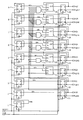
本発明の実施の形態について図面を参照しながら説明する。図1は本発明の実施の形態による8ビットのグレイコードカウンタの回路図である。このグレイコードカウンタは、リセット端子R付きのD型フリップフロップ1〜9(以下、RDFFという)、AND回路11〜15、選択回路21〜26、リセット端子R付きのD型フリップフロップ31〜38(以下、RDFFという)から構成され、8個のRDFF31〜38の出力端子QからそれぞれグレイコードQ0〜Q7(Q0が第1ビット、Q7が第8ビットに当たる)が出力される。
Embodiments of the present invention will be described with reference to the drawings. FIG. 1 is a circuit diagram of an 8-bit Gray code counter according to an embodiment of the present invention. The Gray code counter includes D-type flip-
RDFF1〜9は、その反転出力端子/Qからの反転出力信号がデータ入力端子Dに帰還入力されて、クロック入力端子Cに入力されるクロックを2分周する分周回路であり、それぞれリセット信号RESETによりリセットされる。RDFF1は、クロックCLKを2分周して、出力端子Qから基準クロックQorgを出力する。RDFF2はこの基準クロックQorgをさらに2分周して出力端子Qから出力する。RDFF3〜RDFF9は、それぞれ1ビット下位のグレイコードQ0〜Q6のクロックを2分周してそれぞれの出力端子Qから出力する。
The
選択回路21〜26は、グレイコードの第3ビット〜第8ビットに対応して設けられ、選択信号入力端子SELに入力される選択信号が「0」のとき、第1入力端子IN1に入力された信号を出力端子OUTから出力し、選択信号入力端子SELに入力される選択信号が「1」のとき、第2入力端子IN2に入力された信号を出力端子OUTから出力する回路である。選択回路21〜26は簡単なスイッチング回路で作成することができる。選択回路21〜26の第1入力端子IN1には対応するビットのグレイコードQ2〜Q7が入力され、第2入力端子IN2には対応するビットのRDFF4〜9の出力端子Qから出力される出力信号Q2O〜Q7Oが入力される。
The
上記選択信号は、選択回路21については、第1ビットのグレイコードQ0の反転信号QN0であり、選択回路22〜26については、それぞれAND回路(論理積回路)11〜15で作成される。AND回路11〜15は、第4ビット〜第8ビットのグレイコードに対応して設けられ、第1ビットから対応するビットの下位2ビットまでの各グレイコードの反転データの論理積を作成する。
The selection signal is the inverted signal QN0 of the first bit Gray code Q0 for the
例えば、第4ビット(グレイコードQ3)については、第1ビットと第2ビットの各グレイコードの反転コードQN0とQN1の論理積を作成する。即ち、選択回路21〜26とAND回路11〜15は、RDFF4〜RDFF9の出力信号を下位ビットのグレイコードに基づいて一定期間マスクすることによって遅延させる遅延回路を形成している。
For example, for the fourth bit (Gray code Q3), the logical product of the inverted codes QN0 and QN1 of the gray codes of the first bit and the second bit is created. That is, the
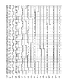
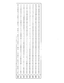
次に、上述のグレイコードカウンタにおいて、グレイコードの各ビットの作成について、図1の回路図、図2の動作タイミング図、図3のグレイコードを参照して具体的に説明する。なお、図2、図3は便宜上、グレイコードの途中までを示している。なお、グレイコードカウンタは、RDFF1〜9およびRDFF31〜38がそれぞれリセット信号RESETによりリセットされてから動作を開始する。
Next, with reference to the circuit diagram of FIG. 1, the operation timing chart of FIG. 2, and the gray code of FIG. 2 and 3 show the middle of the gray code for convenience. Note that the gray code counter starts operating after the
第1ビットのグレイコードQ0は、RDFF2の出力信号Q0Oを、RDFF31を通してクロックCLKに同期させて出力することで得られる。つまり、RDFF31はRDFF2の出力信号Q0OをクロックCLKの立ち上がりに同期してデータ入力端子Dから取り込んで保持し、次のクロックCLKの立ち上がりに同期して、出力端子Qから出力する。同様に、第2ビットのグレイコードQ1は、RDFF3の出力信号Q1Oを、RDFF32を通してクロックCLKに同期させて出力することで得られる。 Gray code Q0 of the first bit, the output signal Q0 O of RDFF2, obtained by outputting in synchronization with the clock CLK through RDFF31. That, RDFF31 holds captures the synchronization with the data input terminal D of the output signal Q0 O to the rise of the clock CLK RDFF2, in synchronization with the rising edge of the next clock CLK, and output from the output terminal Q. Similarly, Gray code Q1 of the second bit, the output signal Q1 O of RDFF3, obtained by outputting in synchronization with the clock CLK through RDFF32.
第3ビットのグレイコードQ2については、RDFF4の出力信号Q2Oを、選択回路21によって遅延させ、RDFF33を通してクロックCLKに同期させて出力することで得られる。即ち、選択回路21は第1ビットの反転グレイコードQN0が「1」の時に、出力信号Q2Oを選択して、これをRDFF33に入力する。
The Gray code Q2 of the third bit, the output signal Q2 O of RDFF4, delayed by the
第4ビットのグレイコードQ3については、RDFF5の出力信号Q3Oを、AND回路11及び選択回路22によって遅延させ、RDFF34を通してクロックCLKに同期させて出力することで得られる。即ち、第1ビットの反転グレイコードQN0及び第2ビットの反転グレイコードQN1が「1」の時にAND回路11の出力は「1」になるので、このとき選択回路22は、出力信号Q3Oを選択して、これをRDFF34に入力する。
The Gray code Q3 of the fourth bit, the output signal Q3 O of RDFF5, delayed by the
第5ビットのグレイコードQ4については、RDFF6の出力信号Q4Oを、AND回路12及び選択回路23によって遅延させ、RDFF35を通してクロックCLKに同期させて出力することで得られる。即ち、QN0、QN1、QN2が「1」の時にAND回路12の出力は「1」になるので、このとき選択回路23は、出力信号Q4Oを選択して、これをRDFF35に入力する。
The Gray code Q4 fifth bit, the output signal Q4 O of RDFF6, delayed by the
第6ビットのグレイコードQ5については、RDFF7の出力信号Q5Oを、AND回路13及び選択回路24によって遅延させ、RDFF36を通してクロックCLKに同期させて出力することで得られる。即ち、QN0、QN1、QN2、QN3が「1」の時にAND回路13の出力は「1」になるので、このとき選択回路24は、出力信号Q5Oを選択して、これをRDFF36に入力する。
The Gray code Q5 sixth bit, the output signal Q5 O of RDFF7, delayed by the
第7ビットのグレイコードQ6については、RDFF8の出力信号Q6Oを、AND回路14及び選択回路25によって遅延させ、RDFF37を通してクロックCLKに同期させて出力することで得られる。即ち、QN0、QN1、QN2、QN3、QN4が「1」の時にAND回路14の出力は「1」になるので、このとき選択回路25は、出力信号Q6Oを選択して、これをRDFF37に入力する。
The Gray code Q6 of the seventh bit, the output signal Q6 O of RDFF8, delayed by the
第8ビットのグレイコードQ7については、RDFF9の出力信号Q7Oを、AND回路15及び選択回路26によって遅延させ、RDFF38を通してクロックCLKに同期させて出力することで得られる。即ち、QN0、QN1、QN2、QN3、QN4、QN5が「1」の時にAND回路15の出力は「1」になるので、このとき選択回路26は、出力信号Q7Oを選択して、これをRDFF38に入力する。
The eighth bit of the Gray code Q7, the output signal Q7 O of RDFF9, delayed by the
なお、AND回路11〜26は、対応するグレイコードが入力されたNOR回路によって置き換えることができる。例えば、AND回路11は、第1ビットのグレイコードQ0と第2ビットのグレイコードQ1が入力されたNOR回路と等価である。
The
以上、8ビットのグレイコードカウンタについて説明したが、9ビット以上についても同様である。一般に第nビット(nは、4以上の自然数)のグレイコードは、第nビットに対応する分周回路の出力を、AND回路と選択回路によって遅延させ、RDFFを通してクロックCLKに同期させて出力することで得られる。この場合、AND回路は、反転グレイコードの第1ビットから第(n−2)ビットまでの(n−2)ビットが入力される。 Although the 8-bit gray code counter has been described above, the same applies to 9 bits or more. In general, the Gray code of the nth bit (n is a natural number of 4 or more) delays the output of the frequency dividing circuit corresponding to the nth bit by the AND circuit and the selection circuit, and outputs it in synchronization with the clock CLK through the RDFF. Can be obtained. In this case, the AND circuit receives (n-2) bits from the first bit to the (n-2) th bit of the inverted gray code.
そして、選択回路はAND回路の出力が「1」の時に、前記分周回路の出力を選択し、選択回路はAND回路の出力が「1」の時には、RDFFの出力を選択する。また、上述のようにAND回路は第1ビットから第(n−2)ビットまでの(n−2)ビット分のグレイコードが入力されたNOR回路で置き換えることができる。 The selection circuit selects the output of the frequency dividing circuit when the output of the AND circuit is “1”, and the selection circuit selects the output of the RDFF when the output of the AND circuit is “1”. Further, as described above, the AND circuit can be replaced with a NOR circuit to which gray codes for (n-2) bits from the first bit to the (n-2) th bit are input.
このように、本発明によれば、グレイコードの各ビットは下位ビットについては、分周回路とRDFFだけで構成され、上位ビットについては、分周回路、AND回路、選択回路、RDFFだけで構成されているので、回路構成が簡単であり、クリティカルパスの遅延時間が短縮化され、高速動作が可能なグレイコードカウンタを実現することができる。特に、上位ビットに対応する回路のクリティカルパスは、分周回路から出力のRDFFに至るパスであるが、AND回路の入力信号は下位ビットのグレイコードであるから、その時点ですでに確定しており遅延時間は非常に短い。また、選択回路は2つの信号のいずれかを選択するだけであるから遅延時間は非常に短い。 As described above, according to the present invention, each bit of the Gray code is composed of only the frequency divider and the RDFF for the lower bits, and only the frequency divider, the AND circuit, the selection circuit, and the RDFF for the upper bits. Therefore, the circuit configuration is simple, the delay time of the critical path is shortened, and a gray code counter capable of high-speed operation can be realized. In particular, the critical path of the circuit corresponding to the upper bit is a path from the frequency divider circuit to the output RDFF, but since the input signal of the AND circuit is the gray code of the lower bit, it has already been determined at that time. The delay time is very short. Further, since the selection circuit only selects one of the two signals, the delay time is very short.
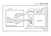
次に、本発明のグレイコードカウンタを用いた液晶表示装置について説明する。図4はそのような液晶表示装置のブロック図である。液晶表示装置101において、液晶表示パネル101P上に表示エリア(画素エリア)、水平ドライバ101H、垂直ドライバ101Vが形成され、表示パネル101Pの外部にタイミングコントローラIC102が設けられている。タイミングコントローラIC102内に、本発明のグレイコードカウンタ103と、このグレイコードカウンタ103が生成したグレイコードをデコードしてそれぞれ水平スタートパルスSTH、垂直スタートパルスSTVを作成するデコーダ104H、104Vが設けられている。タイミングコントローラIC102によって作成された水平スタートパルスSTH、垂直スタートパルスSTVはそれぞれ、水平ドライバ101H、垂直ドライバ101Vに入力される。そして、水平ドライバ101Hは水平スタートパルスSTHを順次転送して水平走査信号を作成し、垂直ドライバ101Vは垂直スタートパルスSTVを順次転送して垂直走査信号を作成する。
Next, a liquid crystal display device using the gray code counter of the present invention will be described. FIG. 4 is a block diagram of such a liquid crystal display device. In the liquid
したがって、この液晶表示装置101によれば、グレイコードカウンタ103の高速動作が可能なので、液晶表示装置101の全体の高速化が可能になる。グレイコードカウンタ103は、TFTで形成することができるので、低温ポリシリコン技術を用いて、液晶表示パネル101Pを構成しているガラス基板上に水平ドライバ101H、垂直ドライバ101V等と共に形成してもよい。これにより、半導体部品点数の削減、組立の簡便化が図れるので、外部回路基板のサイズも小さくでき、液晶表示装置101全体として小型化及び軽量化を図ることができる。また、本発明のグレイコードカウンタは、液晶表示装置だけでなく、有機EL表示装置などの他の表示装置にも同様に用いることができる。
Therefore, according to the liquid
1〜9 D型フリップフロップ(RDFF)
11〜15 AND回路
21〜26 選択回路
31〜38 D型フリップフロップ(RDFF)
101 液晶表示装置 101P 表示パネル
101H 水平ドライバ 101V 垂直ドライバ
102 タイミングコントローラIC
103 グレイコードカウンタ
104H,104V デコーダ
1-9 D-type flip-flop (RDFF)
11-15 AND circuits 21-26 selection circuits 31-38 D-type flip-flop (RDFF)
101 Liquid
103
Claims (4)
第nビットのグレイコードの1つ下位ビットである第(n−1)ビットのグレイコードのクロックを2分周する分周回路と、
前記分周回路の出力を第(n−2)ビット以下のグレイコードに基づいて遅延する遅延回路と、
前記遅延回路の出力をクロックに応じて保持し、かつ遅延して、第nビットのグレイコードを出力する順序回路と、を備えることを特徴とするグレイコードカウンタ。 In the Gray code counter that generates the Gray code,
A frequency dividing circuit that divides the clock of the (n-1) th bit Gray code, which is one lower bit of the nth bit Gray code, by two;
A delay circuit that delays the output of the frequency divider circuit based on a Gray code of (n-2) th bit or less;
A gray code counter comprising: a sequential circuit that holds an output of the delay circuit in accordance with a clock, and outputs a delayed n-bit gray code.
Priority Applications (2)
| Application Number | Priority Date | Filing Date | Title |
|---|---|---|---|
| JP2007075958A JP4292425B2 (en) | 2007-03-15 | 2007-03-23 | Gray code counter and display device |
| US12/036,031 US7596201B2 (en) | 2007-03-15 | 2008-02-22 | Gray code counter and display device therewith |
Applications Claiming Priority (2)
| Application Number | Priority Date | Filing Date | Title |
|---|---|---|---|
| JP2007066104 | 2007-03-15 | ||
| JP2007075958A JP4292425B2 (en) | 2007-03-15 | 2007-03-23 | Gray code counter and display device |
Publications (2)
| Publication Number | Publication Date |
|---|---|
| JP2008258660A JP2008258660A (en) | 2008-10-23 |
| JP4292425B2 true JP4292425B2 (en) | 2009-07-08 |
Family
ID=39981837
Family Applications (1)
| Application Number | Title | Priority Date | Filing Date |
|---|---|---|---|
| JP2007075958A Active JP4292425B2 (en) | 2007-03-15 | 2007-03-23 | Gray code counter and display device |
Country Status (1)
| Country | Link |
|---|---|
| JP (1) | JP4292425B2 (en) |
Families Citing this family (3)
| Publication number | Priority date | Publication date | Assignee | Title |
|---|---|---|---|---|
| KR102664062B1 (en) * | 2019-05-30 | 2024-05-14 | 삼성전자주식회사 | Code generator comprising asynchronous counter and synchronous counter, and operating method thereof |
| KR102868858B1 (en) * | 2019-11-27 | 2025-10-10 | 삼성전자주식회사 | Gray counter and image sensor comprising the same |
| JP7570899B2 (en) * | 2020-11-25 | 2024-10-22 | シャープセミコンダクターイノベーション株式会社 | Multi-bit Gray code generator |
-
2007
- 2007-03-23 JP JP2007075958A patent/JP4292425B2/en active Active
Also Published As
| Publication number | Publication date |
|---|---|
| JP2008258660A (en) | 2008-10-23 |
Similar Documents
| Publication | Publication Date | Title |
|---|---|---|
| US7596201B2 (en) | Gray code counter and display device therewith | |
| CN100583295C (en) | Shift register and LCD device | |
| CN102968952B (en) | Scan driver and organic light emitting display device using thereof | |
| JP4093197B2 (en) | Display driver and electronic device | |
| CN102298916B (en) | Driving circuit, liquid crystal display apparatus and electronic information device | |
| CN106960655B (en) | A gate drive circuit and display panel | |
| JP6115407B2 (en) | Display panel, driving method thereof, and electronic apparatus | |
| JP4292425B2 (en) | Gray code counter and display device | |
| CN112908275B (en) | Data signal line driver circuit and liquid crystal display device having the same | |
| JP2009246482A (en) | Priority encoder and time digital converter using it, and test device | |
| US20070146290A1 (en) | Device for driving a display panel | |
| JP6650459B2 (en) | Display panel and its driving circuit | |
| JP2014179777A (en) | Output circuit, selection circuit, gate driver circuit, display device and matrix device | |
| JP6775640B2 (en) | Gray code counter | |
| CN101079244B (en) | display image system | |
| JP2007006368A (en) | A/d conversion circuit | |
| JP2015005874A (en) | Semiconductor device, display device and signal capture method | |
| JP4762251B2 (en) | Liquid crystal display device and driving method thereof | |
| US20090040213A1 (en) | Liquid Crystal Driving Apparatus | |
| GB2403082A (en) | Arrangement and method for a digital delay line | |
| JP4666462B2 (en) | Counter circuit and semiconductor device including the same | |
| CN102024401B (en) | Driving device, display panel, display device and electronic system | |
| KR101152461B1 (en) | Asynchronous gray-code counter | |
| JP2008131071A (en) | Gray code counter and display device | |
| JP4581667B2 (en) | Timing generator and display device |
Legal Events
| Date | Code | Title | Description |
|---|---|---|---|
| A131 | Notification of reasons for refusal |
Free format text: JAPANESE INTERMEDIATE CODE: A131 Effective date: 20090106 |
|
| A521 | Written amendment |
Free format text: JAPANESE INTERMEDIATE CODE: A523 Effective date: 20090217 |
|
| TRDD | Decision of grant or rejection written | ||
| A01 | Written decision to grant a patent or to grant a registration (utility model) |
Free format text: JAPANESE INTERMEDIATE CODE: A01 Effective date: 20090311 |
|
| A01 | Written decision to grant a patent or to grant a registration (utility model) |
Free format text: JAPANESE INTERMEDIATE CODE: A01 |
|
| A61 | First payment of annual fees (during grant procedure) |
Free format text: JAPANESE INTERMEDIATE CODE: A61 Effective date: 20090324 |
|
| FPAY | Renewal fee payment (event date is renewal date of database) |
Free format text: PAYMENT UNTIL: 20120417 Year of fee payment: 3 |
|
| R150 | Certificate of patent or registration of utility model |
Ref document number: 4292425 Country of ref document: JP Free format text: JAPANESE INTERMEDIATE CODE: R150 Free format text: JAPANESE INTERMEDIATE CODE: R150 |
|
| FPAY | Renewal fee payment (event date is renewal date of database) |
Free format text: PAYMENT UNTIL: 20120417 Year of fee payment: 3 |
|
| FPAY | Renewal fee payment (event date is renewal date of database) |
Free format text: PAYMENT UNTIL: 20130417 Year of fee payment: 4 |
|
| FPAY | Renewal fee payment (event date is renewal date of database) |
Free format text: PAYMENT UNTIL: 20130417 Year of fee payment: 4 |
|
| FPAY | Renewal fee payment (event date is renewal date of database) |
Free format text: PAYMENT UNTIL: 20140417 Year of fee payment: 5 |
|
| R250 | Receipt of annual fees |
Free format text: JAPANESE INTERMEDIATE CODE: R250 |
|
| R250 | Receipt of annual fees |
Free format text: JAPANESE INTERMEDIATE CODE: R250 |