JP4292002B2 - Plasma processing equipment - Google Patents
Plasma processing equipment Download PDFInfo
- Publication number
- JP4292002B2 JP4292002B2 JP2002366163A JP2002366163A JP4292002B2 JP 4292002 B2 JP4292002 B2 JP 4292002B2 JP 2002366163 A JP2002366163 A JP 2002366163A JP 2002366163 A JP2002366163 A JP 2002366163A JP 4292002 B2 JP4292002 B2 JP 4292002B2
- Authority
- JP
- Japan
- Prior art keywords
- gas
- electrode
- flat plate
- gas supply
- protrusion
- Prior art date
- Legal status (The legal status is an assumption and is not a legal conclusion. Google has not performed a legal analysis and makes no representation as to the accuracy of the status listed.)
- Expired - Lifetime
Links
Images


Landscapes
- Plasma Technology (AREA)
- Physical Or Chemical Processes And Apparatus (AREA)
- Chemical Vapour Deposition (AREA)
Description
【0001】
【発明の属する技術分野】
本発明は、半導体製造工程に用いるプラズマ処理装置に関するものである。
【0002】
【従来の技術】
プラズマ処理装置は、エッチングや薄膜堆積など、プラズマ固有の性質を生かした加工技術の実現により、今や産業界に不可欠な半導体基盤技術としてその重要度が増している。
中でも種々の基板上に電子材料の層を堆積するプラズマ促進化学気相堆積法(Plasma Enhanced Chemical Vapor Deposition:PECVD)を用いたプラズマ処理装置は、半導体デバイスの製造に広く用いられている。
【0003】
PECVDを用いたプラズマ処理装置としては、ホローカソード現象を利用して高密度プラズマを得るとともに、メンテナンスサイクルを延ばし、電極のフッ化減少を改善したものが知られている(例えば、特許文献1参照。)。
【0004】
特許文献1のプラズマ処理装置は、図16に示すように、平行平板電極構造をしており、気密な処理室1に基板4を収容し、処理室1内に設けられている一対の平板電極2、3間に成膜ガスを供給しながら高周波電力を印加してプラズマを発生させ、成膜ガス中のガス分子を分解して化学反応を起こし、基板表面上に薄膜を形成するものである。
成膜ガスは、カソード電極2に接続されたガス導入口15を通って供給され、カソード電極2に設けた分散板12、ガス導入孔5を経由してカソード電極2とアノード電極3間へと導入される。アノード電極3と対向するカソード電極2の平板部45に、電極面積を拡大するための凹部70を複数設けてある。この凹部70にはガス供給口は設けずに、凹部70を設けずに残ったアノード電極3の平板部分にガス供給孔5を設けてある。ガス導入口15から先に非成膜ガスを導入し、後から成膜ガスを導入する。これにより非成膜ガスを凹部に入り込ませ、後から導入される成膜ガスが凹部70に入らないようにしている。
電極2、3間へ導入された成膜ガスに、結合コンデンサ19、ガス導入口15、アノードサセプタ13を経由したRF高周波電源9の高周波電力を電極3に印加してプラズマを発生させ、基板4上に所定の成膜を行う。なお、上ヒータ10と下ヒータ11は、基板4を一定の温度に均一に加熱するために設けられている。
【0005】
このように特許文献1のプラズマ処理装置によれば、電極に複数の凹部を設けたので、非成膜ガスが凹部70内に滞留することになって、凹部70内に成膜ガスによる累積形成膜が形成されにくくなり、メンテナンスサイクルの長期化を可能としている。また、非成膜ガスが滞留した凹部70からホローカソード現象により高密度エネルギーが出て、凹部70以外の平板部分に設けたガス供給孔5から導入される成膜ガスを有効に電離するので、凹部70を形成していないものに比べて、必要とする高周波電力を低減でき、電極2、3間に加わる直流電圧が大幅に小さくなり、電極シース電位勾配を緩やかにすることができる。その結果、高周波電力を印加する側の電極2でのスパッタリング現象等が抑制され、電極2へのフッ化物の生成を低減している。
【0006】
【特許文献1】
特開2001−135626号公報
【0007】
【発明が解決しようとする課題】
上述した特許文献1によれば、一対の平板電極のうち高周波電力を印加する側の平板電極に複数の凹部を設けて電極面積を増加したので、凹部を設けないものに比べて、フッ化物の生成の低減とともに、低い高周波電力で成膜ガスを有効に電離できるので、プラズマ生成効率は改善されている。しかしながら、この場合でも、ガス供給孔が電極の平板部分に設けられているので、高周波電力によって形成される電極間の電界を、この平板部分に設けられているガス供給孔から導入されるガス分子に、より有効に作用するようには企図されていないため、プラズマ生成効率に改善の余地がある。
【0008】
そこで本発明の目的は、ガス供給孔から導入されるガス分子に、より有効に電界を作用するようして、プラズマ生成効率を向上させることを可能としたプラズマ処理装置を提供することにある。
【0009】
【課題を解決するための手段】
前記目的を達成するために、対向する一対の平板電極間にガスを供給し、一対の平板電極の少なくとも一方の平板電極に高周波電力を印加してプラズマを発生させて基板にプラズマ処理を行うプラズマ処理装置において、前記高周波電力が印加される平板電極に複数の突起を設け、前記複数の突起に前記ガスを供給するガス供給孔を設けたことを特徴とするプラズマ処理装置である。
【0010】
このように構成することにより、突起を設けた平板電極の周囲に存在する電子が加速され、突起に設けられたガス供給孔を通って平板電極間に供給されたガスの分子と衝突する。このガス分子は衝突によって正イオンと電子に分れ、分子に衝突した電子、及び分子から電離した電子は、さらに別のガス分子と衝突する。これが連鎖的に繰り返されることによってガス分子の電離が促進され、プラズマが生成する。平板電極に設けた突起には電界の勾配が形成され、突起先端に向かって電界が高くなるので、その周辺の電子は加速されやすく、連鎖的な衝突及びガス分子の電離が激しく繰り返されて電子密度が高くなり、プラズマ生成効率が向上する。
【0011】
また、突起を設けた平板電極では、平板電極間に突出した突起先端で最もホロー放電が生じやすく、突起先端で生じたホロー放電による効果は突起側面を伝わり電極表面に達する。電極表面は突起によって分断されることなく全体がひとつながりであるため、突起先端から生じたホロー放電による効果は電極全体に広がる。
【0012】
前記突起が設けられた平板電極の突起間の平板部にも、前記ガス供給孔を設けることが好ましい。これにより、平板電極の突起間の平板部に設けたガス供給口から突起間にガスが供給されると、平板電極の突起間に生じるホローカソード現象が促進し、より電子密度を高くすることができる。また、平板電極の突起間の平板部にガスが流れると、突起間の平板部に滞留するパーティクルが、このガスにより突起間から押し出されるので、滞留したパーティクルを有効に除去できる。
【0013】
【発明の実施の形態】
以下、本発明の実施の形態を添付図面に基づいて詳述する。
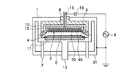
まず、図1を用いて、PECVDを用いて成膜処理を行うプラズマ処理装置の全体構成を説明する。
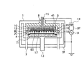
図1に示すように、プラズマ処理装置の処理室1は、インナケース18とアウタケース31とからなる減圧可能な二槽構造となっている。密閉されたアウタケース31の内部にインナケース18が設けられる。インナケース18はアウタケース31の天井に取り付けられて上部が閉じ底部が開口したケース本体と、底部開口を塞ぐケース外蓋としてのアノードサセプタ13とから構成される。
【0014】
処理室1内には一対の平行平板電極が設けられる。一方はアノード電極3、他方はカソード電極17を構成する。一方のアノード電極3は、アノードサセプタ13上に支持される。アノード電極3上に基板4が載置され、基板4の外周には絶縁リング16が設けられる。アノード電極3は、アノード電極3を支持するアノードサセプタ13を通して接地される。
【0015】
他方のカソード電極17は、上部全面をインナケース18のケース本体内に設けられた絶縁ケース8で覆われる。カソード電極17の下部外周は絶縁リング20により支持されることで、接地されている処理室1のインナケース18及びアウタケース31とは絶縁されている。
【0016】
カソード電極17は、ガス供給ヘッド35の一部を構成する。すなわち、ガスガス供給ヘッド35は、絶縁ケース8から引き出されて成膜ガスを処理室1内に導入するガス導入口15と、ガス導入口15から導入されたガスを分散する分散板12と、高周波電力を印加されるカソード電極17とから構成される。このカソード電極17は、ガス導入口15から分散板12を介して導入される成膜ガスを一対の電極3、17間に供給する複数のガス供給孔40を有する。
【0017】
RF高周波電源9はマッチングボックス37及び結合コンデンサ19を介してガス導入口15からカソード電極17に接続される。アノード電極3を支持するアノードサセプタ13の接地は、インナケース18及びアウタケース31を介してなされる。
【0018】
成膜ガスは、ガス導入口15を通って処理室1内へ供給され、カソード電極17に設けた分散板12、ガス供給孔40を経由して電極3、17間へと導かれる。カソード電極17に設けられた上ヒータ10と、アノード電極3に設けられた下ヒータ11は、基板4を一定の温度に均一に加熱するために設けられている。
【0019】
基板4を載置するアノードサセプタ13は昇降移動するようになっている。アノードサセプタ13は、上昇時、インナケース18の下部開口を閉じて内槽を形成し、その内槽内に基板4を閉じ込める。下降時、内槽を開いて、基板4を外槽となるアウタケース31へ取り出す。
【0020】
成膜時は、アノードサセプタ13を上昇して内槽を形成する。カソード電極17とアノード電極3間に導入された成膜ガスに、RF高周波電源9の高周波電力を印加してプラズマを発生させ、基板4上に所定の成膜を行う。プラズマにより処理された成膜ガスの残留ガスは、処理室1に連通する排気管7を通り、図示しない排気処理系へと処理される。なお、図中、ガス供給系、基板搬送系、排気処理系は省略してある。
【0021】
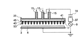
図2〜図4は、上述したプラズマ処理装置の構成を機能ごとに捉らえてユニット化して示した説明図である。図2はプラズマ処理装置の基本構成図である。図3は一対の平板電極を構成する高周波プラズマ生成電極の構成図である。図4は高周波プラズマ生成電極を構成するカソード電極を含むガス供給ヘッドの構成図である。
これらの図では、ガス供給ヘッド35は、ガス導入口15と、ガス導入口に連通した中空のヘッド本体と、ヘッド本体の底部を構成するカソード電極17とから主に構成される。ガス導入口15は3本設けられ、3本のうちの1本には成膜ガスを流し、残りの2本にはプラズマ生成用ガス、例えばアルゴン(Ar)ガスを流すように構成される。成膜ガスを流す1本のガス導入口15には、RF高周波電源9をマッチングボックス37及び結合コンデンサ19を介して接続し高周波電力を印加する。アノード電極3は接地する。
また、カソード電極17は、アノード電極3と対向する平板部45と、その平板部45に電界勾配を形成するための複数の突起50と、各突起50に設けられた第1の供給孔となるガス供給孔40とから構成される。平板部45と突起50とは個別に形成しても一体に形成してもよい。この場合、突起50の一部を平板部45に設けた孔に圧入することにより一体化してもよい。
【0022】
また、カソード電極17の突起50の間の平板部45には、第2の供給孔となるガス供給孔41を設けることが好ましい。この平板部45のガス供給孔41の径は、突起50のガス供給孔41の径との関係で決められる。例えば、第1のガス供給孔41の直径を0.8mmとすれば、その倍の直径1.6mmがよい。
このガス供給孔41は、例えば、カソード電極17の平板部45に多数の貫通孔を設け、これら貫通孔の一部に突起50を設けて、残りの貫通孔をガス供給孔41として利用するようにしてもよい。
なお、ガス導入口15とアノード電極3とをつなぐ中空のヘッド本体は、内部の分散板12の記載を省略してある。
【0023】
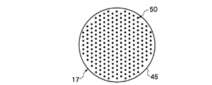
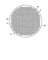
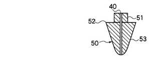
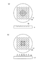
カソード電極17の平板部45に設ける複数の突起50は、平板部45のほぼ全面に配置するが、例えば、図5〜図7に示すように配置するとよい。図5では碁盤の目状に配置して隣り合う4つの突起を直線で結ぶと四角形状になるようにしている。図6は碁盤の目をずらして隣り合う4つの突起を直線で結ぶと菱形となるようにしている。図7ではさらにずらしてランダム状に配置している。
突起50の形状は、電界勾配を付けることができるように形成し、例えばアノード電極3に向って突出する形状に形成される。具体的には、図9〜図12に例示するような形状とするとよい。図9には先端部が半球形をした円柱状のもの、図10は先端部が円錐形をした円柱状のもの、図11は円錐状のもの、図12は断面半楕円状のものがそれぞれ示されている。なおこの他に、先端部が三角錐状、四角錐状、多角錐状をしていてもよい。
これらに示された突起50は、カソード電極17の平板部45(例えば貫通孔)に装着される円柱状の装着部51と、その装着部51に同軸に一体的に設けられ、装着部51との境目(基端部)52が装着部51及び平板部45の貫通孔より径が大きく形成されて平板部45から突出する突出部53とから形成されている。この突起50の軸にその軸方向に沿ってガス供給孔40が設けられている。
【0024】
装着部51の直径は、平板部45の貫通孔の径と同じか若干小さな径に形成される。また、突起50が圧入により装着される場合には、装着部51の直径は、平板部45の貫通孔の径より若干大きな径に形成される。また、装着部51の軸方向の長さは、平板部45の厚さにもよるが、好ましくは平板部45の厚さと同じにすることがよい。
【0025】
突起50の平板部45への装着は、例えば、平板部45に貫通孔を設け、この貫通孔に突起50の装着部51を圧入して行ってもよいし、平板部45の貫通孔に突起50の装着部51を挿入した後、溶接等により固着して行ってもよい。また、装着部51の外周にねじ山を設け、このねじ山に螺合するねじ溝を平板部45の貫通孔を形成する壁に設けて、ねじ止めによって行うようにしてもよい。
【0026】
このように、カソード電極17のアノード電極3と対向する側の面に、突起先端にいくほど電界強度が高くなる電界勾配を形成するための突起50を複数配置し、この突起50内に設けたガス供給孔40を通過するガス分子が、電界勾配によって加速されるようにする。
【0027】
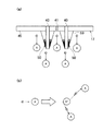
このことを、図14を用いて説明する。この図14は、カソード電極17に高周波電力が印加されていると共に、突起50内に設けた第1の供給孔であるガス供給孔40から成膜ガスが供給されている状態を示すものである。
まず、カソード電極17に高周波電力が印加されると、アノード電極3に向って突出する突起50は、先端にいくにつれて電界が高くなる。図14では、電界が高くなる様子を分かり易いようにドットの濃淡で表示した。このように電界が突起50の先端にいくにつれて高くなると、突起50の周囲に存在する電子e-は加速されることになる。
【0028】
カソード電極17の平板部45に設けた突起50の周囲に存在する電子e-が加速されると、この加速された電子e-は、突起50に設けられたガス供給孔40を通って電極3、17間の空間に供給された成膜ガスの分子Aと衝突する(図14(a))。このガス分子Aは衝突によってA+イオンと電子e-に分れ、ガス分子Aに衝突した電子e-及びガス分子Aから電離した電子e-は、軽量であるためさらに別のガス分子と衝突する(図14(b))。これが連鎖的に繰り返されることによってガス分子の電離が促進され、プラズマが生成する。平板部45に設けた突起50には電界の勾配が形成され、突起先端で電界が高くなるので、その周辺の電子e-は特に高速に加速されやすく、連鎖的な衝突及びガス分子Aの電離が激しく繰り返されて電子密度が特に高くなり、プラズマ生成効率が向上する。
【0029】
なお、衝突により分かれたA+イオンが衝突の勢いで別の分子に衝突することもあるが、A+イオンより電子e-のほうがはるかに軽量であるので、圧倒的に電子による衝突が多いと考えられる。
また、衝突の激しさは、ガスの圧力や高周波電源の出力などによって変わるが、基本的な衝突の原理は図14を用いて説明したものと同じであると考えられる。
【0030】
なお、従来例で説明した図16のカソード電極2も、平板部に凹部を設けることで、カソード電極2に相対的に凸部が形成されることになる。しかし、この従来例の凸部と実施の形態の突起50とは基本的に構成が異なる。従来例のものでは、平板部に設けた凹部70は互いに独立して存在しているが、この凹部70を設けることなく取り残された平板部分は、凹部70からみて相対的に凸部になっているとしても、この凸部は独立して存在しているわけではなく、面一のものとして互いにつながっている。これに対して実施の形態の突起50は、平板部45から突出させているので、独立した存在であり、つながっていない。また、従来例のものでは、相対的に凸部となっている平板部分にガス供給孔5を設けているため、このガス供給孔5に沿って電界の勾配が生じない。これに対して、実施の形態のものでは平板部45から突出した突起にガス供給孔50を設けているので、電界勾配が生じ、先端にいくにしたがって電界集中を起こすことができる。
したがって、従来例のものでは、ガス分子はこれを加速するように電界の影響をガス供給孔50内で受けないので、ガス供給孔5から出るガスの分子が凸部によっては加速されることはなく、したがって電子密度は高めることができない。
【0031】
したがって、実施の形態のように、電界勾配を形成するための突起50を設け、この突起50からガスを供給することにより、ガスの分子及び電子による衝突が増えるので、電子密度が高くなり、その結果、プラズマ生成効率を向上でき、必要とする高周波電力をより低減できる。
【0032】
また、突起50を設けると、ホローカソード現象によるプラズマ密度を増加できる。ホローカソード現象を生かした電極構造として、既に図17の(a)のような平板電極2の電極表面に多数の凹部(くぼみ)70を設けたものが知られている。しかし、ホロー放電は空間に突出した部分ほど生じやすいので、この凹部構造では凹部70の周縁部で最もホロー放電が起こりやすく、しかも周縁部は分断されることなく全体がひとつながりであるため、放電による効果は矢印で示すように周縁部全体に広がってしまい、凹部70の内側には伝播しにくい(ホローカソード現象によるプラズマ密度の増加は、凹部が1つだけの場合が最も効果的である)。一方、実施の形態による平板電極17では、空間に突出した突起50の先端で最もホロー放電が生じやすく、図17(b)に示すように、突起先端で生じたホロー放電による効果は突起50側面を伝わり平板電極17の電極表面に達する。電極表面は突起50によって分断されることなく、全体がひとつながりであるため、突起先端から生じた放電による効果は矢印で示すように平板電極全体に広がる。
【0033】
また、カソード電極17の突起50の間の平板部45にガス供給孔41を設けると、このガス供給孔41から供給されたガスによって突起50の間にガスの分子が滞留することなく、突起50の間以外の平板電極3、17間に押し出される。これにより、突起50の間にガスの分子が滞留する場合に比して突起50の間以外の平板電極3、17間にガスの分子が多く存在するので、前記の衝突が起こりやすくなり、より電子密度を高くすることができる。また、カソード電極17の突起50の間の平板部45にガス供給孔41を設けて、このガス供給孔41から突起50間に直接ガスを流すことにより、エネルギーの拡散を強めてホローカソード現象を促進することができ、より一層電子密度を高くすることができる。
【0034】
また、カソード電極17の突起50の間の平板部45にガス供給孔41を設けると、突起50の間の平板部45の表面上にパーティクルがたまりやすいが、ガス供給孔41からのガスの供給により、そのパーティクルを除去することができるので、パーティクルの集積も防ぐことが可能となる。
【0035】
【実施例】
凹凸電極であって凹凸部両方に孔を設けた突起付のカソード電極17を用いて電子密度の圧力依存性を調べた。
図1に示す構成のプラズマ処理装置を用い、処理室1内圧力を100〜1000mTorrに維持して、カソード電極17のガス供給孔40、41からアルゴンを流しつつ(凹凸部両方の孔からガス供給し)、20mm離間して配設された一対の直径165mmの電極17、3間に周波数13.56MHz、出力20Wの高周波電力を印加し、一対の電極17、3間の電子密度を調べた。電子密度は、Mo製シングルプローブをプラズマの中心位置に挿入して測定し、その結果を図15に示した。
上記突起付カソード電極としては図8に示すものを用いた。このカソード電極17は碁盤目状に配置され、その突起50の個数は373個である。平板部45のガス供給孔41は、突起50を避けるように、碁盤目状に配置され、その個数は352個であり、その直径は1.6mmである。
突起50としては図13に示す形状の、ガス供給孔直径:0.8、突起傾斜広がり角度:40°、装着部直径:2.2mm、長さ:2.5mm、突出部長さ:6.3mm、基端部直径:6mmのものを用いた。突起50のカソード電極への取付けは、装着部51の外周にねじ山56を設け、このねじ山56に螺合するねじ溝を平板部45の貫通孔を形成する壁に設けて、ねじ止めによって行った。
また、比較のために上記突起付カソード電極と同一の電極を用いるが、どちらのガス供給孔からもガスを供給せずに、代りに一対の電極間にアルゴンを供給する場合(凹凸部どちらの孔からもガス供給なし)と、カソード電極として平板円盤状の平行平板電極を用いた場合(平行平板電極)とについても前記と同様にして電子密度を調べた。
【0036】
図15に示した結果から、実施の形態の突起付カソード電極17を用いた(凹凸部両方の孔からガス供給)場合は、圧力100、200、400、600、800、1000mTorrのいずれにおいても、凹凸のない平行平板電極の場合の2〜4倍ぐらいの電子密度の値となった。また、突起付カソード電極を用いても凹凸部どちらの孔からもガス供給なしの場合は、平行平板電極の場合の1.5〜2倍ぐらいの電子密度の値となった。
【0037】
したがって、実施の形態の突起付カソード電極17を用いて両方の孔からガスを供給することにより、電子密度を大きくすることができ、プラズマ生成効率を向上させることができる。
また、例えば、平行平板電極の場合の1.5倍の電子密度を得たいのであれば、実施の形態のカソード電極17のガス供給孔40,41の半分を閉塞させるとか、またはガスの流量と排気速度を下げるとかすることにより簡単に対応できることになる。
【0038】
【発明の効果】
本発明によれば、突起のガス供給孔を通るガスの分子は電界により加速されるため、他のガス分子と衝突して、この衝突のエネルギーによって分子はイオンと電子に分かれ、さらに軽量の電子等は別の分子と衝突し、このような衝突が連鎖的に繰り返されるので、電子密度を大きくすることができ、プラズマ生成効率を向上することができる。
【図面の簡単な説明】
【図1】実施形態によるプラズマ処理装置の全体構成図である。
【図2】実施形態によるプラズマ処理装置の基本構成図である。
【図3】実施形態による高周波プラズマ生成電極の構成図である。
【図4】実施形態によるカソード電極を含むガス供給ヘッドの構成図である。
【図5】実施形態によるカソード電極の平板部を示す平面図である。
【図6】実施形態によるカソード電極の平板部を示す平面図である。
【図7】実施形態によるカソード電極の平板部を示す平面図である。
【図8】具体的なカソード電極の平板部を示す平面図である。
【図9】実施形態による突起の断面図である。
【図10】実施形態による突起の断面図である。
【図11】実施形態による突起の断面図である。
【図12】実施形態による突起の断面図である。
【図13】具的的な突起の断面図である。
【図14】実施形態による突起のガス供給孔からの分子による衝突を説明する概念図である。
【図15】実施の形態のカソード電極を含む3種類のカソード電極を用いたプラズマ処理装置における電子密度の圧力依存性を示す比較図である。
【図16】従来例によるプラズマ処理装置の全体構成図である。
【図17】従来例と実施の形態とのホロー放電効果を比較した説明図であり、(a)は従来例、(b)は実施の形態である。
【符号の説明】
1 処理室
3 アノード電極
4 基板
7 排気管
9 RF高周波電源
15 ガス導入口
17 カソード電極
40 ガス供給孔
41 ガス供給孔[0001]
BACKGROUND OF THE INVENTION
The present invention relates to a plasma processing apparatus used in a semiconductor manufacturing process.
[0002]
[Prior art]
The importance of plasma processing apparatuses is now increasing as a semiconductor fundamental technology indispensable to the industry by realizing processing technologies that take advantage of plasma-specific properties such as etching and thin film deposition.
Among them, a plasma processing apparatus using plasma enhanced chemical vapor deposition (PECVD) for depositing a layer of an electronic material on various substrates is widely used for manufacturing semiconductor devices.
[0003]
As a plasma processing apparatus using PECVD, a high-density plasma is obtained by utilizing a hollow cathode phenomenon, and a maintenance cycle is extended to improve reduction in electrode fluorination (see, for example, Patent Document 1). .)
[0004]
As shown in FIG. 16, the plasma processing apparatus of Patent Document 1 has a parallel plate electrode structure, a
The film forming gas is supplied through a
Plasma is generated by applying high-frequency power of the RF high-
[0005]
As described above, according to the plasma processing apparatus of Patent Document 1, since the electrode is provided with the plurality of recesses, the non-film-forming gas stays in the
[0006]
[Patent Document 1]
Japanese Patent Laid-Open No. 2001-135626
[Problems to be solved by the invention]
According to Patent Document 1 described above, since the electrode area is increased by providing a plurality of recesses in the plate electrode on the side to which the high frequency power is applied among the pair of plate electrodes, compared to the electrode not having the recesses, As the generation is reduced, the film forming gas can be effectively ionized with a low high-frequency power, so that the plasma generation efficiency is improved. However, even in this case, since the gas supply hole is provided in the flat plate portion of the electrode, the electric field between the electrodes formed by the high frequency power is applied to the gas molecule introduced from the gas supply hole provided in the flat plate portion. However, since it is not intended to act more effectively, there is room for improvement in plasma generation efficiency.
[0008]
Accordingly, an object of the present invention is to provide a plasma processing apparatus capable of improving plasma generation efficiency by more effectively applying an electric field to gas molecules introduced from a gas supply hole.
[0009]
[Means for Solving the Problems]
In order to achieve the above object, a plasma is supplied to a substrate by supplying a gas between a pair of opposed flat plate electrodes, applying high frequency power to at least one flat plate electrode of the pair of flat plate electrodes to generate plasma. In the processing apparatus, the plate electrode to which the high-frequency power is applied is provided with a plurality of protrusions, and the gas supply holes for supplying the gas are provided in the plurality of protrusions.
[0010]
With this configuration, electrons existing around the plate electrode provided with the projection are accelerated and collide with gas molecules supplied between the plate electrodes through the gas supply hole provided in the projection. The gas molecules are separated into positive ions and electrons by collision, and the electrons colliding with the molecules and the electrons ionized from the molecules collide with another gas molecule. By repeating this in a chain, ionization of gas molecules is promoted and plasma is generated. An electric field gradient is formed on the projection provided on the plate electrode, and the electric field increases toward the tip of the projection, so that the electrons in the vicinity are easily accelerated, and the chain collision and ionization of gas molecules are repeated intensely. The density is increased and the plasma generation efficiency is improved.
[0011]
Further, in the flat electrode provided with the protrusion, the hollow discharge is most likely to occur at the tip of the protrusion protruding between the flat electrodes, and the effect of the hollow discharge generated at the tip of the protrusion is transmitted through the side surface of the protrusion and reaches the electrode surface. Since the entire surface of the electrode is connected without being divided by the protrusion, the effect of hollow discharge generated from the tip of the protrusion spreads over the entire electrode.
[0012]
Preferably, the gas supply hole is also provided in a flat plate portion between the protrusions of the flat plate electrode provided with the protrusion. As a result, when gas is supplied between the projections from the gas supply port provided in the flat plate portion between the projections of the flat plate electrode, the hollow cathode phenomenon generated between the projections of the flat plate electrode is promoted, and the electron density can be further increased. it can. Further, when the gas flows through the flat plate portion between the projections of the flat plate electrode, particles staying in the flat plate portion between the protrusions are pushed out from between the protrusions by this gas, so that the staying particles can be effectively removed.
[0013]
DETAILED DESCRIPTION OF THE INVENTION
Hereinafter, embodiments of the present invention will be described in detail with reference to the accompanying drawings.
First, the overall configuration of a plasma processing apparatus that performs film formation using PECVD will be described with reference to FIG.
As shown in FIG. 1, the processing chamber 1 of the plasma processing apparatus has a two-tank structure including an
[0014]
A pair of parallel plate electrodes are provided in the processing chamber 1. One constitutes the
[0015]
The
[0016]
The
[0017]
The RF high
[0018]
The film forming gas is supplied into the processing chamber 1 through the
[0019]
The
[0020]
During film formation, the
[0021]
2 to 4 are explanatory views showing the configuration of the plasma processing apparatus described above as a unit by grasping each function. FIG. 2 is a basic configuration diagram of the plasma processing apparatus. FIG. 3 is a configuration diagram of a high-frequency plasma generation electrode constituting a pair of flat plate electrodes. FIG. 4 is a configuration diagram of a gas supply head including a cathode electrode that constitutes a high-frequency plasma generation electrode.
In these drawings, the
Further, the
[0022]
Further, it is preferable to provide a
For example, the
Note that the description of the
[0023]
The plurality of
The shape of the
The
[0024]
The diameter of the mounting
[0025]
The mounting of the
[0026]
As described above, a plurality of
[0027]
This will be described with reference to FIG. FIG. 14 shows a state in which high-frequency power is applied to the
First, when high-frequency power is applied to the
[0028]
When the electrons e − existing around the
[0029]
Although sometimes the A + ions divided by the collision to collide with another molecule in momentum of the collision, electrons from A + ions e - since more of are much lighter, when many collisions overwhelmingly electronic Conceivable.
The severity of the collision varies depending on the gas pressure and the output of the high frequency power source, but the basic principle of the collision is considered to be the same as that described with reference to FIG.
[0030]
Note that the
Therefore, in the conventional example, since the gas molecules are not affected by the electric field in the
[0031]
Therefore, as in the embodiment, by providing the
[0032]
Further, when the
[0033]
Further, when the gas supply holes 41 are provided in the
[0034]
In addition, if the gas supply holes 41 are provided in the
[0035]
【Example】
The pressure dependence of the electron density was examined using a
A plasma processing apparatus having the configuration shown in FIG. 1 is used, the pressure in the processing chamber 1 is maintained at 100 to 1000 mTorr, and argon is allowed to flow from the gas supply holes 40 and 41 of the cathode electrode 17 (gas supply from the holes in both the concave and convex portions). Then, a high frequency power with a frequency of 13.56 MHz and an output of 20 W was applied between a pair of
As the cathode electrode with protrusions, the one shown in FIG. 8 was used. The
As the
For comparison, the same electrode as the above-mentioned cathode electrode with protrusions is used. However, in the case where argon is supplied between a pair of electrodes instead of supplying gas from either of the gas supply holes (whichever of the concave and convex portions) The electron density was also examined in the same manner as described above for the case where no gas was supplied from the hole) and the case where a flat plate-like parallel plate electrode was used as the cathode electrode (parallel plate electrode).
[0036]
From the results shown in FIG. 15, in the case where the
[0037]
Therefore, by supplying the gas from both holes using the protruding
For example, if it is desired to obtain an electron density 1.5 times that of a parallel plate electrode, half of the gas supply holes 40 and 41 of the
[0038]
【The invention's effect】
According to the present invention, the gas molecules passing through the gas supply holes of the protrusion are accelerated by the electric field, so that they collide with other gas molecules, and the molecules are separated into ions and electrons by the energy of the collision, thereby further reducing the weight of the electrons. Etc. collide with other molecules, and such collisions are repeated in a chain, so that the electron density can be increased and the plasma generation efficiency can be improved.
[Brief description of the drawings]
FIG. 1 is an overall configuration diagram of a plasma processing apparatus according to an embodiment.
FIG. 2 is a basic configuration diagram of a plasma processing apparatus according to an embodiment.
FIG. 3 is a configuration diagram of a high-frequency plasma generation electrode according to an embodiment.
FIG. 4 is a configuration diagram of a gas supply head including a cathode electrode according to an embodiment.
FIG. 5 is a plan view showing a flat plate portion of the cathode electrode according to the embodiment.
FIG. 6 is a plan view showing a flat plate portion of the cathode electrode according to the embodiment.
FIG. 7 is a plan view showing a flat plate portion of the cathode electrode according to the embodiment.
FIG. 8 is a plan view showing a flat plate portion of a specific cathode electrode.
FIG. 9 is a cross-sectional view of a protrusion according to an embodiment.
FIG. 10 is a cross-sectional view of a protrusion according to an embodiment.
FIG. 11 is a cross-sectional view of a protrusion according to an embodiment.
FIG. 12 is a cross-sectional view of a protrusion according to an embodiment.
FIG. 13 is a cross-sectional view of a specific protrusion.
FIG. 14 is a conceptual diagram illustrating collision of molecules from a gas supply hole of a protrusion according to an embodiment.
FIG. 15 is a comparative diagram showing the pressure dependence of electron density in a plasma processing apparatus using three types of cathode electrodes including the cathode electrode of the embodiment.
FIG. 16 is an overall configuration diagram of a plasma processing apparatus according to a conventional example.
FIGS. 17A and 17B are explanatory diagrams comparing the hollow discharge effect between the conventional example and the embodiment, where FIG. 17A is a conventional example, and FIG. 17B is an embodiment;
[Explanation of symbols]
DESCRIPTION OF SYMBOLS 1
Claims (1)
前記高周波電力が印加される平板電極に複数の突起を設け、
前記複数の突起に前記ガスを供給するガス供給孔を設け、
前記複数の突起が設けられた平板電極の突起間の平板部にもガス供給孔を設けたことを特徴とするプラズマ処理装置。In a plasma processing apparatus for supplying a gas between a pair of opposed flat plate electrodes, applying high frequency power to at least one flat plate electrode of the pair of flat plate electrodes to generate plasma, and performing plasma processing on the substrate,
A plurality of protrusions are provided on the plate electrode to which the high frequency power is applied,
Setting the gas supply holes for supplying the gas to the plurality of protrusions,
The plasma processing apparatus, wherein the plurality of projections is only set the gas supply holes to the flat plate portion between the projections of the flat plate electrodes provided.
Priority Applications (1)
| Application Number | Priority Date | Filing Date | Title |
|---|---|---|---|
| JP2002366163A JP4292002B2 (en) | 2002-12-18 | 2002-12-18 | Plasma processing equipment |
Applications Claiming Priority (1)
| Application Number | Priority Date | Filing Date | Title |
|---|---|---|---|
| JP2002366163A JP4292002B2 (en) | 2002-12-18 | 2002-12-18 | Plasma processing equipment |
Related Child Applications (1)
| Application Number | Title | Priority Date | Filing Date |
|---|---|---|---|
| JP2008113028A Division JP5030850B2 (en) | 2008-04-23 | 2008-04-23 | Plasma processing equipment |
Publications (2)
| Publication Number | Publication Date |
|---|---|
| JP2004200345A JP2004200345A (en) | 2004-07-15 |
| JP4292002B2 true JP4292002B2 (en) | 2009-07-08 |
Family
ID=32763449
Family Applications (1)
| Application Number | Title | Priority Date | Filing Date |
|---|---|---|---|
| JP2002366163A Expired - Lifetime JP4292002B2 (en) | 2002-12-18 | 2002-12-18 | Plasma processing equipment |
Country Status (1)
| Country | Link |
|---|---|
| JP (1) | JP4292002B2 (en) |
Cited By (1)
| Publication number | Priority date | Publication date | Assignee | Title |
|---|---|---|---|---|
| US11075060B2 (en) * | 2012-12-27 | 2021-07-27 | Jusung Engineering Co., Ltd. | Substrate processing apparatus |
Families Citing this family (20)
| Publication number | Priority date | Publication date | Assignee | Title |
|---|---|---|---|---|
| KR100917475B1 (en) | 2007-07-06 | 2009-09-14 | 홍인표 | Evaporator with Shower Head |
| CN101307437B (en) * | 2008-06-19 | 2010-12-01 | 东莞宏威数码机械有限公司 | RF electrode and thin film preparation device |
| JP4864057B2 (en) * | 2008-09-04 | 2012-01-25 | シャープ株式会社 | Vapor growth apparatus and vapor growth method |
| JP2010238831A (en) * | 2009-03-31 | 2010-10-21 | Sharp Corp | Vapor growth apparatus and vapor growth method |
| JP2012124186A (en) * | 2009-03-31 | 2012-06-28 | Sanyo Electric Co Ltd | Plasma processing apparatus and method for manufacturing solar cell manufactured by the same |
| TWI556309B (en) * | 2009-06-19 | 2016-11-01 | 半導體能源研究所股份有限公司 | Plasma processing apparatus, method of forming a film, and method of manufacturing a thin film transistor |
| US8772627B2 (en) | 2009-08-07 | 2014-07-08 | Semiconductor Energy Laboratory Co., Ltd. | Photoelectric conversion device and manufacturing method thereof |
| US8258025B2 (en) * | 2009-08-07 | 2012-09-04 | Semiconductor Energy Laboratory Co., Ltd. | Method for manufacturing microcrystalline semiconductor film and thin film transistor |
| US9177761B2 (en) | 2009-08-25 | 2015-11-03 | Semiconductor Energy Laboratory Co., Ltd. | Plasma CVD apparatus, method for forming microcrystalline semiconductor film and method for manufacturing semiconductor device |
| US8410486B2 (en) | 2010-05-14 | 2013-04-02 | Semiconductor Energy Labortory Co., Ltd. | Method for manufacturing microcrystalline semiconductor film and method for manufacturing semiconductor device |
| WO2011142443A1 (en) | 2010-05-14 | 2011-11-17 | Semiconductor Energy Laboratory Co., Ltd. | Microcrystalline silicon film, manufacturing method thereof, semiconductor device, and manufacturing method thereof |
| US8778745B2 (en) | 2010-06-29 | 2014-07-15 | Semiconductor Energy Laboratory Co., Ltd. | Method for manufacturing semiconductor device |
| CN102386072B (en) | 2010-08-25 | 2016-05-04 | 株式会社半导体能源研究所 | The manufacture method of microcrystalline semiconductor film and the manufacture method of semiconductor device |
| JP2012089708A (en) | 2010-10-20 | 2012-05-10 | Semiconductor Energy Lab Co Ltd | Manufacturing method for microcrystalline silicon film, and manufacturing method for semiconductor device |
| US8895116B2 (en) | 2010-11-04 | 2014-11-25 | Semiconductor Energy Laboratory Co., Ltd. | Manufacturing method of crystalline semiconductor film and manufacturing method of semiconductor device |
| US8450158B2 (en) | 2010-11-04 | 2013-05-28 | Semiconductor Energy Laboratory Co., Ltd. | Method for forming microcrystalline semiconductor film and method for manufacturing semiconductor device |
| US8815635B2 (en) | 2010-11-05 | 2014-08-26 | Semiconductor Energy Laboratory Co., Ltd. | Manufacturing method of photoelectric conversion device |
| US8394685B2 (en) | 2010-12-06 | 2013-03-12 | Semiconductor Energy Laboratory Co., Ltd. | Etching method and manufacturing method of thin film transistor |
| US9048327B2 (en) | 2011-01-25 | 2015-06-02 | Semiconductor Energy Laboratory Co., Ltd. | Microcrystalline semiconductor film, method for manufacturing the same, and method for manufacturing semiconductor device |
| US9953843B2 (en) * | 2016-02-05 | 2018-04-24 | Lam Research Corporation | Chamber for patterning non-volatile metals |
-
2002
- 2002-12-18 JP JP2002366163A patent/JP4292002B2/en not_active Expired - Lifetime
Cited By (1)
| Publication number | Priority date | Publication date | Assignee | Title |
|---|---|---|---|---|
| US11075060B2 (en) * | 2012-12-27 | 2021-07-27 | Jusung Engineering Co., Ltd. | Substrate processing apparatus |
Also Published As
| Publication number | Publication date |
|---|---|
| JP2004200345A (en) | 2004-07-15 |
Similar Documents
| Publication | Publication Date | Title |
|---|---|---|
| JP4292002B2 (en) | Plasma processing equipment | |
| KR100839677B1 (en) | Plasma processing apparatus and electrode for plasma processing apparatus and electrode manufacturing method | |
| CN1181709C (en) | RF plasma generator | |
| US8399795B2 (en) | Enhancing plasma surface modification using high intensity and high power ultrasonic acoustic waves | |
| JP4212210B2 (en) | Surface treatment equipment | |
| JP6625728B2 (en) | Plasma generator | |
| JP5030850B2 (en) | Plasma processing equipment | |
| JP2002246368A (en) | Wafer processing system using uniform plasma in wafer surface diameter direction | |
| CN106954332B (en) | A device for generating glow discharge plasma | |
| JP2010153531A (en) | Apparatus of manufacturing semiconductor | |
| JP2002280377A (en) | Substrate processing equipment | |
| JP4212215B2 (en) | Surface treatment equipment | |
| JP2004353066A (en) | Plasma source and plasma processing apparatus | |
| JPS61226925A (en) | Discharge reaction device | |
| KR20010050758A (en) | Plasma CVD system and plasma CVD film deposition method | |
| JP5188815B2 (en) | Micro plasma array | |
| JPH11293469A (en) | Surface treatment device and surface treatment method | |
| CN1848372A (en) | Plasma reaction device | |
| JP2000054145A (en) | Surface treatment equipment | |
| JP2000178744A (en) | Film forming equipment | |
| JP5585294B2 (en) | Plasma processing apparatus and thin film manufacturing method using the same | |
| JP2008293967A (en) | Electron source and method of manufacturing electron source | |
| JPS62180747A (en) | Electric discharge reaction device | |
| TWI386112B (en) | Rf hollow cathode plasma generator | |
| JP2002118104A (en) | Plasma processing equipment |
Legal Events
| Date | Code | Title | Description |
|---|---|---|---|
| A621 | Written request for application examination |
Free format text: JAPANESE INTERMEDIATE CODE: A621 Effective date: 20050928 |
|
| A977 | Report on retrieval |
Free format text: JAPANESE INTERMEDIATE CODE: A971007 Effective date: 20070730 |
|
| A131 | Notification of reasons for refusal |
Free format text: JAPANESE INTERMEDIATE CODE: A131 Effective date: 20080305 |
|
| A521 | Request for written amendment filed |
Free format text: JAPANESE INTERMEDIATE CODE: A523 Effective date: 20080424 |
|
| TRDD | Decision of grant or rejection written | ||
| A01 | Written decision to grant a patent or to grant a registration (utility model) |
Free format text: JAPANESE INTERMEDIATE CODE: A01 Effective date: 20090331 |
|
| A01 | Written decision to grant a patent or to grant a registration (utility model) |
Free format text: JAPANESE INTERMEDIATE CODE: A01 |
|
| A61 | First payment of annual fees (during grant procedure) |
Free format text: JAPANESE INTERMEDIATE CODE: A61 Effective date: 20090406 |
|
| R150 | Certificate of patent or registration of utility model |
Ref document number: 4292002 Country of ref document: JP Free format text: JAPANESE INTERMEDIATE CODE: R150 Free format text: JAPANESE INTERMEDIATE CODE: R150 |
|
| FPAY | Renewal fee payment (event date is renewal date of database) |
Free format text: PAYMENT UNTIL: 20120410 Year of fee payment: 3 |
|
| FPAY | Renewal fee payment (event date is renewal date of database) |
Free format text: PAYMENT UNTIL: 20130410 Year of fee payment: 4 |
|
| FPAY | Renewal fee payment (event date is renewal date of database) |
Free format text: PAYMENT UNTIL: 20140410 Year of fee payment: 5 |
|
| S111 | Request for change of ownership or part of ownership |
Free format text: JAPANESE INTERMEDIATE CODE: R313111 |
|
| S531 | Written request for registration of change of domicile |
Free format text: JAPANESE INTERMEDIATE CODE: R313531 |
|
| R350 | Written notification of registration of transfer |
Free format text: JAPANESE INTERMEDIATE CODE: R350 |
|
| EXPY | Cancellation because of completion of term |