JP4290561B2 - Substrate support - Google Patents
Substrate support Download PDFInfo
- Publication number
- JP4290561B2 JP4290561B2 JP2003572077A JP2003572077A JP4290561B2 JP 4290561 B2 JP4290561 B2 JP 4290561B2 JP 2003572077 A JP2003572077 A JP 2003572077A JP 2003572077 A JP2003572077 A JP 2003572077A JP 4290561 B2 JP4290561 B2 JP 4290561B2
- Authority
- JP
- Japan
- Prior art keywords
- substrate
- axis
- rotation
- edge
- support plate
- Prior art date
- Legal status (The legal status is an assumption and is not a legal conclusion. Google has not performed a legal analysis and makes no representation as to the accuracy of the status listed.)
- Expired - Lifetime
Links
Images


Classifications
-
- H—ELECTRICITY
- H01—ELECTRIC ELEMENTS
- H01L—SEMICONDUCTOR DEVICES NOT COVERED BY CLASS H10
- H01L21/00—Processes or apparatus adapted for the manufacture or treatment of semiconductor or solid state devices or of parts thereof
- H01L21/67—Apparatus specially adapted for handling semiconductor or electric solid state devices during manufacture or treatment thereof; Apparatus specially adapted for handling wafers during manufacture or treatment of semiconductor or electric solid state devices or components ; Apparatus not specifically provided for elsewhere
- H01L21/68—Apparatus specially adapted for handling semiconductor or electric solid state devices during manufacture or treatment thereof; Apparatus specially adapted for handling wafers during manufacture or treatment of semiconductor or electric solid state devices or components ; Apparatus not specifically provided for elsewhere for positioning, orientation or alignment
-
- H—ELECTRICITY
- H01—ELECTRIC ELEMENTS
- H01L—SEMICONDUCTOR DEVICES NOT COVERED BY CLASS H10
- H01L21/00—Processes or apparatus adapted for the manufacture or treatment of semiconductor or solid state devices or of parts thereof
-
- H—ELECTRICITY
- H01—ELECTRIC ELEMENTS
- H01L—SEMICONDUCTOR DEVICES NOT COVERED BY CLASS H10
- H01L21/00—Processes or apparatus adapted for the manufacture or treatment of semiconductor or solid state devices or of parts thereof
- H01L21/67—Apparatus specially adapted for handling semiconductor or electric solid state devices during manufacture or treatment thereof; Apparatus specially adapted for handling wafers during manufacture or treatment of semiconductor or electric solid state devices or components ; Apparatus not specifically provided for elsewhere
- H01L21/683—Apparatus specially adapted for handling semiconductor or electric solid state devices during manufacture or treatment thereof; Apparatus specially adapted for handling wafers during manufacture or treatment of semiconductor or electric solid state devices or components ; Apparatus not specifically provided for elsewhere for supporting or gripping
- H01L21/687—Apparatus specially adapted for handling semiconductor or electric solid state devices during manufacture or treatment thereof; Apparatus specially adapted for handling wafers during manufacture or treatment of semiconductor or electric solid state devices or components ; Apparatus not specifically provided for elsewhere for supporting or gripping using mechanical means, e.g. chucks, clamps or pinches
- H01L21/68714—Apparatus specially adapted for handling semiconductor or electric solid state devices during manufacture or treatment thereof; Apparatus specially adapted for handling wafers during manufacture or treatment of semiconductor or electric solid state devices or components ; Apparatus not specifically provided for elsewhere for supporting or gripping using mechanical means, e.g. chucks, clamps or pinches the wafers being placed on a susceptor, stage or support
- H01L21/68728—Apparatus specially adapted for handling semiconductor or electric solid state devices during manufacture or treatment thereof; Apparatus specially adapted for handling wafers during manufacture or treatment of semiconductor or electric solid state devices or components ; Apparatus not specifically provided for elsewhere for supporting or gripping using mechanical means, e.g. chucks, clamps or pinches the wafers being placed on a susceptor, stage or support characterised by a plurality of separate clamping members, e.g. clamping fingers
-
- H—ELECTRICITY
- H01—ELECTRIC ELEMENTS
- H01L—SEMICONDUCTOR DEVICES NOT COVERED BY CLASS H10
- H01L21/00—Processes or apparatus adapted for the manufacture or treatment of semiconductor or solid state devices or of parts thereof
- H01L21/67—Apparatus specially adapted for handling semiconductor or electric solid state devices during manufacture or treatment thereof; Apparatus specially adapted for handling wafers during manufacture or treatment of semiconductor or electric solid state devices or components ; Apparatus not specifically provided for elsewhere
- H01L21/683—Apparatus specially adapted for handling semiconductor or electric solid state devices during manufacture or treatment thereof; Apparatus specially adapted for handling wafers during manufacture or treatment of semiconductor or electric solid state devices or components ; Apparatus not specifically provided for elsewhere for supporting or gripping
- H01L21/687—Apparatus specially adapted for handling semiconductor or electric solid state devices during manufacture or treatment thereof; Apparatus specially adapted for handling wafers during manufacture or treatment of semiconductor or electric solid state devices or components ; Apparatus not specifically provided for elsewhere for supporting or gripping using mechanical means, e.g. chucks, clamps or pinches
- H01L21/68714—Apparatus specially adapted for handling semiconductor or electric solid state devices during manufacture or treatment thereof; Apparatus specially adapted for handling wafers during manufacture or treatment of semiconductor or electric solid state devices or components ; Apparatus not specifically provided for elsewhere for supporting or gripping using mechanical means, e.g. chucks, clamps or pinches the wafers being placed on a susceptor, stage or support
- H01L21/68778—Apparatus specially adapted for handling semiconductor or electric solid state devices during manufacture or treatment thereof; Apparatus specially adapted for handling wafers during manufacture or treatment of semiconductor or electric solid state devices or components ; Apparatus not specifically provided for elsewhere for supporting or gripping using mechanical means, e.g. chucks, clamps or pinches the wafers being placed on a susceptor, stage or support characterised by supporting substrates others than wafers, e.g. chips
-
- H—ELECTRICITY
- H01—ELECTRIC ELEMENTS
- H01L—SEMICONDUCTOR DEVICES NOT COVERED BY CLASS H10
- H01L21/00—Processes or apparatus adapted for the manufacture or treatment of semiconductor or solid state devices or of parts thereof
- H01L21/67—Apparatus specially adapted for handling semiconductor or electric solid state devices during manufacture or treatment thereof; Apparatus specially adapted for handling wafers during manufacture or treatment of semiconductor or electric solid state devices or components ; Apparatus not specifically provided for elsewhere
- H01L21/683—Apparatus specially adapted for handling semiconductor or electric solid state devices during manufacture or treatment thereof; Apparatus specially adapted for handling wafers during manufacture or treatment of semiconductor or electric solid state devices or components ; Apparatus not specifically provided for elsewhere for supporting or gripping
- H01L21/687—Apparatus specially adapted for handling semiconductor or electric solid state devices during manufacture or treatment thereof; Apparatus specially adapted for handling wafers during manufacture or treatment of semiconductor or electric solid state devices or components ; Apparatus not specifically provided for elsewhere for supporting or gripping using mechanical means, e.g. chucks, clamps or pinches
- H01L21/68714—Apparatus specially adapted for handling semiconductor or electric solid state devices during manufacture or treatment thereof; Apparatus specially adapted for handling wafers during manufacture or treatment of semiconductor or electric solid state devices or components ; Apparatus not specifically provided for elsewhere for supporting or gripping using mechanical means, e.g. chucks, clamps or pinches the wafers being placed on a susceptor, stage or support
- H01L21/68792—Apparatus specially adapted for handling semiconductor or electric solid state devices during manufacture or treatment thereof; Apparatus specially adapted for handling wafers during manufacture or treatment of semiconductor or electric solid state devices or components ; Apparatus not specifically provided for elsewhere for supporting or gripping using mechanical means, e.g. chucks, clamps or pinches the wafers being placed on a susceptor, stage or support characterised by the construction of the shaft
-
- Y—GENERAL TAGGING OF NEW TECHNOLOGICAL DEVELOPMENTS; GENERAL TAGGING OF CROSS-SECTIONAL TECHNOLOGIES SPANNING OVER SEVERAL SECTIONS OF THE IPC; TECHNICAL SUBJECTS COVERED BY FORMER USPC CROSS-REFERENCE ART COLLECTIONS [XRACs] AND DIGESTS
- Y10—TECHNICAL SUBJECTS COVERED BY FORMER USPC
- Y10S—TECHNICAL SUBJECTS COVERED BY FORMER USPC CROSS-REFERENCE ART COLLECTIONS [XRACs] AND DIGESTS
- Y10S414/00—Material or article handling
- Y10S414/135—Associated with semiconductor wafer handling
- Y10S414/136—Associated with semiconductor wafer handling including wafer orienting means
-
- Y—GENERAL TAGGING OF NEW TECHNOLOGICAL DEVELOPMENTS; GENERAL TAGGING OF CROSS-SECTIONAL TECHNOLOGIES SPANNING OVER SEVERAL SECTIONS OF THE IPC; TECHNICAL SUBJECTS COVERED BY FORMER USPC CROSS-REFERENCE ART COLLECTIONS [XRACs] AND DIGESTS
- Y10—TECHNICAL SUBJECTS COVERED BY FORMER USPC
- Y10S—TECHNICAL SUBJECTS COVERED BY FORMER USPC CROSS-REFERENCE ART COLLECTIONS [XRACs] AND DIGESTS
- Y10S414/00—Material or article handling
- Y10S414/135—Associated with semiconductor wafer handling
- Y10S414/139—Associated with semiconductor wafer handling including wafer charging or discharging means for vacuum chamber
-
- Y—GENERAL TAGGING OF NEW TECHNOLOGICAL DEVELOPMENTS; GENERAL TAGGING OF CROSS-SECTIONAL TECHNOLOGIES SPANNING OVER SEVERAL SECTIONS OF THE IPC; TECHNICAL SUBJECTS COVERED BY FORMER USPC CROSS-REFERENCE ART COLLECTIONS [XRACs] AND DIGESTS
- Y10—TECHNICAL SUBJECTS COVERED BY FORMER USPC
- Y10S—TECHNICAL SUBJECTS COVERED BY FORMER USPC CROSS-REFERENCE ART COLLECTIONS [XRACs] AND DIGESTS
- Y10S414/00—Material or article handling
- Y10S414/135—Associated with semiconductor wafer handling
- Y10S414/141—Associated with semiconductor wafer handling includes means for gripping wafer
Landscapes
- Engineering & Computer Science (AREA)
- Physics & Mathematics (AREA)
- Condensed Matter Physics & Semiconductors (AREA)
- General Physics & Mathematics (AREA)
- Manufacturing & Machinery (AREA)
- Computer Hardware Design (AREA)
- Microelectronics & Electronic Packaging (AREA)
- Power Engineering (AREA)
- Container, Conveyance, Adherence, Positioning, Of Wafer (AREA)
Description
[0001]本発明の実施形態は、一般的には、基板支持体に関する。 [0001] Embodiments of the present invention generally relate to a substrate support.
[0002]薄膜トランジスタ(TFT)は、モニター、フラットパネル表示装置、太陽電池、個人用携帯情報端末(PDA)、携帯電話等において使用するために、一般的には、大きなガラス基板またはガラスプレート上に製造される。TFTは、典型的には中央搬送チャンバーの周囲に配置された複数の真空プロセスチャンバー内において様々な膜を連続的に成膜することによって、クラスタツールにおいて製造され、これらの膜には、アモルファスシリコン、ドーピングされた酸化シリコンおよびドーピングされない酸化シリコン、窒化シリコン等がある。クラスタツールは、典型的には、処理の前にまた処理の後に基板を保持する複数の基板収容カセットを含むファクトリインタフェースに結合される。クラスタツールの真空環境とファクトリインタフェースの大気環境との間で基板を搬送するのを容易にするために、一般的には、ロードロックチャンバーが、ファクトリインタフェースとクラスタツールとの間に配置される。 [0002] Thin film transistors (TFTs) are typically on a large glass substrate or glass plate for use in monitors, flat panel displays, solar cells, personal digital assistants (PDAs), cell phones, etc. Manufactured. TFTs are manufactured in cluster tools by depositing various films sequentially in a plurality of vacuum process chambers that are typically placed around a central transfer chamber, which contains amorphous silicon. , Doped silicon oxide and undoped silicon oxide, silicon nitride, and the like. The cluster tool is typically coupled to a factory interface that includes a plurality of substrate containment cassettes that hold substrates before and after processing. In order to facilitate the transfer of substrates between the vacuum environment of the cluster tool and the atmospheric environment of the factory interface, a load lock chamber is typically placed between the factory interface and the cluster tool.
[0003]表示装置に使用されるガラス基板をロードロックチャンバー内に配置することは、より小さな200mmの円形基板と比較すれば、それどころか、300mmの円形基板と比較しても、難しいことである。例えば、多くの場合、ガラス基板は、1.2平方メートルを超える大型化の傾向の中にあって、550mm×650mmよりも大きな寸法を有するので、配置のわずかなずれは、基板の大きなずれをもたらす場合がある。ずれた基板は、損傷する可能性が高く、基板のコストを増大させる。更に、ずれた基板は、人手によって、ロードロックチャンバーから除去しなければならず、このために、経費の損失となるより長い製造時間を必要とし、基板のスループットを減少させる。 [0003] Placing a glass substrate used in a display device in a load lock chamber is more difficult than a smaller 200 mm circular substrate, or even a 300 mm circular substrate. For example, in many cases, glass substrates are in a trend of upsizing over 1.2 square meters and have dimensions larger than 550 mm × 650 mm, so a slight misalignment results in a large displacement of the substrate. There is a case. A misaligned substrate is likely to be damaged, increasing the cost of the substrate. In addition, off-set substrates must be manually removed from the load lock chamber, which requires longer manufacturing time that is costly and reduces substrate throughput.
[0004]典型的には、基板配置の精度は、ファクトリインタフェース内に配置されたロボットによって制御され、このロボットは、カセットとロードロックとの間で基板を移動させるのに使用される。しかしながら、現在、クラスタツールの多くのエンドユーザは、ファクトリインタフェースおよびこの中に配置されたロボットを提供している。したがって、ユーザが供給するロボットによる基板配置の精度および再現性が、ロードロックチャンバーの設計仕様の範囲内に存在しなければ、基板が損傷する可能性が高い。ロードロックチャンバーが、基板配置に関して、より互換性のあるものであれば、それは、望ましいことであり、それによって、システムのコストを減少させ、それと同時に、設計の柔軟性を増大させるために、ツールコンポーネント(例えば、ユーザが提供するファクトリインタフェース)を使用することができる。 [0004] Typically, the accuracy of substrate placement is controlled by a robot located within the factory interface, which is used to move the substrate between the cassette and the load lock. Currently, however, many end users of cluster tools provide factory interfaces and robots located therein. Therefore, if the accuracy and reproducibility of the substrate placement by the robot supplied by the user does not exist within the design specifications of the load lock chamber, the substrate is likely to be damaged. It would be desirable if the load lock chamber was more compatible with respect to substrate placement, thereby reducing the cost of the system and at the same time increasing the design flexibility. Components (eg, user provided factory interfaces) can be used.
[0005]したがって、この上に配置された基板の向きおよび位置を補正するロードロックおよび基板支持体が、必要とされている。 [0005] Therefore, there is a need for a load lock and substrate support that corrects the orientation and position of a substrate disposed thereon.
[0006]一般的には、基板支持体上に配置された基板を支持するための方法および装置が、提供される。一実施形態においては、基板を支持するための装置は、第1の本体を有する支持プレートを含み、この第1の本体は、支持プレートの近くに配置される。第1の押し込み部材が、第1の本体に半径方向に結合され、かつ、第1の本体が回転するときに、基板を支持プレートに平行な第1の方向へ押し込むように適合される。 [0006] In general, methods and apparatus are provided for supporting a substrate disposed on a substrate support. In one embodiment, an apparatus for supporting a substrate includes a support plate having a first body, the first body being disposed near the support plate. A first pusher member is radially coupled to the first body and is adapted to push the substrate in a first direction parallel to the support plate when the first body rotates.
[0007]別の実施形態においては、基板を支持するための装置は、複数の押し込み部材を含み、それぞれの押し込み部材は、第1の回転軸と、第1の回転軸に垂直な方向を有する第2の回転軸を有する。第1の押し込み部材は、基板を第1の方向へ押し込むように適合され、第2の押し込み部材は、基板を第1の方向と反対の第2の方向へ押し込むように適合され、第3の押し込み部材は、基板を第3の方向へ押し込むように適合され、第4の押し込み部材は、基板を第3の方向と反対の第4の方向へ押し込むように適合される。 [0007] In another embodiment, an apparatus for supporting a substrate includes a plurality of pushing members, each pushing member having a first axis of rotation and a direction perpendicular to the first axis of rotation. A second axis of rotation; The first pushing member is adapted to push the substrate in a first direction, and the second pushing member is adapted to push the substrate in a second direction opposite to the first direction, and a third The pusher member is adapted to push the substrate in a third direction, and the fourth pusher member is adapted to push the substrate in a fourth direction opposite to the third direction.
[0008]もう1つの実施形態においては、基板を支持する基板支持体を有するロードロックチャンバーが、提供される。一実施形態においては、ロードロックチャンバーは、チャンバー本体を含み、このチャンバー本体は、この中に配置された基板支持プレートを有する。第1の本体が、支持プレートの近くに配置される。第1の押し込み部材が、第1の本体に半径方向に結合され、かつ、第1の本体が回転するとき、基板を支持プレートに平行な第1の方向へ押し込むように適合される。 [0008] In another embodiment, a load lock chamber having a substrate support for supporting a substrate is provided. In one embodiment, the load lock chamber includes a chamber body having a substrate support plate disposed therein. A first body is disposed near the support plate. A first pusher member is radially coupled to the first body and is adapted to push the substrate in a first direction parallel to the support plate when the first body rotates.
[0009]更に別の実施形態においては、基板を位置合わせするための方法が、提供される。一実施形態においては、基板支持体上において基板を位置合わせするための方法は、基板を支持体上に配置し、冷却プレートを支持体に向かって持ち上げてアライメント機構を作動させ、この作動に応じて、アライメント機構の第1の押し込み部材を支持プレートの中央に向かって移動させて基板を第1の方向へ押し込むことを含む。 [0009] In yet another embodiment, a method for aligning a substrate is provided. In one embodiment, a method for aligning a substrate on a substrate support includes placing the substrate on the support, lifting the cooling plate toward the support, and operating the alignment mechanism in response to this operation. And moving the first pushing member of the alignment mechanism toward the center of the support plate to push the substrate in the first direction.
[0010]更なる実施形態においては、基板支持体上において基板を位置合わせするための方法は、基板を支持体上に配置し、第1の押し込み部材を回転させて基板を第1の方向へ押し込み、第2の押し込み部材を回転させて基板を第1の方向と異なる第2の方向へ押し込むことを含む。 [0010] In a further embodiment, a method for aligning a substrate on a substrate support includes placing the substrate on the support and rotating the first pusher member to move the substrate in a first direction. Pushing, and rotating the second pushing member to push the substrate in a second direction different from the first direction.
[0011]本発明の上述した特徴がどのようにして実現されるかをより詳細に理解するために、添付の図面に示される本発明の実施形態を参照して本発明をより詳細に説明する。しかしながら、添付の図面は、ただ単に、本発明の典型的な実施形態を説明するものであり、本発明の範囲を限定するものではなく、本発明は、同等の効果を有するこの他の実施形態を含むことに注意されたい。 [0011] To understand in more detail how the above-described features of the present invention are realized, the present invention will be described in more detail with reference to embodiments of the invention shown in the accompanying drawings. . However, the attached drawings are merely illustrative of exemplary embodiments of the present invention and are not intended to limit the scope of the present invention, and the present invention is not limited to other embodiments having equivalent effects. Note that this includes
[0021]理解するのを容易にするために、図面を通して同一である構成要素は、できる限り、同一の符号によって示される。 [0021] To facilitate understanding, components that are the same throughout the drawings are denoted by the same reference numerals as much as possible.
[0022]一般的には、本発明は、アライメント機構を有する基板支持体を提供し、このアライメント機構は、基板支持体上に配置された基板を予め定められた位置に位置合わせしあるいは中央に配置されるように位置を補正する。本発明が、例として、以下に説明され、Applied Materials,Inc.,Santa Clara,Californiaの子会社であるAKTから市販されているようなデュアル基板ロードロックチャンバーにおいて使用される。しかしながら、本発明は、例えば、シングル基板ロードロックチャンバー、マルチ基板ロードロックチャンバー、ロボットハンドオフプラットホーム、バッファーステーション、および、基板の位置精度が要求される基板を支持するために使用されるこの他の装置のような、この他の構成においても利用できることを理解されたい。 [0022] In general, the present invention provides a substrate support having an alignment mechanism that aligns a substrate disposed on the substrate support at a predetermined position or in the center. Correct the position so that it is placed. The present invention is described below by way of example and is described in Applied Materials, Inc. , Santa Clara, California, a subsidiary of AKT, a commercially available dual substrate load lock chamber. However, the present invention can be used, for example, for single substrate load lock chambers, multi substrate load lock chambers, robot handoff platforms, buffer stations, and other devices used to support substrates where substrate positional accuracy is required. It should be understood that other configurations, such as
[0023]図1は、一実施形態であるプロセスシステム150の断面図である。プロセスシステム150は、典型的には、少なくとも1つの基板アライメント機構162を有するロードロックチャンバー100によってファクトリインタフェース112に結合された搬送チャンバー108を含む。搬送チャンバー108は、この中に配置された少なくとも1つの真空ロボット134を有し、この真空ロボット134は、外接する複数のプロセスチャンバー132とロードロックチャンバー100との間で基板を搬送するように適合される。一実施形態においては、プロセスチャンバー132の1つは、システム150のスループットを向上させるために、処理の前に基板の温度を調節する予熱チャンバーである。基板を搬送した後に、毎回、搬送チャンバー108と個々のプロセスチャンバー132との間の圧力を調節しなくてもよいように、典型的には、搬送チャンバー108は、真空状態に維持される。
[0023] FIG. 1 is a cross-sectional view of an
[0024]ファクトリインタフェース112は、一般的には、複数の基板収容カセット138、および、大気ロボット136を含む。カセット138は、一般的には、ファクトリインタフェース112の一方の側に形成された複数のベイ140内に着脱可能に配置される。大気ロボット136は、カセット138とロードロックチャンバー100との間で基板106を搬送するように適合される。典型的には、ファクトリインタフェース112は、大気圧に維持され、あるいは、大気圧よりもわずかに高い圧力に維持される。
[0024] The
[0025]図2は、一実施形態であるロードロックチャンバー100の断面図である。ロードロックチャンバー100は、密閉可能な内部空間110を画成する壁104Aおよび104B、底部206、および、上部208を有する本体102を含む。ロードロックチャンバー100は、典型的には、壁104Aに配置されたポート114を介してファクトリインタフェース112に結合される。ロードロックチャンバー100の内部空間110の雰囲気とファクトリインタフェース112の雰囲気とを分離するために、スリットバルブ116が、ポート114を選択的に密閉する。ファクトリインタフェース112とロードロックチャンバー100との間のポート114を基板106が通過するのを可能にするために、スリットバルブ116が、開かれてもよい。
[0025] FIG. 2 is a cross-sectional view of one embodiment of a
[0026]ロードロックチャンバー100は、典型的には、壁104Bに配置されたポート118を介して搬送チャンバー108に結合される。ロードロックチャンバー100の内部空間110の雰囲気と搬送チャンバー108の雰囲気とを分離するために、スリットバルブ120が、ポート118を選択的に密閉する。搬送チャンバー108とロードロックチャンバー100との間を基板106が通過するのを可能にするために、スリットバルブ120が、開かれてもよい。本発明から利益を得るように適合されてもよいスリットバルブの実施例が、1996年12月3日にFreerksに発行された米国特許第5,579,718号、および、2000年4月4日にTepmanらに発行された米国特許第6,045,620号に記載されており、これらの両方は、この全体をここに組み入れる。
[0026] The
[0027]内部空間110内の圧力を制御するのを容易にするために、チャンバー本体102は、更に、それを貫通して配置された少なくとも1つのポートを含む。図1に示される実施形態においては、チャンバー本体102は、チャンバー本体102を貫通して形成されたベントポート122および真空ポート124を含む。バルブ126および128が、そこを通る流れを選択的に阻止するために、それぞれ、ベントポート122および真空ポート124に結合される。真空ポート124は、真空ポンプ130に結合され、この真空ポンプ130は、内部空間内の圧力を搬送チャンバー108の圧力にほぼ一致するレベルにまで選択的に減少させるのに使用される。搬送チャンバー108とロードロックチャンバー100との間の圧力が、ほぼ等しくなれば、真空ロボット134によって、処理された基板がロードロックチャンバー100へ搬送され、かつ、処理されるべき基板が搬送チャンバー108へ搬送されるのを可能にするために、スリットバルブ120を開いてもよい。
[0027] To facilitate controlling the pressure in the
[0028]搬送チャンバー108から戻される基板をロードロックチャンバー100内の所定の位置に配置した後、スリットバルブ120が、閉じられ、バルブ126が、開かれ、それによって、空気が、ロードロックチャンバー100内に流れ込み、内部空間110内の圧力を増加させる。典型的には、基板が、微粒子汚染される可能性を最小限に抑制するために、ベントポート122から内部空間110へ流れ込む空気は、濾過される。ロードロックチャンバー100内の圧力が、ファクトリインタフェース112内の圧力にほぼ等しくなれば、スリットバルブ116が開き、それによって、大気ロボット136は、ロードロックチャンバー100とファクトリインタフェース112に結合された基板収容カセット138との間で基板を搬送することができる。
[0028] After placing the substrate returned from the
[0029]大気ロボット136に要求される精度および正確さをできるだけ小さくするために、ロードロックチャンバー100内に配置されかつ大気ロボット136から基板を受け取るように適合される支持プレート160は、基板106を支持プレート160に対して所定の位置に配置する少なくとも1つのアライメント装置162を備える。例えば、アライメント装置162は、大気ロボット136によって支持プレート160上に配置されたときの基板106の配置位置と支持プレート160に対する基板106の予め定められた(すなわち、設計された)位置との間の位置誤差を補正してもよい。基板の位置を調節するのに大気ロボット136を使用する従来の補正方法に関係なく、基板106の位置がロードロックチャンバー100内に存在するアライメント装置162によって位置合わせされることによって、より大きな柔軟性およびより小さなシステムコストを実現できる。例えば、アライメント装置162を備える支持プレート160は、ロードロックチャンバー100とユーザが供給するファクトリインタフェース112とのより大きな互換性を提供する。なぜなら、ロードロックチャンバー100は、支持プレート160上の基板位置に対してより大きな許容度を有し、それによって、ファクトリインタフェース供給業者によって生成される大きな精度および/またはロボット補正運動アルゴリズムを有するロボットの必要性を減少させるからである。更に、大気ロボット136の位置精度設計基準が、緩和されるので、あまりコストのかからないロボットを使用することができる。
[0029] In order to minimize the accuracy and accuracy required of the
[0030]図2に示される第1の支持プレート160は、デュアル基板ハンドリング構造として第2の基板支持体202の上方に配置されたアライメント機構162を有する。本発明の実施形態は、アライメント機構を有する少なくとも1つの基板支持プレートを含むが、1つもないかまたは複数の更なる支持プレートとともに使用されてもよく、これらの更なる支持プレートのすべてかまたはいくつかが、アライメント機構を含んでもよく、あるいは、これらの更なる支持プレートのすべてが、アライメント機構を含まなくてもよい。
[0030] The
[0031]第1の支持プレート160および第2の支持体202は、一般的には、それぞれが、ロードロックチャンバー100内において大気ロボット136および真空ロボット134の両方がアクセスできる位置に平行に積み重ねられた状態で基板を保持するように構成される。典型的には、第1の支持プレート160は、搬送チャンバー106へ入れられる基板を保持するために使用され、第2の支持体202は、ファクトリインタフェース112へ戻される基板を保持するために使用される。第1の支持プレート160は、チャンバー本体102に、典型的には、底部206に結合される。図2および図3に示されるように、支柱204が、第1の支持プレート160をチャンバー底部206に結合する。2つの支柱204は、一般的には、第2の支持体202上に基板を配置するのを容易にするために、お互いに所定の間隔を置いた関係で配置される。更に、支柱204は、冷却プレート214がこれらの支柱204間を移動できるほど十分に広い間隔を置いて配置される。
[0031] The
[0032]第2の支持体202は、一般的には、第1の支持プレート160とチャンバー底部206との間に基板を保持する。第2の支持体202は、支柱204またはこの他の部材によって支持されるプレートであってもよい。図2および図3に示される実施形態においては、第2の支持体202は、チャンバー底部206に結合された複数の基板支持ポスト230を備え、それぞれのポスト230は、一般的には平面である基板支持面を画成する先端232を有する。ポスト230は、一般的には、基板搬送中にロボット134および136の動きを妨害しないように配置される。
[0032] The
[0033]更に、基板の温度制御が、ロードロックチャンバー100内において実施されてもよい。例えば、チャンバー本体102の上部208は、窓210を含んでもよく、この窓210は、それの上方に取り付けられた放射放熱器212を有する。放熱器212は、窓210を介して基板を照射し、第1の支持プレート160上に配置された基板を加熱する。更に、冷却プレート214が、第1の支持プレート160とチャンバー本体102の底部206との間に配置されてもよい。冷却プレート214は、それを貫通して形成された複数の開口228を含み、この開口228によって、冷却プレート214を貫通してポスト230を配置することができる。典型的には、冷却プレート214は、ロードロックチャンバー100の外側に配置されたリフト機構216に結合される。リフト機構216は、冷却プレート214をポスト230に沿って動かすように駆動することができる。リフト機構216は、第2の支持体202の先端232上に保持された基板のすぐ近くにまで冷却プレート214を移動させ、それによって、大気ロボットによってハンドリングされる前に、基板を冷却する。オプションとして、冷却プレート214は、熱伝達を最大にするために、部分支持体202から基板を持ち上げてもよい。典型的には、冷却プレート214は、運動用シール、例えば、ベロー218によって、チャンバー本体102の底部206に結合される。一実施形態においては、冷却プレート214は、冷却プレート214をリフト機構216に結合するシャフト224を介して熱媒液源222に結合された1つかまたはそれ以上の管路220を含む。熱媒液源222からの液体は、管路220を流れ、基板から第2の支持体202へ伝達される熱を除去する。
[0033] Further, substrate temperature control may be implemented in the
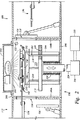
[0034]図3は、第1の支持プレート160および第2の支持体202の等角図を示す。第1の支持プレート160は、一般的には、複数の支持部材302を含み、この支持部材302は、第1の支持プレート160に対して所定の間隔を置いた関係で基板を維持するように適合される。支持部材302の高さは、一般的には、支持部材302上に載置された基板と支持プレート160との間にロボット136および134のブレードが入り込めるように構成される。オプションとして、ロボット136および134のブレードのための空間を提供するために、通路が、支持部材302間の支持プレート160に形成されてもよい。支持部材302は、更に、基板にひっかき傷をつけ、あるいは、基板を損傷することなく、基板が第1の支持プレート160の平面に平行に移動するのを可能にする。支持部材302は、いろいろなものが考えられるが、低摩擦のパッド、ローラーボール、または、空気軸受であってもよい。図3に示される実施形態においては、支持部材302は、例えば、フルオロポリマーから製造されたプラスチックパッドである。基板を損傷する可能性を最小限に抑制するために、第2の支持体202の先端232も、また、支持部材302を含んでもよい。
FIG. 3 shows an isometric view of the
[0035]第1の支持プレート160は、典型的には、複数のアライメント機構162によって取り囲まれる。アライメント機構162は、支持プレート160に結合されてもよく、あるいは、チャンバー本体102の一部分に結合されてもよい。複数のアライメント機構162は、協働して、支持プレート160に対して予め定められた位置に基板を確実に配置するように構成される。一般的には、アライメント機構の第1の対は、これらの間に、第1の座標軸に沿って基板を位置合わせするように適合され、アライメント機構の第2の対は、これらの間に、第2の座標軸に沿って基板を位置合わせするように適合され、それによって、協働して、基板を予め定められた位置へ移動させる。典型的には、第1の座標は、第2の座標に垂直に配置される。
[0035] The
[0036]図3に示される実施形態においては、第1の対であるアライメント機構304および306は、第1の支持プレート160の第1の角350の隣接する辺に配置され、第2の対であるアライメント機構308および310は、対角的に向かい合った第2の角352の隣接する辺に配置される。アライメント機構の向かい合ったそれぞれの対に含まれる、向かい合ったアライメント機構162(すなわち、306および308、および、304および310)は、反対方向に基板を移動させるように適合され、それによって、基板をこれらの中央に配置する。更にまた、アライメント機構は、典型的には、支持プレート160の中間点からずれた位置に結合されるので、アライメント機構162が、支持プレート160に対して予め定められた位置へ基板を移動させるときに、基板のスキューを補正することができる。あるいは、アライメント機構162は、支持プレート160のそれぞれの辺に沿ってどこにでも配置されてよい(すなわち、支持プレート160の角にではなく)。更に、本発明は、支持プレート160の1つの辺に沿ってただ1つのアライメント機構162を使用することを考察し、このただ1つのアライメント機構162は、基板を位置合わせするために、従来のアライメント装置と協働する。
[0036] In the embodiment shown in FIG. 3, the first pair of alignment features 304 and 306 are located on adjacent sides of the
[0037]図3に示される実施形態においては、第3の対であるアライメント機構312および314、および、第4の対であるアライメント機構316および318が、第1の支持プレート160の第3および第4の対角的な角354および356に配置される。この更なるアライメント機構の対は、第1の支持プレート160上において基板を位置合わせするとき、精度を得るための更なる手段を提供する。
[0037] In the embodiment shown in FIG. 3, a third pair of
[0038]図4は、第1の支持プレート160および一実施形態のアライメント機構304の部分正面図を示す。一実施形態においては、この他のアライメント機構は、同様に適合される。アライメント機構304は、一般的には、アーム404によって本体406に結合された押し込み部材402を含む。本体406は、それを貫通して配置されたシャフト408を有する。シャフト408は、本体406のそれぞれの側に配置された一対の取付ブラケット412によって、第1の支持プレート160に結合される。シャフト408は、アクチュエータ412に結合され、このアクチュエータは、押し込み部材402をシャフト408を中心にして回転させるために、様々な形で作動または駆動されてもよい。アクチュエータ412は、典型的には、コントローラ414に結合される。
[0038] FIG. 4 illustrates a partial front view of the
[0039]コントローラ414は、一般的には、中央処理装置(CPU)420、支援回路418、および、メモリー416を含む。CPU420は、押し込み部材402の動作を制御するための産業機器に使用することができれば、どのような形のコンピュータプロセッサの1つであってもよい。メモリー416は、CPU420に結合される。メモリー416またはコンピュータ可読媒体は、ランダムアクセスメモリー(RAM)、リードオンリーメモリー(ROM)、フロッピーディスク、ハードディスク、または、何らかのこの他の形態のローカルまたはリモートディジタル記憶装置のような、1つかまたはそれ以上の容易に利用することのできるメモリーであってもよい。支援回路418は、CPU420に結合され、一般的な形でプロセッサを支援する。これらの回路は、キャッシュ、電源、クロック回路、入力/出力回路、サブシステム等を含む。
[0039] The
[0040]コントローラ414は、一般的には、アクチュエータ412に信号を提供し、それによって、アクチュエータ412は、シャフト408に回転運動を与える。図4に示される実施形態においては、アクチュエータ412は、サーボ、ステッパー、または、この他の電気モーター、空気モーター、油圧モーターであってもよく、あるいは、この他の装置または機構の組み合わせが考えられるが、例えば、シャフト408に軸をずらして結合されたリニアアクチュエータのような、シャフト408を回転させることのできる回転ソレノイドであってもよい。
[0040] The
[0041]図5A〜図5Cを参照すると、アクチュエータ412が、シャフト408を回転させると、押し込み部材402は、第1の支持プレート160の中央領域に向かって移動する。押し込み部材402は、一般的には、基板106にひっかき傷をつけ、基板106を損傷し、あるいは、基板106を汚染することのない材料から製造される。一実施形態においては、押し込み部材402は、例えば、フルオロポリマーのようなポリマーから製造される。
[0041] Referring to FIGS. 5A-5C, when the
[0042]押し込み部材402は、一般的には、面502を含み、アライメント機構304を回転させると、この面502は、ずれた基板106に接触する。面502は、一般的には、基板106を第1の方向に予め定められた位置まで押し込む。典型的には、第1の方向512は、シャフト408の回転軸514および接線面502に垂直である。一実施形態においては、押し込み部材402が回転するときに、基板106が持ち上がるのを防止するために、面502は、凹面であり、それによって、基板が、間隔部材302上を第1の方向512へ移動することを保証する。押し込み部材402を支持プレート160の中央に向かって回転させた後、アクチュエータ412は、一般的には、アライメント機構304を図5Aに示される位置へ戻し、この位置において、押し込み部材402は、基板の搬送を容易にするために、基板から離れている。
[0042] The
[0043]押し込み部材402は、更に、中心軸506を中心にして回転するように構成され、この中心軸506は、典型的には、回転軸514に垂直に配置される。この押し込み部材402が回転できる能力は、基板106が、押し込み部材402に対して横方向へ移動するのを容易にする。したがって、基板は、押し込み部材402上を接線方向へ移動することができ、面502は、一般的には、中心軸506を中心にして対称となるように構成される。例えば、アライメントプロセス中に、隣接するアライメント機構306(図5Cに示されるように)が、同様に、基板に接触していれば(すなわち、それぞれのアライメント機構304および306が、支持プレート160の中央に向かって回転している)、基板106は、2つの方向へ同時に動かされる。押し込み部材402は、それの軸506を中心にして回転することができるので、アライメント機構306によって加えられる力によって、基板は、過度に大きな摩擦または微粒子を発生させることなく、押し込み部材402に接触しながら横方向へ移動することができる。同様に、アライメント機構306は、押し込み部材522を有し、この押し込み部材522は、それの軸を中心にして回転し、この押し込み部材522に接触している基板が、横方向へ移動するのを可能にする。したがって、押し込み部材402および522によって、基板は、一方の方向へ横に移動することができ、それと同時に、基板は、典型的には垂直なもう一方の方向へも移動することができる。
[0043] The
[0044]一実施形態においては、留め具508が、押し込み部材402の軸506に沿って形成された孔504の中に配置され、アーム404内に形成されたねじ孔510内にねじ込まれ、押し込み部材402が回転するのを容易にする。あるいは、押し込み部材402を回転可能に結合するためのこの他の構成が、使用されてもよい。同様に、押し込み部材522が、アライメント機構306に結合される。
[0044] In one embodiment, the
[0045]基板106を予め定められた位置に配置するために、軸514を中心にした押し込み部材402の回転または行程は、典型的には、機械的または電子的に制限される。例えば、コントローラ414が、押し込み部材402の回転を予め定められた角度に制限するように、アクチュエータ412に命令を送信してもよい。図5Aおよび図5Bに示される実施形態においては、機械的な停止装置524が、アライメント機構304の回転角を制限する位置に配置される。例えば、停止装置524は、支持プレート160に対して予め定められた角度でアーム404を停止させる場所において、支持プレート160に結合されてもよい。あるいは、押し込み部材402の運動を制御および/または制限するためのこの他の構成および方法が、使用されてもよい。
[0045] To place the
[0046]図6は、異なる実施形態のアライメント機構602を有するロードロックチャンバー600の部分断面図である。ロードロックチャンバー600は、一般的には、上述したロードロックチャンバー100に類似し、また、一般的には、少なくとも4つのアライメント機構を含み、それらは、チャンバー600内に配置された基板のそれぞれの辺に沿って配置され、これらの中のアライメント機構602だけが、図6に示される。一般的には、図3を参照して説明したように、アライメント機構602の少なくとも2つの対が、基板604を対角的に横断する2つの角に使用される。オプションとして、更なるアライメント機構602が、基板602のいずれかの縁部に沿って使用されてもよく、および/または、基板を対角的に横断する2つの角に使用されてもよい。
[0046] FIG. 6 is a partial cross-sectional view of a
[0047]アライメント機構602は、一般的には、アーム606によってシャフト608に結合された押し込み部材604を含む。取付ブラケット608が、シャフト608を支持プレート160に結合する。一般的には、アクチュエータ614が、ずれた基板を第1の方向630へ移動させるために、アライメント機構602と連結する。典型的には、第1の方向630は、シャフト608に垂直であり、このシャフト608を中心にして、アーム606および押し込み部材604が、回転する。
[0047] The
[0048]図6に示される実施形態においては、アクチュエータ614は、冷却プレート214およびそれに結合された作動フィンガー616を含む。冷却プレート214が、リフト機構216によって持ち上げられるとき、作動フィンガー616は、アライメント機構602に接触し、アライメント機構602は、押し込み部材604を支持プレート160の中央に向かって回転させる。作動フィンガー616とアライメント機構602との間における微粒子の発生を最小限に抑制するために、冷却プレート214が、持ち上げられるとき、作動フィンガー616が、ローラー612の上に載ることのできる位置において、ローラー612が、アーム606に結合される。微粒子の発生を更に少なくするために、ローラー612は、典型的には、例えば、フルオロポリマーのようなプラスチックから製造され、作動フィンガー616と接触しているときに回転する。
[0048] In the embodiment shown in FIG. 6,
[0049]押し込み部材604の運動の行程および速度を制御するために、作動フィンガー616の垂直な第1の部分620は、作動中にローラー612に係合する付形面618を有する。付形面618は、直線または曲線であってもよく、あるいは、予め定められた角度だけ回転するときに予め定められた1つかまたは複数の速度で押し込み部材604を移動させるように構成される複雑な形状を有してもよい。作動フィンガー616の第2の部分622は、冷却プレート214内に形成されたねじ孔628にねじ込まれる留め具626を収容するスロット624を含む。スロット624によって、支持プレート160に対する作動フィンガー616の位置を調節することができ、すなわち、付形面618とローラー612との相対的な位置を調節することができ、それによって、押し込み部材の動作の調節範囲を広くすることができる。
[0049] To control the stroke and speed of movement of the
[0050]図7は、一実施形態のアライメント機構602の分解図を示す。アライメント機構602のアーム404は、一般的には、中央部分706によって結合された第1のフランジ702と第2のフランジ704とを含む。中央部分706は、それに回転可能に結合された押し込み部材604を有する。第2のフランジ704は、ローラー612に隠れているが、第1のフランジ702に実質的に類似するものである。第1および第2のフランジ702および704は、それぞれ、そこに形成された第1の孔708および第2の孔710を有する。第1の孔708は、ローラー612に回転軸を提供するダウエルピン712を収容するように適合される。ローラー612の回転軸は、一般的には、シャフト608に平行であり、かつ、押し込み部材604の回転軸に垂直である。第2の孔710は、一般的には、アーム604が回転するのを可能にするシャフト608を収容する。
[0050] FIG. 7 shows an exploded view of an
[0051]取付ブラケット610は、一般的には、基部714を含み、この基部714は、そこから“U字形”をなして延びる第1および第2の部材716および718を有する。基部714は、それを貫通して形成された複数の取付孔720を有し、この取付孔720は、取付ブラケット610を支持プレート160に結合するのを助ける。図7に示される実施形態においては、一対の留め具722が、孔720の中を通り、支持プレート160に形成されたねじ孔724にねじ込まれる。
[0051] Mounting bracket 610 generally includes a base 714 having first and
[0052]取付ブラケット610のそれぞれの部材716および718は、シャフト608を収容する開口726を含む。図7に示される実施形態においては、シャフト608は、一対のシャフト要素728を備える。シャフト要素728のそれぞれは、ねじ付き端部730およびロッド端部732を有する。シャフト要素728のねじ付き端部730は、取付ブラケット610のそれぞれの部材716および718に係合し、ロッド端部732が孔726から突き出るのを可能にする。ロッド端部732は、それぞれ、アーム404の第1および第2のフランジ702および704の第2の孔710内に配置され、それによって、アーム404が取付ブラケット410に対して回転するのを可能にする。
[0052] Each
[0053]更に、付勢部材734が、フランジ702および704の一方とアーム606との間に配置される。付勢部材734は、一般的には、押し込み部材604を支持プレート160から遠ざける方向へシャフト608を中心にして回転するように、アーム606を付勢する。したがって、作動フィンガー616が、移動し、ローラー612に接触したときに、付勢部材734は、ローラー612と付形面618とがぴったりと接触することを保証し、それによって、この結果として得られる押し込み部材604の動作は、予め定められた範囲および速度を有することになる。更に、付勢部材734によって、押し込み部材604は、アライメントプロセスの後、支持プレート160から遠ざかるように旋回することができ、このために、基板の搬送を妨害しない。一実施形態においては、付勢部材734は、ねじりばねである。
[0053] Further, a biasing
[0054]図8Aおよび図8Bは、非作動状態にあるアライメント機構602、および、基板を第1の方向へ移動させる作動状態にあるアライメント機構602を示す。また、図示しないが、これと同時に、この他のアライメント機構が、同様に、作動され、基板を第2の方向へ移動させ、この結果として、第1の方向への基板の移動とともに、協働して、基板を予め定められた位置へ移動させる。一般的には、基板106は、大気ロボット(図示しない)によって、支持プレート160の支持部材302上に配置される。冷却プレート214およびアクチュエータフィンガー616を備えるアクチュエータ614は、冷却プレート214に結合されたリフト機構214によって、持ち上げられる。アクチュエータフィンガー616が、上方向へ持ち上げられるにつれて、アクチュエータフィンガー616の付形面618が、アライメント機構602のローラー612に接触し、それによって、アライメント機構は、押し込み部材604を支持プレート160の中央に向かって回転させる。基板が、図8Aおよび図8Bに示されるこのアライメント機構の方へずれていれば、押し込み部材604は、基板106に接触し、基板を第1の方向630へ押し込む。支持プレート160のこの他の縁部に沿って配置されたこの他のアライメント機構(図3に類似して示される)が、第1の方向630と異なる第2の方向へ基板を押し込むとき、押し込み部材604は、回転し、それによって、基板は、基板を損傷することなく、あるいは、微粒子を発生させることなく、アライメント機構602に沿って横方向へ、典型的には、第1の方向630に垂直な方向へ移動することができる。この他のアライメント機構との協働相互作用は、基板のずれによって基板を損傷することなく、更なるハンドリングおよび加工を容易にする予め定められた位置に基板を配置する。
[0054] FIGS. 8A and 8B show the
[0055]更に、冷却プレート214は、アライメントプロセス中に搬送チャンバー(図示しない)から戻される加工された基板802に近接した位置へ移動する。この位置において、基板802の冷却が、ロードロックチャンバー600内の独立したアクチュエータまたは制御装置を更に必要とせずに、アライメントプロセスと同時に開始し、アライメントおよび冷却の両方を容易にする。
[0055] Further, the
[0056]図9〜図11は、ロードロックチャンバーに使用することのできる別の実施形態のアライメント機構902を示す。一般的には、少なくとも1つのアライメント機構902が、支持プレート160のそれぞれの辺に結合される(支持プレート160の1つの角の隣接する辺に配置された2つのアライメント機構しか示さない)。それぞれのアライメント機構902は、支持プレート160の中央に向かって線形に移動するように作動させることができる。アライメント機構902は、アクチュエータ904によって動かされる。アクチュエータ904は、一般的には、上述したアクチュエータ616に類似し、冷却プレート214に結合された作動フィンガー906を含む。
[0056] FIGS. 9-11 illustrate another embodiment of an
[0057]アライメント機構902は、一般的には、中央本体910から構成され、この中央本体910は、本体910の支持プレート160に面する側に結合された押し込み部材912と、本体910の反対側に結合されたローラー914とを有する。押し込み部材912は、本体910に取り付けられているように示されるが、それとは異なって、押し込み部材912は、上述した押し込み部材402および406に類似して回転するように適合されてもよい。
[0057] The
[0058]一般的には、複数のガイドが、アライメント機構902を支持プレート160に結合し、それによって、アライメント機構902は、支持プレート160に対して移動することができる。一実施形態においては、ガイドは、一対の肩つきねじ916を含み、このそれぞれは、アライメント機構902に形成された孔918を貫通し、支持プレート160に形成された孔920にねじ込まれる。孔918の支持プレート160に面する側は、ばね922を部分的に収容する座ぐりを含む。ばね922は、一般的には、支持プレート160から遠ざけるようにアライメント機構902を付勢し、押し込み部材904と支持プレート160上に配置された基板との間に十分なクリアランスを提供する。
[0058] In general, a plurality of guides couple the
[0059]一般的には、基板は、冷却プレート214を持ち上げてアライメント機構902を作動させることによって、支持プレート160上に位置合わせされる。作動フィンガー902は、ローラー914を付形面924に接触させ、この付形面924は、アライメント機構902を支持プレート160の中央に向かって移動させる。それぞれのアライメント機構902が、支持プレート160の4つの辺に沿って作動させられると、支持プレート160上に載置された基板は、アライメント機構902によって、基板のずれによって基板を損傷することなく、更なるハンドリングおよび加工を容易にする予め定められた位置へ押し込められる。
[0059] In general, the substrate is aligned on the
[0060]以上、本発明のいくつかの実施形態について説明したが、本発明の基本的な範囲を逸脱することなく、本発明のこの他のおよび更なる実施形態を考え出すことができ、この本発明の範囲は、特許請求の範囲に規定される。 [0060] While several embodiments of the invention have been described above, other and further embodiments of the invention may be devised without departing from the basic scope thereof. The scope of the invention is defined in the claims.
100…ロードロックチャンバー、102…本体、104A、104B…壁、106…基板、108…搬送チャンバー、110…内部空間、112…ファクトリインタフェース、114、118…ポート、116、120…スリットバルブ、122…ベントポート、124…真空ポート、126、128…バルブ、130…真空ポンプ、132…プロセスチャンバー、134…真空ロボット、136…大気ロボット、138…基板収容カセット、140…ベイ、150…プロセスシステム、160…支持プレート、162…基板アライメント機構、
DESCRIPTION OF
Claims (26)
前記基板を支持するように適合される第1の面と、前記第1の面の一部分との境界を規定する第1の縁部とを有する支持プレートと、
前記第1の縁部の近くに回転可能に配置された第1の本体と、
前記第1の本体に半径方向に結合され、且つ前記第1の本体が回転するときに前記基板を前記第1の面に平行な第1の方向へ移動させるように適合された第1の押し込み部材であって、前記第1の押し込み部材は、前記第1の本体の回転により画成された第1の回転軸と、前記第1の回転軸と異なる向きの第2の回転軸を有する、前記第1の押し込み部材と、
を備える、前記装置。An apparatus for supporting a substrate,
A support plate having a first surface adapted to support the substrate and a first edge defining a boundary with a portion of the first surface ;
A first body rotatably disposed near the first edge;
A first indent coupled to the first body in a radial direction and adapted to move the substrate in a first direction parallel to the first surface when the first body rotates. The first pushing member has a first rotating shaft defined by rotation of the first main body and a second rotating shaft in a direction different from the first rotating shaft; The first pushing member;
Comprising the apparatus.
貫通して第1の孔が形成された第1のフランジと、
貫通して第2の孔が形成された第2のフランジと、
前記第1および第2のフランジに結合された中央部分と、
前記第1および第2のフランジ間に配置されたローラーであって、前記第1の回転軸と平行に向けられた第3の回転軸を有し、前記第3の回転軸が、前記第1の回転軸と前記中央部分との間に画成される、前記ローラーと、
を更に備え、
前記第1の孔と前記第2の孔は、前記第1の回転軸と同軸に整列されている、請求項1に記載の装置。 The first body comprises:
A first flange having a first hole formed therethrough;
A second flange having a second hole formed therethrough;
A central portion coupled to the first and second flanges;
A first and second arranged rollers between the flanges, before SL has a third axis of rotation was found oriented parallel to the first axis of rotation, the third axis of rotation, said The roller defined between a first axis of rotation and the central portion;
Further comprising
It said first hole and said second hole is pre SL aligned with the first axis of rotation coaxial Apparatus according to claim 1.
前記冷却プレートに結合され、且つ前記冷却プレートが前記第1の本体に対して移動するときに前記ローラーを移動させるように適合されている作動フィンガーと、
を更に備える、請求項3に記載の装置。A cooling plate;
An actuating finger coupled to the cooling plate and adapted to move the roller as the cooling plate moves relative to the first body;
The apparatus of claim 3 , further comprising:
前記第2の本体に半径方向に結合され、且つ前記第2の本体が回転するときに前記基板を前記第1の方向と異なる第2の方向へ移動させるように適合されている第2の押し込み部材と、
を更に備える、請求項1に記載の装置。A second body rotatably disposed near a second edge of the support plate, wherein the second edge is disposed adjacent to the first edge. The body,
Coupled to said radially second body and the second body said substrate adapted to have a second so as to move in a second direction different from the first direction when rotating A pushing member;
The apparatus of claim 1, further comprising:
前記第3の本体に半径方向に結合され、且つ前記第3の本体が回転するときに前記基板を前記第1の方向と反対の方向へ移動させるように適合されている第3の押し込み部材と、
前記支持プレートの第4の縁部の近くに回転可能に配置された第4の本体であって、前記第4の縁部が、前記第2の縁部の反対側に配置された第4の本体と、
前記第4の本体に半径方向に結合され、且つ前記第4の本体が回転するときに前記基板を前記第2の方向と反対の方向へ移動させるように適合されている第4の押し込み部材と、
を更に備える、請求項6に記載の装置。A third body rotatably disposed near a third edge of the support plate, wherein the third edge is disposed adjacent to the second edge and the first A third body on the opposite side of the edge of the
A third pusher member coupled radially to the third body and adapted to move the substrate in a direction opposite to the first direction when the third body rotates. ,
A fourth body rotatably disposed near a fourth edge of the support plate, wherein the fourth edge is disposed on an opposite side of the second edge; The body,
A fourth pushing member coupled to the fourth body in a radial direction and adapted to move the substrate in a direction opposite to the second direction when the fourth body rotates. ,
The apparatus of claim 6 , further comprising:
前記基板を支持するように適合される第1の面と、前記第1の面の一部分との境界を規定する第1の縁部とを有する支持プレートであって、前記支持プレートは前記第1の面に対し垂直に突き出た中心線に対し固定されている、前記支持プレートと、
前記第1の縁部の近くにあり、前記支持プレートの平面に対し平行な第1の回転軸を中心として回転可能な第1の本体と、
前記第1の本体に半径方向に結合され、且つ前記第1の本体が回転するときに前記基板を前記第1の面に平行な第1の方向へ押し込むように適合されている第1の押し込み部材であって、前記第1の押し込み部材は、前記第1の回転軸と、前記支持プレートの前記中心線と選択的に平行な第2の回転軸とを有する、前記第1の押し込み部材と、
を備える、前記装置。An apparatus for supporting a substrate ,
A support plate having a first surface adapted to support the substrate and a first edge defining a boundary with a portion of the first surface , wherein the support plate is the first surface. The support plate being fixed with respect to a center line protruding perpendicular to the surface of
A first body near the first edge and rotatable about a first axis of rotation parallel to the plane of the support plate;
A first push that is radially coupled to the first body and adapted to push the substrate in a first direction parallel to the first surface when the first body rotates. The first push-in member having the first rotary shaft and a second rotary shaft selectively parallel to the center line of the support plate; ,
Comprising the apparatus.
貫通して第1の孔が形成された第1のフランジと、
貫通して第2の孔が形成された第2のフランジと、
前記第1のフランジおよび前記第2のフランジに結合された中央部分と、
前記第1および第2のフランジ間に配置されたローラーであって、前記第1の回転軸に平行に向けられた第3の回転軸を有し、前記第3の回転軸が、前記第1の回転軸と前記中央部分との間に画成される、前記ローラーと、
を更に備え、
前記第1の孔と前記第2の孔は、前記第1の回転軸と同軸に整列されている、請求項8記載の装置。The first body includes
A first flange having a first hole formed therethrough;
A second flange having a second hole formed therethrough;
A central portion coupled to the first flange and the second flange;
A first and second arranged rollers between the flanges, before SL has a third rotational axis oriented parallel to the first axis of rotation, the third axis of rotation, said first The roller defined between the rotational axis of 1 and the central portion;
Further comprising
It said first hole and said second hole is pre SL aligned in a first rotational shaft and the shaft, according to claim 8.
前記冷却プレートに結合され、且つ前記冷却プレートが前記第1の本体に対して移動するときに前記ローラーを押し込むように適合される作動フィンガーと、
を更に備える、請求項11に記載の装置。A cooling plate;
An actuation finger coupled to the cooling plate and adapted to push the roller as the cooling plate moves relative to the first body;
The apparatus of claim 11 , further comprising:
前記第2の本体に半径方向に結合され、且つ前記第2の本体が回転するときに前記基板を前記第1の方向と異なる第2の方向へ押し込むように適合される第2の押し込み部材と、
を更に備える、請求項8に記載の装置。A second body rotatably disposed near a second edge of the support plate, wherein the second edge is disposed adjacent to the first edge. The body,
A second pushing member coupled radially to the second body and adapted to push the substrate in a second direction different from the first direction when the second body rotates; ,
The apparatus of claim 8 , further comprising:
前記第3の本体に半径方向に結合され、且つ前記第3の本体が回転するときに前記基板を前記第1の方向と反対の方向へ押し込むように適合される第3の押し込み部材と、
前記支持プレートの第4の縁部の近くに回転可能に配置された第4の本体であって、前記第4の縁部が、前記第2の縁部の反対側に配置された第4の本体と、
前記第4の本体に半径方向に結合され、且つ前記第4の本体が回転するときに前記基板を前記第2の方向と反対の方向へ押し込むように適合される第4の押し込み部材と、
を更に備える、請求項14に記載の装置。A third body rotatably disposed near a third edge of the support plate, wherein the third edge is disposed adjacent to the second edge and the first A third body on the opposite side of the edge of the
A third pusher member coupled radially to the third body and adapted to push the substrate in a direction opposite to the first direction when the third body rotates;
A fourth body rotatably disposed near a fourth edge of the support plate, wherein the fourth edge is disposed on an opposite side of the second edge; The body,
A fourth pushing member coupled radially to the fourth body and adapted to push the substrate in a direction opposite to the second direction when the fourth body rotates;
15. The apparatus of claim 14 , further comprising:
上部に基板を支持するように適合され、貫通して垂直に伸びる中心線に対し回転可能に固定された支持プレートと、
第1の回転軸と第2の回転軸を有する第1の押し込み部材であって、前記第1の回転軸は前記第2の回転軸に対し垂直に向けられ、第1の押し込み部材は、第1の方向に前記基板を押し込むように適合されている、前記第1の押し込み部材と、
第3の回転軸と第4の回転軸を有する第2の押し込み部材であって、前記第3の回転軸は、前記第1の回転軸に対し平行に、前記第4の回転軸に対し垂直に向けられ、前記第2の押し込み部材は、前記第1の方向とは反対の第2の方向に前記基板を押し込むように適合されている、前記第2の押し込み部材と、
を備える、前記装置。An apparatus for supporting a substrate ,
A support plate adapted to support the substrate on the top and fixed rotatably about a center line extending vertically therethrough ;
A first pushing member having a first rotation axis and the second rotation axis, the first axis of rotation is oriented perpendicular to the second axis of rotation, the first pushing Write-member The first pusher member adapted to push the substrate in a first direction ;
A second push-in member having a third rotation axis and a fourth rotation axis, wherein the third rotation axis is parallel to the first rotation axis and perpendicular to the fourth rotation axis; The second pusher member is adapted to push the substrate in a second direction opposite to the first direction; and
Comprising the apparatus.
前記第5の回転軸に対し平行に配置された第7の回転軸と、前記第7の回転軸に対し垂直に向けられた第8の回転軸を有する第4の押し込み部材であって、前記第1,第3,第5,第7の回転軸が、単一平面内に横たわり、前記第4の押し込み部材は、前記第3の方向と反対の第4の方向に前記基板を押し込むように適合されている、前記第4の押し込み部材と、
を更に備える、請求項16記載の装置。A third pushing member having a fifth rotating shaft arranged perpendicular to the first rotating shaft and a sixth rotating shaft oriented perpendicular to the fifth rotating shaft; The third pusher member is adapted to push the substrate in a third direction ; and
A fourth pushing member having a seventh rotating shaft arranged in parallel to the fifth rotating shaft and an eighth rotating shaft oriented perpendicular to the seventh rotating shaft, The first, third, fifth , and seventh rotation axes lie in a single plane, and the fourth pushing member pushes the substrate in a fourth direction opposite to the third direction. Said fourth pushing member being adapted ,
The apparatus of claim 16 , further comprising:
基板支持体と、
第1のアクチュエータと、
前記第1のアクチュエータにより前記基板支持体に向かって移動可能であり、第1の回転軸を有する、第1の押し込み部材と、
第2のアクチュエータと、
前記第2のアクチュエータにより前記基板支持体に向かって移動可能な第2の押し込み部材とを備え、
第2の押し込み部材は、前記第1の回転軸に垂直な第2の回転軸上で前記第1の押し込み部材を回転させる方向で、前記基板支持体上で基板を変位させるように構成されている、前記装置。An apparatus for supporting a substrate ,
A substrate support;
A first actuator;
A first pushing member that is movable toward the substrate support by the first actuator and has a first rotation axis ;
A second actuator ;
A second pushing member movable toward the substrate support by the second actuator ,
The second pushing member is configured to displace the substrate on the substrate support in a direction in which the first pushing member is rotated on a second rotation axis perpendicular to the first rotation axis. that, said device.
基板支持体と、
前記基板支持体の上面に対して、それぞれ垂直及び平行に選択的に回転される第1の回転軸と第2の回転軸を有する、第1の押し込み部材と、
前記基板支持体の前記上面に対して、それぞれ垂直及び平行に選択的に回転される第3の回転軸と第4の回転軸を有する、第2の押し込み部材と、
を備える、前記装置。An apparatus for supporting a substrate ,
A substrate support,
And to the upper surface of the substrate support, each having a first rotary shaft and second rotary shaft which is selectively rotated vertically and parallel, and the first pushing member,
And with respect to the upper surface of the substrate support, each having a third axis of rotation and a fourth rotary shaft which is selectively rotated vertically and parallel, and a second pushing member,
Comprising the apparatus.
第1の基板搬送ポートと第2の基板搬送ポートを有するチャンバー本体と、
前記チャンバー本体内部に配置され、前記基板を支持するように適合された第1の面を有する、支持プレートと、
第1の回転軸と、前記第1の回転軸に対し垂直な第2の回転軸とを有する第1の押し込み部材であって、前記第1の押し込み部材が前記第1の回転軸の周りに回転されるとき、第1の方向に前記基板を押し込むように適合されている、前記第1の押し込み部材と、
を備える、前記ロードロックチャンバー。A load lock chamber over that transports the substrate between the first environment and a second environment,
A chamber over body having a first substrate transfer port and a second substrate transfer port,
Wherein disposed within the chamber over the body, having a first surface adapted to support the substrate, a supporting plate,
A first pushing member having a first rotating shaft and a second rotating shaft perpendicular to the first rotating shaft, wherein the first pushing member is arranged around the first rotating shaft. The first pusher member adapted to push the substrate in a first direction when rotated ;
The equipped, the load lock chamber over.
貫通して第1の孔が形成された第1のフランジと、
貫通して第2の孔が形成された第2のフランジと、
前記第1および第2のフランジに結合された中央部分と、
前記第1および第2のフランジ間に配置されたローラーであって、前記第1の回転軸に平行に向けられた第3の回転軸を有し、前記第3の回転軸が、前記第1の回転軸と前記中央部分との間に画成される、前記ローラーと、
を更に備え、
前記第1の孔と前記第2の孔は、前記第1の回転軸と同軸に整列されている、請求項25に記載のロードロックチャンバー。The body is
A first flange having a first hole formed therethrough;
A second flange having a second hole formed therethrough;
A central portion coupled to the first and second flanges;
A first and second arranged rollers between the flanges, before SL has a third axis of rotation was found oriented parallel to the first axis of rotation, the third axis of rotation, said The roller defined between a first axis of rotation and the central portion;
Further comprising
The first hole and the second hole, the first rotational shaft and is coaxially aligned, the load lock chamber of claim 25.
Applications Claiming Priority (2)
| Application Number | Priority Date | Filing Date | Title |
|---|---|---|---|
| US10/084,762 US6824343B2 (en) | 2002-02-22 | 2002-02-22 | Substrate support |
| PCT/US2003/004885 WO2003073479A1 (en) | 2002-02-22 | 2003-02-18 | Substrate support |
Publications (3)
| Publication Number | Publication Date |
|---|---|
| JP2005518674A JP2005518674A (en) | 2005-06-23 |
| JP2005518674A5 JP2005518674A5 (en) | 2006-01-05 |
| JP4290561B2 true JP4290561B2 (en) | 2009-07-08 |
Family
ID=27753531
Family Applications (1)
| Application Number | Title | Priority Date | Filing Date |
|---|---|---|---|
| JP2003572077A Expired - Lifetime JP4290561B2 (en) | 2002-02-22 | 2003-02-18 | Substrate support |
Country Status (7)
| Country | Link |
|---|---|
| US (2) | US6824343B2 (en) |
| EP (1) | EP1485946B1 (en) |
| JP (1) | JP4290561B2 (en) |
| KR (1) | KR100636491B1 (en) |
| CN (1) | CN100413017C (en) |
| TW (1) | TWI279876B (en) |
| WO (1) | WO2003073479A1 (en) |
Families Citing this family (43)
| Publication number | Priority date | Publication date | Assignee | Title |
|---|---|---|---|---|
| US6824343B2 (en) * | 2002-02-22 | 2004-11-30 | Applied Materials, Inc. | Substrate support |
| US20050037485A1 (en) * | 2003-06-05 | 2005-02-17 | Rodgers Seth T. | System and method for process automation |
| DE102004036435B4 (en) * | 2003-08-07 | 2007-08-30 | Nanophotonics Ag | Holding device for disc-shaped objects |
| US7207766B2 (en) * | 2003-10-20 | 2007-04-24 | Applied Materials, Inc. | Load lock chamber for large area substrate processing system |
| US20050160992A1 (en) * | 2004-01-28 | 2005-07-28 | Applied Materials, Inc. | Substrate gripping apparatus |
| US7018161B2 (en) * | 2004-06-18 | 2006-03-28 | Blueprint Automation B.V. | Suction head |
| US7144813B2 (en) * | 2004-11-12 | 2006-12-05 | Semitool, Inc. | Method and apparatus for thermally processing microelectronic workpieces |
| US7440091B2 (en) * | 2004-10-26 | 2008-10-21 | Applied Materials, Inc. | Sensors for dynamically detecting substrate breakage and misalignment of a moving substrate |
| US7547181B2 (en) * | 2004-11-15 | 2009-06-16 | Dainippon Screen Mfg. Co., Ltd. | Substrate position correcting method and apparatus using either substrate radius or center of rotation correction adjustment sum |
| KR100710598B1 (en) * | 2004-12-08 | 2007-04-24 | 주식회사 에이디피엔지니어링 | Apparatus for fabricating flat panel display |
| KR20070013134A (en) | 2005-07-25 | 2007-01-30 | 삼성전자주식회사 | Apparatus and method for manufacturing display device substrate |
| KR100749755B1 (en) * | 2006-02-10 | 2007-08-16 | 주식회사 싸이맥스 | Apparatus for processing semiconductor wafer |
| JP4098338B2 (en) * | 2006-07-20 | 2008-06-11 | 川崎重工業株式会社 | Wafer transfer device and substrate transfer device |
| KR100829923B1 (en) * | 2006-08-30 | 2008-05-16 | 세메스 주식회사 | Spin head and method using the same for treating substrate |
| EP2095412B1 (en) * | 2006-12-14 | 2016-06-29 | Kemet Japan CO., LTD. | Disc holding apparatus and defect/foreign material detecting apparatus |
| US20080203083A1 (en) * | 2007-02-28 | 2008-08-28 | Wirth Paul Z | Single wafer anneal processor |
| US8234771B2 (en) * | 2007-03-21 | 2012-08-07 | General Electric Company | Method and system for machining an array of components |
| CN101663744B (en) * | 2007-04-23 | 2012-08-15 | 株式会社爱发科 | Supporting member, carrier and supporting method |
| TW200908363A (en) * | 2007-07-24 | 2009-02-16 | Applied Materials Inc | Apparatuses and methods of substrate temperature control during thin film solar manufacturing |
| US8276959B2 (en) | 2008-08-08 | 2012-10-02 | Applied Materials, Inc. | Magnetic pad for end-effectors |
| KR101111399B1 (en) * | 2009-02-09 | 2012-02-24 | 주식회사 싸이맥스 | Loadlock chamber performing a wafer transmission and a heat treatment simultaneously |
| JP5501688B2 (en) * | 2009-07-30 | 2014-05-28 | 東京エレクトロン株式会社 | Substrate alignment mechanism, vacuum prechamber and substrate processing system using the same |
| KR20110019511A (en) * | 2009-08-20 | 2011-02-28 | 삼성전자주식회사 | Apparatus for locking a magazine |
| WO2011096208A1 (en) | 2010-02-05 | 2011-08-11 | 東京エレクトロン株式会社 | Substrate holder, substrate transfer apparatus, and substrate processing apparatus |
| KR101013019B1 (en) * | 2010-06-21 | 2011-02-14 | 김정태 | Wafer transfer system and transfer method |
| US9371584B2 (en) * | 2011-03-09 | 2016-06-21 | Applied Materials, Inc. | Processing chamber and method for centering a substrate therein |
| US9421617B2 (en) | 2011-06-22 | 2016-08-23 | Tel Nexx, Inc. | Substrate holder |
| US8967935B2 (en) | 2011-07-06 | 2015-03-03 | Tel Nexx, Inc. | Substrate loader and unloader |
| US9082799B2 (en) * | 2012-09-20 | 2015-07-14 | Varian Semiconductor Equipment Associates, Inc. | System and method for 2D workpiece alignment |
| KR101404987B1 (en) * | 2012-10-29 | 2014-06-10 | 주식회사 선익시스템 | Cooling chamber for Glass holder of In-line Deposition system |
| KR101863473B1 (en) * | 2013-12-26 | 2018-05-31 | 가와사끼 쥬고교 가부시끼 가이샤 | End effector and substrate transfer robot |
| CN105575868B (en) * | 2014-11-10 | 2018-12-07 | 上海理想万里晖薄膜设备有限公司 | Substrate calibration method and apparatus |
| JP6535187B2 (en) * | 2015-03-10 | 2019-06-26 | 株式会社荏原製作所 | Substrate transfer hand |
| CN107534000B (en) * | 2015-04-20 | 2021-12-17 | 应用材料公司 | Buffer chamber wafer heating mechanism and support robot |
| US9929029B2 (en) * | 2015-10-15 | 2018-03-27 | Applied Materials, Inc. | Substrate carrier system |
| CN105177509B (en) * | 2015-10-16 | 2017-08-11 | 京东方科技集团股份有限公司 | A kind of backboard clamp device, alignment device and evaporated device |
| CN108352289B (en) * | 2015-11-20 | 2019-10-29 | 株式会社岛津制作所 | Vacuum treatment installation and mass spectrometer |
| US10121655B2 (en) | 2015-11-20 | 2018-11-06 | Applied Materials, Inc. | Lateral plasma/radical source |
| JP6493339B2 (en) * | 2016-08-26 | 2019-04-03 | 村田機械株式会社 | Transport container and method for transferring contents |
| CN107841727A (en) * | 2017-12-15 | 2018-03-27 | 北京创昱科技有限公司 | A kind of cooling component and vacuum coating equipment |
| CN110970344A (en) * | 2018-10-01 | 2020-04-07 | Asm Ip控股有限公司 | Substrate holding apparatus, system including the same, and method of using the same |
| JP7280132B2 (en) * | 2019-07-12 | 2023-05-23 | 株式会社アルバック | Vacuum chamber and substrate processing equipment |
| GB201913356D0 (en) * | 2019-09-16 | 2019-10-30 | Spts Technologies Ltd | Wafer processing system |
Family Cites Families (60)
| Publication number | Priority date | Publication date | Assignee | Title |
|---|---|---|---|---|
| FR2302975A1 (en) * | 1975-03-04 | 1976-10-01 | Saint Gobain | CENTERING DEVICE FOR SHEETS OF GLASS ON THE PLATE OF A MACHINE |
| US4347927A (en) * | 1980-06-23 | 1982-09-07 | Libbey-Owens-Ford Company | Sheet aligning apparatus |
| US5374147A (en) * | 1982-07-29 | 1994-12-20 | Tokyo Electron Limited | Transfer device for transferring a substrate |
| JP2855046B2 (en) | 1993-03-31 | 1999-02-10 | 大日本スクリーン製造株式会社 | Substrate rotation holding device for rotary substrate processing equipment |
| US4655584A (en) * | 1984-05-11 | 1987-04-07 | Nippon Kogaku K. K. | Substrate positioning apparatus |
| JPS61214445A (en) | 1985-03-19 | 1986-09-24 | Fujitsu Ltd | Wafer positioning mechanism |
| US4621797A (en) * | 1985-10-10 | 1986-11-11 | Rca Corporation | Device for orienting an object on a flat surface |
| US4764076A (en) * | 1986-04-17 | 1988-08-16 | Varian Associates, Inc. | Valve incorporating wafer handling arm |
| US4788994A (en) | 1986-08-13 | 1988-12-06 | Dainippon Screen Mfg. Co. | Wafer holding mechanism |
| JPS63124543A (en) | 1986-11-14 | 1988-05-28 | Hitachi Electronics Eng Co Ltd | Plate chucking mechanism |
| US4784377A (en) * | 1986-12-23 | 1988-11-15 | Northern Telecom Limited | Apparatus for locating and supporting ceramic substrates |
| US5040484A (en) * | 1987-05-04 | 1991-08-20 | Varian Associates, Inc. | Apparatus for retaining wafers |
| US4817556A (en) | 1987-05-04 | 1989-04-04 | Varian Associates, Inc. | Apparatus for retaining wafers |
| JPH01242989A (en) * | 1988-03-24 | 1989-09-27 | Kazuya Hirose | Longitudinal and lateral moving and swiveling mechanism for table |
| US4898639A (en) * | 1989-04-14 | 1990-02-06 | Bjorne Enterprises, Inc. | Wafer retention device |
| JP2523177B2 (en) * | 1989-04-28 | 1996-08-07 | 日本写真印刷株式会社 | Positioning table |
| JPH0613222Y2 (en) * | 1989-07-31 | 1994-04-06 | セントラル硝子株式会社 | Plate glass positioning device |
| US5192087A (en) | 1990-10-02 | 1993-03-09 | Nippon Steel Corporation | Device for supporting a wafer |
| US5173029A (en) * | 1991-07-16 | 1992-12-22 | Toledo Automated Concepts, Inc. | Glass sheet positioning device |
| JPH0590238A (en) | 1991-09-27 | 1993-04-09 | Dainippon Screen Mfg Co Ltd | Substrate rotary holding jig of pivoted substrate treating device |
| JP3139155B2 (en) * | 1992-07-29 | 2001-02-26 | 東京エレクトロン株式会社 | Vacuum processing equipment |
| US5636960A (en) * | 1992-07-29 | 1997-06-10 | Tokyo Electron Limited | Apparatus for detecting and aligning a substrate |
| JP3335983B2 (en) | 1993-02-26 | 2002-10-21 | 東京エレクトロン株式会社 | LCD glass substrate alignment mechanism and vacuum processing device |
| US5378215A (en) | 1993-05-14 | 1995-01-03 | Harkins; Robert L. | Rehabilitation apparatus for ambulatory patients |
| US5636980A (en) | 1994-04-12 | 1997-06-10 | Halliburton Company | Burner apparatus |
| US5566466A (en) * | 1994-07-01 | 1996-10-22 | Ontrak Systems, Inc. | Spindle assembly with improved wafer holder |
| US5505438A (en) * | 1994-11-30 | 1996-04-09 | Caterpillar Inc. | Work piece locating apparatus |
| US5538231A (en) * | 1994-11-30 | 1996-07-23 | Caterpillar Inc. | Apparatus for locating a workpiece on a burn table |
| US5579718A (en) * | 1995-03-31 | 1996-12-03 | Applied Materials, Inc. | Slit valve door |
| US5630269A (en) * | 1995-06-19 | 1997-05-20 | General Motors Corporation | Method for fixturing abutted sheet metal parts for welding |
| US5853214A (en) | 1995-11-27 | 1998-12-29 | Progressive System Technologies, Inc. | Aligner for a substrate carrier |
| JPH09213772A (en) * | 1996-01-30 | 1997-08-15 | Dainippon Screen Mfg Co Ltd | Board holder |
| US5961107A (en) | 1996-03-06 | 1999-10-05 | Morghen; Manfred A. | Workpiece indexing and clamping system |
| JPH09290890A (en) | 1996-04-25 | 1997-11-11 | Nikon Corp | Wafer carrier |
| US5775000A (en) | 1996-05-13 | 1998-07-07 | Ebara Corporation | Substrate gripper device for spin drying |
| US5851041A (en) * | 1996-06-26 | 1998-12-22 | Ontrak Systems, Inc. | Wafer holder with spindle assembly and wafer holder actuator |
| JP3831043B2 (en) * | 1997-01-24 | 2006-10-11 | 東京エレクトロン株式会社 | Rotation processing device |
| US6045620A (en) | 1997-07-11 | 2000-04-04 | Applied Materials, Inc. | Two-piece slit valve insert for vacuum processing system |
| US5974681A (en) | 1997-09-10 | 1999-11-02 | Speedfam-Ipec Corp. | Apparatus for spin drying a workpiece |
| WO1999018599A2 (en) | 1997-10-03 | 1999-04-15 | Koninklijke Philips Electronics N.V. | Holder for a semiconductor substrate, and method of manufacturing a semiconductor device using such a holder |
| US5897108A (en) | 1998-01-26 | 1999-04-27 | Gordon; Thomas A. | Substrate support system |
| DE19829580A1 (en) | 1998-07-02 | 2000-01-05 | Bosch Gmbh Robert | Mechanical arrangement for lining up substrates for multilayer electronic circuits lines up carrier substrates by moving axes by cage lead screw movement, with centering elements and stops |
| US6485250B2 (en) * | 1998-12-30 | 2002-11-26 | Brooks Automation Inc. | Substrate transport apparatus with multiple arms on a common axis of rotation |
| US6167893B1 (en) | 1999-02-09 | 2001-01-02 | Novellus Systems, Inc. | Dynamic chuck for semiconductor wafer or other substrate |
| US6163015A (en) | 1999-07-21 | 2000-12-19 | Moore Epitaxial, Inc. | Substrate support element |
| US6262582B1 (en) | 1999-10-15 | 2001-07-17 | International Business Machines Corporation | Mechanical fixture for holding electronic devices under test showing adjustments in multiple degrees of freedom |
| TW452917B (en) * | 1999-10-29 | 2001-09-01 | Winbond Electronics Corp | Holder |
| US6544338B1 (en) * | 2000-02-10 | 2003-04-08 | Novellus Systems, Inc. | Inverted hot plate cure module |
| WO2002005331A2 (en) | 2000-07-08 | 2002-01-17 | Applied Materilas, Inc. | Removable gripper pads |
| US6612014B1 (en) * | 2000-07-12 | 2003-09-02 | Applied Materials, Inc. | Dual post centrifugal wafer clip for spin rinse dry unit |
| US6485248B1 (en) * | 2000-10-10 | 2002-11-26 | Applied Materials, Inc. | Multiple wafer lift apparatus and associated method |
| US6692219B2 (en) * | 2000-11-29 | 2004-02-17 | Tokyo Electron Limited | Reduced edge contact wafer handling system and method of retrofitting and using same |
| US6485246B1 (en) * | 2001-07-20 | 2002-11-26 | New Holland North America, Inc. | Apparatus for raising ramps on an implement transporter |
| US6652656B2 (en) * | 2001-07-24 | 2003-11-25 | Tokyo Electron Limited | Semiconductor wafer holding assembly |
| KR100897431B1 (en) * | 2001-11-27 | 2009-05-14 | 도쿄엘렉트론가부시키가이샤 | Liquid processing apparatus and method |
| US6824343B2 (en) * | 2002-02-22 | 2004-11-30 | Applied Materials, Inc. | Substrate support |
| GB2392309B (en) * | 2002-08-22 | 2004-10-27 | Leica Microsys Lithography Ltd | Substrate loading and unloading apparatus |
| US7101253B2 (en) * | 2002-08-27 | 2006-09-05 | Applied Materials Inc. | Load cup for chemical mechanical polishing |
| US7151981B2 (en) * | 2003-02-20 | 2006-12-19 | Applied Materials, Inc. | Methods and apparatus for positioning a substrate relative to a support stage |
| US7104535B2 (en) * | 2003-02-20 | 2006-09-12 | Applied Materials, Inc. | Methods and apparatus for positioning a substrate relative to a support stage |
-
2002
- 2002-02-22 US US10/084,762 patent/US6824343B2/en not_active Expired - Lifetime
-
2003
- 2003-02-18 JP JP2003572077A patent/JP4290561B2/en not_active Expired - Lifetime
- 2003-02-18 WO PCT/US2003/004885 patent/WO2003073479A1/en active IP Right Grant
- 2003-02-18 CN CNB038043955A patent/CN100413017C/en not_active Expired - Fee Related
- 2003-02-18 KR KR1020047013047A patent/KR100636491B1/en active IP Right Grant
- 2003-02-18 EP EP03743151A patent/EP1485946B1/en not_active Expired - Lifetime
- 2003-02-20 TW TW092103577A patent/TWI279876B/en not_active IP Right Cessation
-
2004
- 2004-11-16 US US10/990,094 patent/US7735710B2/en not_active Expired - Fee Related
Also Published As
| Publication number | Publication date |
|---|---|
| CN1639839A (en) | 2005-07-13 |
| EP1485946A1 (en) | 2004-12-15 |
| US20050063800A1 (en) | 2005-03-24 |
| EP1485946B1 (en) | 2007-01-24 |
| CN100413017C (en) | 2008-08-20 |
| KR20040079446A (en) | 2004-09-14 |
| KR100636491B1 (en) | 2006-10-18 |
| WO2003073479A1 (en) | 2003-09-04 |
| TWI279876B (en) | 2007-04-21 |
| US20030161706A1 (en) | 2003-08-28 |
| US6824343B2 (en) | 2004-11-30 |
| US7735710B2 (en) | 2010-06-15 |
| TW200305245A (en) | 2003-10-16 |
| JP2005518674A (en) | 2005-06-23 |
Similar Documents
| Publication | Publication Date | Title |
|---|---|---|
| JP4290561B2 (en) | Substrate support | |
| US7651315B2 (en) | Large area substrate transferring method for aligning with horizontal actuation of lever arm | |
| US7641247B2 (en) | End effector assembly for supporting a substrate | |
| JP5913572B2 (en) | Storage container, shutter opening / closing unit of storage container, and wafer stocker using them | |
| US6827788B2 (en) | Substrate processing device and through-chamber | |
| US6896513B2 (en) | Large area substrate processing system | |
| US6682343B2 (en) | Substrate processing apparatus | |
| US5944475A (en) | Rotated, orthogonal load compatible front-opening interface | |
| US20120063874A1 (en) | Low profile dual arm vacuum robot | |
| WO2002039499A1 (en) | Method of transferring processed body and processing system for processed body | |
| US20030168175A1 (en) | Substrate alignment apparatus | |
| JP2004146714A (en) | Carrying mechanism for workpiece | |
| JP2006073946A (en) | Glass substrate feeder | |
| JP2000054130A (en) | Load-lock chamber and vacuum treating device |
Legal Events
| Date | Code | Title | Description |
|---|---|---|---|
| A521 | Written amendment |
Free format text: JAPANESE INTERMEDIATE CODE: A523 Effective date: 20050824 |
|
| A621 | Written request for application examination |
Free format text: JAPANESE INTERMEDIATE CODE: A621 Effective date: 20050824 |
|
| A131 | Notification of reasons for refusal |
Free format text: JAPANESE INTERMEDIATE CODE: A131 Effective date: 20080520 |
|
| A601 | Written request for extension of time |
Free format text: JAPANESE INTERMEDIATE CODE: A601 Effective date: 20080820 |
|
| A602 | Written permission of extension of time |
Free format text: JAPANESE INTERMEDIATE CODE: A602 Effective date: 20080827 |
|
| A521 | Written amendment |
Free format text: JAPANESE INTERMEDIATE CODE: A523 Effective date: 20080922 |
|
| RD03 | Notification of appointment of power of attorney |
Free format text: JAPANESE INTERMEDIATE CODE: A7423 Effective date: 20080922 |
|
| TRDD | Decision of grant or rejection written | ||
| A01 | Written decision to grant a patent or to grant a registration (utility model) |
Free format text: JAPANESE INTERMEDIATE CODE: A01 Effective date: 20090303 |
|
| A01 | Written decision to grant a patent or to grant a registration (utility model) |
Free format text: JAPANESE INTERMEDIATE CODE: A01 |
|
| A61 | First payment of annual fees (during grant procedure) |
Free format text: JAPANESE INTERMEDIATE CODE: A61 Effective date: 20090401 |
|
| R150 | Certificate of patent or registration of utility model |
Free format text: JAPANESE INTERMEDIATE CODE: R150 |
|
| FPAY | Renewal fee payment (event date is renewal date of database) |
Free format text: PAYMENT UNTIL: 20120410 Year of fee payment: 3 |
|
| FPAY | Renewal fee payment (event date is renewal date of database) |
Free format text: PAYMENT UNTIL: 20120410 Year of fee payment: 3 |
|
| RD02 | Notification of acceptance of power of attorney |
Free format text: JAPANESE INTERMEDIATE CODE: R3D02 |
|
| FPAY | Renewal fee payment (event date is renewal date of database) |
Free format text: PAYMENT UNTIL: 20130410 Year of fee payment: 4 |
|
| FPAY | Renewal fee payment (event date is renewal date of database) |
Free format text: PAYMENT UNTIL: 20140410 Year of fee payment: 5 |
|
| R250 | Receipt of annual fees |
Free format text: JAPANESE INTERMEDIATE CODE: R250 |
|
| R250 | Receipt of annual fees |
Free format text: JAPANESE INTERMEDIATE CODE: R250 |
|
| R250 | Receipt of annual fees |
Free format text: JAPANESE INTERMEDIATE CODE: R250 |
|
| R250 | Receipt of annual fees |
Free format text: JAPANESE INTERMEDIATE CODE: R250 |
|
| R250 | Receipt of annual fees |
Free format text: JAPANESE INTERMEDIATE CODE: R250 |
|
| R250 | Receipt of annual fees |
Free format text: JAPANESE INTERMEDIATE CODE: R250 |