JP4290281B2 - Absolute sensor - Google Patents
Absolute sensor Download PDFInfo
- Publication number
- JP4290281B2 JP4290281B2 JP16323199A JP16323199A JP4290281B2 JP 4290281 B2 JP4290281 B2 JP 4290281B2 JP 16323199 A JP16323199 A JP 16323199A JP 16323199 A JP16323199 A JP 16323199A JP 4290281 B2 JP4290281 B2 JP 4290281B2
- Authority
- JP
- Japan
- Prior art keywords
- pattern
- magnetized
- detector
- magnetic
- absolute
- Prior art date
- Legal status (The legal status is an assumption and is not a legal conclusion. Google has not performed a legal analysis and makes no representation as to the accuracy of the status listed.)
- Expired - Lifetime
Links
Images


Classifications
-
- G—PHYSICS
- G01—MEASURING; TESTING
- G01D—MEASURING NOT SPECIALLY ADAPTED FOR A SPECIFIC VARIABLE; ARRANGEMENTS FOR MEASURING TWO OR MORE VARIABLES NOT COVERED IN A SINGLE OTHER SUBCLASS; TARIFF METERING APPARATUS; MEASURING OR TESTING NOT OTHERWISE PROVIDED FOR
- G01D5/00—Mechanical means for transferring the output of a sensing member; Means for converting the output of a sensing member to another variable where the form or nature of the sensing member does not constrain the means for converting; Transducers not specially adapted for a specific variable
- G01D5/12—Mechanical means for transferring the output of a sensing member; Means for converting the output of a sensing member to another variable where the form or nature of the sensing member does not constrain the means for converting; Transducers not specially adapted for a specific variable using electric or magnetic means
- G01D5/244—Mechanical means for transferring the output of a sensing member; Means for converting the output of a sensing member to another variable where the form or nature of the sensing member does not constrain the means for converting; Transducers not specially adapted for a specific variable using electric or magnetic means influencing characteristics of pulses or pulse trains; generating pulses or pulse trains
- G01D5/249—Mechanical means for transferring the output of a sensing member; Means for converting the output of a sensing member to another variable where the form or nature of the sensing member does not constrain the means for converting; Transducers not specially adapted for a specific variable using electric or magnetic means influencing characteristics of pulses or pulse trains; generating pulses or pulse trains using pulse code
Description
【0001】
【発明の属する技術分野】
本発明は、回転部材の回転位置、直線移動部材の移動位置を絶対位置として検出可能なアブソリュートセンサに関し、特に、小型で高分解能のアブソリュートセンサに関するものである。
【0002】
【従来の技術】
部材の回転位置、スライド位置を絶対情報として検出可能なアブソリュートセンサは、光学式のものが主流である。光学式のアブソリュートセンサの検出原理は、検出ビットに相当するトラックに、2値パターン(スリットあるいは反射面)を形成する方法や、M系列パターンに従って光透過部分および光遮蔽部分の配列パターン、あるいは光反射部分および光吸収部分の配列パターンを形成する方法が知られている。いずれの場合においても、パターンを透過あるいは反射する光の量を、トラックに対向配置させた受光素子から、受光量に対応する電気信号として出力し、かかる検出信号に基づき、回転位置あるいはスライド位置を検出するようになっている。
【0003】
光学式以外のアブソリュートセンサとして磁気式のものも知られている。この磁気式のアブソリュートセンサは、主として、磁気パターン方式のものと、レゾルバ方式のものがある。
【0004】
磁気パターン方式のアブソリュートセンサは、図11に示すように、磁気ドラム111の外周面に磁気パターン112を形成し、この磁気パターンをMR素子等の磁気検出素子113を用いて読み取る構成となっている。磁気パターンは、磁気ドラム外周面において、軸線方向に多数列形成されている。
【0005】
これに対してレゾルバ方式のアブソリュートセンサは、図12に示すように、一次側コイル121、122を2相で励磁すると、二次側コイル123には回転角θだけ位相が変化した励磁信号が誘起されることを利用して、一次側コイルの励磁信号と二次側コイルの誘起電圧信号の位相を比較して、回転角θを検出するものである。ここで、1回転で位相が1周期変化するように、巻線を配置すれば、回転位置を絶対位置として検出できる。なお、図12は2相励磁1相出力の例であるが、1相励磁2相出力等の他の方式の場合においても、励磁信号と誘起電圧信号の位相差から回転角度を検出するという点は同一である。
【0006】
【発明が解決しようとする課題】
磁気式のアブソリュートセンサは、一般的に光学式のアブソリュートセンサに比べて高価であり、また、サイズが大きい等の欠点がある。
【0007】
例えば、前者の磁気ドラム方式のアブソリュートセンサでは、磁気ドラムの外周面に、その軸線方向に多数の磁気パターンを形成する必要があるので、光学式の場合のように一枚の薄い回転板の表面に径方向に同心状に多数の光学パターンを形成する場合に比べて、軸線方向の寸法(厚み)が増大してしまい、また、この結果、回転ドラムのイナーシャも大きくなってしまう。
【0008】
後者のレゾルバ方式のアブソリュートセンサでは、磁性体として、ロータおよびステータに、成形したコアを配置する必要があるので、その金型代が必要であり、また、巻線コストが高く、さらに、位相差を角度に変換する周辺電子回路が必要であるので、光学式のものに比べて、コスト高になるという弊害がある。
【0009】
本発明の課題は、このような点に鑑みて、小型で廉価に構成可能な磁気式のアブソリュートセンサを提案することにある。
【0010】
また、本発明の課題は、小型で廉価であると共に、分解能の高い磁気式のアブソリュートエンコーダを提案することにある。
【0011】
さらにまた、本発明の課題は、廉価であると共に、分解能の高い光学式のアブソリュートセンサを提案することにある。
【0012】
【課題を解決するための手段】
上記の課題を解決するために、本発明では、1トラック上に、乱数パターン、M系列パターン、それ以外の方法により規定した磁気パターンを形成し、これを、トラックに対応配置した複数の磁気検出素子を備えた検出器によって、絶対位置情報として検出する構成を採用している。
【0013】
本発明による検出原理を、光学式のアブソリュートセンサにおいて用いられているM系列パターンを例にとって説明する。まず、図1(a)にはM系列パターンを示してある。このM系列パターンは4ビット構成であるから、24の分解能がある。光学式ロータリエンコーダの場合には、その回転ディスクの一周分を16分割すると共に、「0」を遮光部、「1」を透過部としたM系列パターンを検出トラック上に形成する。この検出トラックに対して、4連の受光素子a〜dからなる検出器を対向配置する。回転ディスクのトラック上に形成したM系列パターンのアドレスを図に示すように0〜15とすると、ディスクが検出器に対して移動すると、各受光素子a〜dの出力は、回転に伴って図に示すように変化する。
【0014】
図1(b)から分かるように、ディスク位置と検出器出力の関係を見ると、16分割された各回転位置においては同一の出力となることがない。よって、絶対回転位置を検出することができる。M系列パターン以外の方法によっても、回転位置毎に異なる出力が得られる光学的な2値パターンを得ることができる。
【0015】
本発明の磁気式のアブソリュートセンサは、かかる光学的な2値パターンを、磁気的な2値パターンに置き換え、当該磁気的な2値パターンを利用して小型で廉価な磁気式のアブソリュートセンサを実現しているのである。
【0016】
すなわち、本発明は、円周方向あるいは平面方向に所定のパターンで着磁された着磁面を備えた着磁部材と、前記着磁面に対向配置された複数の磁気検出素子を備えた検出器とを有し、これら着磁部材および検出器を相対移動させることにより得られる前記検出器の検出出力に基づき、前記着磁部材あるいは検出器の側の絶対位置を検出するアブソリュートセンサにおいて、前記着磁パターンは、等ピッチで形成された2n個(n:正の整数)の各着磁区画部分に、所定の配列パターンでNおよびS極が着磁されたものであり、前記検出器はn個の磁気検出素子を備え、各磁気検出素子は相互に異なる前記着磁区画部分に対峙するように配置されており、前記着磁パターンは、前記着磁部材および前記検出器を着磁ピッチずつ相対移動させた場合に、前記n個の磁気検出素子が対峙しているn個分の着磁区画部分の着磁配列パターンが相対移動毎に変化するように設定されている。
【0017】
ここで、回転位置を検出するためには、図2(a)に示すような磁気ドラム21を採用し、前記着磁面を、当該磁気ドラム21の円形外周面22とし、ここに、N、S極の着磁パターンを形成すればよい。この着磁パターンは、円筒状部材である磁気ドラム21の外周面にリングマグネットを貼りつけてもよいし、磁性材からなる円筒状部材の外周面に直接に着磁してもよい。あるいは、小さな磁石片を円筒状部材の外周面に貼りつける構成としてもよい。
【0018】
例えば、4ビット構成のM系列パターンによる着磁パターンが形成されている場合には、当該着磁パターンのN、S極の形成ピッチと同一角度ピッチで円弧状に配列した4連の磁気検出素子23〜26からなる検出器27を配置すればよい。磁気検出素子としては、ホール素子、MR素子等を用いることができる。
【0019】
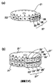
勿論、磁気ドラム21に円形内周面を形成し、ここに着磁パターンを形成し、その内側に検出器を対向配置する構成を採用することもできる。また、ドラムの着磁は、図2(b)に示すように、ドラム軸線方向の上下に2枚の磁気ドラム21’、21”を配置し、これらの着磁パターンをN、S極を逆とし、各磁気ドラムに対応して、それぞれ磁気検出素子23’〜26’からなる検出器27’、および磁気検出器23”〜26”からなる検出器27”を配置し、これらの検出器出力に基づき差動で検出してもよい。
【0020】
また、回転位置を検出するために、図3(a)に示すような回転ディスク31を採用し、前記着磁面を、当該回転ディスク31の上側あるいは下側の所定の幅の円環状端面32、33の何れかとすることができる。例えば、4ビット構成のM系列パターンによる着磁パターンを形成する場合には、当該着磁パターンのN、S極の形成ピッチと同一角度ピッチで円弧状に配列した4連の磁気検出素子34〜37からなる検出器38を着磁パターンに対向配置すればよい。
【0021】
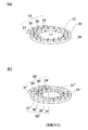
この場合においても、着磁パターンは、円環状部材である回転ディスク31の上面あるいは下面に、リングマグネットを貼りつけてもよいし、磁性材からなる円環状部材の上面あるいは下面に、直接に着磁してもよい。あるいは、小さな磁石片を上面あるいは下面に貼りつける構成としてもよい。さらには、図3(b)に示すように、回転ディスクを2トラック31’、31”とし、これらに、N、S極が逆のパターンで着磁し、各パターンを、それぞれ磁気検出素子34’〜37’からなる検出器38’、および磁気検出素子34”〜37”からなる検出器38”により検出し、これらの出力に基づき、差動方式により、検出を行うようにしてもよい。
【0022】
ここで、市販のホール素子等の磁気検出素子を用いる場合には、その大きさが定まっているので、着磁パターンのピッチは、各磁気検出素子を対向配置できないような狭いピッチにすることができない。ピッチを狭くできないと、分解能も高めることができない。そこで、上記の図3に示す構成に加えて次のような構成を付加することにより、市販の磁気検出素子を用いて、高分解能のセンサを実現可能とすることが望ましい。
【0023】
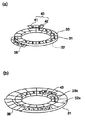
すなわち、図3(a)に示すように、円環状部材(回転ディスク)31における一方の円環状端面32が前記着磁パターンに従って着磁された着磁面(アブソリュート検出パターン面)とされる。また、図4(a)に示すように、当該円環状部材31の他方の円環状端面33は、前記着磁パターンのm倍の着磁ピッチ(m:正の整数)で、N、S極が交互に形成された第2の着磁面(インクリメンタル検出パターン面)とされる。さらに、この第2の着磁面に対向させて、2個の磁気検出素子41、42が配列された構成の第2の検出器43が配置されている。
【0024】
この代わりに、図4(b)に示すように、回転ディスク31の同一側の面に、同心状に、2つのトラックを形成し、例えば外側のトラックをアブソリュート検出パターン面(32)とし、内側のトラックをインクリメンタル検出パターン面(33)とし、それぞれのトラックに対向するように、検出器38、43を配置することもできる。勿論、外側にインクリメンタル検出パターン面を形成し、内側にアブソリュート検出パターン面を形成してもよい。
【0025】
この第2の着磁面の着磁を正弦波状に行うことにより、検出器43からは正弦波状の検出信号を得ることができる。また、磁気検出素子として、MR素子のような正弦波状の検出出力を得やすい素子を採用して、正弦波状の検出信号を得るようにしてもよい。
【0026】
検出器43の2個の検出素子41、42を、N、Sの着磁パターンピッチの半分のピッチで配列することにより、図5に示すように、双方の検出素子からは、90度位相がずれた2相の信号出力を得ることができる。
【0027】
ここで、一般的に知られている電気分割技術を用いれば、図5に示す2相の正弦波信号を多分割することが可能である。1ピッチ分の2相の正弦波信号部分を多分割することにより得られた分割出力は、1ピッチ内の絶対位置を表す信号となる。よって、検出器38で得られた各1ビット分の絶対位置間を、第2の検出器43を分割することにより得られる分割出力によって分割することにより、高分解能のアブソリュートセンサを実現できる。
【0028】
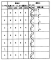
この高分解能化のステップを、図6に示してある。この図は、前記着磁パターンとして4ビットの乱数パターンを採用した例を示してあり、最も左の欄はピッチ番号(ディスクのアドレス番号)、次の欄は4ビットの検出パターン(検出器38により得られる検出出力)、その次の欄は検出器43により得られる検出信号を示し、右欄は各ピッチ番号(ディスクのアドレス番号)の位置を2n分割した状態を示してある。
【0029】
この例において、正弦波信号を4ビット分割すれば、全体の分割数は、
24×24=28=256分割
となり、10ビット分割すれば、
24×210=214=16,384分割
となる。
【0030】
ここで、この構成は、図2に示す回転ドラム方式のアブソリュートセンサにも同様に適用できる。この場合には、上記の図2の構成において、円筒状部材(磁気ドラム21)における外周面22および内周面(図示せず)のうちの一方の面を着磁パターンに従って着磁された着磁面とし、当該円筒状部材(磁気ドラム21)の他方の面を、前記着磁パターンのm倍の着磁ピッチ(m:正の整数)で、N、S極が交互に形成された第2の着磁面とし、この第2の着磁面に対向させて、2個の磁気検出素子が配列された構成の第2の検出器を配置し、前記検出器および前記第2の検出器の検出出力に基づき、前記円筒状部材あるいは前記検出器の側の絶対位置を検出すればよい。
【0031】
次に、M系列パターンを着磁パターンとして採用している光学式エンコーダの場合には、受光素子をエンコーダ専用に製作することが一般的に行われており、エンコーダを小型するためにも、複数の受光素子を隣り合うように配列した構成の検出器を用いることが望ましく、従って、光学的な検出パターンとしてM系列パターンを採用することは装置小型化にとっても望ましい。
【0032】
しかしながら、本発明の対象である磁気式のアブソリュートセンサの場合には、着磁パターンの着磁ピッチをあまり小さくできず、また、センサ専用の磁気検出素子を新たに製作するには多額の費用が掛かる。よって、市販の磁気検出素子を利用することが有利である。この場合、着磁ピッチに比べて磁気検出素子の寸法が大きい場合には、着磁ピッチに対応した状態で複数個の磁気検出素子を隣合わせで配列できない。
【0033】
そこで、本発明のアブソリュートセンサにおいては、n個の磁気検出素子を隣接配置せずに、離散した状態に配置する構成を採用している。
【0034】
すなわち、図7に示すように、着磁パターンが形成された着磁面70を検出する検出器78は、前記n個の磁気検出素子74〜77以外に、更にk個(k:正の整数)の磁気検出素子79を備えており、前記n個の磁気検出素子74〜77は、相互に隣接しない位置において前記着磁面70に対向配置され、前記k個の磁気検出素子79は、相互に異なる位置であって、且つ、前記n個の磁気検出素子74〜77のそれぞれとも異なる位置において前記着磁面70に対向配置され、これら(n+k)個の磁気検出素子74〜77、79の検出出力に基づき、着磁部材71あるいは検出器78の側の絶対位置を検出する構成を採用している。
【0035】
図7の着磁パターンは、図1に示す4ビットのM系列パターンを円周上に展開したものである。この図において、a〜dの位置(ディスクアドレスが1〜4)に磁気検出素子を配置した場合には検出パターンは図1に示す場合と同一である。しかるに、本発明では、16分割されたディスクアドレス0〜15における1、5、9、13のアドレス位置に4個の磁気検出素子74〜77を対向配置し、第2の検出器に含まれる磁気検出素子79を4のアドレス位置に対向配置してある。
【0036】
この場合には、着磁部材(回転ディスク)71の回転に伴って、図8に示すように、4個の磁気検出素子74〜77から得られる4ビットの検出パターンが変化する。しかし、この検出パターンにおいては、回転ディスクのアドレス3、11に磁気検出素子74が対向した回転位置において得られる検出パターンが同一となってしまう。同様に、回転ディスクのアドレス7、15が磁気検出素子74に位置した回転位置においも検出パターンが同一となってしまう。このことは、4ビットの検出パターンの10進換算値から明らかである。この結果、絶対位置検出が不可能になってしまう。
【0037】
しかるに、本発明では、第2の検出器を備え、そこに含まれている磁気検出素子79による検出パターンも考慮している。図示の例では合計で5ビットの検出パターンが各回転位置毎に得られ、これらの5ビットの検出パターンは、その10進換算値から明らかなように相互に異なっている。よって、絶対位置検出が可能になる。
【0038】
このように、本発明では、磁気検出素子の離散配置を採用可能としているので、着磁パターンの着磁ピッチの広狭等に関係なく、市販の磁気検出素子を用いることが可能になる。よって、磁気式のアブソリュートセンサを廉価にしかも簡単に実現できる。
【0039】
また、図7に示すように、磁気検出素子を1個あるいは2個以上追加することにより、磁気検出素子を離散配置しても、例えば、一般的に使用されているM系列パターンを着磁パターンとして利用して絶対位置を検出できる。
【0040】
次に、本発明における図2、図3を参照して説明した構成は、磁気誘導式のアブソリュートセンサにも同様に適用できる。すなわち、本発明は、図9を参照して説明すると、ステータ91と、ロータ92と、前記ステータ91に配置された一次側励磁コイル93および二次側誘導コイル94とを有し、前記ロータ92は、回転位置に応じて、前記ステータ91の前記一次側励磁コイル93および二次側誘導コイル94間の磁気結合を変化させるように構成されている磁気誘導型のアブソリュートセンサ90にも適用できる。
【0041】
この場合には、前記ロータ92には、同心円上に、等角度ピッチで形成された2n個の区画部分(図において0〜15の番号が付された部分)が形成され、各区画部分は、磁束透過部分および磁束遮断部分の何れかにパターン付けされている。また、前記ステータ91には、同心円上に、n個(n:正の整数)の前記二次側誘導コイル94が配置され、各二次側誘導コイル94は相互に異なる前記区画部分に対峙するように配置されている。さらには、前記区画部分に形成された磁束透過部分および磁束遮断部分からなるパターンは、前記ロータを等角度ピッチずつ回転させた場合に、前記n個の二次側誘導コイル94が対峙するn個分の区画部分のパターンが回転毎に変化するように設定されている。
【0042】
例えば、ロータ92としては銅板を用いることができ、この場合には、磁束透過部分は銅板に形成した貫通孔101である。図9(c)に示すように、一次側コイル93に交流を流すと、そこに交流磁束が発生する。この磁束は、外周の磁性リング102と二次側コイル94の中心に位置する磁極ピン103を通る磁気回路を構成し、この結果、二次側コイル94には電圧信号が誘起される。
【0043】
ここで、二次側コイル94に銅製のロータ92を対向配置すると、一次側コイル93の磁束によって銅板には渦電流が生じ、磁路が断たれて二次側コイル94には電圧が誘起されない。これに対して、貫通孔101の部分が二次側コイル94に対峙した状態では、当該部分を通って磁気回路が形成されるので、二次側コイル94には電圧が誘起される。
【0044】
従って、貫通孔101が形成されている区画部分が図1に示す検出パターンの「1」に相当し、孔が形成されていない区画部分が検出パターンの「0」に相当する。従って、貫通孔101を、M系列パターンあるいは乱数パターンに従って形成すれば、前述した場合と同様に絶対位置を検出できる。
【0045】
ここで、磁束透過部分と磁束遮断部分からなる検出パターンは、導電材質板に形成した孔の有無により規定できるが、この孔を形成する代わりに、非磁性板の表面に、磁性材料の小片を貼りつけるようにしてもよい。また、銅板の代わりに他の導電材料を用いても良く、さらには、絶縁板の表面に磁性体を貼ってもよい。
【0046】
いずれにせよ、ロータの検出パターンは、渦電流により所定の二次側コイルの磁束を遮断し、二次側コイルでの電圧の誘起を阻止するか、あるいは、磁性材料によって二次側コイルに磁束を通して誘起電圧を発生させる構造の何れかの方法により形成すればよい。勿論、双方の構造を併用して検出パターンを形成することもできる。
【0047】
この構成の磁気誘導型のアブソリュートセンサにおいても、本発明においては、図7に示すように、第2の検出器を配置して、回転位置によって重複した検出パターンが得られることを回避する構成を採用している。
【0048】
すなわち、前記n個の二次側誘導コイル以外に、更にk個(k:正の整数)の二次側誘導コイルを備えており、前記n個の二次側誘導コイルは、相互に隣接しない位置において前記ステータの区画部分に対向配置され、前記k個の二次側誘導コイルは、相互に異なる位置であって、且つ、前記n個の二次側誘導コイルのそれぞれとも異なる位置において前記区画部分に対向配置され、これら(n+k)個の二次側誘導コイルの検出出力に基づき、前記ロータの絶対回転位置を検出する構成となっている。
【0049】
このように二次側コイルを離散配置することができると、装置を小型化できる。すなわち、図10(a)に示すように、例えば4個の二次側コイル105〜108を隣り合わせに配列した場合には、コイル外径寸法により、装置全体の外径寸法を小さくすることが制限される。これに対して、離散配置を採用可能な本発明においては、図10(b)に示すように、例えば、90度間隔で4個の二次側コイル105〜108を配置すれば、装置全体の外径寸法を、二次側コイルの外径寸法に左右されることなく、大幅に小さくできる。換言すると、装置外径寸法が同一の場合には、その分解能を高めることができる。
【0050】
ここで、上記の図9、10に関する説明においては、便宜的に、磁気検出部を二次側コイルとして説明してきたが、実際には、磁気検出部は磁極ピンと、その外周に巻いたコイル巻線とで成り立っている。従って、上記の説明は、図10(c)に示すような磁極ピン151の外周に同心状にコイル巻線152が巻かれた構成の磁気検出部を想定している。
【0051】
しかし、磁気検出部としては、図10(d)に示すように、磁極ピン161がL形に折れ曲がり、その下側部分にコイル巻線162が巻かれた構成も考えられる。この場合には、検出パターンに対峙させる部分は、磁極ピン161の端面部分161aである。よって、この場合には、図10(e)に示すように配置することにより、検出装置全体の小型化を達成できる。なお、磁極ピンは、珪素鋼板のような磁性材料をプレス成形することにより製造できる。
【0052】
次に、本発明の上記の各構成は、リニアセンサにも同様に適用できる。すなわち、図4に示すような分解能を高めるための構成を採用する場合には、本発明の着磁部材は平行に延びる第1および第2の平面を備えており、前記第1の平面は前記着磁パターンにより着磁された前記着磁面であり、前記第2の平面は、前記着磁パターンのm倍の着磁ピッチ(m:正の整数)で、N、S極が交互に形成された第2の着磁面とされ、この第2の着磁面に対向させて、2個の磁気検出素子が配列された構成の第2の検出器が配置されており、前記検出器および前記第2の検出器の検出出力に基づき、前記着磁部材あるいは前記検出器の側の絶対位置を検出する構成とされる。
【0053】
次に、上記構成の磁気式のアブソリュートセンサにおける磁気検出素子の離散配置は、光学式のアブソリュートセンサに対しても同様に適用できる。
【0054】
すなわち、本発明は、円周方向あるいは直線状に所定の光透過パターンあるいは光反射パターンが形成されたパターン形成面を備えたパターン形成部材と、前記パターン形成面に対向配置された複数の光検出素子を備えた検出器とを有し、これらパターン形成部材および検出器を相対移動させることにより得られる前記検出器の検出出力に基づき、前記パターン形成部材あるいは検出器の側の絶対位置を検出する光学式のアブソリュートセンサにおいて、次の構成を採用している。
【0055】
すなわち、前記光透過パターンあるいは光反射パターンは、等ピッチで形成された2n個(n:正の整数)の各パターン形成区画部分に、所定の配列パターンで、光透過および光遮断部分、あるいは光反射および光吸収部分が形成されている。
【0056】
また、前記検出器はn個の光検出素子を備え、各光検出素子は相互に異なる前記パターン形成区画部分に対峙するように配置されている。
【0057】
さらに、前記光透過あるいは光反射パターンは、前記パターン形成部材および前記検出器をパターン形成ピッチずつ相対移動させた場合に、前記n個の光検出素子が対峙するn個分のパターン形成区画部分の光透過あるいは光反射パターン配列が相対移動毎に変化するように設定されている。
【0058】
さらには、前記検出器は、前記n個の光検出素子以外に、更にk個(k:正の整数)の光検出素子を備えている。
【0059】
これに加えて、前記n個の光検出素子は、相互に隣接しない位置において前記パターン形成面に対向配置されている。
【0060】
また、前記k個の光検出素子は、相互に異なる位置であって、且つ、前記n個の光検出素子のそれぞれとも異なる位置において前記パターン形成面に対向配置されている。
【0061】
そして、これら(n+k)個の光検出素子の検出出力に基づき、前記パターン形成部材あるいは前記検出器の側の絶対位置を検出するようになっている。
【0062】
この場合、前記光透過あるいは光反射パターンとしては、光透過部分および光遮断部分、あるいは光反射部分および光吸収部分が、nビットのM系列パターンに従って配列されたものを採用できる。本発明によれば、M系列パターンを採用している場合でも、受光素子の離散配置構成を採用できるので、装置レイアウトが容易になる等の利点がある。
【0063】
【発明の効果】
以上説明したように、本発明の磁気式のアブソリュートセンサにおいては、M系列パターン、乱数パターン等に従った着磁パターンを複数の磁気検出素子で検出し、それらの検出パターンに基づき回転部材あるいはスライド部材の回転位置あるいはスライド位置の絶対位置を検出している。従って、従来の磁気式のアブソリュートセンサに比べて、装置構成を小型化でき、また、廉価に製造することが可能になる。
【0064】
また、本発明においては、N、Sが交互に着磁された第2の着磁パターンも検出することにより、M系列パターン等に従って形成された着磁パターンにより得られた各絶対位置内を、第2の着磁パターンにより得られた検出信号に基づき多分割化できるようにしているので、高分解能のアブソリュートセンサを実現できる。
【0065】
さらには、本発明においては、M系列パターン等を着磁パターンとして採用した場合に、複数の磁気検出素子の離散配置を可能としているので、市販の磁気検出素子等をそのまま用いることが可能になり、センサを廉価に製造できる。
【0066】
一方、本発明による光学式のアブソリュートセンサにおいては、M系列パターン等を検出パターンとして採用した場合に、複数の受光素子の離散配置を可能としているので、装置レイアウトが容易になる等の利点が得られる。
【図面の簡単な説明】
【図1】 4ビットのM系列パターンを利用した光学式のアブソリュートセンサの検出原理を説明するための説明図である。
【図2】 磁気ドラム式のアブソリュートセンサを示すための説明図である。
【図3】 回転ディスク式のアブソリュートセンサを示すための説明図である。
【図4】 高分解能の回転ディスク式のアブソリュートセンサを示すための説明図である。
【図5】 図4における第2の検出器から得られる検出信号の例を示す信号波形図である。
【図6】 図4のアブソリュートセンサによる絶対位置の検出原理を示すための説明図である。
【図7】 本発明を適用した検出素子を離散配置可能な磁気式のアブソリュートセンサを示すための説明図である。
【図8】 図7のセンサの検出原理を説明するための説明図である。
【図9】 磁気誘導式のアブソリュートセンサを示すための説明図である。
【図10】 図9のアブソリュートセンサにおける二次側検出コイルの離散配置による装置小型化の効果を示すための説明図である。
【図11】 従来の磁気式のアブソリュートセンサの例を示す説明図である。
【図12】 従来の磁気式のアブソリュートセンサの別の例を示す説明図である。
【符号の説明】
21 円筒状部材
22 外周面
23〜26 磁気検出素子
27 検出器
31 円環状部材
32 上面
33 下面
34〜37 磁気検出素子
38 検出器
41、42 磁気検出素子
43 第2の検出器
70 着磁面
71 着磁部材
74〜77 磁気検出素子
79 磁気検出素子
90 磁気誘導式のセンサ
91 ステータ
92 ロータ
93 一次側コイル
94 二次側コイル
101 貫通孔(磁束透過部分)
105〜108 二次側コイル[0001]
BACKGROUND OF THE INVENTION
The present invention relates to an absolute sensor capable of detecting the rotational position of a rotating member and the moving position of a linearly moving member as absolute positions, and more particularly to a small and high-resolution absolute sensor.
[0002]
[Prior art]
As the absolute sensor capable of detecting the rotation position and slide position of the member as absolute information, an optical sensor is mainly used. The detection principle of the optical absolute sensor is that a binary pattern (slit or reflecting surface) is formed on a track corresponding to a detection bit, an arrangement pattern of light transmitting portions and light shielding portions according to an M series pattern, or light. A method for forming an array pattern of reflection portions and light absorption portions is known. In any case, the amount of light transmitted or reflected through the pattern is output as an electrical signal corresponding to the amount of received light from the light receiving element disposed opposite to the track, and the rotational position or slide position is determined based on the detection signal. It comes to detect.
[0003]
Magnetic type sensors are also known as absolute sensors other than the optical type. This magnetic type absolute sensor mainly includes a magnetic pattern type and a resolver type.
[0004]
As shown in FIG. 11, the magnetic pattern type absolute sensor has a configuration in which a magnetic pattern 112 is formed on the outer peripheral surface of a
[0005]
In contrast, in the resolver type absolute sensor, as shown in FIG. 12, when the
[0006]
[Problems to be solved by the invention]
A magnetic absolute sensor is generally more expensive than an optical absolute sensor and has disadvantages such as a large size.
[0007]
For example, in the former magnetic drum type absolute sensor, since it is necessary to form a large number of magnetic patterns in the axial direction on the outer peripheral surface of the magnetic drum, the surface of a thin rotating plate as in the case of the optical type In comparison with the case where a large number of optical patterns are formed concentrically in the radial direction, the dimension (thickness) in the axial direction increases, and as a result, the inertia of the rotating drum also increases.
[0008]
In the latter resolver type absolute sensor, it is necessary to place a molded core on the rotor and stator as the magnetic material, so that the mold cost is required, the winding cost is high, and the phase difference Since a peripheral electronic circuit for converting the angle into an angle is necessary, there is a disadvantage that the cost is higher than that of an optical type.
[0009]
An object of the present invention is to propose a magnetic absolute sensor that can be configured in a small size and at low cost in view of the above points.
[0010]
Another object of the present invention is to propose a magnetic absolute encoder that is small and inexpensive and has high resolution.
[0011]
Still another object of the present invention is to propose an optical absolute sensor that is inexpensive and has high resolution.
[0012]
[Means for Solving the Problems]
In order to solve the above problems, in the present invention, a random number pattern, an M-sequence pattern, and a magnetic pattern defined by other methods are formed on one track, and this is detected by a plurality of magnetic detections arranged corresponding to the track. A configuration is adopted in which detection is performed as absolute position information by a detector having an element.
[0013]
The detection principle according to the present invention will be described by taking an M-sequence pattern used in an optical absolute sensor as an example. First, FIG. 1A shows an M-sequence pattern. Since the M-sequence pattern has a 4-bit configuration, there are 24 resolutions. In the case of an optical rotary encoder, one rotation of the rotating disk is divided into 16 parts, and an M-sequence pattern having “0” as a light shielding part and “1” as a transmission part is formed on the detection track. A detector composed of four light receiving elements a to d is disposed opposite to the detection track. Assuming that the addresses of the M-sequence pattern formed on the track of the rotating disk are 0 to 15 as shown in the figure, when the disk moves with respect to the detector, the outputs of the light receiving elements a to d are shown as they rotate. Changes as shown.
[0014]
As can be seen from FIG. 1B, when the relationship between the disk position and the detector output is viewed, the output is not the same at each of the 16 divided rotation positions. Therefore, the absolute rotational position can be detected. Even with a method other than the M-sequence pattern, it is possible to obtain an optical binary pattern from which a different output is obtained for each rotational position.
[0015]
The magnetic absolute sensor of the present invention replaces such an optical binary pattern with a magnetic binary pattern, and realizes a small and inexpensive magnetic absolute sensor using the magnetic binary pattern. It is doing.
[0016]
That is, the present invention is a detection comprising a magnetized member having a magnetized surface magnetized in a predetermined pattern in the circumferential direction or the plane direction, and a plurality of magnetic detecting elements arranged opposite to the magnetized surface. In the absolute sensor for detecting the absolute position on the magnetized member or detector side based on the detection output of the detector obtained by relatively moving the magnetized member and the detector, The magnetized pattern was formed at an equal pitch 2 n N (N: positive integer) magnetized sections are magnetized with N and S poles in a predetermined arrangement pattern, and the detector includes n magnetic detection elements, and each magnetic detection The elements are arranged so as to oppose the different magnetized partition portions, and the magnetized pattern has the n pieces when the magnetized member and the detector are moved relative to each other by the magnetized pitch. The magnetizing array pattern of the n magnetizing sections facing the magnetic detecting elements is set so as to change every relative movement.
[0017]
Here, in order to detect the rotational position, a
[0018]
For example, when a magnetized pattern is formed by a 4-bit M-series pattern, quadruple magnetic detection elements arranged in an arc shape at the same angular pitch as the N and S pole formation pitch of the magnetized pattern What is necessary is just to arrange | position the
[0019]
Of course, it is also possible to adopt a configuration in which a circular inner peripheral surface is formed on the
[0020]
Further, in order to detect the rotational position, a
[0021]
Also in this case, the magnetizing pattern may be attached to the upper surface or the lower surface of the
[0022]
Here, when using a magnetic detection element such as a commercially available Hall element, the size of the magnetic detection element is fixed. Therefore, the pitch of the magnetized pattern should be narrow so that the magnetic detection elements cannot be opposed to each other. Can not. If the pitch cannot be narrowed, the resolution cannot be increased. Therefore, it is desirable to realize a high-resolution sensor using a commercially available magnetic detection element by adding the following configuration in addition to the configuration shown in FIG.
[0023]
That is, as shown in FIG. 3A, one
[0024]
Instead, as shown in FIG. 4 (b), two tracks are formed concentrically on the same surface of the
[0025]
By performing magnetization of the second magnetized surface in a sine wave shape, a sine wave detection signal can be obtained from the
[0026]
By arranging the two
[0027]
Here, if a generally known electric division technique is used, the two-phase sine wave signal shown in FIG. 5 can be divided into multiple portions. A divided output obtained by dividing the two-phase sine wave signal portion for one pitch into multiple signals becomes a signal representing an absolute position within one pitch. Therefore, a high resolution absolute sensor can be realized by dividing the absolute position of each 1 bit obtained by the
[0028]
This step of increasing the resolution is shown in FIG. This figure shows an example in which a 4-bit random number pattern is adopted as the magnetization pattern. The leftmost column is a pitch number (disk address number), and the next column is a 4-bit detection pattern (detector 38). The next column shows the detection signal obtained by the
[0029]
In this example, if the sine wave signal is divided into 4 bits, the total number of divisions is
2 Four × 2 Four = 2 8 = 256 divisions
If 10 bits are divided,
2 Four × 2 Ten = 2 14 = 16,384 division
It becomes.
[0030]
Here, this configuration can be similarly applied to the rotary drum type absolute sensor shown in FIG. In this case, in the configuration of FIG. 2 described above, one of the outer
[0031]
Next, in the case of an optical encoder that employs an M-sequence pattern as a magnetized pattern, it is common practice to manufacture a light receiving element exclusively for the encoder. It is desirable to use a detector having a configuration in which the light receiving elements are arranged adjacent to each other. Therefore, it is desirable to reduce the size of the apparatus by adopting an M series pattern as an optical detection pattern.
[0032]
However, in the case of the magnetic type absolute sensor which is the subject of the present invention, the magnetization pitch of the magnetization pattern cannot be made very small, and it is expensive to newly manufacture a magnetic detection element dedicated to the sensor. It takes. Therefore, it is advantageous to use a commercially available magnetic detection element. In this case, when the size of the magnetic detection element is larger than the magnetization pitch, a plurality of magnetic detection elements cannot be arranged side by side in a state corresponding to the magnetization pitch.
[0033]
Therefore, the absolute sensor of the present invention employs a configuration in which n magnetic detection elements are arranged in a discrete state without being arranged adjacent to each other.
[0034]
That is, as shown in FIG. 7, in addition to the n
[0035]
The magnetized pattern in FIG. 7 is obtained by developing the 4-bit M-sequence pattern shown in FIG. 1 on the circumference. In this figure, when the magnetic detection elements are arranged at positions a to d (disk addresses 1 to 4), the detection pattern is the same as that shown in FIG. However, in the present invention, the four
[0036]
In this case, as the magnetized member (rotating disk) 71 rotates, the 4-bit detection pattern obtained from the four
[0037]
However, in the present invention, the second detector is provided, and a detection pattern by the
[0038]
As described above, in the present invention, since the discrete arrangement of the magnetic detection elements can be adopted, it is possible to use a commercially available magnetic detection element regardless of whether the magnetization pitch of the magnetization pattern is wide or narrow. Therefore, a magnetic absolute sensor can be easily realized at low cost.
[0039]
Further, as shown in FIG. 7, even if the magnetic detection elements are discretely arranged by adding one or more magnetic detection elements, for example, a generally used M-sequence pattern is a magnetization pattern. Can be used to detect the absolute position.
[0040]
Next, the configuration described with reference to FIGS. 2 and 3 in the present invention can be similarly applied to a magnetic induction type absolute sensor. That is, the present invention will be described with reference to FIG. 9, which includes a
[0041]
In this case, the
[0042]
For example, a copper plate can be used as the
[0043]
Here, when the
[0044]
Accordingly, the section where the through hole 101 is formed corresponds to “1” of the detection pattern shown in FIG. 1, and the section where no hole is formed corresponds to “0” of the detection pattern. Therefore, if the through hole 101 is formed according to the M series pattern or the random number pattern, the absolute position can be detected as in the case described above.
[0045]
Here, the detection pattern consisting of the magnetic flux transmission part and the magnetic flux interruption part can be defined by the presence or absence of a hole formed in the conductive material plate, but instead of forming this hole, a small piece of magnetic material is applied to the surface of the nonmagnetic plate. You may make it stick. Moreover, you may use another electrically conductive material instead of a copper plate, and also you may affix a magnetic body on the surface of an insulating plate.
[0046]
In any case, the detection pattern of the rotor blocks the magnetic flux of a predetermined secondary coil by eddy current and prevents induction of voltage in the secondary coil, or the magnetic flux is applied to the secondary coil by a magnetic material. It may be formed by any method of a structure for generating an induced voltage through the electrode. Of course, a detection pattern can be formed by using both structures together.
[0047]
Also in the magnetic induction type absolute sensor having this configuration, in the present invention, as shown in FIG. 7, the second detector is arranged so as to avoid an overlapped detection pattern depending on the rotational position. Adopted.
[0048]
That is, in addition to the n secondary side induction coils, k (k: positive integer) secondary side induction coils are provided, and the n secondary side induction coils are not adjacent to each other. The k secondary side induction coils are arranged opposite to the stator partition portion at a position, and the k secondary side induction coils are at positions different from each other and at positions different from each of the n secondary side induction coils. It is arranged so as to face the part and is configured to detect the absolute rotational position of the rotor based on the detection outputs of these (n + k) secondary induction coils.
[0049]
If the secondary coils can be discretely arranged in this way, the apparatus can be miniaturized. That is, as shown in FIG. 10 (a), for example, when four
[0050]
9 and 10, the magnetic detection unit has been described as a secondary coil for the sake of convenience. However, in actuality, the magnetic detection unit has a magnetic pole pin and a coil wound around the outer periphery thereof. It consists of lines. Therefore, the above description assumes a magnetic detection unit having a configuration in which the coil winding 152 is concentrically wound around the outer periphery of the
[0051]
However, as the magnetic detection unit, as shown in FIG. 10 (d), a configuration in which the
[0052]
Next, each of the above-described configurations of the present invention can be similarly applied to a linear sensor. That is, when the configuration for increasing the resolution as shown in FIG. 4 is adopted, the magnetized member of the present invention includes first and second planes extending in parallel, and the first plane is The magnetized surface is magnetized by a magnetized pattern, and the second plane is alternately formed with N and S poles at a magnetizing pitch (m: positive integer) that is m times the magnetized pattern. A second detector having a configuration in which two magnetic detection elements are arranged is arranged opposite to the second magnetized surface, and the detector and Based on the detection output of the second detector, the absolute position of the magnetized member or the detector is detected.
[0053]
Next, the discrete arrangement of the magnetic detection elements in the magnetic absolute sensor having the above configuration can be similarly applied to the optical absolute sensor.
[0054]
That is, the present invention relates to a pattern forming member having a pattern forming surface on which a predetermined light transmission pattern or light reflecting pattern is formed in a circumferential direction or a straight line, and a plurality of light detection members arranged to face the pattern forming surface. And detecting the absolute position of the pattern forming member or the detector side based on the detection output of the detector obtained by relatively moving the pattern forming member and the detector. The following configuration is adopted in the optical absolute sensor.
[0055]
That is, the light transmission pattern or the light reflection pattern is formed at an equal pitch. n Light transmitting and light blocking portions or light reflecting and light absorbing portions are formed in a predetermined arrangement pattern in each (n: positive integer) pattern forming section.
[0056]
The detector includes n photodetecting elements, and the photodetecting elements are arranged so as to face different pattern forming sections.
[0057]
Further, the light transmission or light reflection pattern is obtained by changing the pattern forming member and the detector relative to each other by a pattern formation pitch by n pattern forming section portions opposed to the n light detecting elements. The light transmission or light reflection pattern array is set to change with each relative movement.
[0058]
Further, the detector further includes k (k: positive integer) light detection elements in addition to the n light detection elements.
[0059]
In addition, the n photodetecting elements are arranged to face the pattern forming surface at positions that are not adjacent to each other.
[0060]
The k photodetecting elements are disposed opposite to the pattern formation surface at positions different from each other and at positions different from the n photodetecting elements.
[0061]
Based on the detection outputs of these (n + k) light detection elements, the absolute position on the pattern forming member or the detector side is detected.
[0062]
In this case, as the light transmission or light reflection pattern, a pattern in which a light transmission portion and a light blocking portion, or a light reflection portion and a light absorption portion are arranged according to an n-bit M-sequence pattern can be employed. According to the present invention, even when the M-sequence pattern is adopted, the discrete arrangement configuration of the light receiving elements can be adopted, so that there is an advantage that the device layout becomes easy.
[0063]
【The invention's effect】
As described above, in the magnetic absolute sensor of the present invention, a magnetized pattern according to an M-sequence pattern, a random number pattern, or the like is detected by a plurality of magnetic detection elements, and a rotating member or a slide is based on these detection patterns. The absolute position of the rotation position or slide position of the member is detected. Therefore, compared with the conventional magnetic absolute sensor, the apparatus configuration can be reduced in size and can be manufactured at low cost.
[0064]
Further, in the present invention, by detecting the second magnetization pattern in which N and S are alternately magnetized, within each absolute position obtained by the magnetization pattern formed according to the M series pattern or the like, Since the multi-division can be performed based on the detection signal obtained by the second magnetization pattern, a high-resolution absolute sensor can be realized.
[0065]
Furthermore, in the present invention, when an M series pattern or the like is adopted as a magnetized pattern, a plurality of magnetic detection elements can be arranged in a discrete manner, so that a commercially available magnetic detection element or the like can be used as it is. The sensor can be manufactured at low cost.
[0066]
On the other hand, in the optical absolute sensor according to the present invention, when an M-sequence pattern or the like is adopted as a detection pattern, it is possible to dispose a plurality of light receiving elements in a discrete manner. It is done.
[Brief description of the drawings]
FIG. 1 is an explanatory diagram for explaining the detection principle of an optical absolute sensor using a 4-bit M-sequence pattern.
FIG. 2 is an explanatory diagram showing a magnetic drum type absolute sensor;
FIG. 3 is an explanatory diagram showing a rotating disk type absolute sensor.
FIG. 4 is an explanatory diagram for showing a high-resolution rotary disk type absolute sensor.
5 is a signal waveform diagram showing an example of a detection signal obtained from the second detector in FIG. 4. FIG.
6 is an explanatory diagram for illustrating the principle of absolute position detection by the absolute sensor of FIG. 4; FIG.
FIG. 7 is an explanatory diagram showing a magnetic absolute sensor in which detection elements to which the present invention is applied can be discretely arranged.
8 is an explanatory diagram for explaining a detection principle of the sensor of FIG. 7;
FIG. 9 is an explanatory diagram showing a magnetic induction type absolute sensor.
10 is an explanatory diagram for illustrating the effect of downsizing the apparatus by discrete arrangement of secondary side detection coils in the absolute sensor of FIG. 9; FIG.
FIG. 11 is an explanatory view showing an example of a conventional magnetic absolute sensor.
FIG. 12 is an explanatory view showing another example of a conventional magnetic absolute sensor.
[Explanation of symbols]
21 Cylindrical member
22 Outer surface
23-26 Magnetic detection element
27 Detector
31 Toroidal member
32 Top surface
33 Bottom
34-37 Magnetic detection element
38 Detector
41, 42 Magnetic detection element
43 Second detector
70 Magnetized surface
71 Magnetized member
74-77 Magnetic detection element
79 Magnetic detection element
90 Magnetic induction sensor
91 Stator
92 Rotor
93 Primary coil
94 Secondary coil
101 Through hole (Magnetic flux transmission part)
105-108 Secondary coil
Claims (10)
前記着磁パターンは、等ピッチで形成された2n個(n:正の整数)の各着磁区画部分に、所定の配列パターンでNおよびS極が着磁されたものであり、
前記検出器はn個の磁気検出素子を備え、各磁気検出素子は相互に異なる前記着磁区画部分に対峙するように配置されており、
前記着磁パターンは、前記着磁部材および前記検出器を着磁ピッチずつ相対移動させた場合に、連続するn個分の着磁区画部分の着磁配列パターンに着目した場合に、この着磁配列パターンが相対移動毎に異なるパターンに変化し、前記n個の磁気検出素子が対峙している前記n個分の着磁区画部分の着磁配列パターンが相対移動毎に変化するように設定されており、
前記検出器は、前記n個の磁気検出素子以外に、更にk個(k:正の整数)の磁気検出素子を備えており、
前記n個の磁気検出素子は、相互に隣接しない位置において前記着磁面に対向配置され、
前記k個の磁気検出素子は、相互に異なる位置であって、且つ、前記n個の磁気検出素子のそれぞれとも異なる位置において前記着磁面に対向配置され、
これら(n+k)個の磁気検出素子の検出出力に基づき、前記着磁部材あるいは前記検出器の側の絶対位置を検出することを特徴とするアブソリュートセンサ。A magnetized member having a magnetized surface magnetized in a predetermined pattern in a circumferential direction or a plane direction, and a detector having a plurality of magnetic detecting elements arranged to face the magnetized surface; Based on the detection output of the detector obtained by relative movement of the magnetized member and detector in the direction of the magnetized pattern of the magnetized surface, the absolute position on the magnetized member or detector side is detected. In absolute sensor,
The magnetization pattern is obtained by magnetizing N and S poles in a predetermined arrangement pattern on each of 2 n (n: positive integer) magnetization partition portions formed at an equal pitch,
The detector includes n magnetic detection elements, and each magnetic detection element is disposed so as to face the different magnetized partition portions.
The magnetized pattern is obtained when the magnetized member and the detector are moved relative to each other by the magnetized pitch and attention is paid to the magnetized array pattern of n consecutive magnetized partition portions. The arrangement pattern changes to a different pattern for each relative movement, and the magnetization arrangement pattern of the n magnetized partition portions opposed to the n magnetic detection elements is set to change for each relative movement. And
In addition to the n magnetic detection elements, the detector further includes k (k: positive integer) magnetic detection elements,
The n magnetic detection elements are arranged to face the magnetized surface at positions not adjacent to each other,
The k magnetic detection elements are arranged opposite to the magnetized surface at positions different from each other and at positions different from the n magnetic detection elements,
An absolute sensor that detects an absolute position of the magnetized member or the detector side based on detection outputs of the (n + k) magnetic detection elements.
前記着磁面は円形外周面あるいは円形内周面であることを特徴とするアブソリュートセンサ。In claim 1,
The absolute sensor according to claim 1, wherein the magnetized surface is a circular outer peripheral surface or a circular inner peripheral surface.
前記着磁面は所定の幅の円環状端面であることを特徴とするアブソリュートセンサ。In claim 1,
The absolute sensor according to claim 1, wherein the magnetized surface is an annular end surface having a predetermined width.
円環状部材における一方の円環状端面は前記着磁パターンが形成された着磁面であり、
当該円環状部材の他方の円環状端面は、前記着磁パターンのm倍の着磁ピッチ(m:正の整数)で、N、S極が交互に形成された第2の着磁面とされ、
この第2の着磁面に対向させて、2個の磁気検出素子が配列された構成の第2の検出器が配置されており、
前記検出器および前記第2の検出器の検出出力に基づき、前記円環状部材あるいは前記検出器の側の絶対位置を検出することを特徴とするアブソリュートセンサ。In claim 3,
One annular end surface of the annular member is a magnetized surface on which the magnetized pattern is formed,
The other annular end surface of the annular member is a second magnetized surface in which N and S poles are alternately formed at a magnetization pitch (m: positive integer) that is m times the magnetization pattern. ,
A second detector having a configuration in which two magnetic detection elements are arranged is arranged opposite to the second magnetized surface,
An absolute sensor that detects an absolute position of the annular member or the detector side based on detection outputs of the detector and the second detector.
円筒状部材における外周面および内周面のうちの一方の面は前記着磁パターンが形成された着磁面であり、
当該円筒状部材の他方の面は、前記着磁パターンのm倍の着磁ピッチ(m:正の整数)で、N、S極が交互に形成された第2の着磁面とされ、
この第2の着磁面に対向させて、2個の磁気検出素子が配列された構成の第2の検出器が配置されており、
前記検出器および前記第2の検出器の検出出力に基づき、前記円環状部材あるいは前記検出器の側の絶対位置を検出することを特徴とするアブソリュートセンサ。In claim 2,
One of the outer peripheral surface and the inner peripheral surface of the cylindrical member is a magnetized surface on which the magnetized pattern is formed,
The other surface of the cylindrical member is a second magnetization surface in which N and S poles are alternately formed at a magnetization pitch (m: positive integer) that is m times the magnetization pattern.
A second detector having a configuration in which two magnetic detection elements are arranged is arranged opposite to the second magnetized surface,
An absolute sensor that detects an absolute position of the annular member or the detector side based on detection outputs of the detector and the second detector.
複数個の磁石片を部材表面に貼り付けることにより前記着磁パターンが形成されていることを特徴とするアブソリュートセンサ。In any one of claims 1 to 5,
An absolute sensor, wherein the magnetized pattern is formed by attaching a plurality of magnet pieces to a member surface.
前記ロータには、同心円上に、等角度ピッチで形成された2n個の区画部分が形成され、各区画部分は、磁束透過部分および磁束遮断部分の何れかとされ、
前記ステータには、同心円上に、n個(n:正の整数)の前記二次側誘導コイルが配置され、各二次側誘導コイルは相互に異なる前記区画部分に対峙するように配置されており、
前記区画部分に形成された磁束透過部分および磁束遮断部分の配列パターンは、前記ロータを等角度ピッチずつ回転させた場合に、連続するn個分の二次側誘導コイルの配列パターンに着目した場合に、この配列パターンが等角度ピッチずつ回転毎に異なるパターンに変化し、前記n個の二次側誘導コイルが対峙しているn個分の区画部分の配列パターンが等角度ピッチずつ回転毎に変化するように設定されており、
前記n個の二次側誘導コイル以外に、更にk個(k:正の整数)の二次側誘導コイルを備えており、
前記n個の二次側誘導コイルは、相互に隣接しない位置において前記ステータの区画部分に対向配置され、
前記k個の二次側誘導コイルは、相互に異なる位置であって、且つ、前記n個の二次側誘導コイルのそれぞれとも異なる位置において前記区画部分に対向配置され、
これら(n+k)個の二次側誘導コイルの検出出力に基づき、前記ロータの絶対回転位置を検出することを特徴とするアブソリュートセンサ。A stator, a rotor, and a primary-side excitation coil and a secondary-side induction coil disposed in the stator, the rotor according to a rotational position, the primary-side excitation coil and the secondary-side induction of the stator In the magnetic induction type absolute sensor configured to change the magnetic coupling between the coils,
In the rotor, 2n partition portions formed at equiangular pitches on a concentric circle are formed, and each partition portion is either a magnetic flux transmitting portion or a magnetic flux blocking portion,
In the stator, n (n: positive integer) secondary side induction coils are arranged on concentric circles, and each secondary side induction coil is arranged so as to be opposed to different partition portions. And
The arrangement pattern of the magnetic flux transmission part and the magnetic flux interruption part formed in the partition part is a case where attention is paid to the arrangement pattern of the n secondary induction coils that are continuous when the rotor is rotated at equal angular pitches. In addition, this arrangement pattern changes into a different pattern for each rotation at equal angular pitches, and the arrangement pattern of the n partition portions that the n secondary side induction coils are opposed to each other is rotated at equal angular pitches every rotation. Set to change,
In addition to the n secondary induction coils, k (k is a positive integer) secondary induction coils are provided,
The n secondary induction coils are disposed to face the partition portion of the stator at positions not adjacent to each other,
The k secondary side induction coils are arranged opposite to the partition portion at positions different from each other and at positions different from the n secondary side induction coils, respectively.
An absolute sensor that detects an absolute rotational position of the rotor based on detection outputs of the (n + k) secondary induction coils.
前記着磁部材は平行に延びる第1および第2の平面を備えており、
前記第1の平面は前記着磁パターンにより着磁された前記着磁面であり、
前記第2の平面は、前記着磁パターンのm倍の着磁ピッチ(m:正の整数)で、N、S極が交互に形成された第2の着磁面とされ、
この第2の着磁面に対向させて、2個の磁気検出素子が配列された構成の第2の検出器が配置されており、
前記検出器および前記第2の検出器の検出出力に基づき、前記着磁部材あるいは前記検出器の側の絶対位置を検出することを特徴とするアブソリュートセンサ。In claim 1,
The magnetized member includes first and second planes extending in parallel,
The first plane is the magnetized surface magnetized by the magnetized pattern;
The second plane is a second magnetization surface in which N and S poles are alternately formed at a magnetization pitch (m: positive integer) that is m times the magnetization pattern.
A second detector having a configuration in which two magnetic detection elements are arranged is arranged opposite to the second magnetized surface,
An absolute sensor for detecting an absolute position of the magnetized member or the detector side based on detection outputs of the detector and the second detector.
前記配列パターンは、等ピッチで形成された2n個(n:正の整数)の各パターン形成区画部分に、所定の配列パターンで、光透過および光遮断部分、あるいは光反射および光吸収部分が形成されており、
前記検出器はn個の光検出素子を備え、各光検出素子は相互に異なる前記パターン形成区画部分に対峙するように配置されており、
前記配列パターンは、前記パターン形成部材および前記検出器をパターン形成ピッチずつ相対移動させた場合に、前記n個の光検出素子が対峙しているn個分のパターン形成区画部分のパターン配列が相対移動毎に変化するように設定されており、
前記検出器は、前記n個の光検出素子以外に、更にk個(k:正の整数)の光検出素子を備えており、
前記n個の光検出素子は、相互に隣接しない位置において前記パターン形成面に対向配置され、
前記k個の光検出素子は、相互に異なる位置であって、且つ、前記n個の光検出素子のそれぞれとも異なる位置において前記パターン形成面に対向配置され、
これら(n+k)個の光検出素子の検出出力に基づき、前記パターン形成部材あるいは前記検出器の側の絶対位置を検出することを特徴とするアブソリュートセンサ。A pattern forming member provided with a pattern forming surface in which a light transmitting / blocking portion or a light reflecting / absorbing portion is formed in a predetermined arrangement pattern in a circumferential direction or a plane direction, and a plurality of pieces arranged opposite to the pattern forming surface A detector having a light detection element, and based on the detection output of the detector obtained by relatively moving the pattern forming member and the detector, the absolute position on the pattern forming member or detector side is determined. In the optical absolute sensor to detect,
The array pattern has 2 n (n: positive integer) pattern forming section portions formed at an equal pitch, and a predetermined array pattern having light transmission and light blocking portions or light reflection and light absorption portions. Formed,
The detector includes n photodetecting elements, and each photodetecting element is disposed so as to face the different pattern forming section portions,
In the arrangement pattern, when the pattern forming member and the detector are moved relative to each other by the pattern formation pitch, the pattern arrangement of the n pattern forming sections opposed to the n photodetecting elements is relative. Set to change with each move,
In addition to the n photodetecting elements, the detector further includes k (k: positive integer) photodetecting elements,
The n photodetecting elements are arranged to face the pattern forming surface at positions not adjacent to each other,
The k photodetecting elements are arranged opposite to the pattern forming surface at positions different from each other and at positions different from each of the n photodetecting elements,
An absolute sensor that detects an absolute position of the pattern forming member or the detector side based on detection outputs of the (n + k) light detection elements.
前記配列パターンは、光透過部分および光遮断部分、あるいは光反射部分および光吸収部分が、nビットのM系列パターンに従って配列されたものであることを特徴とするアブソリュートセンサ。In claim 9,
The absolute pattern is characterized in that the light transmitting portion and the light blocking portion, or the light reflecting portion and the light absorbing portion are arranged in accordance with an n-bit M series pattern.
Priority Applications (2)
| Application Number | Priority Date | Filing Date | Title |
|---|---|---|---|
| JP16323199A JP4290281B2 (en) | 1999-06-10 | 1999-06-10 | Absolute sensor |
| PCT/JP2000/008759 WO2002048653A1 (en) | 1999-06-10 | 2000-12-11 | Absolute sensor |
Applications Claiming Priority (2)
| Application Number | Priority Date | Filing Date | Title |
|---|---|---|---|
| JP16323199A JP4290281B2 (en) | 1999-06-10 | 1999-06-10 | Absolute sensor |
| PCT/JP2000/008759 WO2002048653A1 (en) | 1999-06-10 | 2000-12-11 | Absolute sensor |
Publications (3)
| Publication Number | Publication Date |
|---|---|
| JP2000352523A JP2000352523A (en) | 2000-12-19 |
| JP2000352523A5 JP2000352523A5 (en) | 2006-05-11 |
| JP4290281B2 true JP4290281B2 (en) | 2009-07-01 |
Family
ID=26344994
Family Applications (1)
| Application Number | Title | Priority Date | Filing Date |
|---|---|---|---|
| JP16323199A Expired - Lifetime JP4290281B2 (en) | 1999-06-10 | 1999-06-10 | Absolute sensor |
Country Status (2)
| Country | Link |
|---|---|
| JP (1) | JP4290281B2 (en) |
| WO (1) | WO2002048653A1 (en) |
Cited By (1)
| Publication number | Priority date | Publication date | Assignee | Title |
|---|---|---|---|---|
| CN110926557A (en) * | 2016-06-07 | 2020-03-27 | 意法半导体(鲁塞)公司 | Device for determining the movement of a rotating element |
Families Citing this family (8)
| Publication number | Priority date | Publication date | Assignee | Title |
|---|---|---|---|---|
| JP5077717B2 (en) * | 2010-04-12 | 2012-11-21 | 村田機械株式会社 | Magnetic pole detection system |
| JP2013015342A (en) * | 2011-06-30 | 2013-01-24 | Rhythm Watch Co Ltd | Clock device |
| JP6168762B2 (en) * | 2012-12-14 | 2017-07-26 | キヤノン株式会社 | Absolute encoder |
| CN105229424B (en) * | 2013-05-21 | 2017-05-24 | 三菱电机株式会社 | Method for self-calibrating a rotary encoder |
| JP6487246B2 (en) * | 2015-03-26 | 2019-03-20 | 三菱重工工作機械株式会社 | Electromagnetic induction position detector and position detection method using the same |
| JP2020100214A (en) * | 2018-12-20 | 2020-07-02 | 日立オートモティブシステムズ株式会社 | Steering device |
| JP7353992B2 (en) | 2020-01-14 | 2023-10-02 | 株式会社ミツトヨ | Rotary encoder |
| JP7162784B1 (en) * | 2022-03-23 | 2022-10-28 | 三菱電機株式会社 | Absolute encoder and electric motor |
Family Cites Families (2)
| Publication number | Priority date | Publication date | Assignee | Title |
|---|---|---|---|---|
| JPS63177019A (en) * | 1986-10-09 | 1988-07-21 | Alpine Electron Inc | Position sensor |
| JP2691943B2 (en) * | 1990-04-19 | 1997-12-17 | 株式会社ニコン | 1-track type absolute encoder |
-
1999
- 1999-06-10 JP JP16323199A patent/JP4290281B2/en not_active Expired - Lifetime
-
2000
- 2000-12-11 WO PCT/JP2000/008759 patent/WO2002048653A1/en unknown
Cited By (3)
| Publication number | Priority date | Publication date | Assignee | Title |
|---|---|---|---|---|
| CN110926557A (en) * | 2016-06-07 | 2020-03-27 | 意法半导体(鲁塞)公司 | Device for determining the movement of a rotating element |
| CN110926557B (en) * | 2016-06-07 | 2021-05-07 | 意法半导体(鲁塞)公司 | Device for determining the movement of a rotating element |
| US11079256B2 (en) | 2016-06-07 | 2021-08-03 | Stmicroelectronics (Rousset) Sas | Device for determining the movement of a rotary element, particularly for readings of water and/or gas meters |
Also Published As
| Publication number | Publication date |
|---|---|
| WO2002048653A1 (en) | 2002-06-20 |
| JP2000352523A (en) | 2000-12-19 |
Similar Documents
| Publication | Publication Date | Title |
|---|---|---|
| KR101597639B1 (en) | Absolute encoder device and motor | |
| JP3883035B2 (en) | Multi-turn encoder | |
| JP4052798B2 (en) | Relative position measuring instrument | |
| JP4002308B2 (en) | Inductive rotational position detector | |
| US8710829B2 (en) | Sheet coil type resolver | |
| US6163147A (en) | Position and speed sensors for a rotating shaft | |
| JP4290281B2 (en) | Absolute sensor | |
| EP0585281B1 (en) | Inductive displacement sensors | |
| US4888986A (en) | Rotational position indicator | |
| JPH11233338A (en) | Multipolar magnetic ping | |
| JP2008029070A (en) | Angle detector | |
| JP2007093420A (en) | Rotation angle sensor | |
| EP1016852B1 (en) | Apparatus for measuring the position of a movable member | |
| WO2022124415A1 (en) | Resolver | |
| FI129373B (en) | A variable reluctance position sensor | |
| CN110906958B (en) | Multi-excitation angle measuring method | |
| KR100458235B1 (en) | Angle detector | |
| JP7270903B2 (en) | flat plate encoder | |
| EP4086586A1 (en) | Position encoder | |
| JP2979692B2 (en) | Magnetic encoder | |
| JP2676878B2 (en) | Absolute encoder | |
| JP2000352501A (en) | Magnetic induction rotating position sensor | |
| JP2024502666A (en) | Non-contact position sensor with permanent magnet, measuring device, application method of non-contact position sensor | |
| SU945639A1 (en) | Angular displacement converter | |
| JPH03191820A (en) | Magnetic encoder |
Legal Events
| Date | Code | Title | Description |
|---|---|---|---|
| A521 | Written amendment |
Free format text: JAPANESE INTERMEDIATE CODE: A523 Effective date: 20060320 |
|
| A621 | Written request for application examination |
Free format text: JAPANESE INTERMEDIATE CODE: A621 Effective date: 20060320 |
|
| A977 | Report on retrieval |
Free format text: JAPANESE INTERMEDIATE CODE: A971007 Effective date: 20081024 |
|
| A131 | Notification of reasons for refusal |
Free format text: JAPANESE INTERMEDIATE CODE: A131 Effective date: 20081030 |
|
| A521 | Written amendment |
Free format text: JAPANESE INTERMEDIATE CODE: A523 Effective date: 20081202 |
|
| A131 | Notification of reasons for refusal |
Free format text: JAPANESE INTERMEDIATE CODE: A131 Effective date: 20090113 |
|
| A521 | Written amendment |
Free format text: JAPANESE INTERMEDIATE CODE: A523 Effective date: 20090310 |
|
| TRDD | Decision of grant or rejection written | ||
| A01 | Written decision to grant a patent or to grant a registration (utility model) |
Free format text: JAPANESE INTERMEDIATE CODE: A01 Effective date: 20090331 |
|
| A01 | Written decision to grant a patent or to grant a registration (utility model) |
Free format text: JAPANESE INTERMEDIATE CODE: A01 |
|
| A61 | First payment of annual fees (during grant procedure) |
Free format text: JAPANESE INTERMEDIATE CODE: A61 Effective date: 20090401 |
|
| R150 | Certificate of patent or registration of utility model |
Ref document number: 4290281 Country of ref document: JP Free format text: JAPANESE INTERMEDIATE CODE: R150 Free format text: JAPANESE INTERMEDIATE CODE: R150 |
|
| FPAY | Renewal fee payment (event date is renewal date of database) |
Free format text: PAYMENT UNTIL: 20120410 Year of fee payment: 3 |
|
| FPAY | Renewal fee payment (event date is renewal date of database) |
Free format text: PAYMENT UNTIL: 20120410 Year of fee payment: 3 |
|
| FPAY | Renewal fee payment (event date is renewal date of database) |
Free format text: PAYMENT UNTIL: 20130410 Year of fee payment: 4 |
|
| R250 | Receipt of annual fees |
Free format text: JAPANESE INTERMEDIATE CODE: R250 |
|
| FPAY | Renewal fee payment (event date is renewal date of database) |
Free format text: PAYMENT UNTIL: 20140410 Year of fee payment: 5 |
|
| R250 | Receipt of annual fees |
Free format text: JAPANESE INTERMEDIATE CODE: R250 |
|
| R250 | Receipt of annual fees |
Free format text: JAPANESE INTERMEDIATE CODE: R250 |
|
| R250 | Receipt of annual fees |
Free format text: JAPANESE INTERMEDIATE CODE: R250 |
|
| R250 | Receipt of annual fees |
Free format text: JAPANESE INTERMEDIATE CODE: R250 |
|
| R250 | Receipt of annual fees |
Free format text: JAPANESE INTERMEDIATE CODE: R250 |
|
| R250 | Receipt of annual fees |
Free format text: JAPANESE INTERMEDIATE CODE: R250 |
|
| R250 | Receipt of annual fees |
Free format text: JAPANESE INTERMEDIATE CODE: R250 |
|
| EXPY | Cancellation because of completion of term |