JP4285954B2 - Contamination control method for embedded ferroelectric device fabrication process - Google Patents
Contamination control method for embedded ferroelectric device fabrication process Download PDFInfo
- Publication number
- JP4285954B2 JP4285954B2 JP2002232065A JP2002232065A JP4285954B2 JP 4285954 B2 JP4285954 B2 JP 4285954B2 JP 2002232065 A JP2002232065 A JP 2002232065A JP 2002232065 A JP2002232065 A JP 2002232065A JP 4285954 B2 JP4285954 B2 JP 4285954B2
- Authority
- JP
- Japan
- Prior art keywords
- substrate
- ferroelectric
- edge
- layer
- sacrificial layer
- Prior art date
- Legal status (The legal status is an assumption and is not a legal conclusion. Google has not performed a legal analysis and makes no representation as to the accuracy of the status listed.)
- Expired - Fee Related
Links
- 238000000034 method Methods 0.000 title claims description 79
- 230000008569 process Effects 0.000 title claims description 64
- 238000004519 manufacturing process Methods 0.000 title description 19
- 238000011109 contamination Methods 0.000 title description 14
- 239000000758 substrate Substances 0.000 claims description 78
- 239000003990 capacitor Substances 0.000 claims description 47
- 238000005530 etching Methods 0.000 claims description 34
- 230000007717 exclusion Effects 0.000 claims description 30
- 239000000463 material Substances 0.000 claims description 26
- 238000004140 cleaning Methods 0.000 claims description 22
- 239000000356 contaminant Substances 0.000 claims description 21
- 239000004065 semiconductor Substances 0.000 claims description 16
- 239000002253 acid Substances 0.000 claims description 11
- 238000009792 diffusion process Methods 0.000 claims description 11
- 230000004888 barrier function Effects 0.000 claims description 10
- 229910052739 hydrogen Inorganic materials 0.000 claims description 6
- 229910052731 fluorine Inorganic materials 0.000 claims description 5
- 239000011737 fluorine Substances 0.000 claims description 5
- ZAMOUSCENKQFHK-UHFFFAOYSA-N Chlorine atom Chemical compound [Cl] ZAMOUSCENKQFHK-UHFFFAOYSA-N 0.000 claims description 4
- 239000000460 chlorine Substances 0.000 claims description 4
- 229910052801 chlorine Inorganic materials 0.000 claims description 4
- 238000000151 deposition Methods 0.000 claims description 2
- PXGOKWXKJXAPGV-UHFFFAOYSA-N Fluorine Chemical compound FF PXGOKWXKJXAPGV-UHFFFAOYSA-N 0.000 claims 1
- 238000000059 patterning Methods 0.000 claims 1
- 239000010410 layer Substances 0.000 description 64
- 229910052719 titanium Inorganic materials 0.000 description 11
- 229910052726 zirconium Inorganic materials 0.000 description 11
- 229910052745 lead Inorganic materials 0.000 description 9
- 229910052741 iridium Inorganic materials 0.000 description 8
- 229910052751 metal Inorganic materials 0.000 description 6
- 239000002184 metal Substances 0.000 description 6
- 229910004298 SiO 2 Inorganic materials 0.000 description 5
- 230000015572 biosynthetic process Effects 0.000 description 5
- 239000010408 film Substances 0.000 description 5
- 239000007789 gas Substances 0.000 description 5
- 239000000126 substance Substances 0.000 description 5
- YCKRFDGAMUMZLT-UHFFFAOYSA-N Fluorine atom Chemical compound [F] YCKRFDGAMUMZLT-UHFFFAOYSA-N 0.000 description 4
- 229910052581 Si3N4 Inorganic materials 0.000 description 4
- VYPSYNLAJGMNEJ-UHFFFAOYSA-N Silicium dioxide Chemical compound O=[Si]=O VYPSYNLAJGMNEJ-UHFFFAOYSA-N 0.000 description 4
- 239000000203 mixture Substances 0.000 description 4
- 238000012545 processing Methods 0.000 description 4
- HQVNEWCFYHHQES-UHFFFAOYSA-N silicon nitride Chemical compound N12[Si]34N5[Si]62N3[Si]51N64 HQVNEWCFYHHQES-UHFFFAOYSA-N 0.000 description 4
- XUIMIQQOPSSXEZ-UHFFFAOYSA-N Silicon Chemical compound [Si] XUIMIQQOPSSXEZ-UHFFFAOYSA-N 0.000 description 3
- 229910010037 TiAlN Inorganic materials 0.000 description 3
- 238000012864 cross contamination Methods 0.000 description 3
- 238000010586 diagram Methods 0.000 description 3
- 238000005516 engineering process Methods 0.000 description 3
- 150000002739 metals Chemical class 0.000 description 3
- 230000003647 oxidation Effects 0.000 description 3
- 238000007254 oxidation reaction Methods 0.000 description 3
- 229910052710 silicon Inorganic materials 0.000 description 3
- 239000010703 silicon Substances 0.000 description 3
- UFHFLCQGNIYNRP-UHFFFAOYSA-N Hydrogen Chemical compound [H][H] UFHFLCQGNIYNRP-UHFFFAOYSA-N 0.000 description 2
- 150000007513 acids Chemical class 0.000 description 2
- 230000015556 catabolic process Effects 0.000 description 2
- 239000011248 coating agent Substances 0.000 description 2
- 238000000576 coating method Methods 0.000 description 2
- 239000000470 constituent Substances 0.000 description 2
- 230000007423 decrease Effects 0.000 description 2
- 230000006870 function Effects 0.000 description 2
- 239000001257 hydrogen Substances 0.000 description 2
- 230000010354 integration Effects 0.000 description 2
- 239000011229 interlayer Substances 0.000 description 2
- 229920002120 photoresistant polymer Polymers 0.000 description 2
- 229910052697 platinum Inorganic materials 0.000 description 2
- 238000004886 process control Methods 0.000 description 2
- 230000001681 protective effect Effects 0.000 description 2
- 239000000377 silicon dioxide Substances 0.000 description 2
- 235000012239 silicon dioxide Nutrition 0.000 description 2
- WFKWXMTUELFFGS-UHFFFAOYSA-N tungsten Chemical compound [W] WFKWXMTUELFFGS-UHFFFAOYSA-N 0.000 description 2
- 229910052721 tungsten Inorganic materials 0.000 description 2
- 239000010937 tungsten Substances 0.000 description 2
- JBRZTFJDHDCESZ-UHFFFAOYSA-N AsGa Chemical compound [As]#[Ga] JBRZTFJDHDCESZ-UHFFFAOYSA-N 0.000 description 1
- IJGRMHOSHXDMSA-UHFFFAOYSA-N Atomic nitrogen Chemical compound N#N IJGRMHOSHXDMSA-UHFFFAOYSA-N 0.000 description 1
- YZCKVEUIGOORGS-OUBTZVSYSA-N Deuterium Chemical compound [2H] YZCKVEUIGOORGS-OUBTZVSYSA-N 0.000 description 1
- 229910001218 Gallium arsenide Inorganic materials 0.000 description 1
- 229910010413 TiO 2 Inorganic materials 0.000 description 1
- 230000009471 action Effects 0.000 description 1
- 238000000137 annealing Methods 0.000 description 1
- 238000005229 chemical vapour deposition Methods 0.000 description 1
- 230000000295 complement effect Effects 0.000 description 1
- 239000004020 conductor Substances 0.000 description 1
- 238000006731 degradation reaction Methods 0.000 description 1
- 230000008021 deposition Effects 0.000 description 1
- 229910052805 deuterium Inorganic materials 0.000 description 1
- 238000011161 development Methods 0.000 description 1
- 238000011982 device technology Methods 0.000 description 1
- 239000003085 diluting agent Substances 0.000 description 1
- 229910001873 dinitrogen Inorganic materials 0.000 description 1
- 238000001312 dry etching Methods 0.000 description 1
- 230000000694 effects Effects 0.000 description 1
- 239000007772 electrode material Substances 0.000 description 1
- 239000000395 magnesium oxide Substances 0.000 description 1
- CPLXHLVBOLITMK-UHFFFAOYSA-N magnesium oxide Inorganic materials [Mg]=O CPLXHLVBOLITMK-UHFFFAOYSA-N 0.000 description 1
- AXZKOIWUVFPNLO-UHFFFAOYSA-N magnesium;oxygen(2-) Chemical compound [O-2].[Mg+2] AXZKOIWUVFPNLO-UHFFFAOYSA-N 0.000 description 1
- 238000005259 measurement Methods 0.000 description 1
- 229910044991 metal oxide Inorganic materials 0.000 description 1
- 150000004706 metal oxides Chemical class 0.000 description 1
- 238000001465 metallisation Methods 0.000 description 1
- 239000005416 organic matter Substances 0.000 description 1
- TWNQGVIAIRXVLR-UHFFFAOYSA-N oxo(oxoalumanyloxy)alumane Chemical compound O=[Al]O[Al]=O TWNQGVIAIRXVLR-UHFFFAOYSA-N 0.000 description 1
- 230000003071 parasitic effect Effects 0.000 description 1
- 230000002093 peripheral effect Effects 0.000 description 1
- 238000007747 plating Methods 0.000 description 1
- 230000010287 polarization Effects 0.000 description 1
- 229910021420 polycrystalline silicon Inorganic materials 0.000 description 1
- 229920005591 polysilicon Polymers 0.000 description 1
- 230000001737 promoting effect Effects 0.000 description 1
- 230000005855 radiation Effects 0.000 description 1
- 238000011084 recovery Methods 0.000 description 1
- 230000000717 retained effect Effects 0.000 description 1
- 229910052707 ruthenium Inorganic materials 0.000 description 1
- 229910052594 sapphire Inorganic materials 0.000 description 1
- 239000010980 sapphire Substances 0.000 description 1
- 238000005389 semiconductor device fabrication Methods 0.000 description 1
- 229910021332 silicide Inorganic materials 0.000 description 1
- FVBUAEGBCNSCDD-UHFFFAOYSA-N silicide(4-) Chemical compound [Si-4] FVBUAEGBCNSCDD-UHFFFAOYSA-N 0.000 description 1
- 229910052712 strontium Inorganic materials 0.000 description 1
- 238000004381 surface treatment Methods 0.000 description 1
- 229910052715 tantalum Inorganic materials 0.000 description 1
- 239000010409 thin film Substances 0.000 description 1
Images


Classifications
-
- H—ELECTRICITY
- H01—ELECTRIC ELEMENTS
- H01L—SEMICONDUCTOR DEVICES NOT COVERED BY CLASS H10
- H01L27/00—Devices consisting of a plurality of semiconductor or other solid-state components formed in or on a common substrate
- H01L27/02—Devices consisting of a plurality of semiconductor or other solid-state components formed in or on a common substrate including semiconductor components specially adapted for rectifying, oscillating, amplifying or switching and having potential barriers; including integrated passive circuit elements having potential barriers
- H01L27/04—Devices consisting of a plurality of semiconductor or other solid-state components formed in or on a common substrate including semiconductor components specially adapted for rectifying, oscillating, amplifying or switching and having potential barriers; including integrated passive circuit elements having potential barriers the substrate being a semiconductor body
- H01L27/10—Devices consisting of a plurality of semiconductor or other solid-state components formed in or on a common substrate including semiconductor components specially adapted for rectifying, oscillating, amplifying or switching and having potential barriers; including integrated passive circuit elements having potential barriers the substrate being a semiconductor body including a plurality of individual components in a repetitive configuration
- H01L27/105—Devices consisting of a plurality of semiconductor or other solid-state components formed in or on a common substrate including semiconductor components specially adapted for rectifying, oscillating, amplifying or switching and having potential barriers; including integrated passive circuit elements having potential barriers the substrate being a semiconductor body including a plurality of individual components in a repetitive configuration including field-effect components
-
- H—ELECTRICITY
- H01—ELECTRIC ELEMENTS
- H01L—SEMICONDUCTOR DEVICES NOT COVERED BY CLASS H10
- H01L21/00—Processes or apparatus adapted for the manufacture or treatment of semiconductor or solid state devices or of parts thereof
- H01L21/67—Apparatus specially adapted for handling semiconductor or electric solid state devices during manufacture or treatment thereof; Apparatus specially adapted for handling wafers during manufacture or treatment of semiconductor or electric solid state devices or components ; Apparatus not specifically provided for elsewhere
- H01L21/67005—Apparatus not specifically provided for elsewhere
- H01L21/67011—Apparatus for manufacture or treatment
- H01L21/67017—Apparatus for fluid treatment
- H01L21/67063—Apparatus for fluid treatment for etching
- H01L21/67075—Apparatus for fluid treatment for etching for wet etching
- H01L21/6708—Apparatus for fluid treatment for etching for wet etching using mainly spraying means, e.g. nozzles
-
- H—ELECTRICITY
- H01—ELECTRIC ELEMENTS
- H01L—SEMICONDUCTOR DEVICES NOT COVERED BY CLASS H10
- H01L21/00—Processes or apparatus adapted for the manufacture or treatment of semiconductor or solid state devices or of parts thereof
- H01L21/02—Manufacture or treatment of semiconductor devices or of parts thereof
- H01L21/04—Manufacture or treatment of semiconductor devices or of parts thereof the devices having potential barriers, e.g. a PN junction, depletion layer or carrier concentration layer
- H01L21/18—Manufacture or treatment of semiconductor devices or of parts thereof the devices having potential barriers, e.g. a PN junction, depletion layer or carrier concentration layer the devices having semiconductor bodies comprising elements of Group IV of the Periodic Table or AIIIBV compounds with or without impurities, e.g. doping materials
- H01L21/30—Treatment of semiconductor bodies using processes or apparatus not provided for in groups H01L21/20 - H01L21/26
- H01L21/31—Treatment of semiconductor bodies using processes or apparatus not provided for in groups H01L21/20 - H01L21/26 to form insulating layers thereon, e.g. for masking or by using photolithographic techniques; After treatment of these layers; Selection of materials for these layers
- H01L21/3105—After-treatment
- H01L21/311—Etching the insulating layers by chemical or physical means
- H01L21/31105—Etching inorganic layers
- H01L21/31111—Etching inorganic layers by chemical means
- H01L21/31116—Etching inorganic layers by chemical means by dry-etching
- H01L21/31122—Etching inorganic layers by chemical means by dry-etching of layers not containing Si, e.g. PZT, Al2O3
-
- H—ELECTRICITY
- H01—ELECTRIC ELEMENTS
- H01L—SEMICONDUCTOR DEVICES NOT COVERED BY CLASS H10
- H01L21/00—Processes or apparatus adapted for the manufacture or treatment of semiconductor or solid state devices or of parts thereof
- H01L21/02—Manufacture or treatment of semiconductor devices or of parts thereof
- H01L21/04—Manufacture or treatment of semiconductor devices or of parts thereof the devices having potential barriers, e.g. a PN junction, depletion layer or carrier concentration layer
- H01L21/18—Manufacture or treatment of semiconductor devices or of parts thereof the devices having potential barriers, e.g. a PN junction, depletion layer or carrier concentration layer the devices having semiconductor bodies comprising elements of Group IV of the Periodic Table or AIIIBV compounds with or without impurities, e.g. doping materials
- H01L21/30—Treatment of semiconductor bodies using processes or apparatus not provided for in groups H01L21/20 - H01L21/26
- H01L21/31—Treatment of semiconductor bodies using processes or apparatus not provided for in groups H01L21/20 - H01L21/26 to form insulating layers thereon, e.g. for masking or by using photolithographic techniques; After treatment of these layers; Selection of materials for these layers
- H01L21/3205—Deposition of non-insulating-, e.g. conductive- or resistive-, layers on insulating layers; After-treatment of these layers
- H01L21/321—After treatment
- H01L21/3213—Physical or chemical etching of the layers, e.g. to produce a patterned layer from a pre-deposited extensive layer
- H01L21/32133—Physical or chemical etching of the layers, e.g. to produce a patterned layer from a pre-deposited extensive layer by chemical means only
- H01L21/32135—Physical or chemical etching of the layers, e.g. to produce a patterned layer from a pre-deposited extensive layer by chemical means only by vapour etching only
- H01L21/32136—Physical or chemical etching of the layers, e.g. to produce a patterned layer from a pre-deposited extensive layer by chemical means only by vapour etching only using plasmas
-
- H—ELECTRICITY
- H01—ELECTRIC ELEMENTS
- H01L—SEMICONDUCTOR DEVICES NOT COVERED BY CLASS H10
- H01L27/00—Devices consisting of a plurality of semiconductor or other solid-state components formed in or on a common substrate
- H01L27/02—Devices consisting of a plurality of semiconductor or other solid-state components formed in or on a common substrate including semiconductor components specially adapted for rectifying, oscillating, amplifying or switching and having potential barriers; including integrated passive circuit elements having potential barriers
- H01L27/04—Devices consisting of a plurality of semiconductor or other solid-state components formed in or on a common substrate including semiconductor components specially adapted for rectifying, oscillating, amplifying or switching and having potential barriers; including integrated passive circuit elements having potential barriers the substrate being a semiconductor body
- H01L27/08—Devices consisting of a plurality of semiconductor or other solid-state components formed in or on a common substrate including semiconductor components specially adapted for rectifying, oscillating, amplifying or switching and having potential barriers; including integrated passive circuit elements having potential barriers the substrate being a semiconductor body including only semiconductor components of a single kind
- H01L27/0805—Capacitors only
-
- H—ELECTRICITY
- H01—ELECTRIC ELEMENTS
- H01L—SEMICONDUCTOR DEVICES NOT COVERED BY CLASS H10
- H01L28/00—Passive two-terminal components without a potential-jump or surface barrier for integrated circuits; Details thereof; Multistep manufacturing processes therefor
- H01L28/40—Capacitors
- H01L28/55—Capacitors with a dielectric comprising a perovskite structure material
-
- H—ELECTRICITY
- H10—SEMICONDUCTOR DEVICES; ELECTRIC SOLID-STATE DEVICES NOT OTHERWISE PROVIDED FOR
- H10B—ELECTRONIC MEMORY DEVICES
- H10B53/00—Ferroelectric RAM [FeRAM] devices comprising ferroelectric memory capacitors
Landscapes
- Engineering & Computer Science (AREA)
- Power Engineering (AREA)
- Physics & Mathematics (AREA)
- Computer Hardware Design (AREA)
- Microelectronics & Electronic Packaging (AREA)
- Condensed Matter Physics & Semiconductors (AREA)
- General Physics & Mathematics (AREA)
- Chemical & Material Sciences (AREA)
- Manufacturing & Machinery (AREA)
- Chemical Kinetics & Catalysis (AREA)
- General Chemical & Material Sciences (AREA)
- Materials Engineering (AREA)
- Plasma & Fusion (AREA)
- Inorganic Chemistry (AREA)
- Semiconductor Memories (AREA)
- Weting (AREA)
Description
【0001】
【発明の属する技術分野】
本発明は、埋め込み強誘電体デバイスの製作中における汚染物をコントロールするシステム及び方法に関するものである。
【0002】
【従来の技術】
今日、新素材テクノロジの開発を推進している半導体デバイス製造産業及びエレクトロニクス産業には、いくつかの傾向がある。第1に、パーソナル・ハンドヘルド式装置(例えば、携帯電話及び携帯情報端末)のような装置が、ますます小型化され、必要とされる電力量がますます減少し続けている。第2に、より小型化され、より携帯しやすくなるだけではなく、こうした装置は、より強力な計算能力と、より大規模なオン・チップ・メモリを必要としている。これらの傾向に鑑みて、当該産業では、かなりの量のメモリ及びロジック機能が同じ半導体チップに組み込まれた計算装置を提供することが必要とされている。この計算装置には、バッテリが切れても、メモリの内容が保持されるように、不揮発性メモリが含まれる。従来の不揮発性メモリの例には、電気的消去可能PROM(「EEPROM」)及びフラッシュEEPROMが含まれる。表1には、さまざまなメモリ・タイプ間の相違が例示されている。
【0003】
強誘電体メモリ(FeRAM)は、底部電極と上部電極の間に配置されるコンデンサ誘電体として、強誘電体材料(例えば、SrBi2Ta2O9(SBT)またはPb(Zr,Ti)O3(PZT))を利用する不揮発性メモリである。一般に、強誘電体メモリ素子は、材料が双安定性を有する分極状態のため、不揮発性である。さらに、強誘電体メモリ素子は、比較的低い電圧(例えば、5ボルト未満)でプログラムされ、アクセス時間が比較的速く(例えば、40ナノ秒未満)、多数の読み取り及び書き込みサイクルにわたって、動作上壊れにくい点を特徴とする。これらのメモリ素子は、また、消費電力が比較的少なく、記録密度を高くすることが可能であり、放射線耐性を示す。
【0004】
【表1】

【発明が解決しようとする課題】
強誘電体コンデンサと標準的な相補形金属酸化膜半導体(CMOS)デバイス・テクノロジを統合するには、Siウェーハ製造施設に、非標準の金属成分を含むいくつかの新材料を導入しなければならない。典型的な強誘電体コンデンサ・スタックの製造に必要な材料には、PZTまたはSBT誘電体、並びに、電極材料Ir、Ru、Ptのうちの1つ以上が含まれる。Ti、Ta、及び、Ptのようなこれらの材料に存在する金属のいくつかは、主流のSiウェーハ製造ラインで利用される。Pb、Zr、Sr、Bi、Ru、及び、Irのような他の金属は、Si製造のフローに導入されていない。従って、CMOSベースのデバイスの歩留まり、信頼性、及び、電気的性能に対するこれらの材料の効果に関しては、ほとんど知られていない。さらに、ウェーハ表面処理に関するフロント・エンドのテクノロジ要件において、180nmテクノロジのノードにおけるCuのような既知の重要な金属に関して、cm2当たり9×10⁹未満の原子数という濃度が規定されているという事実にもかかわらず、FeRAMに関連した金属汚染物に関する正確な限界は、定量化されていない。
【0006】
一般に、本発明は、フロント・エンド・プロセス・モジュール(例えば、ロジック素子プロセス及びコンタクトを含む)とバック・エンド・プロセス・モジュール(例えば、大抵、金属被覆プロセスを含む)との間で行われる、FeRAMプロセス・モジュールにおける強誘電体コンデンサの製作に関するものである。FeRAMプロセス・モジュールは、コンデンサのボトムコンタクトとして、現在のところ大抵のロジックのフローにおいて標準であるWコンタクトを利用することを含めて、フロント・エンド・プロセスと適合しなくてはならない。FeRAMの熱履歴(thermal budget)は、大部分のロジックデバイスに用いられているフロント・エンドの低抵抗の構造(タングステンのプラグ及びシリサイドのソース/ドレイン及びゲート)に影響を及ぼさないように、十分少なくすべきである。さらに、トランジスタ及び他のフロント・エンド・デバイス(例えば、ダイオード)は、汚染に対して敏感であるため、FeRAMプロセス・モジュールは、こうしたデバイスを直接(例えば、チップ内における拡散によって)または間接的に(例えば、共用装置を介した二次汚染(cross contamination)によって)汚染してはならない。FeRAMデバイス及びプロセス・モジュールは、標準バック・エンド・プロセスのフローに適合すべきである。従ってFeRAMプロセス・モジュールは、金属化ロジック素子の抵抗を増してはならないし、金属とトランジスタ間の寄生容量を増してもならない。さらに、FeRAMデバイスは、標準バック・エンド・プロセスフローによって劣化してはならない。これは、重要な課題である。強誘電体コンデンサは、水素によって誘発される劣化に影響されやすいことが分かっており、大部分のロジック素子バック・エンド・プロセスには、水素または重水素が用いられる(例えば、SiO2、Si3N4、及び、CVD法でのWの成膜、SiO2バイア・エッチング、及び、フォーミング・ガス・アニール)。
【0007】
汚染のコントロールに関連して、共用装置(例えば、ステッパまたは計測ツール)によって処理される基板の汚染レベルは、デバイスの性能を劣化させるほどに高くなってはならない。処理エラーは別にして、二次汚染の主たる経路は、共用ツールのウェーハ・ハンドリング・システムと基板の裏面、エッジ、及び、全面エッジ除外ゾーン表面との接触である。典型的なFeRAMプロセスフローの場合、2つのプロセスが、ウェーハ裏面及びエッジの最もひどい汚染につながると予測される。すなわち、(1)PZTまたはSBT被膜の蒸着、及び、(2)強誘電体コンデンサ・スタックのドライエッチングである。従って、共用装置及び共用施設の利用から得られる生産効率を実現するには、あらゆる共用プロセス装置の利用前に、基板の裏面、エッジ、及び、前面エッジ除外ゾーンから、望ましくない要素を取り除くのが望ましい。
【0008】
【課題を解決するための手段】
ある態様では、本発明は、上部表面、底部表面、エッジ、及び、前面エッジ除外ゾーンを備えた基板に強誘電体デバイスを形成する方法を特徴とする。この方法によれば、基板の上部表面の上に底部電極が形成される。底部電極の上には、強誘電体層が形成される。強誘電体層の上には、上部電極が形成される。汚染をコントロールするため、強誘電体デバイス材料(例えば、Pb、Zr、Tiのような強誘電体に関連した汚染物及びIrのような電極に関連した汚染物)が、基板の底部表面及びエッジから選択的エッチングによって除去される。
【0009】
本発明の実施態様には、下記特徴の1つ以上を含むことが可能である。
【0010】
強誘電体デバイス材料は、フッ素を含む酸または塩素を含む酸、または、両方を含む酸からなるエッチング液を用いて、基板底部表面及びエッジから選択的エッチングで除去される。ある実施態様では、エッチング液には、NH4FとHClの混合物が含まれる。エッチング液には、体積比が約1:1.6のNH4F:HClを含むことが可能である。エッチング液には、さらに、希釈剤(例えば、H2O)を含むことが可能である。ある実施態様の場合、エッチング液には、体積比が約1:1.6:xのNH4F:HCl:H2Oが含まれるが、ここで、xは、約20〜約1,000にわたる値が望ましく、約40〜約100にわたる値であればさらに望ましい。
【0011】
ある実施態様の場合、強誘電体デバイス材料は、HCl及びH2O;HF及びH2O;HNO3及びH20;HF、HCl、及び、H2O;NH4F、HCl、HNO3、及び、H2O;HF、HCl、HNO3、及び、H2O;及び、HF、H2O2、HNO3、及び、H2Oから選択された混合物を含むエッチング液によって、基板底部表面、エッジ、及び、前面エッジ除外ゾーンから選択的エッチングで除去される。
【0012】
強誘電体デバイス材料は、基板の前面エッジ除外ゾーンから選択的にエッチングで除去することも可能である。
【0013】
いくつかの実施態様では、基板には、基板の底部表面及びエッジの上に堆積した犠牲層が含まれる。犠牲層には、窒化珪素または二酸化珪素を含むことが可能である。犠牲層は、フッ素を含むエッチング液(例えばHF)を用いてエッチングを施すことが可能である。犠牲層は、基板の前面エッジ除外ゾーンの上にまで広がることが可能である。犠牲層は、強誘電体コンデンサ構造の形成後に、エッチングを施すのが望ましい。
【0014】
もう1つの態様の場合、本発明は、1つ以上の専用プロセス・ツール、1つ以上の共用プロセス・ツール、及び、1つ以上のクリーニング・ステーションを含む、強誘電体デバイス・プロセス・モジュールを特徴とする。専用プロセス・ツールは、強誘電体デバイスの処理だけに割り当てられている。共用プロセス・ツールは、強誘電体デバイス処理と標準半導体デバイス処理の両方に割り当てられている。クリーニング・ステーションは、基板が専用プロセス・ツールから共用プロセス・ツールに移送される前に、強誘電体デバイス汚染物を基板から取り除くように構成されている。
【0015】
本発明の他の特徴及び利点については、図面及び請求項を含めて、下記の説明から明らかになるであろう。
【0016】
【発明の実施の形態】
以下の説明において、同様の構成要素の識別には、同様の参照番号が用いられる。さらに、図面は、典型的な実施態様の主たる特徴の概要を例示することを意図したものである。図面は、実際の実施態様の全ての特徴を描くことを意図したものでなく、描かれた構成要素の相対的寸法を表すことを意図したものでもなく、一定の比率で描かれているわけではない。
【0017】
図1を参照すると、ある実施態様において、集積回路強誘電体コンデンサ10には、多層底面電極14と多層上部電極16の間に形成された誘電体PZT被膜12が含まれている。PZT被膜12は、Stephen R.Gilbert他によって提出された、「Forming Ferroelectric Pb(Zr,Ti)O3 Films」と題する米国特許出願第09/925,223号(2001年8月8日出願)に解説の化学気相成長プロセスによって形成することが可能である。底部電極14には、Ir/IrOx導電層、及び、導電性で耐酸化性のTiAlN拡散障壁層20が含まれており、上部電極16には、IrOx/Ir導電層、及び、TiAlNのハードマスク/導電性拡散障壁層24が含まれている。他の実施態様では、異なる材料からIr/IrOx導電層及び導電性拡散障壁層20、24を形成することが可能である。強誘電体コンデンサ10には、酸化アルミニウム(Al2O3)側壁拡散障壁26と、上に重なる窒化珪素のエッチング停止層27も含まれている。この実施態様の場合、強誘電体コンデンサ10は、それぞれ、1対の層間誘電体層31、32を貫通するバイアに形成された1対の導電性プラグ28、30間に結合されている。導電性プラグ28、30は、タングステンまたはポリシリコンのような導電性材料から形成することが可能である。他の実施態様では、強誘電性コンデンサ10は、シリコン・ウェーハ、ガリウムヒ素、酸化マグネシウム、サファイア、または、例えば、半導体ウェーハ上に形成される複雑な集積回路を含む、多層構造の上部表面上に形成することが可能である。
【0018】
図2A及び2Bに示すように、強誘電体コンデンサ10の形成中に、強誘電体デバイスの構成物質(例えば、Pb、Zr、Tiのような強誘電体に関連した汚染物、及び、Irのような電極に関連した汚染物)が、基板36の裏面表面33、エッジ表面34、及び、前面エッジ除外ゾーン表面35上に移動するか、あるいは、形成される可能性がある。(前面エッジ除外ゾーンは、薄膜が成膜されないように指定された、基板正面の周辺エッジまわりの領域である。)基板36には、1つ以上の半導体デバイスを備えたロジック階層と、1つ以上のコンタクトプラグが貫通していて、上に重なる階層間誘電体層とを含むことが可能である。PZT誘電層12のCVD製作中、強誘電体デバイス材料38は、基板36の裏面、エッジ、及び、前面エッジ除外ゾーン表面33〜35(図2A)上に形成可能である。さらに、コンデンサ10の形成後、エッチング残留物40が、基板の裏面、エッジ、及び、前面エッジ除外ゾーン表面33〜35に付着したままである可能性がある(図2B)。コンデンサ層構成物質及びエッチング残留物は、一般に、標準的な半導体デバイス製作プロセス(例えば、業界標準のCMOSデバイス製作プロセス)に不適合である。こうした汚染物は、半導体デバイスの重要な領域内に拡散して、これら重要な領域の電気特性を劣化させる可能性がある。例えば、Irは、シリコン基板内に拡散して、少数キャリアの寿命を短縮させる可能性があり、Pbは、ゲート酸化物領域内に拡散して、ゲート酸化物の帯電を降伏現象が生じるまで悪化させる可能性がある。
【0019】
詳細に後述するように、強誘電体コンデンサ10は、標準CMOS製作プロセスに不適合な汚染物質(例えば、Pb、Zr、Ti、及び、Ir)が厳格にコントロールされて、強誘電体デバイス製作プロセス(またはプロセス・モジュール)によって形成される。具体的には、強誘電体コンデンサ10の形成中に、基板の裏面、エッジ、及び、前面エッジ除外ゾーン表面から不適合物質を除去できる、特定のエッチング化学薬品を開発した。さらに、基板の底部、上部、及びエッジ表面上に犠牲層を堆積させて、エッチングが困難な汚染物(例えば、Ir)の除去を助けることが可能である。強誘電体デバイス・プロセス・モジュールとフロント・エンドとバック・エンド半導体デバイス・プロセス・モジュールの間の汚染を減少させるためのプロセスコントロールの方法も開発された。こうして、強誘電体デバイス製作プロセスと業界標準の半導体プロセスを統合することが可能になり、その結果、共用装置(例えば、ステッパ、計測ツール等)による二次汚染の恐れをほぼなくして、半導体集積回路と一緒に、コンデンサ10を形成することが可能になる。
【0020】
図3〜10を参照するが、まず、図3及び4を参照すると、強誘電体コンデンサ10は下記のように形成可能である。
【0021】
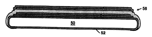
図4に示すように、ある実施態様の場合、上部、底部、及び、エッジ表面上に犠牲層52を堆積させた基板50が設けられる(ステップ54)。基板50は、1つ以上の半導体デバイスを備えたロジック階層と、1つ以上のコンタクトプラグが貫通している、上に重なる階層間誘電体層とを含む、半導体ウェーハ(例えば、シリコン・ウェーハ)とすることが可能である。犠牲層52は、例えば、ロジック階層またはコンタクトプラグ製作プロセス中に、従来の加熱炉プロセスによって形成可能な窒化珪素層または二酸化珪素層とすることが可能である。一般に、犠牲層52は、例えば、リフトオフ・プロセスによって基板のエッジ及び裏面から汚染物(例えば、Pb、Zr、Ti、及び、Ir)を除去するのに役立つはずである。さらに、犠牲層52は、重要なデバイス領域の電気特性を劣化させる可能性がある、基板50内への汚染物の拡散を阻止するはずである。
【0022】
他の実施態様の中には、犠牲層を含まないものもあり得る。
【0023】
図5を参照すると、強誘電体コンデンサ・スタック56は、基板50の上部表面上に配置される(ステップ58)。強誘電体コンデンサ・スタック56は、強誘電体コンデンサ10と同じ電極及び誘電体層を備えることが可能である。
【0024】
図6及び7に示すように、強誘電体デバイス材料38及び他の汚染物は、湿式エッチング・プロセスによって基板50の裏面、エッジ、及び、前面エッジ除外ゾーン表面から取り除くことが可能である(ステップ60)。すなわち、基板50は、自動化クリーニング・ステーション62(例えば、オーストリア、KaerntenのSEZ Semiconductor-Equipment Zubehoer Fuer die Halbleiterfertigung Gesellschaft m.b.Hから入手可能な自動化基板クリーナ)内に配置することが可能である。クリーニング・ステーション62には、基板50を保持するように構成された環状支持体64が含まれている。リング・ノズル66を通る加圧ガス(例えば、窒素ガス)の流出によって、基板50の下に真空が発生する。加圧ガスは、軸70まわりを回転するように構成されたシャフト68内に形成されたガス導管を通って、リング・ノズル66に送られる。クリーニング・ステーション62には、基板50の露出表面上にエッチング液74を吐出するように構成されたノズル72も含まれている。基板50の露出表面上に形成されるエッチング液の厚さ及び均一性は、少なくとも部分的には、ノズル72を通るエッチング液の流量、及び、基板50の回転速度によって決まる。実施時、基板50は、表を下にして支持体64に配置され、加圧ガスが、リング・ノズル66から噴射されて、基板50を所定位置に保持する真空が生じる。基板50が、軸70まわりを回転している間に、ノズル72からエッチング液74が吐出され、基板50の露出した裏面、エッジ、及び、前面エッジ除外ゾーン表面にわたって、ほぼ均一な膜が形成される。基板50の裏面、エッジ、及び、前面エッジ除外ゾーン表面のクリーニングが済むと、基板を回転させて乾燥させる。
【0025】
実施態様によっては、クリーニング・ステーション62内に基板50を配置する前に、強誘電体コンデンサ・スタック56の上に、保護フォトレジスト層を付着させることが可能なものもある。さらに、実施態様によっては、浴エッチング・プロセスによって、裏面、エッジ、及び、前面エッジ除外ゾーン表面から強誘電体デバイス材料を取り除くことが可能なものもある。
【0026】
図7に示すように、基板50の結果得られる裏面、エッジ、及び、前面エッジ除外ゾーン表面は、強誘電体コンデンサ10の形成中に生じた可能性のある汚染がほぼ皆無である。一般に、エッチング液74によって、全ての強誘電体デバイス材料汚染物(例えば、Pb、Zr、Ti、及び、Ir)が除去されるはずである。望ましいことには、エッチング液74によって、強誘電体デバイス汚染物は、例えば、Pb、Zr、Ti、及び、Irの残留表面濃度は、およそ1010cm-2以下程度にまで除去される。さらに、エッチング液74は、コンデンサ・スタック56の上に付着した保護フォトレジスト層(存在する場合)を侵蝕しないはずである。望ましい実施態様の場合、エッチング液74は、室温で有効に作用する。
【0027】
ある実施態様の場合、エッチング液74には、NH4F、HCl、及び、H2Oが1:1.6:xの体積比で含まれているが、ここで、xは1〜1,000にわたる値である。このエッチング化学反応は、PZTに関する選択性が強い。例えば、NH4F:HCl:H2Oの体積比が1:1.6:20の場合、コンデンサ・スタック及び犠牲層の構成材料に関して、下記のエッチング速度が得られた:
【0028】
【表2】
図8に示すように、NH4F:HCl:H2Oが1:1.6:xのエッチング液のPZTエッチング速度は、エッチング液中の酸の体積百分率と共に低下し、半対数プロットに従うことになる。例えば、厚さ250nmのPZT被膜のエッチングに基づくと、エッチング液比が1:1.6:20であれば、PZTのエッチング速度は70nm/秒になり、エッチング液比が1:1.6:40であれば、PZTのエッチング速度は10nm/秒になり、一方、PZTエッチング液比が1:1.6:100であれば、エッチング速度は5.5nm/秒になる。このデータに鑑みて、制御可能なPZTエッチング速度の実現には、約1:1.6:40〜1:1.6:100のエッチング液比が望ましい。このエッチング液比範囲内では、SiO2及びSi3N4のエッチング速度は、それぞれ、0.1nm/秒及び2.2nm/秒よりかなり低くなる。
【0030】
特定の理論に限定されるものではないが、NH4F、HCl、及び、H2Oエッチング化学薬品の選択性は、エッチング液中のフッ素と塩素の総合作用によって得られるものと考えられる。具体的には、エッチング液のフッ素化部分が、ZrO2及びTiO2を溶解し、塩素化部分がPbO2にエッチングを施すものと考えられる。従って、この実施態様の場合、HClとNH4Fが結合すると、強力で、選択的なPZTエッチングが行われることになる。例えば、このエッチング液をH2Oで希釈すると、PZTとSi、SiO2、Si3N4、及び、TiAlNとの間における強い選択性を特徴とする、エッチング液が得られる。
【0031】
フッ素ベースの酸及び塩素ベースの酸の混合物を含む他のエッチング用化学薬品をエッチング液74に利用することも可能である。
【0032】
実施態様によっては、エッチング液74は、下記エッチング用化学薬品の1つ、または、それらを2つ以上組み合わせたものによって実施可能な場合もある:
(i) HCl+H2O
(ii) HF+H2O
(iii)HNO3+H2O
(iv) HF+HCl+H2O
(v) NH4F+HCl+HNO3+H2O
(vi) HF+HCl+HNO3+H2O
(vii)HF+H2O2+HNO3+H2O
これらのエッチング用化学薬品は、それぞれ、選択的にPZTをエッチングする。例えば、エッチング用化学薬品(i)は、HCl:H2Oのエッチング液比が1:1であれば、PZTエッチング速度が2.9nm/秒になり、一方、エッチング用化学薬品(ii)は、HF:H2Oのエッチング液比が1:10であれば、PZTエッチング速度が8.4nm/秒になる。エッチング用化学薬品(vii)に関しては、H2O2が、エッチング液中のPbの酸化を促進することによって、Pbがメッキによって基板50に戻るのをほとんど阻止するものと考えられる。
【0033】
図9を参照すると、基板50の裏面、エッジ、及び、前面エッジ除外ゾーン表面のクリーニングが済むと(ステップ60)、コンデンサ・スタック56にエッチングを施して、強誘電体コンデンサ10のアレイが形成される(ステップ80)。コンデンサ・スタック56は、従来のエッチング・プロセスを利用して、エッチングを施すことが可能である。
【0034】
図10に示すように、コンデンサ・スタック56のエッチングが済むと(ステップ80)、犠牲層52にエッチングを施して、コンデンサ・スタック・エッチング・プロセス中に、犠牲層の露出表面に形成された可能性のあるエッチング残留汚染物40を除去することが可能である(ステップ82)。すなわち、Ir汚染物及び他のエッチング残留物(例えば、Pb、Zr、Ti、及び、有機物)は、犠牲層52が選択されたエッチング液で溶解する際、リフトオフによって除去することが可能である。一般に、犠牲層のエッチング化学薬品は、下方の基板材料(例えば、Si)を侵蝕することなく、犠牲層(例えば、Si3N4またはSiO2)を形成する材料にエッチングを施すはずである。望ましいことには、犠牲層のエッチング液によって、エッチング残留汚染物40も除去されるはずであるため、例えば、Pb、Zr、Ti、及び、Irの残留表面濃度は、およそ1010cm-2以下程度になる。望ましい実施態様の場合、犠牲層のエッチング液は、室温で有効に作用する。実施態様によっては、犠牲層のエッチング化学薬品が、PZTのエッチング化学薬品と同じものもある。例えば、HF及びH2Oの混合物を含むエッチング化学薬品は、PZTエッチングと犠牲層エッチングの両方に利用することが可能である。しかし、実施態様によっては、例えば、異なる汚染物濃度または異なるエッチング速度要件に適応するため、異なるエッチング化学薬品を利用することになる場合もあり得る。上述の一般的なガイドラインを満たす他の犠牲層のエッチング化学薬品を利用することも可能である。犠牲層のエッチング・ステップは、クリーニング・ステーション62や、別の適合するクリーニング装置において実施可能である。
【0035】
実施態様によっては、犠牲層のエッチング・ステップ後に、犠牲層52の一部が、基板50の裏面、エッジ、及び、前面エッジ除外ゾーン表面の上に付着したままである場合もあり得る。
【0036】
図11及び12に示すように、上述の強誘電体デバイス製作プロセス・モジュールは、標準CMOS集積回路製作プロセスに容易に組み込むことが可能である。ロジック階層と上に重なる階層間誘電体層及びコンタクトは、従来の業界標準のフロント・エンド半導体プロセス100を用いて、基板上に形成することが可能である(ステップ102)。フロント・エンド・プロセスによって、ウェーハの正面、裏面、及び、エッジにSiO2またはSi3N4層が生じる可能性がある。実施態様によっては、この層は、後続の汚染をコントロールするステップに関する犠牲層として利用することが可能である。次に、強誘電体コンデンサ及び上に重なる階層間誘電体層は、FeRAM専用プロセス・ツール106、共用FeRAMプロセス・ツール108、及び、自動化クリーニング・ステーション62を含む、上述のFeRAMプロセス・モジュール104を用いて、形成することが可能である。この実施態様の場合、まず、酸化障壁が標準のコンタクト上に形成される。次に、底部電極、PZT誘電体、上部電極、及び、ハードマスクが蒸着させられる。PZT誘電体は、1つのツールで蒸着させることが可能であり、電極及び拡散障壁は、もう1つのツールで形成することが可能である。ステップ112は、FeRAM専用ツール106を用いて実施されるのが望ましい。この時点において、基板は、自動化クリーニング・ステーション62に移送され、裏面、エッジ、及び、前面エッジ除外ゾーン表面をクリーニングすることが可能になる(ステップ114)。コンデンサ・スタックは、共用FeRAMプロセス・ツール108(例えば、リソグラフィック・ステッパ)でパターン形成され、コンデンサ・スタックは、専用エッチング・ツールでエッチングが施される(ステップ116)。必要があればエッチング後クリーニングを実施することが可能である(ステップ118)。側壁拡散障壁層26は、できれば、FeRAM専用ツール106によって、エッチングされたコンデンサ・スタックの上に形成することが、可能である(ステップ120)。基板は、再び、自動化クリーニング・ステーション62に移送され、裏面、エッジ、前面エッジ除外ゾーン表面をクリーニングすることが可能である(ステップ122)。窒化珪素エッチング停止層27及び階層間誘電体層32は、FeRAM共用ツール108を利用して、側壁拡散障壁層26の上に蒸着させられる(ステップ124)。コンタクトバイアが、FeRAM共用ツール108においてパターン形成され、パターン形成されたコンタクトバイアは、FeRAM専用ツール106における階層間誘電体層32を介してエッチングを施される(ステップ126)。基板は、次に、自動化クリーニング・ステーション62に移送され、裏面、エッジ、及び、前面エッジ除外ゾーン表面にクリーニングを施すことが可能になる(ステップ128)。エッチ・リカバリ及びアニール・プロセス、及び、コンタクト/相互接続形成プロセスが、FeRAM共用プロセス・ツール108で実施される(ステップ130、132)。基板は、次に、業界標準の半導体バック・エンド・プロセス134を利用して処理することが可能である(ステップ136)。
【0037】
FeRAM専用プロセスに特定のツールを割り当て、共用プロセスに他のツールを割り当てることと、FeRAM専用ツール106から共用ツール108に基板を移送する前に、汚染コントロール・プロセス・ステップを実施することとによって、上述のプロセスコントロールの方法は、強誘電体デバイス材料の導入による二次汚染の恐れを軽減し、同時に、強誘電体デバイス及び半導体デバイスのプロセス統合に関する生産効率を実現可能にする。
【0038】
特許請求の範囲の趣旨の範囲には、他の実施形態も存在する。
【0039】
例えば、実施態様によっては、従来の計測ステップは、共用計測ツールによって実施することが可能であり、この場合、基板がFeRAM専用ツールから共用計測装置に移送される前に、追加の汚染コントロール・ステップを実施すべきである。
【0040】
さらに、実施態様によっては、FeRAM共用ツールにおいて、バイアコンタクトエッチング・ステップ(ステップ126)を実施することが可能である。これらの実施態様の場合、後続の汚染コントロール・ステップ(ステップ128)は、実施されない。
【0041】
特許請求の範囲の趣旨の範囲には、さらにその他の実施態様も存在する。
【図面の簡単な説明】
【図1】それぞれの階層間誘電体層を通るように配置された1対の導電性プラグ間に結合されたFeRAMコンデンサの略断面側面図である。
【図2A】基板上に形成されるFeRAMコンデンサ層スタックの略断面側面図である。
【図2B】図2Aのコンデンサ層スタックにエッチングを施すことによって形成されるFeRAMコンデンサの略断面側面図である。
【図3】強誘電体デバイスを形成する方法のフロー図である。
【図4】基板の上部、底部、及び、エッジ表面の上に犠牲層が配置された、基板の略断面側面図である。
【図5】図4の基板上に形成されたコンデンサ層スタックの略断面側面図である。
【図6】図5の基板の裏面、エッジ、及び、前面エッジ除外ゾーンにエッチング液を付ける基板クリーニング装置に略断面側面図である。
【図7】エッチング液によって基板の裏面をクリーニングした後、図5のコンデンサ層スタックの略断面側面図である。
【図8】溶液内の酸の体積百分率の関数として描かれたNH4F、HCl、及び、H2Oのエッチング化学薬品に関するPZTエッチング速度のグラフである。
【図9】図7のコンデンサ層スタックにエッチングを施すことによって形成される複数の強誘電体コンデンサの略断面側面図である。
【図10】犠牲層にエッチング施すことによって、基板の底部表面、エッジ、及び、前面エッジ除外ゾーンから裏面汚染を除去した後の、図9の強誘電体コンデンサの略断面側面図である。
【図11】統合された強誘電デバイス・集積回路製作プロセスのフロー図である。
【図12】FeRAMプロセス・モジュールのFeRAM専用及び共用プロセス・ツールによるプロセスフローのブロック図である。
【符号の説明】
10 強誘電体デバイス
12 強誘電体層
14 底部電極
16 上部電極
33 底部表面
34 エッジ
35 前面エッジ除外ゾーン
36 基板
38 強誘電体デバイス材料
40 強誘電体デバイス材料
50 基板
52 犠牲層
62 クリーニング・ステーション
104 強誘電体デバイス・プロセス・モジュール
106 専用プロセス・ツール
108 共用プロセス・ツール[0001]
BACKGROUND OF THE INVENTION
The present invention relates to a system and method for controlling contaminants during the fabrication of embedded ferroelectric devices.
[0002]
[Prior art]
There are several trends in the semiconductor device manufacturing industry and the electronics industry that are driving the development of new material technologies today. First, devices such as personal handheld devices (eg, mobile phones and personal digital assistants) are becoming increasingly smaller and the amount of power required continues to decrease. Second, not only is it more compact and easier to carry, but such devices require more powerful computing power and larger on-chip memory. In view of these trends, there is a need in the industry to provide computing devices in which a significant amount of memory and logic functions are incorporated into the same semiconductor chip. This computing device includes a non-volatile memory so that the contents of the memory are retained even if the battery runs out. Examples of conventional non-volatile memory include electrically erasable PROM (“EEPROM”) and flash EEPROM. Table 1 illustrates the differences between the various memory types.
[0003]
Ferroelectric memory (FeRAM) is a ferroelectric material (eg, SrBi) that serves as a capacitor dielectric disposed between a bottom electrode and a top electrode. 2 Ta 2 O 9 (SBT) or Pb (Zr, Ti) O Three (PZT)). In general, a ferroelectric memory element is non-volatile due to the polarization state in which the material has bistability. In addition, ferroelectric memory devices are programmed at a relatively low voltage (eg, less than 5 volts), have a relatively fast access time (eg, less than 40 nanoseconds), and are operationally corrupted over many read and write cycles. Characterized by difficult points. These memory elements also have relatively low power consumption, can increase the recording density, and exhibit radiation resistance.
[0004]
[Table 1]
[Problems to be solved by the invention]
To integrate ferroelectric capacitors with standard complementary metal oxide semiconductor (CMOS) device technology, Si wafer fabrication facilities must introduce several new materials that contain non-standard metal components . The materials required to manufacture a typical ferroelectric capacitor stack include a PZT or SBT dielectric and one or more of the electrode materials Ir, Ru, Pt. Some of the metals present in these materials such as Ti, Ta, and Pt are utilized in mainstream Si wafer production lines. Other metals such as Pb, Zr, Sr, Bi, Ru, and Ir have not been introduced into the Si manufacturing flow. Thus, little is known about the effects of these materials on the yield, reliability, and electrical performance of CMOS-based devices. Furthermore, in the front-end technology requirements for wafer surface treatment, for known important metals such as Cu at the node of 180 nm technology, cm 2 9x10 per 9 Despite the fact that concentrations of less than atoms are defined, the exact limits for metal contaminants associated with FeRAM are not quantified.
[0006]
In general, the present invention is performed between a front-end process module (e.g., including logic element processes and contacts) and a back-end process module (e.g., mostly including a metallization process). The present invention relates to the fabrication of ferroelectric capacitors in FeRAM process modules. The FeRAM process module must be compatible with the front end process, including utilizing the W contact, which is currently standard in most logic flows, as the bottom contact of the capacitor. The thermal budget of FeRAM is sufficient so as not to affect the front end low resistance structures (tungsten plugs and silicide sources / drains and gates) used in most logic devices. Should be less. In addition, because transistors and other front end devices (eg, diodes) are sensitive to contamination, the FeRAM process module can directly or indirectly (eg, by diffusion within the chip) or indirectly such devices. Do not contaminate (for example, by cross contamination through shared devices). FeRAM devices and process modules should be compatible with standard back-end process flows. Therefore, the FeRAM process module must not increase the resistance of the metallized logic element, nor should it increase the parasitic capacitance between the metal and the transistor. In addition, FeRAM devices must not be degraded by standard back end process flows. This is an important issue. Ferroelectric capacitors have been found to be susceptible to hydrogen-induced degradation, and hydrogen or deuterium is used for most logic device back-end processes (eg, SiO 2). 2 , Si Three N Four And film formation of W by CVD, SiO 2 Via etching and forming gas annealing).
[0007]
In connection with contamination control, the contamination level of substrates processed by shared equipment (eg, steppers or metrology tools) should not be so high as to degrade device performance. Apart from processing errors, the main path of cross-contamination is the contact between the shared tool wafer handling system and the backside, edge and full edge exclusion zone surfaces of the substrate. For a typical FeRAM process flow, two processes are expected to lead to the worst contamination of the wafer backside and edges. (1) PZT or SBT film deposition and (2) dry etching of ferroelectric capacitor stacks. Therefore, to achieve the production efficiency gained from the use of shared equipment and facilities, removing undesirable elements from the backside, edge, and front edge exclusion zones of the substrate before using any shared process equipment. desirable.
[0008]
[Means for Solving the Problems]
In one aspect, the invention features a method of forming a ferroelectric device on a substrate having a top surface, a bottom surface, an edge, and a front edge exclusion zone. According to this method, a bottom electrode is formed on the top surface of the substrate. A ferroelectric layer is formed on the bottom electrode. An upper electrode is formed on the ferroelectric layer. To control contamination, ferroelectric device materials (e.g., contaminants associated with ferroelectrics such as Pb, Zr, Ti and contaminants associated with electrodes such as Ir) are applied to the bottom surface and edges of the substrate. Is removed by selective etching.
[0009]
Implementations of the invention can include one or more of the following features.
[0010]
The ferroelectric device material is removed from the substrate bottom surface and edge by selective etching using an etchant comprising an acid containing fluorine, an acid containing chlorine, or an acid containing both. In some embodiments, the etchant includes NH. Four A mixture of F and HCl is included. The etchant contains NH with a volume ratio of about 1: 1.6. Four F: HCl can be included. The etchant further includes a diluent (eg, H 2 O) can be included. In some embodiments, the etchant includes NH with a volume ratio of about 1: 1.6: x. Four F: HCl: H 2 O is included, where x is preferably a value ranging from about 20 to about 1,000, more preferably a value ranging from about 40 to about 100.
[0011]
In some embodiments, the ferroelectric device material is HCl and H. 2 O; HF and H 2 O; HNO Three And
[0012]
The ferroelectric device material can also be selectively etched away from the front edge exclusion zone of the substrate.
[0013]
In some embodiments, the substrate includes a sacrificial layer deposited over the bottom surface and edges of the substrate. The sacrificial layer can include silicon nitride or silicon dioxide. The sacrificial layer can be etched using an etchant containing fluorine (for example, HF). The sacrificial layer can extend over the front edge exclusion zone of the substrate. The sacrificial layer is preferably etched after the ferroelectric capacitor structure is formed.
[0014]
In another aspect, the present invention provides a ferroelectric device process module that includes one or more dedicated process tools, one or more shared process tools, and one or more cleaning stations. Features. Dedicated process tools are dedicated to the processing of ferroelectric devices only. Shared process tools have been assigned to both ferroelectric device processing and standard semiconductor device processing. The cleaning station is configured to remove ferroelectric device contaminants from the substrate before the substrate is transferred from the dedicated process tool to the shared process tool.
[0015]
Other features and advantages of the invention will become apparent from the following description, including the drawings and the claims.
[0016]
DETAILED DESCRIPTION OF THE INVENTION
In the following description, similar reference numbers are used to identify similar components. Furthermore, the drawings are intended to illustrate an overview of the main features of an exemplary embodiment. The drawings are not intended to depict every feature of an actual embodiment, nor are they intended to represent the relative dimensions of the depicted components, and are not drawn to scale. Absent.
[0017]
Referring to FIG. 1, in one embodiment, an integrated circuit
[0018]
As shown in FIGS. 2A and 2B, during the formation of the
[0019]
As will be described in detail later, the
[0020]
3 to 10, first, referring to FIGS. 3 and 4, the
[0021]
As shown in FIG. 4, in one embodiment, a
[0022]
Some other embodiments may not include a sacrificial layer.
[0023]
Referring to FIG. 5, a
[0024]
As shown in FIGS. 6 and 7, the
[0025]
In some embodiments, a protective photoresist layer can be deposited over the
[0026]
As shown in FIG. 7, the resulting backside, edge, and front edge exclusion zone surfaces of the
[0027]
In some embodiments, the
[0028]
[Table 2]
As shown in FIG. Four F: HCl: H 2 The PZT etch rate of the etchant with O = 1: 1.6: x decreases with the volume percentage of acid in the etchant and follows a semi-log plot. For example, based on etching of a PZT film having a thickness of 250 nm, if the etchant ratio is 1: 1.6: 20, the etch rate of PZT is 70 nm / second, and the etchant ratio is 1: 1.6: If it is 40, the etching rate of PZT is 10 nm / second, while if the PZT etchant ratio is 1: 1.6: 100, the etching rate is 5.5 nm / second. In view of this data, an etchant ratio of about 1: 1.6: 40 to 1: 1.6: 100 is desirable to achieve a controllable PZT etch rate. Within this etchant ratio range, SiO 2 And Si Three N Four The etch rates of are significantly lower than 0.1 nm / second and 2.2 nm / second, respectively.
[0030]
Without being limited to a particular theory, NH Four F, HCl, and H 2 The selectivity of the O-etching chemical is considered to be obtained by the combined action of fluorine and chlorine in the etchant. Specifically, the fluorinated portion of the etching solution is ZrO. 2 And TiO 2 And the chlorinated part is PbO 2 It is thought that etching is performed on the surface. Thus, in this embodiment, HCl and NH Four When F is combined, a strong and selective PZT etch will be performed. For example, this etching solution is H 2 When diluted with O, PZT and Si, SiO 2 , Si Three N Four And an etchant characterized by strong selectivity with TiAlN.
[0031]
Other etch chemistries including mixtures of fluorine-based acids and chlorine-based acids may be utilized for the
[0032]
In some embodiments, the
(I) HCl + H 2 O
(Ii) HF + H 2 O
(Iii) HNO Three + H 2 O
(Iv) HF + HCl + H 2 O
(V) NH Four F + HCl + HNO Three + H 2 O
(Vi) HF + HCl + HNO Three + H 2 O
(Vii) HF + H 2 O 2 + HNO Three + H 2 O
Each of these etch chemistries selectively etch PZT. For example, the etching chemical (i) is HCl: H 2 If the etchant ratio of O is 1: 1, the PZT etch rate is 2.9 nm / sec, while the etching chemical (ii) is HF: H 2 If the O etchant ratio is 1:10, the PZT etch rate is 8.4 nm / sec. For etching chemicals (vii) 2 O 2 However, it is considered that Pb is almost prevented from returning to the
[0033]
Referring to FIG. 9, once the backside, edge, and front edge exclusion zone surfaces of the
[0034]
As shown in FIG. 10, once the
[0035]
In some embodiments, after the sacrificial layer etching step, a portion of the
[0036]
As shown in FIGS. 11 and 12, the ferroelectric device fabrication process module described above can be easily incorporated into a standard CMOS integrated circuit fabrication process. Interlevel dielectric layers and contacts overlying the logic hierarchy can be formed on the substrate using a conventional industry standard front end semiconductor process 100 (step 102). Front-end process allows SiO on the front, back and edges of the wafer 2 Or Si Three N Four Layers can occur. In some embodiments, this layer can be used as a sacrificial layer for the subsequent step of controlling contamination. Next, the ferroelectric capacitor and the overlying interlevel dielectric layer include the
[0037]
By assigning a specific tool to the FeRAM dedicated process and assigning other tools to the shared process, and performing a contamination control process step prior to transferring the substrate from the FeRAM
[0038]
Other embodiments exist within the scope of the claims.
[0039]
For example, in some embodiments, conventional metrology steps can be performed by a shared metrology tool, in which case an additional contamination control step is performed before the substrate is transferred from the FeRAM dedicated tool to the shared metrology tool. Should be implemented.
[0040]
Further, in some implementations, a via contact etch step (step 126) can be performed in the FeRAM shared tool. In these embodiments, the subsequent contamination control step (step 128) is not performed.
[0041]
Still other embodiments exist within the scope of the appended claims.
[Brief description of the drawings]
FIG. 1 is a schematic cross-sectional side view of a FeRAM capacitor coupled between a pair of conductive plugs disposed through respective interlevel dielectric layers.
FIG. 2A is a schematic cross-sectional side view of an FeRAM capacitor layer stack formed on a substrate.
2B is a schematic cross-sectional side view of an FeRAM capacitor formed by etching the capacitor layer stack of FIG. 2A.
FIG. 3 is a flow diagram of a method of forming a ferroelectric device.
FIG. 4 is a schematic cross-sectional side view of a substrate with a sacrificial layer disposed on the top, bottom, and edge surfaces of the substrate.
FIG. 5 is a schematic cross-sectional side view of a capacitor layer stack formed on the substrate of FIG. 4;
6 is a schematic cross-sectional side view of the substrate cleaning apparatus for applying an etchant to the back surface, edge, and front edge exclusion zone of the substrate of FIG. 5;
7 is a schematic cross-sectional side view of the capacitor layer stack of FIG. 5 after cleaning the backside of the substrate with an etchant.
FIG. 8 NH depicted as a function of volume percentage of acid in solution Four F, HCl, and
9 is a schematic cross-sectional side view of a plurality of ferroelectric capacitors formed by etching the capacitor layer stack of FIG. 7. FIG.
10 is a schematic cross-sectional side view of the ferroelectric capacitor of FIG. 9 after removing backside contamination from the bottom surface, edge, and front edge exclusion zone of the substrate by etching the sacrificial layer.
FIG. 11 is a flow diagram of an integrated ferroelectric device / integrated circuit fabrication process.
FIG. 12 is a block diagram of the process flow of FeRAM process modules with dedicated FeRAM and shared process tools.
[Explanation of symbols]
10 Ferroelectric devices
12 Ferroelectric layer
14 Bottom electrode
16 Upper electrode
33 Bottom surface
34 edge
35 Front edge exclusion zone
36 substrates
38 Ferroelectric device materials
40 Ferroelectric device materials
50 substrates
52 Sacrificial layer
62 Cleaning Station
104 Ferroelectric device process module
106 Dedicated process tool
108 Shared Process Tool
Claims (7)
前記基板の少なくとも前記底部表面とエッジと基板前面エッジ除外ゾーンとの上に犠牲層を堆積するステップと、
前記基板の上部表面の上に底部電極を形成するステップと、
前記底部電極の上に強誘電体層を形成するステップと、
前記強誘電体層の上に上部電極を形成するステップと、
前記基板の前記底部表面及び前記エッジの前記犠牲層の少なくとも一部をエッチングして、該底部表面と前記エッジと前記基板前面エッジ除外ゾーンの強誘電体デバイス材料を除去する第1のクリーニングステップと、
前記第1のクリーニングステップより後に、前記底部電極、前記強誘電体層および前記上部電極を含むコンデンサスタックをエッチングして、強誘電体コンデンサのアレイを形成するパターニングステップと、
前記パターニングステップより後に、前記基板の前記底部表面及び前記エッジの前記犠牲層の残部の少なくとも一部をエッチングして、該底部表面と前記エッジと前記基板前面エッジ除外ゾーンにおける犠牲層の露出表面におけるエッチング残留汚染物を除去する第2のクリーニングステップと
を含んでなる方法。A method of forming a ferroelectric device on a substrate comprising a top surface, a bottom surface, an edge, and a front edge exclusion zone, comprising:
Depositing a sacrificial layer over at least the bottom surface and edge of the substrate and the substrate front edge exclusion zone ;
Forming a bottom electrode on the top surface of the substrate;
Forming a ferroelectric layer on the bottom electrode;
Forming an upper electrode on the ferroelectric layer;
A first cleaning step of etching at least a portion of the bottom surface of the substrate and the sacrificial layer at the edge to remove ferroelectric device material from the bottom surface, the edge and the substrate front edge exclusion zone ; ,
Etching the capacitor stack including the bottom electrode, the ferroelectric layer, and the top electrode after the first cleaning step to form an array of ferroelectric capacitors;
After the patterning step, etch at least a portion of the bottom surface of the substrate and the remainder of the sacrificial layer at the edge to expose the bottom surface, the edge, and the exposed surface of the sacrificial layer in the substrate front edge exclusion zone. And a second cleaning step to remove residual etching contaminants .
前記第3のクリーニングステップより後に、半導体バック・エンド・プロセスを利用するステップとUtilizing a semiconductor back-end process after the third cleaning step;
をさらに含む請求項6に記載の強誘電体デバイスを形成する方法。A method of forming a ferroelectric device according to claim 6 further comprising:
Applications Claiming Priority (2)
| Application Number | Priority Date | Filing Date | Title |
|---|---|---|---|
| US09/925201 | 2001-08-08 | ||
| US09/925,201 US6709875B2 (en) | 2001-08-08 | 2001-08-08 | Contamination control for embedded ferroelectric device fabrication processes |
Publications (3)
| Publication Number | Publication Date |
|---|---|
| JP2003158115A JP2003158115A (en) | 2003-05-30 |
| JP2003158115A5 JP2003158115A5 (en) | 2005-10-27 |
| JP4285954B2 true JP4285954B2 (en) | 2009-06-24 |
Family
ID=25451373
Family Applications (1)
| Application Number | Title | Priority Date | Filing Date |
|---|---|---|---|
| JP2002232065A Expired - Fee Related JP4285954B2 (en) | 2001-08-08 | 2002-08-08 | Contamination control method for embedded ferroelectric device fabrication process |
Country Status (4)
| Country | Link |
|---|---|
| US (1) | US6709875B2 (en) |
| JP (1) | JP4285954B2 (en) |
| KR (1) | KR100880109B1 (en) |
| DE (1) | DE10231192A1 (en) |
Families Citing this family (17)
| Publication number | Priority date | Publication date | Assignee | Title |
|---|---|---|---|---|
| JP5132859B2 (en) * | 2001-08-24 | 2013-01-30 | ステラケミファ株式会社 | Micro-processed surface treatment liquid for glass substrates with multiple components |
| US6767750B2 (en) * | 2001-12-31 | 2004-07-27 | Texas Instruments Incorporated | Detection of AIOx ears for process control in FeRAM processing |
| JP2004087691A (en) * | 2002-08-26 | 2004-03-18 | Fujitsu Ltd | Method for removing gate insulation film |
| US6876021B2 (en) * | 2002-11-25 | 2005-04-05 | Texas Instruments Incorporated | Use of amorphous aluminum oxide on a capacitor sidewall for use as a hydrogen barrier |
| KR100504693B1 (en) * | 2003-02-10 | 2005-08-03 | 삼성전자주식회사 | Ferroelectric memory device and method for fabricating the same |
| US20050037521A1 (en) * | 2003-08-15 | 2005-02-17 | Uwe Wellhausen | Methods and apparatus for processing semiconductor devices by gas annealing |
| JP4610486B2 (en) * | 2003-12-26 | 2011-01-12 | 富士通セミコンダクター株式会社 | Semiconductor device and method for manufacturing semiconductor device |
| US7180141B2 (en) * | 2004-12-03 | 2007-02-20 | Texas Instruments Incorporated | Ferroelectric capacitor with parallel resistance for ferroelectric memory |
| KR100722128B1 (en) * | 2005-12-28 | 2007-05-25 | 동부일렉트로닉스 주식회사 | Fabricating method of semiconductor device |
| US7572698B2 (en) * | 2006-05-30 | 2009-08-11 | Texas Instruments Incorporated | Mitigation of edge degradation in ferroelectric memory devices through plasma etch clean |
| JP5109395B2 (en) * | 2007-02-14 | 2012-12-26 | 富士通セミコンダクター株式会社 | Semiconductor device and manufacturing method thereof |
| US8415650B2 (en) * | 2009-07-02 | 2013-04-09 | Actel Corporation | Front to back resistive random access memory cells |
| US20110297088A1 (en) * | 2010-06-04 | 2011-12-08 | Texas Instruments Incorporated | Thin edge carrier ring |
| CN103087718B (en) * | 2013-01-16 | 2014-12-31 | 四川大学 | Etching solution for performing wet etching on lanthanum nickelate film and ferroelectric film/lanthanum nickelate composite film and preparation method thereof |
| US9041919B2 (en) | 2013-02-18 | 2015-05-26 | Globalfoundries Inc. | Infrared-based metrology for detection of stress and defects around through silicon vias |
| JP2016184677A (en) * | 2015-03-26 | 2016-10-20 | 株式会社ユーテック | Method of manufacturing ferroelectric film |
| JP2017098367A (en) * | 2015-11-20 | 2017-06-01 | 東京エレクトロン株式会社 | Substrate processing method |
Family Cites Families (18)
| Publication number | Priority date | Publication date | Assignee | Title |
|---|---|---|---|---|
| US5046043A (en) | 1987-10-08 | 1991-09-03 | National Semiconductor Corporation | Ferroelectric capacitor and memory cell including barrier and isolation layers |
| US5258093A (en) * | 1992-12-21 | 1993-11-02 | Motorola, Inc. | Procss for fabricating a ferroelectric capacitor in a semiconductor device |
| US6051858A (en) | 1996-07-26 | 2000-04-18 | Symetrix Corporation | Ferroelectric/high dielectric constant integrated circuit and method of fabricating same |
| US6114254A (en) * | 1996-10-15 | 2000-09-05 | Micron Technology, Inc. | Method for removing contaminants from a semiconductor wafer |
| US5807774A (en) | 1996-12-06 | 1998-09-15 | Sharp Kabushiki Kaisha | Simple method of fabricating ferroelectric capacitors |
| US5773314A (en) | 1997-04-25 | 1998-06-30 | Motorola, Inc. | Plug protection process for use in the manufacture of embedded dynamic random access memory (DRAM) cells |
| JPH10340893A (en) * | 1997-06-09 | 1998-12-22 | Sony Corp | Method for etching electronic thin-film material |
| US6143476A (en) | 1997-12-12 | 2000-11-07 | Applied Materials Inc | Method for high temperature etching of patterned layers using an organic mask stack |
| US6225156B1 (en) * | 1998-04-17 | 2001-05-01 | Symetrix Corporation | Ferroelectric integrated circuit having low sensitivity to hydrogen exposure and method for fabricating same |
| US6174735B1 (en) | 1998-10-23 | 2001-01-16 | Ramtron International Corporation | Method of manufacturing ferroelectric memory device useful for preventing hydrogen line degradation |
| US6140672A (en) * | 1999-03-05 | 2000-10-31 | Symetrix Corporation | Ferroelectric field effect transistor having a gate electrode being electrically connected to the bottom electrode of a ferroelectric capacitor |
| JP3395696B2 (en) * | 1999-03-15 | 2003-04-14 | 日本電気株式会社 | Wafer processing apparatus and wafer processing method |
| JP2000315670A (en) * | 1999-04-30 | 2000-11-14 | Nec Corp | Cleaning method of semiconductor substrate |
| KR100329759B1 (en) * | 1999-06-30 | 2002-03-25 | 박종섭 | Method for forming ferroelectric capacitor |
| JP2001068463A (en) * | 1999-08-31 | 2001-03-16 | Hitachi Ltd | Method for mass production of semiconductor integrated circuit device |
| US6261892B1 (en) * | 1999-12-31 | 2001-07-17 | Texas Instruments Incorporated | Intra-chip AC isolation of RF passive components |
| JP2002231676A (en) * | 2001-01-30 | 2002-08-16 | Toshiba Corp | Wafer-cleaning method and device |
| JP2002353182A (en) * | 2001-05-25 | 2002-12-06 | Mitsubishi Electric Corp | Rinsing method and rinsing device for semiconductor device, and manufacturing method for the semiconductor device |
-
2001
- 2001-08-08 US US09/925,201 patent/US6709875B2/en not_active Expired - Fee Related
-
2002
- 2002-07-10 DE DE10231192A patent/DE10231192A1/en not_active Withdrawn
- 2002-08-07 KR KR1020020046627A patent/KR100880109B1/en not_active IP Right Cessation
- 2002-08-08 JP JP2002232065A patent/JP4285954B2/en not_active Expired - Fee Related
Also Published As
| Publication number | Publication date |
|---|---|
| KR100880109B1 (en) | 2009-01-21 |
| DE10231192A1 (en) | 2003-03-06 |
| JP2003158115A (en) | 2003-05-30 |
| US20030036209A1 (en) | 2003-02-20 |
| US6709875B2 (en) | 2004-03-23 |
| KR20030014627A (en) | 2003-02-19 |
Similar Documents
| Publication | Publication Date | Title |
|---|---|---|
| JP4285954B2 (en) | Contamination control method for embedded ferroelectric device fabrication process | |
| US6734477B2 (en) | Fabricating an embedded ferroelectric memory cell | |
| US6534809B2 (en) | Hardmask designs for dry etching FeRAM capacitor stacks | |
| US6656748B2 (en) | FeRAM capacitor post stack etch clean/repair | |
| US6174766B1 (en) | Semiconductor device and method of manufacturing the semiconductor device | |
| JP2003318371A (en) | Method of etching capacitor stack associated with ferroelectric memory cell | |
| JP2001223342A (en) | Method of planarizing conductive plugs underlying ferroelectric capacitors of semiconductor device | |
| JP2001217400A (en) | Method of reinforcing adhesion of conductive barrier layer to conductive plug and contact in lower layer in semiconductor device | |
| US6211034B1 (en) | Metal patterning with adhesive hardmask layer | |
| JP2001230382A (en) | Contact etching containing no hydrogen for forming ferroelectric capacitor | |
| JP2001210798A (en) | Use of insulating and conductive barrier for protecting capacitor structure | |
| US20030176073A1 (en) | Plasma etching of Ir and PZT using a hard mask and C12/N2/O2 and C12/CHF3/O2 chemistry | |
| US11856788B2 (en) | Semiconductor device and method of fabricating the same | |
| JP3645144B2 (en) | Manufacturing method of semiconductor device | |
| JP4010819B2 (en) | Manufacturing method of semiconductor device | |
| KR100832683B1 (en) | Semiconductor device manufacturing method | |
| JP4838613B2 (en) | Manufacturing method of semiconductor device | |
| JP4848402B2 (en) | Manufacturing method of semiconductor integrated circuit device | |
| US7892916B2 (en) | Semiconductor device and fabricating method thereof | |
| JP2002016053A (en) | Method of manufacturing semiconductor device | |
| JP4199232B2 (en) | Mass production method of semiconductor integrated circuit device | |
| JP2000133642A (en) | ETCHING LIQUID FOR REMOVING Bi-BASED OXIDE CERAMIC, MANUFACTURE OF INTEGRATED CIRCUIT AND CLEANING OF TOOL USED IN TREATMENT OF Bi-BASED OXIDE CERAMIC | |
| US7927993B2 (en) | Cross-contamination control for semiconductor process flows having metal comprising gate electrodes | |
| US6825116B2 (en) | Method for removing structures | |
| US20090197421A1 (en) | Chemistry and compositions for manufacturing integrated circuits |
Legal Events
| Date | Code | Title | Description |
|---|---|---|---|
| A521 | Request for written amendment filed |
Free format text: JAPANESE INTERMEDIATE CODE: A523 Effective date: 20050802 |
|
| A621 | Written request for application examination |
Free format text: JAPANESE INTERMEDIATE CODE: A621 Effective date: 20050802 |
|
| A977 | Report on retrieval |
Free format text: JAPANESE INTERMEDIATE CODE: A971007 Effective date: 20071107 |
|
| A131 | Notification of reasons for refusal |
Free format text: JAPANESE INTERMEDIATE CODE: A131 Effective date: 20071109 |
|
| A601 | Written request for extension of time |
Free format text: JAPANESE INTERMEDIATE CODE: A601 Effective date: 20080123 |
|
| A602 | Written permission of extension of time |
Free format text: JAPANESE INTERMEDIATE CODE: A602 Effective date: 20080128 |
|
| A521 | Request for written amendment filed |
Free format text: JAPANESE INTERMEDIATE CODE: A523 Effective date: 20080509 |
|
| A131 | Notification of reasons for refusal |
Free format text: JAPANESE INTERMEDIATE CODE: A131 Effective date: 20080819 |
|
| A521 | Request for written amendment filed |
Free format text: JAPANESE INTERMEDIATE CODE: A523 Effective date: 20081119 |
|
| TRDD | Decision of grant or rejection written | ||
| A01 | Written decision to grant a patent or to grant a registration (utility model) |
Free format text: JAPANESE INTERMEDIATE CODE: A01 Effective date: 20090303 |
|
| A01 | Written decision to grant a patent or to grant a registration (utility model) |
Free format text: JAPANESE INTERMEDIATE CODE: A01 |
|
| A61 | First payment of annual fees (during grant procedure) |
Free format text: JAPANESE INTERMEDIATE CODE: A61 Effective date: 20090324 |
|
| FPAY | Renewal fee payment (event date is renewal date of database) |
Free format text: PAYMENT UNTIL: 20120403 Year of fee payment: 3 |
|
| R150 | Certificate of patent or registration of utility model |
Free format text: JAPANESE INTERMEDIATE CODE: R150 |
|
| LAPS | Cancellation because of no payment of annual fees |