JP4283003B2 - Power line communication signal transmission circuit and modulation signal output circuit - Google Patents
Power line communication signal transmission circuit and modulation signal output circuit Download PDFInfo
- Publication number
- JP4283003B2 JP4283003B2 JP2003024089A JP2003024089A JP4283003B2 JP 4283003 B2 JP4283003 B2 JP 4283003B2 JP 2003024089 A JP2003024089 A JP 2003024089A JP 2003024089 A JP2003024089 A JP 2003024089A JP 4283003 B2 JP4283003 B2 JP 4283003B2
- Authority
- JP
- Japan
- Prior art keywords
- circuit
- power line
- modulation
- output
- line communication
- Prior art date
- Legal status (The legal status is an assumption and is not a legal conclusion. Google has not performed a legal analysis and makes no representation as to the accuracy of the status listed.)
- Expired - Lifetime
Links
Images


Landscapes
- Cable Transmission Systems, Equalization Of Radio And Reduction Of Echo (AREA)
Description
【0001】
【発明の属する技術分野】
本発明は、電力線通信を利用した負荷制御システム、監視・計測システム、自動検針システム、データ伝送システム等に利用される電力線通信用信号送信回路および電力線通信用信号送信回路用の変調信号出力回路に関する。
【0002】
【従来の技術】
電力線を用いて信号を伝送する電力線搬送方式は、使用する信号(搬送波)周波数が低いほど、伝達率が良く、伝達特性が安定する。
【0003】
この理由により、情報量が少ない自動検針分野、負荷監視制御分野には、可聴周波数帯(100Hz〜10kHz)を使用した電力線搬送方式が利用されている。
【0004】
一方、このような電力線搬送方式においては、使用する信号周波数が低いほど結合カプラの形状が大きくなる傾向に有る。また、電力線のインピーダンスが低くなる特性により、信号増幅器に供給する電源パワーが大きくなる傾向に有る。つまり、可聴周波数帯を使用することは、伝送の信頼性は高いものの、通信機器の形状を大きくし、コストを下げられないという問題を持つ。
【0005】
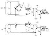
図5を用いて、従来の一般的な電力線通信用送信回路の構成を説明する。従来の一般的電力線通信用送信回路は、変調信号出力回路5の変調信号Smを、線形増幅器7で増幅し、結合カプラ8を介して電力線1に供給するように構成されている。電力線1から増幅器用電源9を取っている。信号入力側へ交流電力波が及ぶことを阻止するとともに交流電力線路への信号結合のための結合カプラ8として、図5(a)に示されるようなトランスTとコンデンサCとによる結合カプラを使用すること(例えば、特許文献1参照)、または図5(b)に示されるようなトランスTとリアクトルLとコンデンサCの共振回路とによる結合カプラを使用する(例えば、特許文献2参照)のが一般的であった。
【0006】
図5(a)のコンデンサを用いた結合カプラは、使用する周波数帯域を広く取れるが、結合効率が悪く、また図5(b)のリアクトルLとコンデンサCの共振回路を用いた結合カプラでは結合効率は比較的良くなるが、共振回路を使用するので使用する周波数帯域が制限されるという問題を有している。
【0007】
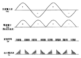
これらの課題を解決するために、図6に示すような、整流回路2、21と抵抗器3とスイッチング素子41からなる簡素化した回路構成の電力線通信用送信回路が提案されている(例えば、特許文献3参照)が、交流電力波を図6(a)のように全波整流、または図6(b)のように半波整流して得た電圧Vdcの振幅は一定でなく、この電圧を、抵抗器3を介してスイッチングした信号電流の値も一定値にはならないので、多値振幅変調などには適用できないという問題が有る。
【0008】
すなわち、従来の図6(a)に示される回路の各部の波形を図7に示す。変調信号Smは、交流電力波Vacを全波整流した電源電圧Vdcにより増幅され、出力電流波Ioが電力線1へ重畳されることになる。電源電圧Vdcは常に変動しているので、この電源電圧を変調信号でスイッチングした出力電流波Ioも電源電圧Vdcの変動にともなって変動する。
【0009】
このような変動する出力電流値Ioを生じる回路は、一定の電流値が必要な多値振幅変調などには適用できないという問題が有る。
【0010】
【特許文献1】
特開昭61−198927号公報(第1図)
【特許文献2】
特開昭63―2431号公報(第2図)
【特許文献3】
実公平7―35464号公報(第5図)
【0011】
【発明が解決しようとする課題】
本発明は、このような点に鑑み、回路構成の少ない、線形な信号増幅および使用周波数の帯域制限のない電力線路への信号結合可能な電力線通信用信号送信回路およびこの電力線通信用信号送信回路に結合される送信データを変調する位相変調回路を実現することを目的とする。
【0012】
【課題を解決するための手段】
上記目的を達成するために、本発明は、交流電力線路に対して、整流回路と、整流回路に直列接続した電流増幅回路素子および電流検出抵抗ならびに電流増幅回路素子の動作を制御する演算増幅器を有し、フィードバック回路を有する電圧―電流変換回路を直接接続し、これに通信用変調信号を入力するようにした。
【0013】
また、本発明は、上記整流回路を全波整流回路とした。さらに、本発明は、演算増幅器の入力側にオフセット回路を挿入した。
【0014】
さらに、本発明は、電力線通信用信号送信回路に結合される送信データを変調する位相変調回路であって、交流波の極性に応じて変調データを反転させるデータ反転回路を備えた。
【0015】
さらにまた、本発明は、位相変調回路を、交流波の極性を判定する極性判定回路、交流波の極性に応じて変調データを反転させるデータ反転回路、送信フィルタ、搬送波変調回路から成るようにした。
【0016】
【発明の実施の形態】
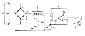
本発明の実施の形態を、実施例にもとづき図面を参照して説明する。図1は交流電力線路へ通信信号を結合する信号増幅・結合回路を備えた電力線通信用信号送信回路を示す。
【0017】
図1に示すように、本発明にかかる電力線通信用信号送信回路は、電力線1に接続された全波整流回路2と、全波整流回路2の一方の出力端子(例えば+端子)に接続された保護抵抗3と、保護抵抗3に直列に接続された電圧−電流変換回路4と、電圧−電流変換回路4の一方の入力端子に入力される変調信号出力回路5とから構成される。
【0018】
電圧−電流変換回路4は、電流増幅回路素子41と、電流検出抵抗42と、演算増幅器(OPアンプ)43と、フィードバック回路44とから構成される。電流増幅回路素子41は、全波整流回路2の直流出力端子間に接続された保護抵抗3と電流検出抵抗42とに直列に接続され、演算増幅器43の出力によって制御される。電流検出抵抗42は、電流増幅回路素子41と全波整流回路2の他方の出力端子(例えば−端子)との間に直列に接続される。演算増幅器43は、一方の入力端子(例えば+端子)に変調信号Smが入力され、他方の入力端子(例えば−端子)に電流増幅回路素子41と電流検出抵抗42の接続点の電圧Vfがフィードバック回路44を介して入力され、出力端子が電流増幅回路素子41の制御端子に接続される。
【0019】
変調信号出力回路5は、交流搬送波fcを送信データで変調した変調信号Smを出力する回路である。この変調信号Smは、電圧―電流変換回路4、全波整流回路2を経て交流電力線路1の交流電力波Vacに重畳される。
【0020】
電圧―電流変換回路4は、信号増幅回路と信号結合回路(カプラ)の機能を合わせ持つ回路を構成しており、交流電力波Vacを整流した電圧源に直接接続される。
【0021】
本発明において、電圧―電流変換回路4を使用して電流検出抵抗42の電圧Vfをフイードバックしているのは、変調信号Smを重畳する電源が、直流でなく電圧が変動する整流交流波であるので、変調信号Smを線形増幅するためである。すなわち、電圧−電流変換回路4は、電源電圧Vdcが低い値のときには電流増幅回路素子41に大きな制御信号を送出して出力電流波Ioが一定の振幅を維持するように動作し、電源電圧Vdcが大きな値のときには電流増幅回路素子41に小さな制御信号を送出して出力電流波Ioが一定の振幅を維持するように動作することによって、一定の振幅の出力電流波Ioを出力するように動作する。
【0022】
この回路には全体として帯域制限要素がないので、広帯域信号の増幅と電力線路への信号の重畳が可能となる。
【0023】
また、線形な信号増幅との結合であるので、QAM方式等の多値振幅変調にも適用可能であり、低コストで高性能な電力線通信機器を実現することができる。
【0024】
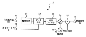
図2を用いて、変調信号出力回路5の構成例を説明する。変調信号出力回路5は、極性判定回路51と、データ反転回路52と、送信フィルタ53と、変調回路54と、搬送波発信回路55と、オフセット成分加算回路56と、交流電力波入力端子T1と、送信データ列入力端子T2と、変調信号出力端子T3とから構成される。
【0025】
極性判定回路51は、交流電力波入力端子T1から入力される交流電力波Vacの極性を判定する回路である。データ反転回路52は、送信データ入力端子T2から入力される送信データ列Dに、交流電力波Vacの極性が正負いずれか、例えば負の時に反転させる極性反転処理を施す回路である。送信フィルタ53は、極性反転処理を施した送信データDrのノイズ成分を取り除く回路である。変調回路54は、反転処理後の送信データDrにより搬送波fcを変調する回路である。搬送波発信回路55は、搬送波fcを出力する回路である。
【0026】
オフセット成分加算回路56は、変調回路54からの反転処理送信データDrにより変調された搬送波fcにオフセット成分を加算して変調信号Smとして変調信号出力端子T3から出力する回路である。すなわち、電圧−電流変換回路4で変調信号Smを忠実に電流増幅するためには、電流増幅回路素子41の制御端子へ入力される変調信号出力回路5の変調信号Smは単一方向の電流でなければならず、変調回路54の出力信号にオフセット電流成分を付加することが必要となる。また、電流増幅回路素子41の制御端子に常時オフセット電流が流れることを避けるために、オフセット成分加算回路56は、変調信号Smを出力するときのみオフセット電流を加算するように作用する。
【0027】
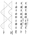
本発明の送信回路を用いて変調信号を搬送波に乗せて出力する場合、負のサイクルでは変調信号は位相が反転されて重畳されてしまう。よって、位相情報を含む変調搬送波を電力線に重畳させるには、負のサイクルにおいては予め符号を反転させて出力する必要がある。
【0028】
すなわち、図3に示すように、送信データ列Dは、交流電力波Vacの極性が正と判定された場合にはそのまま通過し、負と判定された場合にはデータ反転回路52においてデータ反転処理が施された反転処理送信データDrとされて、送信フィルタ53に送られる。
【0029】
この変調信号出力回路5は、図1に示されるように整流回路として全波整流回路を使用する場合で、位相情報を含む変調方式(PSK方式)や位相情報と振幅情報を含む変調方式(QAM方式)で変調する場合に採用され、QAM方式等の多値振幅変調波を、図1に示される電力線通信用信号送信回路に重畳することができる。
【0030】
図1に示した電力線通信用信号送信回路における各部の波形を、図4を用いて説明する。交流電力波Vacは全波整流回路2で整流され保護抵抗3で分圧されて電流増幅回路素子41と電流検出抵抗42とに印加される電源電圧Vdcとなる。演算増幅器43に印加された変調信号Smは、電源電圧Vdcの変動を打ち消すような制御信号を出力して電流増幅回路素子41の制御端子に入力され、出力電流波Ioとなる。この場合、出力電流波Ioは、電流検出抵抗42の端子電圧Vfがフィードバックされるので、線形な信号増幅が可能となり、変調信号Smは、電源電圧Vdcの変動の影響を受けずにそのまま増幅されて、電力線1へ重畳される。
【0031】
【発明の効果】
本発明によれば、回路構成要素の少ない広帯域信号送信回路を実現できるので、これを適用することにより、電力線通信機器の形状、コスト、性能面での効果が期待できる。
【0032】
また、本発明の電力線通信用信号送信回路は、線形増幅回路として作用するのでスプリアスの発生もない。
【図面の簡単な説明】
【図1】本発明の電力線通信用信号送信回路の概要を説明する図。
【図2】本発明の電力線通信用信号送信回路を構成する変調信号出力回路の概要を説明する図。
【図3】図2に示した変調信号出力回路の動作を説明する図。
【図4】本発明の電力線通信用信号送信回路の各部における信号の波形を説明する図。
【図5】従来の一般的構成の電力線通信用信号送信回路図。
【図6】従来の簡素化した構成の電力線通信用信号送信回路。
【図7】図6(A)に示した電力線通信用信号送信回路の各部における信号の波形を説明する図。
【符号の説明】
1 交流電力線
2 全波整流回路
3 保護抵抗
4 電圧―電流変換回路
41 電流増幅回路素子
42 電流検出抵抗
43 演算増幅器(OPアンプ)
44 フィードバック回路
5 変調信号出力回路
51 極性判定回路
52 データ反転回路
53 送信フィルタ
54 変調回路
55 搬送波発振回路
56 オフセット成分加算回路
7 増幅器
8 結合カプラ
9 増幅器用電源
Sm 変調信号
Vac 交流電力波
Vdc 電源電圧
fc 搬送波[0001]
BACKGROUND OF THE INVENTION
The present invention relates to a power line communication signal transmission circuit and a modulation signal output circuit for a power line communication signal transmission circuit used in a load control system, a monitoring / measurement system, an automatic meter reading system, a data transmission system and the like using power line communication. .
[0002]
[Prior art]
In the power line carrier method for transmitting a signal using a power line, the lower the signal (carrier wave) frequency used, the better the transmission rate and the more stable the transmission characteristics.
[0003]
For this reason, the power line carrier system using an audible frequency band (100 Hz to 10 kHz) is used in the automatic meter reading field and the load monitoring and controlling field with a small amount of information.
[0004]
On the other hand, in such a power line carrier system, the shape of the coupling coupler tends to increase as the signal frequency used decreases. Further, the power supply power supplied to the signal amplifier tends to increase due to the characteristic that the impedance of the power line is lowered. In other words, using an audible frequency band has a problem in that although the transmission reliability is high, the shape of the communication device is increased and the cost cannot be reduced.
[0005]
The configuration of a conventional general transmission circuit for power line communication will be described with reference to FIG. The conventional transmission circuit for general power line communication is configured to amplify the modulation signal Sm of the modulation
[0006]
The coupling coupler using the capacitor of FIG. 5A can use a wide frequency band, but the coupling efficiency is poor, and the coupling coupler using the resonance circuit of the reactor L and the capacitor C of FIG. Although the efficiency is relatively improved, there is a problem that the frequency band to be used is limited because the resonant circuit is used.
[0007]
In order to solve these problems, a transmission circuit for power line communication having a simplified circuit configuration including
[0008]
That is, FIG. 7 shows waveforms at various parts of the conventional circuit shown in FIG. Modulation signal Sm is amplified by power supply voltage Vdc obtained by full-wave rectifying AC power wave Vac, and output current wave Io is superimposed on
[0009]
There is a problem that a circuit that generates such a variable output current value Io cannot be applied to multi-value amplitude modulation that requires a constant current value.
[0010]
[Patent Document 1]
JP-A-61-198927 (FIG. 1)
[Patent Document 2]
JP-A-63-2431 (FIG. 2)
[Patent Document 3]
No. 7-35464 (Fig. 5)
[0011]
[Problems to be solved by the invention]
In view of the above, the present invention has a signal transmission circuit for power line communication and a signal transmission circuit for power line communication capable of signal coupling to a power line having a small circuit configuration, linear signal amplification, and no band limitation of a use frequency. An object of the present invention is to realize a phase modulation circuit that modulates transmission data coupled to the.
[0012]
[Means for Solving the Problems]
In order to achieve the above object, the present invention provides a rectifier circuit, a current amplifier circuit element connected in series with the rectifier circuit, a current detection resistor, and an operational amplifier for controlling the operation of the current amplifier circuit element for an AC power line. A voltage-current conversion circuit having a feedback circuit is directly connected, and a modulation signal for communication is input to the voltage-current conversion circuit.
[0013]
In the present invention, the rectifier circuit is a full-wave rectifier circuit. Furthermore, in the present invention, an offset circuit is inserted on the input side of the operational amplifier.
[0014]
Furthermore, the present invention is a phase modulation circuit that modulates transmission data coupled to a power line communication signal transmission circuit, and includes a data inversion circuit that inverts modulation data in accordance with the polarity of an AC wave.
[0015]
Furthermore, in the present invention, the phase modulation circuit includes a polarity determination circuit that determines the polarity of the AC wave, a data inversion circuit that inverts the modulation data in accordance with the polarity of the AC wave, a transmission filter, and a carrier wave modulation circuit. .
[0016]
DETAILED DESCRIPTION OF THE INVENTION
Embodiments of the present invention will be described with reference to the drawings based on examples. FIG. 1 shows a signal transmission circuit for power line communication provided with a signal amplification / coupling circuit for coupling a communication signal to an AC power line.
[0017]
As shown in FIG. 1, the signal transmission circuit for power line communication according to the present invention is connected to a full-wave rectifier circuit 2 connected to the
[0018]
The voltage-current conversion circuit 4 includes a current
[0019]
The modulation
[0020]
The voltage-current conversion circuit 4 forms a circuit having the functions of a signal amplification circuit and a signal coupling circuit (coupler), and is directly connected to a voltage source obtained by rectifying the AC power wave Vac.
[0021]
In the present invention, the voltage Vf of the current detection resistor 42 is fed back using the voltage-current conversion circuit 4 because the power source on which the modulation signal Sm is superimposed is a rectified AC wave in which the voltage fluctuates instead of DC. This is because the modulation signal Sm is linearly amplified. That is, when the power supply voltage Vdc is a low value, the voltage-current conversion circuit 4 operates so as to send a large control signal to the current
[0022]
Since this circuit has no band limiting element as a whole, it is possible to amplify a broadband signal and superimpose the signal on the power line.
[0023]
Further, since it is coupled with linear signal amplification, it can be applied to multi-value amplitude modulation such as QAM, and a high-performance power line communication device can be realized at low cost.
[0024]
A configuration example of the modulation
[0025]
The
[0026]
The offset
[0027]
When the modulated signal is output on a carrier wave using the transmission circuit of the present invention, the phase of the modulated signal is inverted and superimposed in a negative cycle. Therefore, in order to superimpose the modulated carrier wave including phase information on the power line, it is necessary to invert and output the sign in advance in the negative cycle.
[0028]
That is, as shown in FIG. 3, the transmission data string D passes through as it is when the polarity of the AC power wave Vac is positive, and when it is determined negative, the
[0029]
The modulation
[0030]
The waveform of each part in the signal transmission circuit for power line communication shown in FIG. 1 will be described with reference to FIG. The AC power wave Vac is rectified by the full-wave rectifier circuit 2, divided by the protective resistor 3, and becomes a power supply voltage Vdc applied to the current
[0031]
【The invention's effect】
According to the present invention, a wideband signal transmission circuit with few circuit components can be realized. By applying this, an effect on the shape, cost, and performance of the power line communication device can be expected.
[0032]
Further, since the power line communication signal transmission circuit of the present invention functions as a linear amplifier circuit, spurious is not generated.
[Brief description of the drawings]
FIG. 1 is a diagram illustrating an outline of a signal transmission circuit for power line communication according to the present invention.
FIG. 2 is a diagram for explaining an outline of a modulation signal output circuit constituting the signal transmission circuit for power line communication according to the present invention.
3 is a diagram for explaining the operation of the modulation signal output circuit shown in FIG. 2;
FIG. 4 is a diagram for explaining signal waveforms in various parts of the signal transmission circuit for power line communication of the present invention.
FIG. 5 is a signal transmission circuit diagram for power line communication having a conventional general configuration.
FIG. 6 is a conventional signal transmission circuit for power line communication having a simplified configuration.
7 is a diagram for explaining signal waveforms in respective units of the power line communication signal transmission circuit shown in FIG.
[Explanation of symbols]
DESCRIPTION OF
44
Claims (4)
前記電圧−電流変換回路が、前記整流回路の出力端間に接続される電流増幅回路素子と電流検出抵抗の直列接続体と、前記変調信号出力回路の出力信号が一方の入力端子に接続され出力が前記電流増幅回路素子の制御端子に接続される演算増幅器と、前記電流検出抵抗の端子間電圧を前記演算増幅器の他方の入力端子に接続されるフィードバック回路とを備え、
前記電流増幅回路素子を、前記交流電力線路に前記整流回路を介して直接接続し、前記通信用変調信号によって制御する
ことを特徴とする電力線通信用信号送信回路。 A rectifier circuit connected to the AC power lines, the voltage connected between output ends of the rectifier circuit - current converter circuit, at a carrier frequency of a frequency higher than the frequency of the transmission data AC power to be output to the AC power lines In a signal transmission circuit for power line communication, comprising a modulation signal output circuit that modulates and outputs a modulation signal for communication,
In the voltage-current conversion circuit, a series connection body of a current amplification circuit element and a current detection resistor connected between output terminals of the rectifier circuit, and an output signal of the modulation signal output circuit is connected to one input terminal and output. An operational amplifier connected to the control terminal of the current amplifier circuit element, and a feedback circuit connected to the other input terminal of the operational amplifier for the voltage across the current detection resistor,
The current amplification circuits elements, the AC power line via the rectifier circuit is directly connected to the power line communication signal transmitting circuit and controlling by the communication modulated signal.
前記変調信号出力回路が、交流電力波の極性を判定する極性判定回路と、交流電力波の極性に応じて送信データを反転させるデータ反転回路と、データ反転回路からの送信データで搬送周波を変調する変調回路と、変調回路の出力に電流のオフセット成分を加算するオフセット成分加算回路とを備えた
ことを特徴とする電力線通信用信号送信回路。The signal transmission circuit for power line communication according to claim 1,
The modulation signal output circuit includes a polarity determination circuit that determines the polarity of the AC power wave, a data inversion circuit that inverts transmission data according to the polarity of the AC power wave, and modulates the carrier frequency with the transmission data from the data inversion circuit. A power line communication signal transmission circuit , comprising: a modulation circuit that performs an offset component addition circuit that adds an offset component of a current to the output of the modulation circuit.
交流電力波の極性を判定する極性判定回路と、交流電力波の極性に応じて送信データを反転させるデータ反転回路と、データ反転回路からの送信データで搬送周波を変調する変調回路と、変調回路の出力に電流のオフセット成分を加算するオフセット成分加算回路を備えた
ことを特徴とする電力線通信用信号送信回路用の変調信号出力回路。A modulation signal output circuit for modulating transmission data constituting the power line communication signal transmission circuit according to claim 1,
A polarity determination circuit that determines the polarity of the AC power wave, a data inversion circuit that inverts transmission data in accordance with the polarity of the AC power wave, a modulation circuit that modulates the carrier frequency with transmission data from the data inversion circuit, and a modulation circuit A modulation signal output circuit for a signal transmission circuit for power line communication, comprising an offset component addition circuit for adding an offset component of a current to the output of the power line communication.
さらに、データ反転回路の出力に接続され極性反転処理を施した送信データのノイズ成分を取り除く送信フィルタと、変調回路に搬送波を出力する搬送波発振回路を備えた
ことを特徴とする電力線通信用信号送信回路用の変調信号出力回路。A modulation signal output circuit for a power line communication signal transmission circuit according to claim 3,
Furthermore, the power line, wherein the transmission filter that removes a noise component of the transmission data subjected to being connected to the output of data inverter polarity reversal process, the <br/> further comprising a carrier oscillator which outputs a carrier wave to the modulation circuit A modulation signal output circuit for a communication signal transmission circuit.
Priority Applications (1)
| Application Number | Priority Date | Filing Date | Title |
|---|---|---|---|
| JP2003024089A JP4283003B2 (en) | 2003-01-31 | 2003-01-31 | Power line communication signal transmission circuit and modulation signal output circuit |
Applications Claiming Priority (1)
| Application Number | Priority Date | Filing Date | Title |
|---|---|---|---|
| JP2003024089A JP4283003B2 (en) | 2003-01-31 | 2003-01-31 | Power line communication signal transmission circuit and modulation signal output circuit |
Publications (2)
| Publication Number | Publication Date |
|---|---|
| JP2004236138A JP2004236138A (en) | 2004-08-19 |
| JP4283003B2 true JP4283003B2 (en) | 2009-06-24 |
Family
ID=32952724
Family Applications (1)
| Application Number | Title | Priority Date | Filing Date |
|---|---|---|---|
| JP2003024089A Expired - Lifetime JP4283003B2 (en) | 2003-01-31 | 2003-01-31 | Power line communication signal transmission circuit and modulation signal output circuit |
Country Status (1)
| Country | Link |
|---|---|
| JP (1) | JP4283003B2 (en) |
Families Citing this family (3)
| Publication number | Priority date | Publication date | Assignee | Title |
|---|---|---|---|---|
| JP6226540B2 (en) * | 2013-03-15 | 2017-11-08 | 東京電力ホールディングス株式会社 | Power line communication device |
| CN110868243B (en) * | 2019-12-30 | 2024-07-12 | 浙江晶日科技股份有限公司 | Low-cost direct current carrier circuit system |
| CN111697568A (en) * | 2020-05-23 | 2020-09-22 | 浙江巨磁智能技术有限公司 | Power information transmission method integrated in ACDC power module |
-
2003
- 2003-01-31 JP JP2003024089A patent/JP4283003B2/en not_active Expired - Lifetime
Also Published As
| Publication number | Publication date |
|---|---|
| JP2004236138A (en) | 2004-08-19 |
Similar Documents
| Publication | Publication Date | Title |
|---|---|---|
| JP6457448B2 (en) | System and method for providing communication in a wireless power transfer system | |
| US9001881B2 (en) | Wireless power and data transmission system, power transmitting apparatus, and power receiving apparatus | |
| US6377163B1 (en) | Power line communication circuit | |
| US5986498A (en) | Audio direct from power supply | |
| US4896372A (en) | Pulse width modulator for AM-RF transmitter | |
| CN109474555A (en) | Wireless energy and data synchronous transmission system based on inductive coupling and FSK modulation and its parameter design method | |
| EP1269624A2 (en) | System and method of producing direct audio from a power supply | |
| JP6565858B2 (en) | Wireless power transmission equipment | |
| CN114825656A (en) | Wireless power and data synchronous transmission system and data modulation method | |
| US12525823B2 (en) | Ask modulation and demodulation system | |
| US20120288019A1 (en) | Wireless power and data transmission system, power transmitting apparatus, and power receiving apparatus | |
| JPS6130785B2 (en) | ||
| TW200622917A (en) | Power processing interface of passive radio frequency identification system | |
| CN114172543A (en) | Modem Design for Wireless Power Transmission | |
| US20060032316A1 (en) | Electromagnetic flow meter | |
| JP4283003B2 (en) | Power line communication signal transmission circuit and modulation signal output circuit | |
| JPH10256957A (en) | Power transmission device and power transmission system | |
| US10673345B2 (en) | DC/DC converter comprising a transformer and transmission and recovery of a signal thereacross | |
| CN112332546B (en) | Wireless power transmission equipment and load equipment | |
| CN111464060B (en) | Linear alternating current power supply conversion device and control method thereof | |
| Bhagat et al. | Voltage-Mode and Current-Mode FSK Demodulator using IC AD844 at circuit level | |
| CN103455069B (en) | Broadband amplitude signal power supply modulator and modulation method thereof | |
| CN119275981A (en) | A wireless charger | |
| JPH09130159A (en) | Power amplifier | |
| JPH0786846A (en) | Power amplifier |
Legal Events
| Date | Code | Title | Description |
|---|---|---|---|
| A621 | Written request for application examination |
Free format text: JAPANESE INTERMEDIATE CODE: A621 Effective date: 20051007 |
|
| A977 | Report on retrieval |
Free format text: JAPANESE INTERMEDIATE CODE: A971007 Effective date: 20071107 |
|
| A131 | Notification of reasons for refusal |
Free format text: JAPANESE INTERMEDIATE CODE: A131 Effective date: 20080122 |
|
| A521 | Request for written amendment filed |
Free format text: JAPANESE INTERMEDIATE CODE: A523 Effective date: 20080324 |
|
| TRDD | Decision of grant or rejection written | ||
| A01 | Written decision to grant a patent or to grant a registration (utility model) |
Free format text: JAPANESE INTERMEDIATE CODE: A01 Effective date: 20090317 |
|
| A01 | Written decision to grant a patent or to grant a registration (utility model) |
Free format text: JAPANESE INTERMEDIATE CODE: A01 |
|
| A61 | First payment of annual fees (during grant procedure) |
Free format text: JAPANESE INTERMEDIATE CODE: A61 Effective date: 20090318 |
|
| R150 | Certificate of patent or registration of utility model |
Ref document number: 4283003 Country of ref document: JP Free format text: JAPANESE INTERMEDIATE CODE: R150 Free format text: JAPANESE INTERMEDIATE CODE: R150 |
|
| FPAY | Renewal fee payment (event date is renewal date of database) |
Free format text: PAYMENT UNTIL: 20120327 Year of fee payment: 3 |
|
| FPAY | Renewal fee payment (event date is renewal date of database) |
Free format text: PAYMENT UNTIL: 20130327 Year of fee payment: 4 |
|
| R250 | Receipt of annual fees |
Free format text: JAPANESE INTERMEDIATE CODE: R250 |
|
| FPAY | Renewal fee payment (event date is renewal date of database) |
Free format text: PAYMENT UNTIL: 20130327 Year of fee payment: 4 |
|
| FPAY | Renewal fee payment (event date is renewal date of database) |
Free format text: PAYMENT UNTIL: 20140327 Year of fee payment: 5 |
|
| R250 | Receipt of annual fees |
Free format text: JAPANESE INTERMEDIATE CODE: R250 |
|
| R250 | Receipt of annual fees |
Free format text: JAPANESE INTERMEDIATE CODE: R250 |
|
| R250 | Receipt of annual fees |
Free format text: JAPANESE INTERMEDIATE CODE: R250 |
|
| R250 | Receipt of annual fees |
Free format text: JAPANESE INTERMEDIATE CODE: R250 |
|
| R250 | Receipt of annual fees |
Free format text: JAPANESE INTERMEDIATE CODE: R250 |
|
| R250 | Receipt of annual fees |
Free format text: JAPANESE INTERMEDIATE CODE: R250 |
|
| R250 | Receipt of annual fees |
Free format text: JAPANESE INTERMEDIATE CODE: R250 |
|
| R250 | Receipt of annual fees |
Free format text: JAPANESE INTERMEDIATE CODE: R250 |
|
| R250 | Receipt of annual fees |
Free format text: JAPANESE INTERMEDIATE CODE: R250 |
|
| R250 | Receipt of annual fees |
Free format text: JAPANESE INTERMEDIATE CODE: R250 |
|
| EXPY | Cancellation because of completion of term |