JP4280368B2 - Image processing device - Google Patents
Image processing device Download PDFInfo
- Publication number
- JP4280368B2 JP4280368B2 JP23798399A JP23798399A JP4280368B2 JP 4280368 B2 JP4280368 B2 JP 4280368B2 JP 23798399 A JP23798399 A JP 23798399A JP 23798399 A JP23798399 A JP 23798399A JP 4280368 B2 JP4280368 B2 JP 4280368B2
- Authority
- JP
- Japan
- Prior art keywords
- data
- image
- signal
- circuit
- address
- Prior art date
- Legal status (The legal status is an assumption and is not a legal conclusion. Google has not performed a legal analysis and makes no representation as to the accuracy of the status listed.)
- Expired - Fee Related
Links
Images


Description
【0001】
【発明の属する技術分野】
本発明は画像処理装置に関し、より具体的には、映像表示に使用する画像処理装置に関する。
【0002】
【従来の技術】
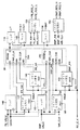
図11は、従来のカメラ一体型記録再生装置の概略構成ブロック図を示す。撮像素子110は、被写体の光学像を電気信号に変換し、その出力はA/D変換器112によりディジタル信号に変換されて撮影信号処理回路114に印加される。撮影信号処理回路114は、A/D変換器112からの画像データに色キャリア除去、アパーチャ補及びガンマ処理等を施して輝度成分信号を生成し、同時に、色補間、マトリクス変換、ガンマ処理及びゲイン調整等を施して色差成分信号を生成し、YUV等の形式の映像データをVRAM116に出力する。Yは輝度信号、Uは色差信号B−Y、Vは色差信号(R−Y)をそれぞれ示す。
【0003】
VRAM116は、例えば、ダイナミックRAM(DRAM)に書き込み用と読み出し用のポートを設けて水平ライン毎のアドレッシングを容易にしたビデオ表示専用のメモリ素子からなる。撮影信号処理回路114から出力されるYUV信号は、例えば、下記に示すような順序で、
(上位データ)Y0,Y1,Y2,Y3,Y4,Y5,・・・
(下位データ)U0,V0,U2,V2,U4,V4,・・・
画面片上から順にVRAM116に格納される。
【0004】
メモリ制御回路118は、画素拡大回路120により、VRAM116に記憶される画像データの一部を拡大してVRAM116に書き戻すことができる。メモリ制御回路118は、VRAM116の記憶データを順に読み出しTV系信号処理回路122に供給する。TV系信号処理回路122は、メモリ制御回路118からの画像データからコンポジット信号を生成してD/A変換器124に出力し、D/A変換器124は、TV系信号処理回路122のディジタルコンポジット信号をアナログ信号に変換する。LPF126はD/A変換器124の出力信号をビデオ信号の帯域に制限して、D/A変換結果に含まれる高周波ノイズを除去する。
【0005】
LPF126の出力は、ビデオアンプ128により増幅されてTVモニタ130に印加される。LPF126の出力はまた、液晶表示制御回路132に印加される。液晶表示制御回路132は、LPF126の出力からRGB信号を生成し、液晶表示パネル134を駆動して、液晶表示パネル34の画面上に画像を表示させる。液晶表示制御回路132には、NTSC用の場合で3.58MHzのサブキャリア用の水晶振動子が付属し、PAL用の場合では4.43MHzのサブキャリア用の水晶振動子が付属する。
【0006】
現在、ディジタルカメラ及びカムコーダに組み込まれる液晶表示パネルの多くは、フィールド画表示分のドット数(水平550×垂直220程度)しか具備しないので、インターレースのフレーム信号をそのまま印加すると、奇フィールドと偶フィールドが同一ライン上に表示され、画像がちらついてしまう。つまり、液晶表示パネルでは、一般的なTVモニタのようにインターライン方式でフレーム画を表示することができない。従って、液晶表示パネル上に画像を表示する場合、一般的には、フレーム画でなく、同一フィールドを2度印加することで、ちらつきの無い見やすい画像にしている。
【0007】
フレーム画からフィールド画に切り替える場合には、次のようにしていた。すなわち、VRAM116をフレームメモリで構成した場合、偶フィールドの各ラインに1フィールド前の奇フィールドの各ラインと同じデータを書き込む必要がある。そのために、フレーム画からフィールド画への切り替えには、1フィールド画を書き込むための時間が余分に必要になる。VRAM116を2個のフィールドメモリで構成した場合は、一方のフィールドのメモリ読み出しだけを毎フィールド行うことになり、フレーム画からフィールド画への切り替えを瞬時に行える。しかし、複数個のメモリ構成になるので、実装上の回路面積が大きくなる。
【0008】
表示画の一部を拡大表示する場合には、VRAM116の一部の画像データを画素拡大回路120で拡大して、再びVRAM116に書き戻す必要がある。更に、表示画の一部を他の画像と入れ替える場合には、別に第2のVRAMを用意して、第2のVRAMの一部の画像データを第1のVRAMに書き込む必要がある。
【0009】
【発明が解決しようとする課題】
従来例では、表示画像の一部を画像で代替する場合、代替途中の見苦しい画像を表示しないためには表示切り替え用の余計なVRAMが必要になり、DRAM容量が増大してしまうという問題があった。
【0010】
また、表示画像を部分的に拡大する場合には、処理途中の見苦しい画像を表示しないようにするために表示切り替え用の別のVRAMが必要になるだけでなく、画素拡大用回路で拡大しながら再びVRAMに書き戻す手順をとるので、拡大表示への切り替えに時間がかかるという問題があった。
【0011】
本発明は、このような問題点を解決する画像処理装置を提示することを目的とする。
【0012】
【課題を解決するための手段】
本発明に係る画像処理装置は、画像データを一時的に記憶する第1の記憶装置と、当該第1の記憶装置に画像データを書き込み及び読み出すインターフェース回路と、当該インターフェース回路により当該第1の記憶装置から読み出された画像データを一時記憶する第2の記憶装置と、当該画像データを表示する表示装置と、当該第1の記憶装置の読み出しアドレスを当該インターフェース回路に指示するアドレス発生回路であって、当該第1の記憶装置のビデオメモリ領域の指定部分を当該第1の記憶装置内の別の領域の記憶データで置換をするためのアドレスを発生自在なアドレス発生回路とを具備し、当該第2の記憶装置は当該表示装置の1画面分より少ない記憶容量を有しており、当該置換のために当該インターフェース回路により読み出された画像データを一時的に記憶し、記憶した順に当該画像データを読み出して当該表示装置へ出力し、当該表示装置において当該置換による画像データを水平方向に拡大して表示させる場合、当該第2の記憶装置による読み出しにより拡大率を制御し、当該表示装置において当該置換による画像データを垂直方向に拡大して表示させる場合、当該第1の記憶装置による読み出しにより拡大率を制御することを特徴とする。
【0013】
【実施例】
以下、図面を参照して、本発明の実施例を詳細に説明する。
【0014】
図1は、本発明の一実施例の概略構成ブロック図を示す。10は光学像を電気信号に変換する撮像素子、12は撮像素子10のアナログ出力をディジタル信号に変換するA/D変換器、14は、A/D変換器12の出力から、色キャリア除去、アパーチャ補正及びガンマ処理等により輝度データYを生成すると同時に、色補間、マトリクス変換、ガンマ処理及びゲイン調整等により色差データR−Y,B−Yを生成し、YUV形式のビデオデータを出力する撮影信号処理回路である。
【0015】
16は撮影画像データを一時記憶するDRAM(ダイナミック・ランダム・アクセス・メモリ)、18はDRAM16にデータを書き込む及び読み出すメモリ・インターフェースである。DRAM16上には、撮影画像(及び再生画像)をTVモニタ又は液晶表示パネルなどの画像表示装置で表示するためにその画像データを一時記憶するメモリ空間(VRAM)が割り当てられている。
【0016】
図2は、VRAMにおける画像データの格納形式例を示す。図2(1)はY:U:V=4:4:4の場合、同(2)はY:U:V=4:2:2の場合、同(3)はY:U:V=4:1:1の場合、同(4)はY:U:V=4:1:1で、再生の場合をそれぞれ示す。図2(2)のデータ量は、図2(1)の2/3であり、図32(3)のデータ量は図2(2)の3/4である。必要十分なデータ量が確保出来るように用途に応じてデータ形式を選択することで、メモリ容量及びデータ転送効率の最適化を図ることが出来る。これは、システム構成上、大変に有効である。本実施例では、DRAM16のVRAMには、Y:U:V=4:1:1形式で画像データを格納する。
【0017】
更にVRAMの構成条件として、VRAMサイズをNTSC方式では水平752画素×垂直494ライン分とし、PAL方式では水平736画素×垂直580ライン分とする。1フィールド分は、このライン数の半分に相当する容量になり、NTSC方式では247ライン分、PAL方式では290ライン分になる。
【0018】
従って、本実施例では、撮影信号処理回路14は、A/D変換器12からの撮影画像データを処理してY:U:V=4:2:2形式でメモリ・インターフェース18に出力し、メモリ・インターフェース18は、撮影信号処理回路14からのY:U:V=4:2:2形式の画像データをY:U:V=4:1:1形式に変換してDRAM16の自然画用VRAM領域に書き込む。
【0019】
20は、DRAM16の自然画用VRAMから画像データをダイレクト・メモリ・アクセス(DMA)方式で読み出す再生DMA制御回路である。22は、TVモニタ及び液晶表示パネルなどの画像表示装置の画面上に自然画にスーパーインポーズして表示する文字及びキャラクタ等のビットマップ(BMP)データをDRAM16からDMA方式で読み出すビットマップDMA制御回路である。
【0020】
再生DMA制御回路20は、TVモニタへ自然画のみを表示する場合に、VRAMデータを読み出すためのアドレスをメモリ・インターフェース18に出力し、メモリ・インターフェース18はこれに応じて、DRAM16から該当するアドレスの自然画データを読み出し、VALIDフラグといっしょにFIFO24に供給する。図3は、再生DMA制御回路20によるメモリ読み出しの模式図を示す。図3において、実線は奇フィールド、破線は偶フィールドのラインをそれぞれ示す。1,2,・・・,Nは、1フレーム内のライン番号を示す。通常、TVモニタはインターレース表示をしているので、これに合わせ、VRAMからの読み出しラインは1,3,5,・・・,N−1,2、,4,・・・,Nという順番になる。1フレームのライン数Nは、NTSCの場合に494本、PAL方式の場合に590本である。再生DMA制御回路20の設定により、データ読み出しをフレーム/フィールド表示及びNTSC方式/PAL方式に応じて変更できる。フィールド表示の時には、偶数ラインに対して、1ライン前の奇数ラインデータを読み出すことになる。
【0021】
再生DMA制御回路20と同様に、ビットマップDMA制御回路22もまた、その設定により、データ読み出しをフレーム/フィールド表示及びNTSC方式/PAL方式に応じて変更できる。
【0022】
24は、メモリ・インターフェース18からのデータを1/4ライン分、一時的に記憶するFIFO(ファーストイン・ファーストアウト)メモリである。26は1ラインの1/4の記憶容量を具備するSRAMである。FIFOメモリ24は、書き込みと読み出しで独立のポートを具備し、書き込み周期に対して非同期にデータを読み出すことが出来る。例えば、FIFOメモリ24の書き込み周期を、DRAM16のアクセスクロック周期、言い換えるとシステムクロックと同じ50MHzにする一方で、読み出しを、TV信号処理に適したサブキャリアの4倍クロック(4fsc=約14MHz)にする。これにより、TV信号処理のクロック周波数に依存せずに、システムクロック(DRAMクロック)を決定でき、システムのパフォーマンスを比較的自由に向上させることができる。FIFOメモリ24の出力は、図2(4)に示すY:U:V=4:1:1形式である。
【0023】
28は、Y:U:V=4:1:1形式をY:U:V=4:2:2形式に変換する変換回路である。ビデオ出力の帯域としては、Y:U:V=4:1:1の情報量で十分である。しかし、文字及びキャラクタ等のビットマップ画像は帯域が広く、これとスーパーインポーズするには、自然画データをY:U:V=4:2:2にしたほうが画質上、好ましい空である。
【0024】
30は、文字等のビットマップ画像データをパレットデータに変換するパレット変換回路である。ビットマップ画像データでそのままパレットの表示色を表現する場合、パレットの表示色の階調を多くすると1画素当たりのビット数が増え過ぎて、メモリ容量及びデータ転送効率を悪くしています。逆に1画素当たりのビット数を減らすと、パレットの表示色の階調が失われてしまう。そこで、ビットマップ画像データのビット幅をパレットの同時発色数に相当する値に設定し、パレット色の階調をある程度確保する方法を採用する。例えば、1画素当たりのビットマップ・データを4ビットとし、同時発色数を16にし、表示色の階調を16ビットで256階調にする。具体的には、16ビット幅のパレットレジスタを16個用意し、ビットマップデータの示す値によりこの16個のパレットレジスタから1つを選択する。つまり、1画面上の同時発色数はビットマップデータのビット幅によって決まり、パレット色の階調はパレットレジスタのビット幅によって決まる。従って、パレット色の階調を維持したまま、同時発色数を制限するだけで、ビットマップ領域のデータ容量を小さくすることができる。
【0025】
32は、変換回路28から出力される自然画像データに、パレット変換回路30から出力されるビットマップ画像データをスーパーインポーズする合成回路である。例えば、パレット色の階調の1つとして透明色を用意し、その透明色部分に自然画像データをはめ込む。これにより、ビットマップ画像と自然画像を画素毎に切り替えることが可能になる。更には、合成回路12の出力段にスーパーインポーズするか否かを選択自在なセレクタを設けることで、自然画像だけの出力と、ビットマップ画像を自然画像にスーパーインポーズした画像の出力を選択できるようになる。
【0026】
34は、合成回路32の出力にクロマエンコード処理、帯域補正及びコンポジット化等の表示用の処理を施す再生信号処理回路である。36は再生信号処理回路34の出力データをアナログ信号に変換するD/A変換器である。38は、FIFOメモリ24、SRAM26、変換回路28,30、合成回路32、再生信号処理回路及びD/A変換器36のそれぞれにタイミング信号を供給する同期信号発生器(SSG)である。
【0027】
本実施例の動作を説明する。撮像素子10の出力信号はA/D変換器12によりディジタル信号に変換されて撮影信号処理回路14に入力する。撮影信号処理回路14は入力画像データに、色キャリア除去、アパーチャ補正及びガンマ変換等の処理を施して輝度データYを生成し、色補間、マトリクス変換及びガンマ変換等の処理を施して色差データ色差データU(=B−Y),V(=R−Y)を生成する。撮影信号処理回路14の出力データは、図2(2)に示す形式で、画面左上から順に
(上位データ)Y0Y1Y2Y3Y4Y5Y6Y7・・・
(下位データ)U0V0U2V2U4V4U6V6・・・
とメモリ・インターフェース18に入力する。
【0028】
メモリ・インターフェース18は、撮影信号処理回路14からのデータを図2(3)に示す形式に変換し、
(上位データ)Y0Y1Y3Y4Y5Y7・・・
(下位データ)U0V0Y2V4U4Y6・・・
としてDRAM16の自然画VRAM領域に書き込む。
【0029】
TVモニタへ自然画のみを表示する場合における再生DMA制御回路20とメモリ・インターフェース18とのデータのハンドシェイクを説明する。同期信号発生器38が発生する同期タイミング信号は、垂直ブランキング中では、垂直同期(Vsync)時にFIFOメモリ24が空になりメモリ・インターフェース18への要求信号PB_REQ_L,PB_REQ_Hの両方をアクティブにする。この要求により、メモリ・インターフェース18は、再生DMA制御回路20で指示されたアドレス(自然画VRAM領域内)の画像データを読み出し、VALIDフラグと共にFIFOメモリ24に供給する。メモリ・インターフェース18は同時に、再生DMA制御回路20へのACK信号をアドレスを認識した合図としてアクティブにする。再生DMA制御回路20は、ACK信号がアクティブになったことを検知すると、次に読み出すべきデータのアドレスを計算し、メモリ・インターフェース18に出力する。
【0030】
この垂直ブランキング中には、FIFOメモリ24からデータが読み出されないので、次第にFIFOメモリ24にデータが充満し、要求信号PB_REQ_L,PB_REQ_Hはインアクティブ状態になる。FIFOメモリ24が空になると要求信号又はフラグPB_REQ_L,PB_REQ_Hは共にアクティブになる。FIFOメモリ24に1〜2割ほどデータが溜まると、信号PB_REQ_Hがインアクティブになるが、信号PB_REQ_Lはアクティブのままである。FIFOメモリ24に8割以上データが溜まると、信号PB_REQ_L,PB_REQ_Hは共にインアクティブになる。
【0031】
垂直ブランキングを抜けて映像期間に入ると、FIFOメモリ24からデータが読み出されていく。FIFOメモリ24のデータ量がFIOFOメモリ24のメモリ容量の8割を下回ると、前述したように信号PB_REQ_Lがアクティブになる。これに応じて、メモリ・インターフェース18が、VRAMデータを読み出してFIFOメモリ24へ転送する場合、信号PB_REQ_Hはインアクティブのままでも、次第にFIFOメモリ24にデータが満たされて、信号PB_REQ_Lがインアクティブになる。
【0032】
仮に、信号PB_REQ_Lがアクティブになっても、メモリ・インターフェース18がすぐに応答できない場合には、FIFOメモリ24のデータ残量が少なくなっていき、2割を下回った時点で、信号PB_REQ_Hがアクティブになる。メモリ・インターフェース18内では、信号PB_REQ_Hはプライオリティの高い要求として処理され、メモリ・インターフェース18は、即時にVRAMデータを読み出してFIFOメモリ24へ転送する。FIFOメモリ24にデータが溜まり、データ量が2割以上になると、信号PB_REQ_Hはインアクティブになる。更にFIFOメモリ24へのデータ書き込みが続き、データ量が8割を超えた時点で、信号PB_REQ_Lもインアクティブになる。信号PB_REQ_Hがインアクティブになった時点でFIFOメモリ24へのデータ書き込みが途絶えてしまうと、やがてデータ量が2割を下回った時点で、再び信号PB_REQ_Hがアクティブになる。信号PB_REQ_HがアクティブになってもVRAMデータがメモリ・インターフェース18から供給されない最悪の場合には、やがてFIFOメモリ24が空になる。FIFOメモリ24から読み出すデータが無くなると、TVモニタ上の表示も異常になる。従って、信号PB_REQ_Hのプライオリティを十分に高く設定し、このようなことが絶対に起きないようにしておく必要がある。
【0033】
本実施例では、DMA制御回路20は、クロックエッジのタイミングでACK信号を検出する。つまり、データの送受を連続的(バースト的)に行う場合は、前述のフラグ信号はアクティブになり続けて(アクティブハイの場合には、’H’のまま)、DRAM制御回路20は、クロックエッジのタイミングで連続的にACK信号を取り込む。従って、ACK信号がアクティブ状態のときには、DMA制御回路20は、1クロック毎にアドレス計算を実行して、アドレスをメモリ・インターフェース4へ出力する。ACK信号と同様に、VALID信号、PB_RWG_L信号及びPB_REQ_H信号等のフラグ信号も、連続的にアクティブになるので、クロックエッジのタイミングで連続的にデータが取り込まれる場合がありうる。当然ながら、単発時には1クロック幅のフラグ信号になる。
【0034】
映像期間中には、図2(4)に示すY:U:V=4:1:1形式でFIFOメモリ24からデータが読み出され、変換回路28に供給される。変換回路28は、前述したように、図2(4)に示すY:U:V=4:1:1形式の画像データを図2(2)に示すY:U:V=4:2:2形式に変換し、合成回路32に出力する。
【0035】
自然画のみを表示する場合、合成回路32は、単に、変換回路28の出力画像データをそのまま再生信号処理回路34に供給する。再生信号処理回路34は、合成回路32の出力にクロマエンコード処理、帯域補正及びコンポジット化等の信号処理を施してTV表示用映像データを生成し、D/A変換器36に出力する。D/A変換器36は再生信号処理回路34からの映像データをアナログ信号に変換して、図示しない画像表示装置に供給する。
【0036】
D/A変換器36以降の構成は、従来のカメラ一体型記録再生装置の構成と同じになるので、ここでは、説明を省略する。
【0037】
自然画像とビットマップ画像をスーパーインポーズして表示する場合の動作を説明する。
【0038】
自然画像データのDRAM16からの読み出しから変換回路28での変換までの処理は、上述の通りである。
【0039】
ビットマップ画像のDRAM16からの読み出しも、基本的に自然画像と同じである。即ち、垂直同期(Vsync)時にビットマップ用FIFOメモリ24は、空になり、メモリ・インターフェース18への要求信号BMP_REQ_L,BMP_REQ_Hの両方をアクティブにする。メモリ・インターフェース18は、ビットマップDMA制御回路22が示すDRAM16上のビットマップ・アドレスからデータを読み出し、ビットマップデータ用のVALIDフラグと共にFIFOメモリ24へ供給する。メモリ・インターフェース18は同時に、ビットマップDMA制御回路22へのBMP_ACK信号を、アドレスを認識した合図としてアクティブにする。ビットマップDMA制御回路22は、BMP_ACK信号がアクティブになったことを検知して、次に読み出すべきデータのアドレスを計算し、メモリ・インターフェース18に出力する。
【0040】
要求信号又はフラグBMP_REQ_L,BMP_REQ_Hの変化は、信号PB_REQ_L,PB_REQ_Hと同じである。すなわち、FIFOメモリ24が空になると、信号BMP_REQ_L,BMP_REQ_Hの両方がアクティブになる。FIFOメモリ24に1〜2割ほどデータが溜まると、信号BMP_REQ_Hのみがインアクティブになり、信号BMP_REQ_Lはアクティブのままである。FIFOメモリ24に8割以上データが溜まると、信号BMP_REQ_L,BMP_REQ_Hの両方がインアクティブになる。
【0041】
自然画像とビットマップ画像は、一般的に、TV及び液晶表示パネルなどの画像表示装置の画面上での表示領域又はサイズが異なり、本実施例では、ビットマップ画像の表示領域は水平640×垂直480であり、自然画像の表示領域より一回り小さい。そのため、ビットマップデータの読み出しタイミングも、自然画像データの読み出しタイミングの内側に位置し、転送に必要なFIFO容量も自然画より少ない。
【0042】
しかし、基本的な回路動作としては自然画像データのそれと同じでよい。すなわち、ビットマップデータの読み出しタイミングになると、FIFOメモリ24からビットマップデータが読み出されていき、FIFOメモリ24の残ビットマップデータ量がビットマップ用FIFOメモリ24の容量の8割を下回ると、信号BMP_REQ_Lがアクティブになる。この変化に対し、メモリ・インターフェース18がすぐに応答してビットマップデータをDRAM16から読み出してFIFOメモリ24へ送る場合、信号BMP_REQ_Hはインアクティブのままでも、次第にFIFOメモリ24にデータが満たされて、信号BMP_REQ_Lがインアクティブになっていく。
【0043】
仮に、信号BMP_REQ_Lがアクティブになったことにメモリ・インターフェース18がすぐに応答できない場合、FIFOメモリ24のデータ残量が少なくなっていき、2割を下回った時点で信号BMP_REQ_Hがアクティブになる。メモリ・インターフェース18内では、信号BMP_REQ_Hはプライオリティの高い要求として処理され、即時に、ビットマップデータをDRAM16から読み出してFIFOメモリ24へ送る。そして、次第にFIFOメモリ24にデータが溜まり、データ量が2割以上になると、信号BMP_REQ_Hはインアクティブになる。、更にFIFOメモリ24へのデータ書き込みが続き、データ量が8割を超えた時点で、信号BMP_REQ_Lもインアクティブになる。信号BMP_REQ_Hがインアクティブになった時点で、FIFOメモリ24へのデータ書き込みが途絶えると、やがてデータ量2割を下回った時点で、再び、信号BMP_REQ_Hがアクティブになる。
【0044】
上述の4つのデータリクエスト信号では、最も優先度の高いのがPB_REQ_H信号であり、以下、BMP_REQ_H信号、PB_REQ_L信号及びBMP_REQ_L信号と続く。従って、4つのデータリクエストが同時に発生した場合、メモリインターフェース18は、この優先順位に従ってデータを転送する。
【0045】
FIFOメモリ24から読み出されたビットマップデータは、パレット変換回路30に送られ、ここでパレットデータに変換される。パレット変換回路30のパレットデータ出力は合成回路32に送られる。合成回路32は、変換回路28からの自然画像データに変換回路30からのビットマップ画像データをスーパーインポーズする。合成回路32の出力は、再生信号処理回路34に送られる。再生信号処理回路34は、合成回路32の出力に、クロマエンコード処理、帯域補正及びコンポジット化等の信号処理を施してTV表示用映像データを生成し、D/A変換器36に出力する。D/A変換器36は再生信号処理回路34からの映像データをアナログ信号に変換して、図示しない画像表示装置に供給する。
【0046】
再生DMA制御回路20とビットマップDMA制御回路22のアドレス発生動作を説明する。図3は、フレーム構成のVRAMからのデータ読み出しの様子を示す。この場合、前述したように、奇フィールドに対して、奇数番目のライン#1,#3,#5,・・・,#(N−1)が順に読み出され、偶フィールドに対して偶数番目のライン#2,#4,・・・,#Nが順に読み出される。○印は、再生DMA制御回路20が発生する奇フィールドのスタートアドレスを示し、□印は、再生DMA制御回路20が発生する偶フィールドのスタートアドレスを示す。
【0047】
メモリ・インターフェース18がDRAM16から16ビットバス幅でインターフェースされているのであれば、再生DMA制御回路20が次に発生するアドレスは、上述のスタートアドレスに16ビット(2バイト)加算したアドレスになる。つまり、再生DMA制御回路20は、メモリ・インターフェース18からのACK信号がアクティブになると、現アドレスに16ビット(2バイト)加算しながらアドレス発生していく。
【0048】
メモリ・インターフェース18がDRAM16と32ビットバス幅でインターフェースしているときには、上述のスタートアドレスに32ビット(4バイト)加算したアドレスが、次に発生するアドレスになる。
【0049】
アドレスが2バイトづつ加算されながらラインの終りまでくると、次は、第3ラインの一番左の位置の画素データのアドレスになる。この場合の加算量は、2バイト+1ライン分(1128バイト)=1130バイトになる。この1130バイトは、奇フィールドがライン#1,#3,・・・,#(N−1)と1ライン置きにデータを読み出すことによるオフセット量(OFFA)である。
【0050】
奇フィールドのデータ(NTSC方式で、1128バイト×247ライン分)が全て読み出されると、再生DMA制御回路20は、図3に口印で示す偶フィールドのスタートアドレスを発生する。その後、奇フィールドのときと同様に、2バイトずつ加算したアドレスを発生し、ラインの終りではオフセット量の1130バイトを加算したアドレスを発生する。そして、偶フィールドのデータ(NTSC方式で、1128バイト×247ライン分)が全て読み出されると、再び、奇フィールドのスタートアドレスに戻り、以降、繰り返してVRAMのデータ読み出しが行われていく。
【0051】
再生DMA制御回路20は、NTSC規格とPAL規格のモード切り替えレジスタと、奇フィールドのスタートアドレスST_ADD_1を記憶するレジスタと、偶フィールドのスタートアドレスST_ADD_2を記憶するレジスタと、ライン終了から次のラインの先頭アドレスまでのオフセットOFFAを記憶するレジスタと、DRAM16のバス幅に応じた連続データの加算量を記憶するレジスタとを具備する。
【0052】
図4は、2つのフィールドメモリで構成したVRAMからのデータ読み出しの模式図を示す。図4(a)は、2つのフィールドメモリが隣接する場合、同(b)は2つのフィールドメモリが離れている場合をそれぞれ示す。図4(a)の場合、DRAM16上で、奇フィールドの最後の画素データに続いて、偶フィールドの初めの画素データが位置する。
【0053】
図4に示すメモリ構成の場合、奇フィールド及び偶フィールド内でライン・データが連続しているので、オフセット量が2バイト(DRAM16が32ビットバスは場のときには4バイト)になること、及び、偶フィールドのスタートアドレスが異なる点が、図3に示すメモリ構成の場合との相違点である。従って、この2点の設定変更を再生DMA制御回路20に設定することにより、図3に示すVRAM構成から図4に示すVRAM構成に容易に切り替えられる。図4に示す構成の場合、TVモニタ又は液晶表示パネルにフィールド表示するには、1つのフィールドメモリ分のデータで済むので、メモリ容量もフレーム構成の場合の半分で済むことになる。
【0054】
図4に示すVRAM構成を使用するのは、例えば、電子ビューファインダ(EVF)表示である。EVF表示では例えば、水平1600画素×垂直1200ラインの撮像素子から垂直画素同士を加算したフィールド(水平1600画素×垂直600ライン)を読み出し、縦横サイズを水平752画素×垂直247ラインにリサイズしてVRAMに書き込み、フィールド画を液晶表示パネルに表示する。
【0055】
この時、液晶表示パネルには、毎秒60フィールドを表示するが、撮像素子からは毎秒25乃至30フレームを読み出す。すなわち、VRAMの書き込みレートと読み出しレートが異なっている。単一のフィールドVRAMでは、図5に例示するように、走っている人の胴が切られているような大変見ずらい画像が表示される。図5では、破線を境に1フィールド(30m秒)分の時間差の画像が上下に表示される。すなわち、破線より下には前のフィールド画が表示され、破線より上に現在のフィールド画が表示される。
【0056】
本実施例では、VRAMを2つのフィールドメモリからなる構成とすることで、この不具合を生じないようにする。書き込み途中のフィールドメモリからはデータを表示用に読み出さずに、データ書き込みが完了した時点で表示用とする。そして、EVF動作から撮影動作に切り替えて、撮像素子からの画像をフレーム画としてVRAMにフリーズする場合、2枚のフィールドメモリの片方に奇フィールドを格納し、他方に偶フィールドを書き込み、奇フィールドのスタートアドレスにST_ADD_1を割り当て、偶フィールドのスタートアドレスにST_ADD_2を割り当てることにより、容易にフレーム画表示に切り替えることができる。
【0057】
本来、図3に示すVRAM構成も、図4に示すVRAM構成も1フレーム分のメモリ容量を必要とするが、図4に示すVRAM構成は、EVF動作などにおいて図3に示すVRAM構成より便利である。本実施例では、再生DMA制御回路20のレジスタ設定を変更することで、容易にどちらのVRAM構成にも対応できる。
【0058】
次に、表示画像の画素数よりも格段に多い画素数の撮像素子を使用し、その撮像素子の画素データを間引かずにVRAMに格納し、その一部を表示用に読み出す場合の動作を説明する。
【0059】
図6は、水平1600画素×垂直1200ラインのVRAMを構成し、その中の水平752画素×垂直494ラインの部分を表示用とする場合の模式図を示す。この場合、ラインの最後のデータと次のラインの最初のデータのアドレスは1600画素−752画素分、離れている。従って、図5に符号40で示す範囲内の画像を表示画とするためには、先に説明したオフセット量を、(巨大VRAMの1ライン)−(表示VRAMの1ライン)に設定する。これにより、巨大VRAMの一部の領域を表示できるようになる。
【0060】
図6においては、領域40,42は、画像表示する水平752画素×垂直494ラインの部分を示し、例えば、表示画像を領域40から領域42に移行する。これは単なるアドレス操作のみであり、簡単に行える。領域40の画像は、山頂にいる人物を示し、領域42の画像は、山頂からハングライダーで飛び降りている人物を示す。
【0061】
このように本実施例では、奇フィールド又は偶フィールドのスタートアドレスを変更するだけで、巨大VRAM中の任意の一部の画像を表示できる。一般的には、高画質な再生ズーム機能といえる。
【0062】
次に、図7を参照して、本実施例の置換機能を説明する。図7は、9面マルチ画表示の状態でその内の一枚を書き換える様子を示す模式図であって、マルチ画表示内の画像を更新する場合で、右上の画像を人物画から風景画に書き換えているところを示す。
【0063】
この置換機能は、再生DMA制御回路20内のアドレス発生回路に組み込まれる。このアドレス発生回路は、水平方向に1ライン分のカウンタと、垂直方向に表示ライン数分のカウンタを持ち、これらのカウンタを進めながら、前述したようにVRAMのアドレスを順次、発生する。すなわち、アドレス発生回路は、水平・垂直の各カウンタが図7に示す(DIS_XST,DIS_YST)から(DIS_XEND,DIS_YEND)で示された数値範囲内にある場合に、図7の右側の小さい枠領域の画像に対応するアドレスを発生する。図7の右側の小さい枠領域の画像は、アドレスST_SOR_ADD1又はST_SOR_ADD2を先頭に、アドレスST_SOR_ADD1又はST_SOR_ADD2から所定バイト(16ビットバス幅のとき2バイト、32ビットバス幅のとき4バイト)ずつ加算して隣接画素のアドレスを発せさせることで、表示用に読み出され得る。図7の右側の小さい枠の画像の水平方向右端までデータを読み出したら、VRAM上のメモリ領域に戻る。即ち、図7の右側の小さい枠のSOR_HSPAN分のデータを読み出したなら、VRAM上のメモリ領域に戻ることになる。
【0064】
VRAM上では、DIS_XSTにSOR_HSPAN分の値を加算したアドレスから順次、アドレスを発生させ、水平方向のカウンタが再びDIS_XST値乃至DIS_XEND値の領域内に入ったら、図7の右側の小さい枠領域の画像の第2ライン目のアドレスに切り替える。以降、水平・垂直のカウンタが(DIS_XST,DIS_YST)から(DIS_XEND,DIS_YEND)で示された領域内に入る度に、図7の右側の小さい枠領域の画像のアドレスが発生され、9面マルチ画表示の右上の画像が、図7の右側の小さい枠領域の画像で置換される。
【0065】
実際の利用に即して、この置換機能を説明する。先ず、撮影した画像のインデックス等を表示するのに、図7で示すようなマルチ画表示が行われる。この時、VRAM上に9枚の画像がマルチ画として書き込まれ、9面マルチ画として一括して画像表示される。9面マルチ画の右上の画像を更新する場合、例えば、図7上の右の別枠に示す人物画のように、9面マルチ画の右上の画像をVRAMとは別のメモリ領域にコピーする。そしてVRAM上の右上の画像を家の建ち並んだ風景画に書き換えるのであるが、このデータ書き換え中は、先に別のメモリ領域にコピーした人物画を上述の置換機能を用いて表示する。書き換えが終了した段階でこの部分置換を止めれば、表示画像は、更新された家の風景画を含む9面マルチ画に瞬時に切り替わる。すなわち、メモリデータを書き換える際の見苦しい画像をユーザに表示しないようにできる。
【0066】
従来は、マルチ画の書き換え途中の画像が表示されて、見苦しいものになっていた。または、これを避けるために、VRAMを別に設け、画像の書き換えが終ってからVRAMを切り替える等の処理を行っていた。しかし、この方法はVRAM容量が大幅に増加指定しまう。本実施例では、再生DMA制御回路20内に部分置換機能を設け、書き換えている部分に対しては、他のメモリ空間の画像を表示させることで、データ書き換え途中の見苦しい画像を表示しないようにしている。
【0067】
図8を参照して、本実施例の部分拡大機能を説明する。図8は、結婚式等の集合写真で、新郎新婦の部分を拡大表示した様子を示す。このような部分拡大機能は、被写体全体の画枠は決まっているが、被写体の一部を拡大して確認したい場合に用いられる。この部分拡大機能も、前述の置換機能と同様に、再生DMA制御回路20のアドレス発生回路に盛り込まれる。この時のアドレス発生は前述の置換機能の場合とほぼ同じである。異なる点として、表示エリアには、原画エリアの画像を拡大して表示していることである。換言すると、置換は、拡大率が等倍の部分拡大に相当する。例えば、図8では、水平垂直共に拡大率が2倍の部分拡大の場合を示しており、図8の(DIS_XST,DIS_YST)から(DIS_XEND,DIS_YEND)で示される拡大表示領域が、SOR_STアドレスから始まり、SOR_OFFSETとSOR_HSPANで規定される原画エリアの4倍になる。
【0068】
ここで垂直方向の拡大方法を説明する。回路としては、設定によって0から15までのライン繰り返しフラグを立てることのできる4ビットのバイナリカウンタを設け、このライン繰り返しフラグが立っている場合に、原画エリアのラインのアドレスを繰り返し発生させる。このように同一ラインデータを繰り返し表示することにより、垂直方向に等倍乃至16倍の拡大表示を行なえる。図8に例示した垂直方向の2倍拡大では、この4ビット・バイナリカウンタに1ライン置きにライン繰り返しフラグが立つように1を設定すればよい。
【0069】
水平方向の拡大は次のようにする。すなわち、FIFOメモリ24からデータを読み出すときに、画素繰り返しフラグが立っている場合に原画エリアの画素を繰り返し表示すればよい。画素繰り返しフラグ発生回路は、垂直の場合と多少異なり、整数倍率の2倍乃至16倍を切り替えられる4ビット・カウンタの他に、小数点倍率(1.1倍、1.2倍・・・など)を行うための4ビット・カウンタを設ける。従って、8ビットのレジスタ設定で等倍から16.9倍までを0.1倍単位で切り替えることができる。整数倍率は、(垂直方向と同様に)画素の繰り返しで拡大表示していき、例えば、1回繰り返しで2倍になり、2回繰り返しで3倍になる。
【0070】
小数点倍率について、図9及び図10を参照して説明する。図9は、1.x倍のときの小数点拡大時の繰り返しフラグ例を示し、図10は、9.x倍のときの小数点拡大時の繰り返しフラグ例を示す。図9に示す例では、0から9までの10画素中に繰り返しフラグを何回立てるかにより、小数点拡大倍率が決まる。例えば、図9に示すように、1.1倍時には10画素中に1回フラグをたて、1.2倍時には10画素中に2回、1.3倍時には10画素中に3回、1.4倍時には10画素中に4回、1.5倍時には10画素中に5回、1.6倍時には10画素中に6回、・・・、1.9倍時にはは10画素中に9回フラグを立てることになる。そして、フラグが立った画素が繰り返し表示される画素であり、拡大表示エリア全体でみるとあたかも小数点拡大されたように表示される。
【0071】
図10に示す9.x倍の例では、9.0倍時に10画素とも9回ずつフラグを立てているが、9.1倍時には10画素中の1画素に対し10回フラグをたて、残りの9画素に対して9回フラグを立てる。9.2倍時には、10画素中の2画素に対して10回フラグを立て、残りの8画素に対して9回をフラグを立てる。9.9倍時には、10画素中の9画素に対して10回フラグを立て、残りの1画素に対して9回フラグを立てる。つまり、繰り返す回数をとびとびに変更することにより、10画素単位でみたときに小数点の倍率で表示されるようにしている。
【0072】
図8に示す水平方向2倍拡大では、整数倍で1画素置きに繰り返しフラグが立つようにレジスタ設定する。これにより、垂直・水平の倍率が各2倍で、面積4倍の表示になる。
【0073】
原画エリアの画素が縦長の長方形の画素の場合、整数の高倍率表示を行なうと長方形の不自然な拡大表示になる。水平方向の小数点拡大は、これを回避するのに利用できる。
【0074】
図12は、ビットマップDMA制御回路22の内部構成を示す。50は水平方向のカウンタであり、XA_VALレジスタで設定される値を初期値としてダウンカウントする。水平方向カウンタ50は、入力のACKフラグに従いクロックCLKの立ち上がりに同期してダウンカウントする。リセット時及び次のラインの先頭(EN_0FF1=’1’)になると、初期値XA_VALがセットされる。カウンタ50の減少値ADDR_DELTAは、メモリ・インターフェース18からのデータ転送量によって異なり、例えば、DRAM16と32ビットバスで接続する場合には一回の転送が4バイトなので、4になる。
【0075】
52はEN_OFF1フラグ信号発生器であり、水平ライン方向カウンタ50の出力HTFRCをデコードして’0’になったとき、EN_OFF1フラグ信号を’1’にすることで、ラインの最終画素を示す。
【0076】
54は垂直方向カウンタであり、YA_VALレジスタで設定される値を初期値としてダウンカウントする。カウンタ54は、入力のACKフラグとEN_OFF1フラグに従い、クロックCLKの立ち上がりに同期してダウンカウントする。リセット時及び次のフィールドの先頭(EN_OFF12=’1’)になると、初期値YA_VALがセットされる。
【0077】
56はEN_OFF2フラグ信号発生器であり、垂直方向カウンタ54の出力VTFRCをデコードして’0’になったとき、EN_OFF2フラグ信号を’1’にすることで、フィールドの最終ラインを示す。
【0078】
58はアンド回路であり、EN_OFF1フラグ信号とEN_OFF2フラグ信号をアンドし、EN_OFF12フラグ信号を発生する。EN_OFF12フラグ信号は、フィールドの最終画素を示す。
【0079】
60はDRAM16上に構成されるビットマップ画像の読み出しアドレスを発生する読み出しアドレス発生回路である。読み出しアドレスアドレス回路60のEV_OD入力は同期信号発生38からの信号であり、奇フィールドか偶フィールドかを示す。DMA制御回路22がリセットされてRESET信号に’1’を入力したときに、読み出しアドレス発生回路60は、奇フィールドならば初期アドレスST_ADD_1から、偶フィールドならば初期アドレスST_ADD_2からそれぞれ読み出しアドレスを発生する。そして、回路60は、ACK入力に従いADDR_CNTをADDR_DELTA分ずつ増やして行く。ADDR_DELTAの値は、先に述べたように、メモリインターフェース18からのデータ転送量によって異なり、例えば、DRAM16と32ビットバスで接続する場合には一回の転送が4バイトなので、4になる。回路60の出力ADDR_CNTは、バイト単位でのアドレスになる。そして、EN_OFF1=’1’のとき水平方向の最後のアドレスを指定した後は、回路60は、OFFAレジスタ分加算して、次のラインの先頭アドレスに進む。
【0080】
図12に示す各回路の動作をVHDLで記述すると次のようになる。水平方向カウンタ50に対しては、

【0081】
EN_OFF1フラグ信号発生器52に対しては、
EN_OFF1<=’1’ WHEN(HTFRC=0) ELSE’0’;
である。
【0082】
垂直方向カウンタ54に対しては、
【0083】
EN_OFF2フラグ信号発生器56に対しては、
EN_0FF2<=’1’WHEN(VTFRC=0)ELSE’0’;
である。
【0084】
アンド回路58に対しては、
EN_OFF12<=EN_OFF1 AND EN_OFF2;
である。
【0085】
読み出しアドレス発生回路60に対しては、
【0086】
図13は、再生DMA制御回路20の概略構成ブロック図を示す。ビットマップDMA制御回路22に対して、前述の部分置換及び部分拡大を行なうための回路が付加されている。
【0087】
62は水平方向カウンタであり、XA_VALレジスタで設定される値を初期値としてダウンカウントする。水平方向カウンタ62は、入力のACKフラグに従いクロックCLKの立ち上がりに同期してダウンカウントして行く。リセット時及び次のラインの先頭(EN_OFF1=’1’)になると、初期値XA_VALがセットされる。カウンタ62の減少値ADDR_DELTAは、メモリインターフェース18からのデータ転送量によって異なり、例えば、DRAM16と32ビットバスで接続する場合には一個の転送が4バイトなので、4になる。
【0088】
64は、図8に示されるDIS_XSTの位置を示すEN_DIS_XSTフラグ信号を発生するデコーダである。デコーダ64は、水平方向カウンタ62の出力とレジスタDIS_XSTの値を比較して一致したときに、EN_DIS_XSTフラグ信号を’1’にする。
【0089】
66は、図8に示されるDIS_XENDの位置を示すEN_DIS_XENDフラグ信号を発生するデコーダである。デコーダ66は、レジスタDIS_XSTからレジスタSOR_HSPANを減算した値と水平方向カウンタ62の出力を比較して一致したときに、EN_DIS_XENDフラグ信号を’1’にする。
【0090】
68は、ラインの最終画素を示すEN_OFF1フラグ信号を発生するデコーダである。デコーダ68は、レジスタDIS_H_SPANとレジスタSOR_HSPANの差分値と水平方向カウンタ62の出力HTFRCとを比較して一致したときに、EN_○FF1フラグ信号を’1’にする。水平方向に部分拡大をしない場合には、この差分値は’0’になる。例えば2倍に拡大する場合は、レジスタDIS_H_SPANに対しレジスタSOR_HSPANの値が半分になる。
【0091】
70は垂直方向カウンタであり、YA_VALレジスタで設定される値を初期値としてダウンカウントする。垂直方向カウンタ70は、入力のACKフラグとEN_OFF1フラグに従い、クロックCLKの立ち上がりに同期してダウンカウントする。リセット時及び次のフィールドの先頭(EN_OFF12=’1’)になると、初期値YA_VALがセットされる。
【0092】
72はEN_OFF2フラグ信号発生用デコーダであり、垂直方向カウンタ54の出力VTFRCをデコードして’0’になったとき、EN_OFF2フラグ信号を’1’にすることで、フィールドの最終ラインを示す。
【0093】
74は、図8に示されるDIS_YSTの位置を示すEN_DIS_YSTフラグ信号を発生するデコーダである。デコーダ74は、水平方向カウンタ62の出力とレジスタDIS_YSTの値を比較して一致したときに、EN_DIS_YSTフラグ信号を’1’にする。
【0094】
76は、図8に示されるDIS_YENDの位置を示すEN_DIS_YENDフラグ信号を発生するデコーダである。デコーダ76は、レジスタDIS_YSTからレジスタSOR_HSPANを減算した値と水平方向のカウンタ62の出力を比較して一致したときに、EN_DIS_YENDフラグ信号を’1’にする。
【0095】
78はEN_OFF1フラグ信号とEN_OFF2フラグ信号をアンドするアンド回路である。アンド回路78の出力EN_OFF12フラグ信号は、フィールドの最終画素を示す。
【0096】
80は、DRAM16上に形成されるVRAMの読み出しアドレスを発生する読み出しアドレス発生回路である。アドレス発生回路80のEV_OD入力は、同期信号発生38からの信号であり、奇フィールドか偶フィールドかを示す。DMA制御回路20がリセットされてRESET信号に’1’を入力したときに、アドレス発生回路80は、奇フィールドならば初期アドレスST_ADD_1から、偶フィールドならば初期アドレスST_ADD_2からアドレスADDR_CNTを発生する。そして、回路80は、ACK入力に従いADDR_CNTをADDR_DELTA分ずつ増やして行く。ADDR_DELTAの値は、先に述べたようにメモリインターフェース18からのデータ転送量によって異なり、例えば、DRAM16と32ビットバスで接続する場合は1回の転送が4バイトなので、4になる。アドレス発生回路80の出力ADDR_CNTは、バイト単位でのアドレスになる。
【0097】
そして、EN_OFF1=’1’のとき水平方向の最後のアドレスを指定した後は、回路80は、OFFAレジスタ分加算して次のラインの先頭アドレスに進む。例えば、図3に示すような連続したフレーム画のVRAM構成の場合、1ライン分のアドレス量が加算される。また、図4に示すようなVRAM構成の場合、OFFAの値はADDR_DELTAと同じ値になる。
【0098】
更に、EN_OFF12=’1’のときのフィールド画の最終アドレスを指定した後は、アドレス発生回路80は、EV_ODフラグ信号をみて、奇フィールドならばST_ADD_1レジスタ値を設定し、偶フィールドならばST_ADD_2レジスタの値を設定する。従って、前述したように、液晶表示パネル又はTVモニタにフィールド画を表示したい場合には、ST_ADD_1の値とST_ADD_2の値を同じにすれば良い。ST_ADD_1ジスタとST_ADD_2レジスタの設定値を切り替えるだけで、フィールド画とフレーム画を瞬時に切り替えることが可能になる。
【0099】
82は、部分置換及び部分拡大の垂直方向のエリアを示すETS_ARIAフラグを発生する回路である。ETS_ARIAフラグは、図8に示すように、DIS_YSTの位置からDIS_YENDの位置までの垂直エリアを示す。
【0100】
84はEN_OFF1とACKをアンドするアンド回路であり、その出力は、ラインの終了ドレスのタイミングを示す。
【0101】
86は部分拡大時の垂直方向のライン繰り返しフラグETS_Y_REPを発生する回路である。回路86は、入力のETS_ARIA=’1’の期間のみ、動作する。EN_OFF1とACKのアンド信号のタイミングで判断する。例えば、垂直2倍拡大時には、レジスタINT_REP=’1’に設定することにより、1ラインおきにETSY_REPが’1’になる。3倍時には、レジスタINT_REP=’2’に設定することにより、2ライン間’1’で、1ライン’0’の3ラインを繰り返すことになる。
【0102】
88は、部分置換及び部分拡大時の原画像のアドレスを発生するアドレス発生回路である。回路88は、入力のETS_ARIA=’1’の期間のみ動作し、ラインの終了ドレスのタイミングでETS_Y_REPフラグが’1’になっているかどうかを判断して、アドレスを発生する。VRAMの読み出しアドレス発生回路80とは別に、回路88は、2つのスタートアドレスレジスタST_SOR_ADD1,ST_SOR_ADD2とライン間のオフセットレジスタSOR_OFFSETを具備し、原画アドレスETS_SOR_ADRを発生する。ここで発生したアドレスが、図7の部分置換及び図8の部分拡大の原画アドレスを示す。
【0103】
90は、ETS_AREAフラグとEN_DIS_XSTフラグをアンドするアンド回路であり、部分置換及び部分拡大の水平方向の開始タイミングを発生する。
【0104】
92はセレクタ、94はフリップフロップ(FF)である。回路90,92,94により、フリップフロップ94が、アンド回路90の力タイミングでADDR_CNT値をラッチすることにより、部分置換及び部分拡大する直前のアドレスを保持する。
【0105】
96は、フリップフロップ94で保持するアドレスとレジスタDIS_H_SPANを加算する加算器であり、部分置換及び部分拡大を終了した位置のアドレスDISP_END_ADRを算出して、アドレス発生回路80に供給する。読み出しアドレス発生回路80にETS_ARIA、ETS_SOR_ADR及びDISP_END_ADRを入力することで、部分置換及び部分拡大を実現する。
【0106】
ちなみに、水平拡大は、再生DMA制御回路では行なわずに、FIF024の内部で実現する。
【0107】
図13に示す各回路の動作をVHDLで記述すると次のようになる。水平方向のカウンタ62に対しては、
【0108】
EN_DIS_XSTフラグ信号発生用デコーダ64に対しては、
EN_DIS_XST<=”1”WHEN(HTFRC=DIS_XST_R
EG)ELSE’0’;
である。
【0109】
EN_DIS_XENDフラグ信号発生用デコーダ66に対しては、
ETS_XEND_CNT<=DIS_XST_REG−SOR_HSPAN;
EN_DIS_XEND<=’1’WHEN(HTFRC=ETS_XEND_CNT)ELSE’0’;
である。
【0110】
EN_OFF1フラグ信号発生用デコーダ68に対しては、
XA_SUB<=DIS_H_SPAN−SOR_HSPAN;
EN_OFF1<=’1’WHEN(HTFRC=XA_SUB)ELSE’0’;
である。
【0111】
垂直方向カウンタ70に対しては、
【0112】
EN_OFF2フラグ信号発生用デコーダ72に対しては、
EN_0FF2<=’1’WHEN(VTFRC=’0’)ELSE’0’;
である。
【0113】
EN_DIS_YSTフラグ信号発生用デコーダ74に対しては、
EN_DIS_YST<=’1’WHEN(VTFRC=DIS_YST_REG)ELSE’0’;
である。
【0114】
EN_DIS_YENDフラグ信号発生用デコーダ76に対しては、
EN_DIS_YEND<=’1’WHEN(VTFRC=DIS_YEND_REG)ELSE’0’;
である。
【0115】
アンド回路78に対しては、
EN_OFF12<=EN_OFF1 AND EN_OFF2;
である。
【0116】
読み出しアドレス発生回路80に対しては、
【0117】
ETS_ARIAフラグ発生回路82に対しては、
【0118】
アンド回路84に対しては、
LN_E_ACK<=(EN_OFF1 AND ACK);
である。
【0119】
ETS_Y_REP発生回路86に対しては、
【0120】
アドレス発生回路88に対しては、
【0121】
回路90,92,94からなるアドレス保持回路に対しては、
【0122】
加算器96に対しては、
DISP_END_ADR<=TEMP_XST_ADR+DIS_H_SPAN+ADDR_DELTA;
である。
【0123】
図14は、FIFO24の概略構成ブロック図を示す。SRAM26をアドレスで分ける事により、1つのSRAMで自然画とビットマップ画像の両用にしても良い。ここでは分かりやすくするために、自然画用とビットマップ用に別々にSRAMを使用する場合を説明する。従って、SRAM26aは、自然画FIFO用の2ポートSRAMであり、SRAM26bはビットマップFIFO用の2ポートSRAMを示す。SRAM26a,26bのDはデータ入力を、AWはライト側アドレスを、ARはリード側アドレスを、WR_CLKはライト側クロックを、RD_CLKはリード側クロックを、Qはデータ出力をそれぞれ示す。
【0124】
140は自然画入力データのラッチ回路であり、PB_VALID入力がアクティブのとき、WR_CLKの立ち上がりエッジでDATA入力をラッチする。
【0125】
142は、自然画用SRAM26aのライトアドレスを発生する回路であり、PB_VALID入力がアクティブになる度にWR_CLKの立ち上がりエッジに同期してライトアドレスPB_AWをインクリメントする。また、ライトアドレス発生回路142には、同期信号発生器38からの垂直同期信号VDがリセットとして入力され、フィールド画データの転送毎にアドレスがリセットされる。即ち、垂直同期信号VDによりPB_AWが初期化されてから、前述のVRAMのスタートアドレスのデータが転送され、SRAM26aの初期アドレスに書き込まれる。ライトアドレス発生回路142の内部で注意する点としては、同期信号発生器38からの垂直同期信号VDはRD_CLKのタイミングで発生しているので、WR_CLKとは非同期になる。そのため、回路142は、非同期信号の受け渡しを行なってWR_CLKに同期した垂直同期信号VDにタイミング切り替えをしている。
【0126】
144は自然画用SRAM26aのリードアドレスを発生する回路であり、TV信号の映像期間中に’1’になるNBLK信号が’1’のとき、RD_CLKの立ち上がりエッジに同期してリードアドレスPB_ARをインクリメントする。また、ライトアドレス発生回路142と同様に、回路144には、同期信号発生器38からの垂直同期信号VDがリセットとして入力され、フィールド画データの転送開始前にアドレスが初期化される。これにより、ライトアドレスPB_AWとの関係を一致させている。
【0127】
146はSRAM26aからの輝度出力を選択してデータを保持する輝度信号ラッチ回路である。SRAM26aからのデータ出力は図2(3)に示すようなY:U:V=4:1:1の構成になっており、3ckで4画素分のデータ出力になる。このSRAM26aの出力を図2(4)に示すようなデータ列にするために、4ck目はSRAM26aの読み出しを停止させて、輝度信号ラッチ回路146内に保持した輝度データY3を出力する。
【0128】
148はSRAM26aからの色差出力UVを選択してデータを保持する色差信号ラッチ回路である。SRAM26aからのデータ出力は図2の(3)に示すようなデータ列になっており、2ckで4画素分のデータ出力になる。このSRAM26aの出力を図2(4)に示すようなデータ列にするために、1ck目と2ck目のUVデータを保持して、1乃至2ck目はUを、3乃至4ck目はVを出力するようになっている。
【0129】
図13に示すDMA制御回路20で説明した水平方向拡大回路は、輝度信号ラッチ回路146と色差信号ラッチ回路148が水平方向拡大回路を構成する。これらの回路は、拡大開始と終了の画素位置を指定するレジスタと拡大倍率を指定するレジスタを持ち、拡大画素のタイミングに1画素前のデータを保持すること(前置補間)で水平方向の拡大を実現する。
【0130】
150は自然画用データリクエスト信号発生回路であり、前述した通りにFIF024のデータ残量を算出し、その残量に従ってリクエスト信号を発生する。残量を算出するために、ライトアドレス値BMP_AWからリードアドレス値BMP_ARを減算して得られる差値をデータ残量とする。注意する点として、WR_CLKの立ち上がりエッジに同期して演算を行なっている。リードアドレスBMP_ARはRD_CLKのタイミングで発生しているので、WR_CLKとは非同期になる。そのため、非同期信号の受け渡しを行なってWR_CLKに同期したBMP_ARにタイミングに切り替えている。
【0131】
152はビットマップ入力データのラッチ回路であり、入力のBMP_VALID信号がアクティブのとき、WR_CLKの立ち上がりエッジでDATA入力をラッチする。
【0132】
154はビットマップ用SRAM26bのライトアドレスを発生する回路であり、BMP_VALID入力がアクティブになる度に、WR_CLKの立ち上がりエッジに同期してBMP_AWをインクリメントする。回路154には、同期信号発生器38からの垂直同期信号VDがリセットとして入力され、フィールド画データの転送毎にアドレスがリセットされる。即ち、垂直同期信号VDでBMP_AWが初期化されてから、前述のVRAMのスタートアドレスのデータが転送され、SRAM26aの初期アドレスに書き込まれる。
【0133】
ライトアドレス発生回路154の内部で注意する点としては、同期信号発生器38からの垂直同期信号VDはRD_CLKのタイミングで発生しているので、WR_CLKとは非同期になる。そのため、非同期信号の受け渡しを行なってWR_CLKに同期した垂直同期信号VDにタイミング切り替えをしている。
【0134】
156はビットマップ用SRAM26bのリードアドレスを発生する回路であり、TV信号の映像期間中に’1’になるNBLK信号が’1’のとき、RD_CLKの立ち上がりエッジに同期してBMP_ARをインクリメントする。ライトアドレス発生回路142と同様に、同期信号発生器38からの垂直同期信号VDがリセットとして入力し、フィールド画データの転送開始前にアドレスが初期化されて、BMP_AWとの関係を一致させている。
【0135】
158はBMPデータラッチ回路である。SRAM26bのBMPデータ出力は1画素が4ビットデータの構成になっているので、下記のように1ckの16ビット中に4画素分のデータが転送される。即ち、
BMPのSRAM出力 1ck目 5ck目 9ck目
(上位8ビット) B2:B3 B6:B7 B10:B11
(下位8ビット) B0:B1 B4:B5 B8:B9
そのため、SRAM26bからのBMPデータを1ck目に保持して置き、次の2乃至4ck目まではSRAM26bからの読み出しを停止して、前に保持したデータを出力する。
【0136】
160はビットマップ用データリクエスト信号発生回路であり、前述した通りに、FIF024のデータ残量を算出して、その残量に従ってリクエスト信号を発生する。ここでは、残量を算出するために、ライトアドレス値BMP_AWからリードアドレス値BMP_ARを減算して得られる差値をデータ残量としている。WR_CLKの立ち上がりエッジに同期して演算を行なっていることに注意すべきである。リードアドレスBMP_ARはRD_CLKのタイミングで発生しているので、WR_CLKとは非同期になる。そのため、非同期信号の受け渡しを行なってWR_CLKに同期したBMP_ARにタイミング切り替えをしている。
【0137】
【発明の効果】
以上の説明から容易に理解できるように、本発明によれば、簡単な処理で表示画像の一部を代替できる。これにより、表示VRAMの一部を書き換える場合などにおいて、余計な書き換え用のVRAMエリアを持たずに書き換え途中の見苦しい表示を見せずに済み、VRAMを削減でき、従ってコストを低減できる。
【0138】
また、余計な拡大用VRAMを持たずに拡大表示への切り替えを瞬時で高品位に行なえるようになり、これにより、DRAMを削減でき、拡大画像表示切り替えが高品位に行なえる。
【図面の簡単な説明】
【図1】 本発明の一実施例の概略構成ブロック図である。
【図2】 画像データ形式の一覧である。
【図3】 フレーム構成のVRAMからのデータ読み出しの模式図である。
【図4】 フィールド構成のVRAMからのデータ読み出しの模式図である。
【図5】 単一VRAM構成で書き込みと読み出しのレートが異なる場合の不具合の表示例である。
【図6】 水平1600画素×垂直1200ラインの巨大VRAMを構成した場合のイメージ例を示す図である。
【図7】 9面マルチ画表示で部分置換機能を用いて右上画の書き換えを行なっているイメージ例を示す図である。
【図8】 部分拡大表示時のイメージ例を示す図である。
【図9】 1.x倍のときの小数点拡大時の繰り返しフラグ例である。
【図10】 9.x倍のときの小数点拡大時の繰り返しフラグ例である。
【図11】 従来例の概略構成ブロック図である。
【図12】 DMA制御回路22の概略構成ブロック図である。
【図13】 DMA制御回路20の概略構成ブロック図である。
【図14】 FIFO24及びSRAM26の概略構成ブロック図である。
【符号の説明】
10:撮像素子
12:A/D変換器
14:撮影信号処理回路
16:DRAM(ダイナミック・ランダム・アクセス・メモリ)
18:メモリ・インターフェース
20:再生DMA制御回路
22:ビットマップDMA制御回路
24:FIFO(ファーストイン・ファーストアウト)メモリ
26:SRAM
26a:自然画用SRAM
26b:ビットマップ用SRAM
28:411/422変換回路
30:パレット変換回路
32:合成回路
34:再生信号処理回路
36:D/A変換器
38:同期信号発生器(SSG)
50:水平方向カウンタ
52:EN_OFF1フラグ信号発生器
54:垂直方向カウンタ
56:EN_OFF2フラグ信号発生器
58:アンド回路
60: 読み出しアドレス発生回路
62:水平方向カウンタ
64:デコーダ
66:デコーダ
68:デコーダ
70:垂直方向カウンタ
72:デコーダ
74:デコーダ
76:デコーダ
78:アンド回路
80:読み出しアドレス発生回路
82:ETS_ARIAフラグ発生回路
84:アンド回路
86:ETS_Y_REP発生回路
88:アドレス発生回路
90:アンド回路
92:セレクタ
94:フリップフロップ(FF)
96:加算器
110:撮像素子
112:A/D変換器
114:撮影信号処理回路
116:VRAM
118:メモリ制御回路
120:画素拡大回路
122:TV系信号処理回路
124:D/A変換器
126:LPF
128:ビデオアンプ
130:TVモニタ
132:液晶表示制御回路
134:液晶表示パネル
140:ラッチ回路
142:ライトアドレス発生回路
144:リードアドレス発生回路
146:輝度信号ラッチ回路
148:色差信号ラッチ回路
150: 自然画用データリクエスト信号発生回路
152:ラッチ回路
154:ライトアドレス発生回路
156:リードアドレス発生回路
158:BMPデータラッチ回路
160: ビットマップ用データリクエスト信号発生回路[0001]
BACKGROUND OF THE INVENTION
The present invention relates to an image processing apparatus, and more specifically to an image processing apparatus used for video display.
[0002]
[Prior art]
FIG. 11 shows a schematic block diagram of a conventional camera-integrated recording / reproducing apparatus. The
[0003]
For example, the
(Upper data) Y 0 , Y 1 , Y 2 , Y 3 , Y 4 , Y 5 , ...
(Lower data) U 0 , V 0 , U 2 , V 2 , U 4 , V 4 , ...
They are stored in the
[0004]
The
[0005]
The output of the
[0006]
Currently, many liquid crystal display panels incorporated in digital cameras and camcorders have only the number of dots (horizontal 550 × vertical 220) for field image display, so when an interlaced frame signal is applied as it is, an odd field and even field Are displayed on the same line and the image flickers. That is, the liquid crystal display panel cannot display a frame image in an interline manner unlike a general TV monitor. Therefore, when an image is displayed on the liquid crystal display panel, in general, the same field is applied twice instead of the frame image to make the image easy to see without flicker.
[0007]
When switching from a frame image to a field image, the following was performed. That is, when the
[0008]
When a part of the display image is enlarged and displayed, it is necessary to enlarge a part of the image data in the
[0009]
[Problems to be solved by the invention]
In the conventional example, when a part of the display image is replaced with an image, an extra VRAM for switching the display is necessary in order not to display an unsightly image in the middle of the replacement, resulting in an increase in DRAM capacity. It was.
[0010]
Further, in the case of partially enlarging the display image, not only another display switching VRAM is required so as not to display an unsightly image in the middle of processing, but also a pixel enlarging circuit is enlarging. Since the procedure of writing back to the VRAM is taken again, there is a problem that it takes time to switch to the enlarged display.
[0011]
It is an object of the present invention to provide an image processing apparatus that solves such problems.
[0012]
[Means for Solving the Problems]
An image processing apparatus according to the present invention includes a first storage device that temporarily stores image data, an interface circuit that writes and reads image data to and from the first storage device, and the first storage device that uses the interface circuit. A second storage device that temporarily stores image data read from the device, a display device that displays the image data, and an address generation circuit that instructs the interface circuit to read out the address of the first storage device. An address generation circuit capable of generating an address for replacing the designated portion of the video memory area of the first storage device with the storage data of another area in the first storage device, The second storage device has a storage capacity smaller than one screen of the display device, and the interface circuit is used for the replacement. Temporarily storing image data Desa seen, outputs the stored in order reads the image data to the display device When the image data resulting from the replacement is enlarged and displayed on the display device in the horizontal direction, the enlargement ratio is controlled by reading out the second storage device, and the image data resulting from the replacement is displayed in the vertical direction on the display device. When displaying an enlarged image, the enlargement ratio is controlled by reading by the first storage device. It is characterized by doing.
[0013]
【Example】
Hereinafter, embodiments of the present invention will be described in detail with reference to the drawings.
[0014]
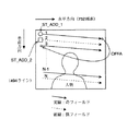
FIG. 1 shows a schematic block diagram of an embodiment of the present invention. 10 is an image sensor that converts an optical image into an electrical signal, 12 is an A / D converter that converts an analog output of the
[0015]
[0016]
FIG. 2 shows an example of a storage format of image data in the VRAM. 2 (1) shows the case of Y: U: V = 4: 4: 4, (2) shows the case of Y: U: V = 4: 2: 2, and (3) shows Y: U: V = In the case of 4: 1: 1, (4) shows Y: U: V = 4: 1: 1, and shows the case of reproduction. The data amount of FIG. 2 (2) is 2/3 of FIG. 2 (1), and the data amount of FIG. 32 (3) is 3/4 of FIG. 2 (2). By selecting the data format according to the application so that a necessary and sufficient amount of data can be secured, the memory capacity and the data transfer efficiency can be optimized. This is very effective in system configuration. In this embodiment, image data is stored in the VRAM of the
[0017]
Further, as VRAM configuration conditions, the VRAM size is set to 752 horizontal pixels × 494 vertical lines in the NTSC system, and 736 horizontal pixels × vertical 580 lines in the PAL system. One field has a capacity corresponding to half of the number of lines, which is 247 lines in the NTSC system and 290 lines in the PAL system.
[0018]
Therefore, in this embodiment, the photographic signal processing circuit 14 processes the photographic image data from the A / D converter 12 and outputs it to the
[0019]
A reproduction
[0020]
When displaying only a natural image on the TV monitor, the reproduction
[0021]
Similar to the reproduction
[0022]
A FIFO (first-in first-out)
[0023]
A
[0024]
A
[0025]
A
[0026]
A reproduction
[0027]
The operation of this embodiment will be described. The output signal of the
(Upper data) Y 0 Y 1 Y 2 Y 3 Y 4 Y 5 Y 6 Y 7 ...
(Lower level data) U 0 V 0 U 2 V 2 U 4 V 4 U 6 V 6 ...
To the
[0028]
The
(Upper data) Y 0 Y 1 Y 3 Y 4 Y 5 Y 7 ...
(Lower level data) U 0 V 0 Y 2 V 4 U 4 Y 6 ...
Is written in the natural image VRAM area of the
[0029]
A data handshake between the reproduction
[0030]
Since data is not read from the
[0031]
When the video period starts after passing through the vertical blanking, data is read from the
[0032]
If the
[0033]
In this embodiment, the
[0034]
During the video period, data is read from the
[0035]
When displaying only a natural image, the
[0036]
Since the configuration after the D /
[0037]
An operation when a natural image and a bitmap image are superimposed and displayed will be described.
[0038]
Processing from reading of natural image data from the
[0039]
Reading a bitmap image from the
[0040]
Changes in the request signals or flags BMP_REQ_L and BMP_REQ_H are the same as the signals PB_REQ_L and PB_REQ_H. That is, when the
[0041]
A natural image and a bitmap image generally have different display areas or sizes on the screen of an image display device such as a TV and a liquid crystal display panel. In this embodiment, the display area of a bitmap image is horizontal 640 × vertical. 480, which is slightly smaller than the natural image display area. For this reason, the read timing of bitmap data is located inside the read timing of natural image data, and the FIFO capacity required for transfer is less than that of natural images.
[0042]
However, the basic circuit operation may be the same as that of natural image data. That is, when the bitmap data read timing comes, the bitmap data is read from the
[0043]
If the
[0044]
Of the four data request signals described above, the PB_REQ_H signal has the highest priority, and follows the BMP_REQ_H signal, the PB_REQ_L signal, and the BMP_REQ_L signal. Accordingly, when four data requests occur simultaneously, the
[0045]
The bitmap data read from the
[0046]
The address generation operations of the reproduction
[0047]
If the
[0048]
When the
[0049]
When the address reaches the end of the line while adding 2 bytes at a time, the next is the address of the pixel data at the leftmost position of the third line. In this case, the addition amount is 2 bytes + 1 line (1128 bytes) = 1130 bytes. These 1130 bytes are an offset amount (OFFA) obtained by reading data every other line with the odd fields of
[0050]
When all the odd field data (1128 bytes × 247 lines in the NTSC system) is read, the reproduction
[0051]
The reproduction
[0052]
FIG. 4 is a schematic diagram of data reading from a VRAM configured with two field memories. FIG. 4A shows a case where two field memories are adjacent to each other, and FIG. 4B shows a case where two field memories are separated from each other. In the case of FIG. 4A, the first pixel data of the even field is located on the
[0053]
In the case of the memory configuration shown in FIG. 4, since the line data is continuous in the odd and even fields, the offset amount is 2 bytes (4 bytes when the
[0054]
The VRAM configuration shown in FIG. 4 is used, for example, for an electronic viewfinder (EVF) display. In the EVF display, for example, a field (horizontal 1600 pixels × vertical 600 lines) in which vertical pixels are added is read out from an image sensor of horizontal 1600 pixels × vertical 1200 lines, and the vertical and horizontal sizes are resized to horizontal 752 pixels × vertical 247 lines. The field image is displayed on the liquid crystal display panel.
[0055]
At this time, 60 fields per second are displayed on the liquid crystal display panel, but 25 to 30 frames per second are read from the image sensor. That is, the VRAM write rate and read rate are different. In the single field VRAM, as illustrated in FIG. 5, a very hard-to-see image in which the torso of a running person is cut is displayed. In FIG. 5, time difference images for one field (30 milliseconds) are displayed vertically above and below the broken line. That is, the previous field image is displayed below the broken line, and the current field image is displayed above the broken line.
[0056]
In this embodiment, the VRAM is configured by two field memories so that this problem does not occur. Data is not read from the field memory in the middle of writing for display, but is displayed when data writing is completed. When switching from the EVF operation to the shooting operation and freezing the image from the image sensor as a frame image in the VRAM, an odd field is stored in one of the two field memories, and an even field is written in the other. By assigning ST_ADD_1 to the start address and assigning ST_ADD_2 to the start address of the even field, it is possible to easily switch to frame image display.
[0057]
Originally, both the VRAM configuration shown in FIG. 3 and the VRAM configuration shown in FIG. 4 require a memory capacity of one frame, but the VRAM configuration shown in FIG. 4 is more convenient than the VRAM configuration shown in FIG. is there. In this embodiment, it is possible to easily cope with either VRAM configuration by changing the register setting of the reproduction
[0058]
Next, an operation is performed when an image sensor having a number of pixels significantly larger than the number of pixels of the display image is used, the pixel data of the image sensor is stored in the VRAM without being thinned, and a part thereof is read out for display. explain.
[0059]
FIG. 6 is a schematic diagram in the case where a VRAM of horizontal 1600 pixels × vertical 1200 lines is configured, and a portion of horizontal 752 pixels × vertical 494 lines therein is used for display. In this case, the address of the last data of the line and the first data of the next line is separated by 1600-752 pixels. Therefore, in order to set the image within the range indicated by
[0060]
In FIG. 6,
[0061]
As described above, in this embodiment, it is possible to display an arbitrary partial image in the huge VRAM only by changing the start address of the odd field or even field. In general, it can be said to be a high-quality playback zoom function.
[0062]
Next, the replacement function of this embodiment will be described with reference to FIG. FIG. 7 is a schematic diagram showing a state in which one of them is rewritten in the state of nine-screen multi-image display. Ah Thus, when updating the image in the multi-image display, the upper right image is rewritten from a portrait image to a landscape image.
[0063]
This replacement function is incorporated in an address generation circuit in the reproduction
[0064]
On the VRAM, addresses are generated sequentially from the address obtained by adding the value of SOR_HSPAN to DIS_XST, and when the horizontal counter enters the DIS_XST value to DIS_XEND value area again, the image in the small frame area on the right side of FIG. Switch to the second line address. Thereafter, each time the horizontal / vertical counter enters the area indicated by (DIS_XEND, DIS_YEND) from (DIS_XST, DIS_YST), the address of the image in the small frame area on the right side of FIG. The image in the upper right of the display is replaced with the image in the small frame area on the right in FIG.
[0065]
This replacement function will be described according to actual use. First, multi-image display as shown in FIG. 7 is performed in order to display the index of the photographed image. At this time, nine images are written as multi-images on the VRAM, and the images are collectively displayed as nine-screen multi-images. When updating the upper right image of the nine-screen multi-image, for example, the upper-right image of the nine-screen multi-image is copied to a memory area different from the VRAM, like a person image shown in the right separate frame in FIG. The upper right image on the VRAM is rewritten to a landscape image in which houses are arranged. During this data rewriting, the person image previously copied to another memory area is displayed using the above-described replacement function. If this partial replacement is stopped when the rewriting is completed, the display image is instantaneously switched to a nine-screen multi-image including the updated landscape image of the house. That is, an unsightly image when rewriting memory data can be prevented from being displayed to the user.
[0066]
Conventionally, an image in the middle of rewriting a multi-image is displayed, which is unsightly. Alternatively, in order to avoid this, a VRAM is provided separately, and processing such as switching the VRAM after image rewriting is completed. However, this method designates that the VRAM capacity is greatly increased. In this embodiment, a partial replacement function is provided in the reproduction
[0067]
With reference to FIG. 8, the partial enlargement function of a present Example is demonstrated. FIG. 8 shows an enlarged view of the bride and groom part in a group photo of a wedding or the like. Such a partial enlargement function is used when an image frame of the entire subject is determined but it is desired to enlarge and confirm a part of the subject. This partial enlargement function is also incorporated in the address generation circuit of the reproduction
[0068]
Here, an enlargement method in the vertical direction will be described. As a circuit, a 4-bit binary counter capable of setting a line repeat flag from 0 to 15 by setting is provided. When this line repeat flag is set, the address of the line in the original image area is repeatedly generated. By repeatedly displaying the same line data in this way, it is possible to perform an enlarged display of the same magnification or 16 times in the vertical direction. In the double enlargement in the vertical direction illustrated in FIG. 8, it is only necessary to set 1 so that the line repeat flag is set every other line in the 4-bit binary counter.
[0069]
The horizontal expansion is as follows. That is, when data is read from the
[0070]
The decimal point magnification will be described with reference to FIGS. FIG. FIG. 10 shows an example of a repetitive flag when the decimal point is enlarged at x times. An example of a repetition flag at the time of enlarging the decimal point when x times is shown. In the example shown in FIG. 9, the decimal point enlargement magnification is determined by how many times the repetitive flag is set in 10 pixels from 0 to 9. For example, as shown in FIG. 9, a flag is set once in 10 pixels at 1.1 times, twice in 10 pixels at 1.2 times, and 3 times in 10 pixels at 1.3 times. 4 times in 10 pixels at 4 times, 5 times in 10 pixels at 1.5 times, 6 times in 10 pixels at 1.6 times, ... 9 in 10 pixels at 1.9 times Times will be flagged. A pixel with a flag is a pixel that is repeatedly displayed, and is displayed as if the decimal point is enlarged when viewed in the entire enlarged display area.
[0071]
9. As shown in FIG. In the x-fold example, all 10 pixels are flagged 9 times at 9.0 times, but at 9.1 times, one pixel in 10 pixels is flagged 10 times and the remaining 9 pixels are flagged. Flag up 9 times. At 9.2 times, a flag is set 10 times for 2 pixels out of 10 pixels, and a flag is set 9 times for the remaining 8 pixels. At 9.9 times, the flag is set 10 times for 9 pixels out of 10 pixels, and the flag is set 9 times for the remaining one pixel. In other words, the number of repetitions is changed rapidly so that it is displayed at the decimal scale when viewed in units of 10 pixels.
[0072]
In the double enlargement in the horizontal direction shown in FIG. 8, the register is set so that a flag is repeatedly set every other pixel at an integer multiple. As a result, the vertical / horizontal magnification is doubled and the area is quadrupled.
[0073]
When the pixels in the original image area are vertically long rectangular pixels, an unnatural enlarged display of a rectangle is obtained when high-magnification display of integers is performed. Horizontal decimal expansion can be used to avoid this.
[0074]
FIG. 12 shows the internal configuration of the bitmap
[0075]
[0076]
[0077]
[0078]
An AND
[0079]
[0080]
The operation of each circuit shown in FIG. 12 is described in VHDL as follows. For the
[0081]
For the EN_OFF1
EN_OFF1 <= '1' WHEN (HTFRC = 0) ELSE '0';
It is.
[0082]
For the
[0083]
For the EN_OFF2
EN_0FF2 <= '1'WHEN (VTFRC = 0) ELSE' 0 ';
It is.
[0084]
For the AND
EN_OFF12 <= EN_OFF1 AND EN_OFF2;
It is.
[0085]
For the read
[0086]
FIG. 13 shows a schematic block diagram of the reproduction
[0087]
[0088]
A
[0089]
A
[0090]
A
[0091]
Reference numeral 70 denotes a vertical counter, which counts down using the value set in the YA_VAL register as an initial value. The vertical counter 70 counts down in synchronization with the rising edge of the clock CLK in accordance with the input ACK flag and EN_OFF1 flag. At the time of resetting and at the beginning of the next field (EN_OFF12 = '1'), the initial value YA_VAL is set.
[0092]
[0093]
A
[0094]
A
[0095]
An AND
[0096]
[0097]
Then, after specifying the last address in the horizontal direction when EN_OFF1 = '1', the
[0098]
Further, after designating the final address of the field image when EN_OFF12 = '1', the
[0099]
A circuit 82 generates an ETS_ARIA flag indicating a vertical area for partial replacement and partial enlargement. As shown in FIG. 8, the ETS_ARIA flag indicates a vertical area from the position of DIS_YST to the position of DIS_YEND.
[0100]
An AND
[0101]
A
[0102]
[0103]
[0104]
[0105]
[0106]
Incidentally, horizontal enlargement is realized within the FIF 024 without being performed by the reproduction DMA control circuit.
[0107]
The operation of each circuit shown in FIG. 13 is described in VHDL as follows. For the
[0108]
For the EN_DIS_XST flag
EN_DIS_XST <= “1” WHEN (HTFRC = DIS_XST_R
EG) ELSE '0';
It is.
[0109]
For the EN_DIS_XEND flag
ETS_XEND_CNT <= DIS_XST_REG-SOR_HSPAN;
EN_DIS_XEND <= '1'WHEN (HTFRC = ETS_XEND_CNT) ELSE' 0 ';
It is.
[0110]
For the EN_OFF1 flag
XA_SUB <= DIS_H_SPAN-SOR_HSPAN;
EN_OFF1 <= '1'WHEN (HTFRC = XA_SUB) ELSE' 0 ';
It is.
[0111]
For the vertical counter 70,
[0112]
For the EN_OFF2 flag
EN — 0FF2 <= “1” WHEN (VTFRC = “0”) ELSE “0”;
It is.
[0113]
For the EN_DIS_YST flag
EN_DIS_YST <= '1'WHEN (VTFRC = DIS_YST_REG) ELSE' 0 ';
It is.
[0114]
For the EN_DIS_YEND flag
EN_DIS_YEND <= '1'WHEN (VTFRC = DIS_YEND_REG) ELSE'0';
It is.
[0115]
For the AND
EN_OFF12 <= EN_OFF1 AND EN_OFF2;
It is.
[0116]
For the read
[0117]
For the ETS_ARIA flag generator 82,
[0118]
For the AND
LN_E_ACK <= (EN_OFF1 AND ACK);
It is.
[0119]
For the
[0120]
For the
[0121]
For the address holding circuit comprising the
[0122]
For the
DISP_END_ADR <= TEMP_XST_ADR + DIS_H_SPAN + ADDR_DELTA;
It is.
[0123]
FIG. 14 shows a schematic block diagram of the
[0124]
A natural image input data latch
[0125]
A
[0126]
144 is a circuit for generating the read address of the
[0127]
A luminance
[0128]
[0129]
In the horizontal direction enlargement circuit described in the
[0130]
A natural image data request
[0131]
A bitmap input data latch
[0132]
A
[0133]
As a point to be noted inside the write
[0134]
A
[0135]
BMP SRAM output 1st 5th 5th 9th
(
(
Therefore, the BMP data from the
[0136]
A bitmap data request
[0137]
【The invention's effect】
As can be easily understood from the above description, according to the present invention, a part of the display image can be replaced with a simple process. As a result, when a part of the display VRAM is rewritten, it is not necessary to display an unsightly display in the middle of rewriting without having an extra VRAM area for rewriting, and the VRAM can be reduced, thus reducing the cost.
[0138]
Further, it becomes possible to instantaneously switch to an enlarged display without having an extra VRAM for enlarging, so that the DRAM can be reduced, and an enlarged image display can be switched to a high quality.
[Brief description of the drawings]
FIG. 1 is a schematic block diagram of an embodiment of the present invention.
FIG. 2 is a list of image data formats.
FIG. 3 is a schematic diagram of data reading from a frame-structured VRAM.
FIG. 4 is a schematic diagram of data reading from a VRAM having a field configuration.
FIG. 5 is a display example of a defect when the writing and reading rates are different in a single VRAM configuration.
FIG. 6 is a diagram showing an example of an image when a huge VRAM of horizontal 1600 pixels × vertical 1200 lines is configured.
FIG. 7 is a diagram illustrating an image example in which the upper right image is rewritten using the partial replacement function in the nine-screen multi-image display.
FIG. 8 is a diagram illustrating an example of an image at the time of partial enlargement display.
FIG. 9 It is an example of a repetitive flag at the time of enlargement of the decimal point when x times.
FIG. It is an example of a repetitive flag at the time of enlargement of the decimal point when x times.
FIG. 11 is a schematic block diagram of a conventional example.
12 is a block diagram of a schematic configuration of a
13 is a block diagram of a schematic configuration of a
14 is a schematic block diagram of the
[Explanation of symbols]
10: Image sensor
12: A / D converter
14: Shooting signal processing circuit
16: DRAM (dynamic random access memory)
18: Memory interface
20: Reproduction DMA control circuit
22: Bitmap DMA control circuit
24: FIFO (first-in first-out) memory
26: SRAM
26a: SRAM for natural images
26b: SRAM for bitmap
28: 411/422 conversion circuit
30: Pallet conversion circuit
32: Synthesis circuit
34: Reproduction signal processing circuit
36: D / A converter
38: Synchronization signal generator (SSG)
50: Horizontal counter
52: EN_OFF1 flag signal generator
54: Vertical counter
56: EN_OFF2 flag signal generator
58: AND circuit
60: Read address generation circuit
62: Horizontal counter
64: Decoder
66: Decoder
68: Decoder
70: Vertical counter
72: Decoder
74: Decoder
76: Decoder
78: AND circuit
80: Read address generation circuit
82: ETS_ARIA flag generation circuit
84: AND circuit
86: ETS_Y_REP generation circuit
88: Address generation circuit
90: AND circuit
92: Selector
94: flip-flop (FF)
96: Adder
110: Image sensor
112: A / D converter
114: Shooting signal processing circuit
116: VRAM
118: Memory control circuit
120: Pixel enlargement circuit
122: TV system signal processing circuit
124: D / A converter
126: LPF
128: Video amplifier
130: TV monitor
132: Liquid crystal display control circuit
134: Liquid crystal display panel
140: Latch circuit
142: Write address generation circuit
144: Read address generation circuit
146: Luminance signal latch circuit
148: Color difference signal latch circuit
150: Natural image data request signal generation circuit
152: Latch circuit
154: Write address generation circuit
156: Read address generation circuit
158: BMP data latch circuit
160: Bitmap data request signal generation circuit
Claims (3)
当該第1の記憶装置に画像データを書き込み及び読み出すインターフェース回路と、
当該インターフェース回路により当該第1の記憶装置から読み出された画像データを一時記憶する第2の記憶装置と、
当該画像データを表示する表示装置と、
当該第1の記憶装置の読み出しアドレスを当該インターフェース回路に指示するアドレス発生回路であって、当該第1の記憶装置のビデオメモリ領域の指定部分を当該第1の記憶装置内の別の領域の記憶データで置換をするためのアドレスを発生自在なアドレス発生回路
とを具備し、
当該第2の記憶装置は当該表示装置の1画面分より少ない記憶容量を有しており、当該置換のために当該インターフェース回路により読み出された画像データを一時的に記憶し、記憶した順に当該画像データを読み出して当該表示装置へ出力し、当該表示装置において当該置換による画像データを水平方向に拡大して表示させる場合、当該第2の記憶装置による読み出しにより拡大率を制御し、当該表示装置において当該置換による画像データを垂直方向に拡大して表示させる場合、当該第1の記憶装置による読み出しにより拡大率を制御することを特徴とする画像処理装置。A first storage device for temporarily storing image data;
An interface circuit for writing and reading image data to and from the first storage device;
A second storage device for temporarily storing image data read from the first storage device by the interface circuit;
A display device for displaying the image data;
An address generation circuit for instructing the interface circuit of a read address of the first storage device, wherein a designated portion of a video memory area of the first storage device is stored in another area in the first storage device An address generation circuit capable of generating an address for replacement with data;
The second storage device has a storage capacity smaller than one screen of the display device, temporarily stores the image data read by the interface circuit for the replacement, and stores the image data in the order of storage. When the image data is read out and output to the display device, and the image data obtained by the replacement is enlarged and displayed in the horizontal direction on the display device, the enlargement ratio is controlled by reading out from the second storage device, In the image processing apparatus, when the image data obtained by the replacement is enlarged and displayed in the vertical direction, the enlargement ratio is controlled by reading by the first storage device.
Priority Applications (1)
| Application Number | Priority Date | Filing Date | Title |
|---|---|---|---|
| JP23798399A JP4280368B2 (en) | 1999-08-25 | 1999-08-25 | Image processing device |
Applications Claiming Priority (1)
| Application Number | Priority Date | Filing Date | Title |
|---|---|---|---|
| JP23798399A JP4280368B2 (en) | 1999-08-25 | 1999-08-25 | Image processing device |
Publications (3)
| Publication Number | Publication Date |
|---|---|
| JP2001069449A JP2001069449A (en) | 2001-03-16 |
| JP2001069449A5 JP2001069449A5 (en) | 2006-09-21 |
| JP4280368B2 true JP4280368B2 (en) | 2009-06-17 |
Family
ID=17023385
Family Applications (1)
| Application Number | Title | Priority Date | Filing Date |
|---|---|---|---|
| JP23798399A Expired - Fee Related JP4280368B2 (en) | 1999-08-25 | 1999-08-25 | Image processing device |
Country Status (1)
| Country | Link |
|---|---|
| JP (1) | JP4280368B2 (en) |
Families Citing this family (3)
| Publication number | Priority date | Publication date | Assignee | Title |
|---|---|---|---|---|
| US7304675B2 (en) * | 2003-06-10 | 2007-12-04 | Raytheon Company | Digital timing rate buffering for thermal stability of uncooled detectors |
| JP4578197B2 (en) * | 2004-09-29 | 2010-11-10 | 三洋電機株式会社 | Image display device |
| JP4470930B2 (en) | 2006-09-21 | 2010-06-02 | ソニー株式会社 | Image processing apparatus, image processing method, and program |
-
1999
- 1999-08-25 JP JP23798399A patent/JP4280368B2/en not_active Expired - Fee Related
Also Published As
| Publication number | Publication date |
|---|---|
| JP2001069449A (en) | 2001-03-16 |
Similar Documents
| Publication | Publication Date | Title |
|---|---|---|
| JP3562049B2 (en) | Video display method and apparatus | |
| JP4312238B2 (en) | Image conversion apparatus and image conversion method | |
| US8508610B2 (en) | Video signal processing apparatus | |
| JP2652401B2 (en) | Time-expanded video signal generator | |
| JP2005326684A (en) | Video device and imaging device | |
| JP2000284776A (en) | Picture processor | |
| JP4263190B2 (en) | Video composition circuit | |
| JP3801242B2 (en) | Reduced image display device | |
| JP2003069960A (en) | Video processor for realizing panorama/water glass function and its realization method | |
| EP0862322B1 (en) | Digital camera | |
| US7336302B2 (en) | Frame memory device and method with subsampling and read-out of stored signals at lower resolution than that of received image signals | |
| JP4280368B2 (en) | Image processing device | |
| JPH11289551A (en) | Display device and its control method | |
| JP3178665B2 (en) | Image size conversion method and device therefor | |
| US8531350B2 (en) | Display control apparatus, and setting method and program for display control apparatus | |
| JP3268999B2 (en) | Video signal processing circuit | |
| JP2001069448A (en) | Image processor | |
| JP4717168B2 (en) | Signal processing apparatus and signal processing method | |
| JP4089590B2 (en) | Video display method | |
| JP3855988B2 (en) | Video display method | |
| JP2000115694A (en) | Image data recording method and device thereof, image data reproducing method and device thereof information recording medium and computer-readable recording medium | |
| JP4261666B2 (en) | Image processing device | |
| JP3562050B2 (en) | Video processing method and computer system | |
| JPH07181937A (en) | Image processor | |
| JPH0431892A (en) | Video signal displaying device |
Legal Events
| Date | Code | Title | Description |
|---|---|---|---|
| A521 | Request for written amendment filed |
Free format text: JAPANESE INTERMEDIATE CODE: A523 Effective date: 20060808 |
|
| A621 | Written request for application examination |
Free format text: JAPANESE INTERMEDIATE CODE: A621 Effective date: 20060808 |
|
| A131 | Notification of reasons for refusal |
Free format text: JAPANESE INTERMEDIATE CODE: A131 Effective date: 20080219 |
|
| A521 | Request for written amendment filed |
Free format text: JAPANESE INTERMEDIATE CODE: A523 Effective date: 20080410 |
|
| A131 | Notification of reasons for refusal |
Free format text: JAPANESE INTERMEDIATE CODE: A131 Effective date: 20081202 |
|
| A521 | Request for written amendment filed |
Free format text: JAPANESE INTERMEDIATE CODE: A523 Effective date: 20090120 |
|
| TRDD | Decision of grant or rejection written | ||
| A01 | Written decision to grant a patent or to grant a registration (utility model) |
Free format text: JAPANESE INTERMEDIATE CODE: A01 Effective date: 20090303 |
|
| A01 | Written decision to grant a patent or to grant a registration (utility model) |
Free format text: JAPANESE INTERMEDIATE CODE: A01 |
|
| A61 | First payment of annual fees (during grant procedure) |
Free format text: JAPANESE INTERMEDIATE CODE: A61 Effective date: 20090316 |
|
| FPAY | Renewal fee payment (event date is renewal date of database) |
Free format text: PAYMENT UNTIL: 20120319 Year of fee payment: 3 |
|
| R150 | Certificate of patent or registration of utility model |
Free format text: JAPANESE INTERMEDIATE CODE: R150 |
|
| FPAY | Renewal fee payment (event date is renewal date of database) |
Free format text: PAYMENT UNTIL: 20130319 Year of fee payment: 4 |
|
| FPAY | Renewal fee payment (event date is renewal date of database) |
Free format text: PAYMENT UNTIL: 20140319 Year of fee payment: 5 |
|
| LAPS | Cancellation because of no payment of annual fees |