JP4277339B2 - Active pixel sensor readout channel - Google Patents
Active pixel sensor readout channel Download PDFInfo
- Publication number
- JP4277339B2 JP4277339B2 JP01641899A JP1641899A JP4277339B2 JP 4277339 B2 JP4277339 B2 JP 4277339B2 JP 01641899 A JP01641899 A JP 01641899A JP 1641899 A JP1641899 A JP 1641899A JP 4277339 B2 JP4277339 B2 JP 4277339B2
- Authority
- JP
- Japan
- Prior art keywords
- voltage
- output
- active pixel
- signal
- capacitor
- Prior art date
- Legal status (The legal status is an assumption and is not a legal conclusion. Google has not performed a legal analysis and makes no representation as to the accuracy of the status listed.)
- Expired - Lifetime
Links
Images


Classifications
-
- H—ELECTRICITY
- H03—ELECTRONIC CIRCUITRY
- H03F—AMPLIFIERS
- H03F3/00—Amplifiers with only discharge tubes or only semiconductor devices as amplifying elements
- H03F3/04—Amplifiers with only discharge tubes or only semiconductor devices as amplifying elements with semiconductor devices only
- H03F3/08—Amplifiers with only discharge tubes or only semiconductor devices as amplifying elements with semiconductor devices only controlled by light
- H03F3/082—Amplifiers with only discharge tubes or only semiconductor devices as amplifying elements with semiconductor devices only controlled by light with FET's
-
- H—ELECTRICITY
- H04—ELECTRIC COMMUNICATION TECHNIQUE
- H04N—PICTORIAL COMMUNICATION, e.g. TELEVISION
- H04N25/00—Circuitry of solid-state image sensors [SSIS]; Control thereof
- H04N25/60—Noise processing, e.g. detecting, correcting, reducing or removing noise
- H04N25/616—Noise processing, e.g. detecting, correcting, reducing or removing noise involving a correlated sampling function, e.g. correlated double sampling [CDS] or triple sampling
-
- H—ELECTRICITY
- H04—ELECTRIC COMMUNICATION TECHNIQUE
- H04N—PICTORIAL COMMUNICATION, e.g. TELEVISION
- H04N25/00—Circuitry of solid-state image sensors [SSIS]; Control thereof
- H04N25/60—Noise processing, e.g. detecting, correcting, reducing or removing noise
- H04N25/67—Noise processing, e.g. detecting, correcting, reducing or removing noise applied to fixed-pattern noise, e.g. non-uniformity of response
- H04N25/671—Noise processing, e.g. detecting, correcting, reducing or removing noise applied to fixed-pattern noise, e.g. non-uniformity of response for non-uniformity detection or correction
- H04N25/677—Noise processing, e.g. detecting, correcting, reducing or removing noise applied to fixed-pattern noise, e.g. non-uniformity of response for non-uniformity detection or correction for reducing the column or line fixed pattern noise
-
- H—ELECTRICITY
- H04—ELECTRIC COMMUNICATION TECHNIQUE
- H04N—PICTORIAL COMMUNICATION, e.g. TELEVISION
- H04N25/00—Circuitry of solid-state image sensors [SSIS]; Control thereof
- H04N25/70—SSIS architectures; Circuits associated therewith
- H04N25/76—Addressed sensors, e.g. MOS or CMOS sensors
- H04N25/77—Pixel circuitry, e.g. memories, A/D converters, pixel amplifiers, shared circuits or shared components
-
- H—ELECTRICITY
- H04—ELECTRIC COMMUNICATION TECHNIQUE
- H04N—PICTORIAL COMMUNICATION, e.g. TELEVISION
- H04N25/00—Circuitry of solid-state image sensors [SSIS]; Control thereof
- H04N25/70—SSIS architectures; Circuits associated therewith
- H04N25/76—Addressed sensors, e.g. MOS or CMOS sensors
- H04N25/78—Readout circuits for addressed sensors, e.g. output amplifiers or A/D converters
Landscapes
- Engineering & Computer Science (AREA)
- Multimedia (AREA)
- Signal Processing (AREA)
- Power Engineering (AREA)
- Transforming Light Signals Into Electric Signals (AREA)
- Solid State Image Pick-Up Elements (AREA)
Description
【0001】
【発明の属する技術分野】
この発明は、一般にアナログのアクティブ画素センサの読み出しチャネルに関し、より具体的には、電流モード利得補助のアクティブ画素センサのための差動入力シングルエンドのアナログ読み出しチャネルに関する。
【0002】
【従来の技術】
電子カメラは、一般に光学画像を一組の電子信号に変換する。電子信号は、カメラで受け取られた光の色の強度を表すことができる。通常、電子カメラは、画像センサまたは光検出器の配列を備え、カメラで受け取られた光の強度を検出する。典型的に、画像センサは電子信号を生成し、この電子信号は、センサによって受け取られた光の強度に比例する振幅を持つ。電子信号は、画像処理ができるよう、調整およびサンプリングされることができる。
【0003】
信号処理回路をもつ画像センサの集積化が、撮像システムの小形化および改良を可能にするので、より重要になってきている。アナログおよびデジタル信号処理回路と画像センサの集積化により、電子カメラ・システムは、低コストかつコンパクトであり、低電力であることが可能になる。
【0004】
歴史的に、画像センサは、主として電荷結合素子(CCD)である。CCDは比較的小さく、高いフィルファクター(fill factor)を提供することができる。しかし、CCDは、デジタルおよびアナログ回路と集積化するのが非常に難しい。さらに、CCDは、大量の電力を消費し、画像のスメアー(smear)という問題に苦しんでいる。
【0005】
歴史的に、CCDは、ソリッドステート(solid-state;固体)可視光撮像デバイスの用途で典型的に使用される光電性の画素セルである。しかし、光電性の画素セル内に信号増幅回路を持つフォトゲートまたはフォトダイオードを備えるCMOSのアクティブ画素センサは、CCDに対するいくつかの利点を提供する。CMOSのアクティブ画素センサ(active pixel sensor)は、より少ない電力を消費し、よりコストがかからないで製造することができ、より低い電源電圧を必要とし、大規模集積回路に集積するのがCCDよりも簡単である。さらに、CMOSのアクティブ画素センサを、低コストで大量の特定用途向けIC(ASIC)プロセスで製造することができる。したがって、ASIC製造業者は、光電性の画素セルを開発することができる。CMOS技術が進むにつれ、ASICの製造業者は、さらに製造コストを低減させることができ、さらなる性能の利益を提供することができる。
【0006】
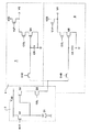
図1は、従来技術の光電性の画素セル2および対応する読み出しチャネル4を示す。読み出しチャネル4は、光画像信号の出力VSおよび基準出力VRを含む。
【0007】
画素セル2は、画素セル2によって受け取られる光の強度に比例した振幅を持つ出力信号を生成する。しかし、出力信号は、雑音の固定パターンをも含む。雑音の固定パターンは、画素セルによって受け取られる光の強度および出力信号の結果としての振幅の間の対応関係を減少させる。さらに、プロセス、温度およびバイアスの多様性のために、雑音の固定パターンは、異なる画素セル間で変化する。
【0008】
画素セル2は、フォトダイオードD1、リセット・トランジスタQ1および出力トランジスタQ2、Q3を備える。一般に、画素セル2の固定パターン雑音は、フォトダイオードD1の暗電流雑音および散弾雑音、リセット・トランジスタQ1のリセットおよびクロック雑音、および出力トランジスタQ2の利得の変動から成る。前に言及したように、プロセス、温度および画素セル間におけるバイアス状況の違いのため、雑音固定パターンは、異なる画素セル間で変化する。
【0009】
光電性の画素セルの配列の光電性の画素セルのそれぞれにより蓄積される電荷をサンプリングすることにより、電子画像が取り込まれる。それぞれの光電性の画素セルによって蓄積された電荷の量は、光電性の画素セルの光電部分によって受け取られる光の強度に比例する。光電性の画素セルの固定雑音パターンは、光電性の画素セルによって伝導された電荷のサンプリングされた値、および光電性の画素セルにより受け取られた光の強度の間の相関関係を減少させる。
【0010】
画素セル2が光に全くさらされない間に、画素セル2の応答をサンプリングすることによって、画素セル2の固定パターン雑音の基準応答を判断することができる。取り込まれた画像から基準応答を減算することにより、画素セル2の配列の固定パターン雑音のために取り込まれた電子画像におけるエラーを除去することができる。このプロセス(相関ダブル・サンプリング(correlated double sampling)と呼ばれる)は、従来技術の光電性の画素セル2および対応する読み出しチャネル4により、信号応答を生成する光画像信号出力VSをサンプリングし、かつ、基準応答を生成する基準出力VRをサンプリングすることで、達成される。したがって、画素セルの配列のそれぞれの画素セル2について、サンプリングされた電子画像内の固定パターン雑音の影響を除去するのに、2つのサンプルが必要とされる。大きい配列では、多数の電子サンプルが、画像を構成するのに必要とされる。
【0011】
読み出しチャネル4は、信号増幅回路6および基準増幅回路8を備える。信号増幅回路6および基準増幅回路8は、オフセット・エラーを含む。オフセット・エラーは、画素セル2の応答およびサンプリングされた電子画像の間の対応関係を減少させる。信号増幅回路および基準増幅回路への入力を、あらかじめ決められた電位に駆動することによって、および信号出力VSの電位およびサンプリングされたオフセット電圧を生成する基準出力VRをサンプリングすることにより、オフセット・エラーを見積もることができる。信号応答および基準応答から、サンプリングされたオフセット電圧を減ずることによって、取り込まれた画像からオフセット・エラーを除去することができる。しかし、これは、電子応答を取り込むのに、画素の配列内のそれぞれの画素について4つのサンプルを必要とする。
【0012】
画素セルの配列内のそれぞれの画素セル2は、光画像信号の出力VSおよび基準出力VRを持つ読み出しチャネル4を備える。多くの読み出しチャネルの信号出力VSおよび基準出力VRは、典型的に、「ビット線(bitline)」と呼ばれる導電線に接続される。一般に、多くの出力が1つのビット線に接続される。ビット線は、信号出力VSおよび基準出力VRにとって容量性の負荷になる。信号出力VSおよび基準出力VRが画素セル2の信号電圧または基準電圧を表す電位にビット線を駆動するのに必要なセトリング時間(セトリングタイム)が、容量性負荷によって増える。また、修正時間は、読み出しチャネルの電流駆動の能力に依存する。図1に示される読み出しチャネル4は、限られた電流駆動を提供する。したがって、ビット線に関連する容量が充電されるにつれ、従来技術の読み出しチャネル4の出力をサンプリングするのに、過大な修正時間を必要とすることがある。
【0013】
図1で示される読み出しチャネル4は、画素セル2の出力信号および信号出力VSの間に、約0.5から0.9の利得係数を提供する。したがって、画素セル2の出力信号は、読み出しチャネル4の出力でサンプリングされる前に、大いに減衰される。この減衰は、画素セル2の出力信号のSN比を減少させる。
【0014】
【発明が解決しようとする課題】
CMOSの画素セルの配列の応答をサンプリングすることにより作られる電子的にサンプリングされた画像に関連する固定パターン雑音を除去するアクティブ画素センサを持つことが望ましい。理想的には、アクティブ画素センサの読み出しチャネルは、電子的にサンプリングされた画像を取り込むのに必要なサンプル数を最小にする。さらに、標準CMOSプロセスを使用して製造された光画素セルの配列を用いて、アクティブ画素センサの読み出しチャネルを動作させることができる。現在の読み出しチャネルより大きい電流駆動を提供するアクティブ画素センサの読み出しチャネルを持ち、容量性ビット線に接続されるチャネル出力のセトリング時間を改善することが望ましい。さらに、1より大きいアクティブ画素センサの利得係数を持つことが望ましい。
【0015】
【課題を解決するための手段】
本発明は、CMOSの製造プロセスと互換性のあるアクティブ画素センサの読み出しチャネルを提供する。アクティブ画素センサは、単一差動出力、拡大されたダイナミックレンジ、改善された電流利得、改善された電流駆動およびアクティブ画素センサの読み出しチャネルに接続されたバス相互接続線の低減された容量性負荷を提供する。単一差動出力は、電子画像を構成するのに使用されるべきアクティブ画素センサの読み出しチャネルの配列に必要なサンプル数を減らす。改善された電流駆動は、アクティブ画素センサの読み出しチャネルの出力で生成される電位のセトリング時間を減らす。
【0016】
本発明の第1の実施形態は、アクティブ画素センサの読み出しチャネルを備える。アクティブ画素センサの読み出しチャネルは、アクティブ画素を備える。アクティブ画素は、アクティブ画素により受け取られた光の強度に比例した振幅を持つ信号電圧に、アクティブ画素の出力を駆動する。アクティブ画素は、アクティブ画素が光を受け取っていない時には、アクティブ画素の出力を基準電圧に駆動する。さらに、アクティブ画素センサの読み出しチャネルは、サンプルアンドホールド(sample and hold)回路を備え、アクティブ画素の出力を受け取る。サンプルアンドホールド回路は、信号電圧をサンプリングして格納し、基準電圧をサンプリングして格納する。サンプルアンドホールド回路は、格納された信号電圧の出力と、格納された基準電圧の出力とを等しく(等化)して、等化された出力電圧を提供する等化器回路を含む。さらに、アクティブ画素センサの読み出しチャネルは、サンプリングされて格納された信号電圧およびサンプリングされて格納された基準電圧の間の差から第1の差電圧を生成し、また、等化された出力電圧から第2の差電圧を生成する緩衝増幅器を備える。さらに、複数のバス相互接続線も備えており、緩衝増幅器のオフセットエラーを補正するために、第1のバス相互接続線が第1の差電圧を受け取り、かつ、第2のバス相互接続線が第2の差電圧を受け取るよう、緩衝増幅器の出力に選択的に接続される。
【0017】
本発明の第2の実施形態は、第1の実施形態に類似している。第2の実施形態の緩衝増幅器は、サンプリングして格納された信号電圧およびサンプリングして格納された基準電圧を受け取る差動入力シングルエンド増幅段を備える。差動入力シングルエンド増幅段は、サンプリングして格納された信号電圧およびサンプリングして格納された基準電圧の間の差に比例した電位を含む1つの出力電圧を生成する。さらに緩衝増幅器は、この1つの出力電圧を受け取り、1つの出力電圧の電位に比例した振幅を持つ緩衝器電流を生成する緩衝段を備える。さらに緩衝増幅器は利得段を備え、これは、緩衝器電流を受け取り、差電圧を生成し、および緩衝器電流の振幅より大きい振幅を持つよう予め調整された出力電流を生成する。
【0018】
本発明の第3の実施形態は、第1の実施形態に類似する。第3の実施形態のサンプルアンドホールド回路は、信号コンデンサおよび信号電圧スイッチを備え、アクティブ画素の出力を信号コンデンサに接続し、信号コンデンサが信号電圧を格納できるようにする。サンプルアンドホールド回路はさらに、基準コンデンサおよび基準電圧スイッチを備え、アクティブ画素の出力を基準コンデンサに接続し、基準コンデンサが基準電圧を格納できるようにする。
【0019】
本発明の第4の実施形態は、第3の実施形態に類似する。第4の実施形態は、信号コンデンサおよび基準コンデンサを放電する回路を備える。
【0020】
本発明の他の側面および利点は、本発明の原理の例として示し、図と共に得られる以下の詳細な記述により明らかになるであろう。
【0021】
【発明の実施の形態】
明瞭にするため図に示されるように、本発明は、アクティブ画素センサの読み出しチャネルに具体化される。アクティブ画素センサの読み出しチャネルは、単一差動出力、拡大されたダイナミックレンジ、改善された電流利得、改善された電流駆動およびアクティブ画素センサの読み出しチャネルに接続されるバス相互接続線の低減された容量性負荷を備える。単一差動出力は、電子画像を構成するのに使用されるべきアクティブ画素センサの読み出しチャネルの配列に必要なサンプル数を減らす。改善された電流駆動は、アクティブ画素センサの読み出しチャネルの出力で生成される電位のセトリング時間を減らす。
【0022】
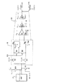
図2は、本発明の第1の実施形態を示し、この実施形態は、アクティブ画素センサの読み出しチャネルを備える。アクティブ画素センサの読み出しチャネルは、アクティブ画素2、サンプルアンドホールド回路10および緩衝増幅器20を備える。アクティブ画素2は、アクティブ画素出力において電圧(VAP)を生成し、これは、アクティブ画素2により受け取られる光の強度に比例した振幅を持つ。サンプルアンドホールド回路10は、アクティブ画素2の出力に接続される。サンプルアンドホールド回路10は、アクティブ画素2により受け取られた光の強度に比例した振幅を持つ信号電圧をサンプリングして格納する。さらに、サンプルアンドホールド回路10は、アクティブ画素2により生成された固定雑音パターンに比例した振幅を持つ基準電圧をサンプリングして格納する。緩衝増幅器20は、サンプリングして格納された信号電圧およびサンプリングして格納された基準電圧の間の差電圧を生成する。緩衝増幅器のこの差電圧は、アクティブ画素2の固定雑音パターンが、アクティブ画素2の信号電圧から内部的に減算された1つの出力電圧である。従来技術と異なり、固定雑音パターンは、アクティブ画素の出力電圧がサンプリングされる前に、信号電圧から減算される。したがって、本発明は、従来技術に比べ、電子画像を生成するのに半分の数のサンプル数を必要とする。
【0023】
図2は、1つのアクティブ画素2を示す。しかし、典型的には、光画像を電子的にサンプリングする目的で、多くのアクティブ画素2が配列に組み合わされ、その配列により光画像が検出される。
【0024】
図3は、本発明の他の実施形態を示す。この実施形態は、より詳細なサンプルアンドホールド回路10を備える。サンプルアンドホールド回路10は、信号コンデンサCS、基準コンデンサCR、信号スイッチトランジスタQ2、基準スイッチトランジスタQ3および対の等化器トランジスタQ4、Q5を備える。
【0025】
信号スイッチトランジスタQ2は、アクティブ画素2が光にさらされている時に「オン」にされる。アクティブ画素が光にさらされている時のアクティブ画素2により生成される信号電圧は、信号コンデンサCSに格納される。基準スイッチトランジスタQ3は、アクティブ画素2が光にさらされていない時に「オン」にされる。アクティブ画素2が光にさらされていない時のアクティブ画素2により生成される基準電圧は、基準コンデンサCRに格納される。信号コンデンサCSに格納される信号電圧VSは、緩衝増幅器20への第1の入力である。基準コンデンサCRに格納される基準電圧VRは、緩衝増幅器20への第2の入力である。
【0026】
緩衝増幅器20は、信号電圧VSの電位および基準電圧VRの電位の間の差に比例した差電圧を生成する。しかし、緩衝増幅器20は、合計して緩衝増幅器20の出力になる内部のオフセット電圧に悩まされる。緩衝増幅器の第1の入力および第2の入力を予め決められた電圧に駆動し、対応する緩衝器(バッファ)のオフセット電圧をサンプリングすることにより、オフセット電圧を判断することができる。第1および第2の入力は、信号コンデンサCSおよび基準コンデンサCRを共通の電圧に充電することにより、予め決められた電圧に駆動される。EQ制御線は、等化器(イコライザ)トランジスタQ4、Q5を「オン」にし、これらのトランジスタは、信号コンデンサCSおよび基準コンデンサCRを、電位VBASEにまで充電する。信号コンデンサCSおよび基準コンデンサCRが共通の電位VBASEにまで充電される時に、緩衝器のオフセット電圧がサンプリングされる。緩衝器のオフセット電圧のサンプルは、次の信号サンプルから減算され、緩衝増幅器20に関連するオフセット電圧エラーを除去する。
【0027】
出力トランジスタQ11、Q13は、アクティブ画素センサの読み出しチャネルの2つの別々の出力OUT1、OUT2を提供する。第1の制御線SHD1の電位が正にパルスされて、第1の出力トランジスタQ11をオンにし、このトランジスタは、緩衝増幅器20の差電圧を、第1の出力OUT1につなげる。第1の制御線は、緩衝増幅器20の差電圧がサンプリングされるべき時に、正にパルスされる。第2の制御線SHD2の電位が正にパルスされて、第2の出力トランジスタQ13をオンにし、このトランジスタは、緩衝増幅器20の緩衝器オフセット電圧を、第2の出力OUT2につなげる。第2の制御線は、緩衝増幅器20の緩衝器オフセット電圧がサンプリングされるべき時に、正にパルスされる。
【0028】
図3は、放電トランジスタQ1を示す。放電トランジスタQ1は、信号スイッチトランジスタQ2または基準スイッチトランジスタQ3が導通している間の、PRE_DSCH制御線が高電位にパルスする時に、信号コンデンサCSまたは基準コンデンサCRのどちらかについて放電の経路を与える。一般に、信号コンデンサCSおよび基準コンデンサCRは、信号電圧または基準電圧がサンプリングされて格納される前に、放電される。信号コンデンサCSおよび基準コンデンサCRを放電することにより、信号コンデンサCSおよび基準コンデンサCRに格納された電位をリセットする。これは、信号電圧および基準電圧が、より正確に格納されることを可能にする。さらに、信号コンデンサCSおよび基準コンデンサCRを放電することは、信号電圧および基準電圧のセトリング時間を減らす。
【0029】
バイアストランジスタQ10は、アクティブ画素2の出力についてバイアス電圧を与える。典型的に、アクティブ画素2は、アクティブ画素2の出力が固定電圧にバイアスされる時に、より良く機能するソースホロワー回路を備える。
【0030】
緩衝増幅器20は、差電圧および出力電流を生成し、ここで差電圧の振幅および出力電流の振幅は、信号電圧VSおよび基準電圧VRの間の電位差に比例する。従来技術の緩衝器は、1より小さい利得(典型的には0.9)を含む。本発明の緩衝増幅器20の利得は、1より大きい利得(典型的には約1.5)を含む。1より大きい、アクティブ画素センサの緩衝増幅器20の利得の増加は、1より小さい利得を含む従来技術の緩衝増幅器に比べ、より良い信号の保全性を提供する。アクティブ画素センサの緩衝増幅器20の利得は、差動入力電圧の信号および雑音のレベルを増加させる。アクティブ画素センサの緩衝増幅器20の出力に結びつく雑音源の影響は、それほど大きくない。したがって、出力信号の全体のSN比が改善される。
【0031】
緩衝増幅器20は、3段備える。差動入力シングルエンド(DTS)変換段22、緩衝またはソースホロワー段24および電流モード利得段26である。
【0032】
図4は、本発明の他の実施形態を示す。この実施形態は、より詳細な緩衝増幅器20内の回路を備える。
【0033】
DTS変換段22は、信号電圧VSおよび基準電圧VRを受け取り、単一のDTS差動電圧V DTS を生成する。この単一のDTS差動電圧V DTS は、信号電圧VSの電位および基準電圧VRの電位の間の差に比例した振幅を持つ。DTS変換段22は、入力トランジスタMP1、MP2および出力トランジスタMP3、MP4を備える。
【0034】
緩衝またはソースホロワー段24は、単一のDTS差動電圧V DTS の電圧振幅に比例した出力電流を生成する。ソースホロワー段24は、緩衝(buffering)および電圧から電流への変換を提供する。ソースホロワー段24は、入力トランジスタMN1およびソースホロワー・トランジスタMN2を備える。ソースホロワー・トランジスタMN2は、ダイオード接続される。すなわち、ソースホロワー・トランジスタMN2のソースは、ソースホロワー・トランジスタMN2のベースに電気的に接続される。ソースホロワー・トランジスタMN2がダイオード接続されるので、電圧から電流への変換が生じる。
【0035】
電流モード利得段26は、さらなる電流利得を提供する。利得段26の機能を駆動させる付加電流は、アクティブ画素センサの読み出しチャネルのセトリング時間を減らす。電流モード利得段26は、入力トランジスタMN3および出力トランジスタMN5を備える。ソースホロワー段24のソースホロワートランジスタMN2に類似して、電流モード利得段26の出力トランジスタMN5は、ダイオード接続される。入力トランジスタMN3は、NMOSトランジスタである。NMOSトランジスタの相互コンダクタンスは、NMOSトランジスタおよびPMOSトランジスタが、同様のプロセスで形成される時、PMOSトランジスタの相互コンダクタンスより通常大きい。入力トランジスタMN3の相互コンダクタンスの増加が、電流モード利得段26の電流駆動能力を増加させ、これが、差電圧および緩衝器オフセット電圧のセトリング時間を減らす。さらに、利得段26の構造は、利得段の出力が、ゲート制御されるNMOSトランジスタを介して、バス相互接続線に接続されることを可能にする。ゲート制御されるNMOSトランジスタは、非常に小さくできる。したがって、バス相互接続線の容量性負荷を最小にすることができ、これにより、差電圧および緩衝器オフセット電圧のセトリング時間を減らす。
【0036】
ソースホロワー段24のソースホロワートランジスタMN2のサイズおよび電流モード利得段26の出力トランジスタMP5のサイズを、緩衝増幅器20の電流駆動能力に適合するよう操作することができる。したがって、ソースホロワー段24のソースホロワー・トランジスタMN2のサイズおよび電流モード利得段26の出力トランジスタMP5のサイズを調整することにより、緩衝増幅器20の出力の電位のセトリング時間を調整することができる。
【0037】
典型的に、アクティブ画素センサの読み出しチャネルの配列内で、多くのセンサ読み出しチャネルの出力が、1つのビット線に接続される。1つのビット線に接続されるセンサの読み出しチャネルの数が大きければ大きいほど、多くの容量性負荷がビット線に接続される。前に述べたように、読み出しチャネルの出力に接続される容量は、読み出しチャネルの出力における信号電圧のセトリング時間を遅くさせる。したがって、読み出しチャネルの配列内におけるそれぞれの読み出しチャネルのセトリング時間は、読み出しチャネルの配列内のそれぞれのビット線に接続される読み出しチャネルの数を最小にすることにより、最適化されることができる。
【0038】
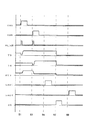
図5は、画像をサンプリングするときの、本発明の実施形態の制御信号を示すタイミングを示す図である。第1の事象51は、信号スイッチトランジスタQ2をパルスするSHS制御線を含む。PRE_DSCH制御線は、放電トランジスタQ1をパルスし、このトランジスタは、信号コンデンサCSを放電させる。信号コンデンサCSが画素セル2の信号電圧VSの電位に充電するとき、信号スイッチトランジスタQ2は、オンのままである。
【0039】
第2の事象53は、基準スイッチトランジスタQ3をパルスするSHR制御線を含む。PRE_DSCH制御線は、放電トランジスタQ1をパルスし、このトランジスタは、基準コンデンサCRを放電させる。基準コンデンサCRが、画素セル2の基準電圧VRの電位に充電されるとき、基準スイッチトランジスタQ3は、オンのままである。
【0040】
第3の事象55は、第1の出力トランジスタQ11をオンにするSHD1制御線を含み、このトランジスタは、緩衝増幅器20の差電圧が、サンプリングされて格納されることを可能にさせる。差電圧は、画素セル2で受け取られている光の強度を表す。緩衝増幅器20は、内部的に固定パターン雑音を減算する。
【0041】
第4の事象57は、等化器トランジスタQ4、Q5をオンにするEQ制御線を含み、これらのトランジスタは、信号コンデンサおよび基準コンデンサを電位VBASEにまで充電することにより、緩衝増幅器20の第1の入力および第2の入力をVBASEに駆動する。緩衝増幅器20の出力は、緩衝器のオフセット電圧に駆動される。
【0042】
第5の事象59は、第2のトランジスタQ13をオンにするSHD2制御線を含み、このトランジスタは、緩衝増幅器20の緩衝器オフセット電圧が、サンプリングされて格納されることを可能にする。
【0043】
図5のDTS線は、前に記述した事象が起こるときの緩衝増幅器20の出力における電位を示す。
【0044】
本発明の具体的な実施形態を記述し、示してきたけれども、本発明は、このように記述し示された部分の固有の形に限られるものではない。本発明は、特許請求の範囲によってのみ、範囲を規定される。
【0045】
本発明は例として次の実施態様を含む。
(1)受け取った光の強度に比例した振幅を持つ信号電圧に出力を駆動するアクティブ画素であって、該アクティブ画素が光を受け取っていない時には、基準電圧に該出力を駆動するアクティブ画素(2)と、
前記アクティブ画素の出力を受け取り、前記信号電圧をサンプリングして格納し、前記基準電圧をサンプリングして格納するサンプルアンドホールド回路(10)と、
前記サンプリングして格納された信号電圧および前記サンプリングして格納された基準電圧の間の差電圧を生成する緩衝増幅器(20)とを備えるアクティブ画素センサの読み出しチャネル。
【0046】
(2)前記緩衝増幅器(20)が、
前記サンプリングされて格納された信号電圧および前記サンプリングされて格納された基準電圧を受け取り、前記サンプリングされて格納された信号電圧および前記サンプリングされて格納された基準電圧の間の差に比例した電位を持つ1つの出力電圧を生成する差動入力シングルエンド増幅段(22)と、
前記1つの出力電圧を受け取り、前記1つの出力電圧の電位に比例する振幅を持つ緩衝器電流を生成する緩衝段(24)と、
前記緩衝器電流を受け取り、前記電圧を生成し、および前記緩衝器電流の振幅より大きい振幅を持つよう予め調整された出力電流を生成する利得段(26)とを備える上記(1)に記載のアクティブ画素センサ読み出しチャネル。
【0047】
(3)前記サンプルアンドホールド回路が、
信号格納要素と、
前記アクティブ画素の出力を前記信号格納要素に接続し、前記信号格納要素が前記信号電圧を格納できるようにした信号電圧スイッチと、
基準格納要素と、
前記アクティブ画素の出力を前記基準格納要素に接続し、前記基準格納要素が前記基準電圧を格納できるようにした基準電圧スイッチとを備える上記(1)に記載のアクティブ画素センサ読み出しチャネル。
【0048】
(4)前記アクティブ画素センサ読み出しチャネルが、前記緩衝増幅器への入力を等化(イコライズ)して、前記緩衝増幅器内のオフセットエラーを判断することができるようにした手段を備える上記(1)に記載のアクティブ画素センサの読み出しチャネル。
(5)前記サンプルアンドホールド回路が、前記基準格納要素により格納された電圧に等しくなるよう、前記信号格納要素により格納された電圧を設定する手段を備える上記(3)に記載のアクティブ画素センサの読み出しチャネル。
【0049】
(6)前記信号格納要素および前記基準格納要素を放電する手段を備える上記(3)に記載のアクティブ画素センサの読み出しチャネル。
(7)前記緩衝段(24)が、ソースホロワーを備える上記(2)に記載のアクティブ画素センサの読み出しチャネル。
(8)前記緩衝増幅器が、1より大きい利得を持つ上記(1)に記載のアクティブ画素センサの読み出しチャネル。
(9)前記信号格納要素が信号コンデンサ(CS)であり、前記基準格納要素が基準コンデンサ(CR)である上記(3)に記載のアクティブ画素センサの読み出しチャネル。
【0050】
(10)前記利得段(26)が、ビット線の配列内の多重ビット線に接続される利得段出力を備える上記(2)に記載のアクティブ画素センサの読み出しチャネル。
【0051】
【発明の効果】
この発明によると、電子的にサンプリングされた画像に関連する固定パターン雑音を除去するアクティブ画素センサを実現することができる。このアクティブ画素センサはの読み出しチャネルは、電子的にサンプリングされた画像を取り込むのにサンプル数を最小にすることができ、チャネル出力の修正時間を改善することができる。
【図面の簡単な説明】
【図1】従来技術のアクティブ画素センサの緩衝増幅器を示す図。
【図2】本発明の実施形態を示す図。
【図3】本発明の実施形態によるサンプルアンドホールド回路の詳細を示す図。
【図4】本発明の実施形態による緩衝増幅器の詳細を示す図。
【図5】本発明の実施形態による制御信号を示すタイミング図。
【符号の説明】
2 アクティブ画素
10 サンプルアンドホールド回路
20 緩衝増幅器
22 差動入力シングルエンド段
24 ソースホロワー段
26 利得段[0001]
BACKGROUND OF THE INVENTION
The present invention relates generally to analog active pixel sensor readout channels, and more specifically to differential input single-ended analog readout channels for current mode gain assisted active pixel sensors.
[0002]
[Prior art]
An electronic camera generally converts an optical image into a set of electronic signals. The electronic signal can represent the intensity of the color of light received by the camera. An electronic camera typically includes an array of image sensors or photodetectors to detect the intensity of light received by the camera. Typically, an image sensor generates an electronic signal that has an amplitude that is proportional to the intensity of light received by the sensor. The electronic signal can be adjusted and sampled for image processing.
[0003]
Integration of image sensors with signal processing circuits has become more important as it allows miniaturization and improvement of imaging systems. The integration of analog and digital signal processing circuits and image sensors allows electronic camera systems to be low cost, compact and low power.
[0004]
Historically, image sensors are primarily charge coupled devices (CCDs). CCDs are relatively small and can provide a high fill factor. However, CCDs are very difficult to integrate with digital and analog circuits. In addition, CCDs consume large amounts of power and suffer from the problem of image smear.
[0005]
Historically, CCDs are photosensitive pixel cells typically used in solid-state visible light imaging device applications. However, a CMOS active pixel sensor with a photogate or photodiode with a signal amplification circuit in a photosensitive pixel cell offers several advantages over CCD. CMOS active pixel sensors consume less power, can be manufactured at lower cost, require lower power supply voltages, and are integrated into large scale integrated circuits than CCDs. Simple. Furthermore, CMOS active pixel sensors can be manufactured at low cost and in a large number of application specific IC (ASIC) processes. Thus, ASIC manufacturers can develop photoelectric pixel cells. As CMOS technology advances, ASIC manufacturers can further reduce manufacturing costs and provide additional performance benefits.
[0006]
FIG. 1 shows a prior art
[0007]
[0008]
The
[0009]
An electronic image is captured by sampling the charge accumulated by each of the photosensitive pixel cells in the array of photosensitive pixel cells. The amount of charge accumulated by each photoelectric pixel cell is proportional to the intensity of light received by the photoelectric portion of the photoelectric pixel cell. The fixed noise pattern of the photosensitive pixel cell reduces the correlation between the sampled value of the charge conducted by the photosensitive pixel cell and the intensity of light received by the photosensitive pixel cell.
[0010]
By sampling the response of the
[0011]
The read
[0012]
Each
[0013]
The
[0014]
[Problems to be solved by the invention]
It would be desirable to have an active pixel sensor that eliminates fixed pattern noise associated with electronically sampled images created by sampling the response of an array of CMOS pixel cells. Ideally, the active pixel sensor readout channel minimizes the number of samples required to capture an electronically sampled image. In addition, an array of photopixel cells manufactured using a standard CMOS process can be used to operate the readout channel of the active pixel sensor. An active pixel sensor readout channel that provides greater current drive than the current readout channel, with a channel output connected to the capacitive bit line.SettlingIt is desirable to improve time. Furthermore, it is desirable to have an active pixel sensor gain factor greater than one.
[0015]
[Means for Solving the Problems]
The present invention provides an active pixel sensor readout channel that is compatible with CMOS fabrication processes. Active pixel sensor connected to single differential output, extended dynamic range, improved current gain, improved current drive and active pixel sensor readout channelbusInterconnectlineProviding a reduced capacitive load. A single differential output reduces the number of samples required for the array of active pixel sensor readout channels to be used to construct an electronic image. Improved current drive allows for the potential generated at the output of the active pixel sensor readout channel.SettlingReduce time.
[0016]
The first embodiment of the present invention comprises a readout channel for an active pixel sensor. The readout channel of the active pixel sensor comprises active pixels. The active pixel drives the output of the active pixel to a signal voltage having an amplitude that is proportional to the intensity of light received by the active pixel. The active pixel drives the output of the active pixel to a reference voltage when the active pixel is not receiving light. Further, the readout channel of the active pixel sensor comprises a sample and hold circuit and receives the output of the active pixel. The sample and hold circuit samples and stores the signal voltage, and samples and stores the reference voltage.The sample and hold circuit includes an equalizer circuit that equalizes the stored signal voltage output and the stored reference voltage output to provide an equalized output voltage.In addition, the readout channel of the active pixel sensor is between the sampled and stored signal voltage and the sampled and stored reference voltage.The first from the differenceGenerate differential voltageAnd a second differential voltage is generated from the equalized output voltage.A buffer amplifier is provided.In addition, a plurality of bus interconnect lines are also provided, wherein the first bus interconnect line receives the first differential voltage and the second bus interconnect line is adapted to correct the offset error of the buffer amplifier. It is selectively connected to the output of the buffer amplifier to receive the second differential voltage.
[0017]
The second embodiment of the present invention is similar to the first embodiment. The buffer amplifier of the second embodiment includes a differential input single-ended amplifier stage that receives a sampled and stored signal voltage and a sampled and stored reference voltage. The differential input single-ended amplifier stage generates an output voltage that includes a potential proportional to the difference between the sampled and stored signal voltage and the sampled and stored reference voltage. The buffer amplifier further includes a buffer stage that receives the one output voltage and generates a buffer current having an amplitude proportional to the potential of the one output voltage. The buffer amplifier further includes a gain stage that receives the buffer current, generates a differential voltage, and generates an output current that is preconditioned to have an amplitude greater than the amplitude of the buffer current.
[0018]
The third embodiment of the present invention is similar to the first embodiment. The sample and hold circuit of the third embodimentCapacitorAnd a signal voltage switch to signal the output of the active pixelCapacitorConnect to the signalCapacitorAllows the signal voltage to be stored. The sample and hold circuit is also a referenceCapacitorAnd reference voltage switch to reference the output of the active pixelCapacitorConnect to the standardCapacitorAllows the reference voltage to be stored.
[0019]
The fourth embodiment of the present invention is similar to the third embodiment. The fourth embodiment is a signalCapacitorAnd standardsCapacitorThe circuit which discharges is provided.
[0020]
Other aspects and advantages of the present invention will become apparent from the following detailed description, taken as an example of the principles of the invention and taken together with the drawings.
[0021]
DETAILED DESCRIPTION OF THE INVENTION
As shown in the figure for clarity, the present invention is embodied in the readout channel of an active pixel sensor. Active pixel sensor readout channel is connected to a single differential output, extended dynamic range, improved current gain, improved current drive and active pixel sensor readout channelbusInterconnectlineWith a reduced capacitive load. A single differential output reduces the number of samples required for the array of active pixel sensor readout channels to be used to construct an electronic image. Improved current drive allows for the potential generated at the output of the active pixel sensor readout channel.SettlingReduce time.
[0022]
FIG. 2 shows a first embodiment of the invention, which comprises the readout channel of the active pixel sensor. The readout channel of the active pixel sensor includes an
[0023]
FIG. 2 shows one
[0024]
FIG. 3 shows another embodiment of the present invention. This embodiment includes a more detailed sample and hold
[0025]
The signal switch transistor Q2 is “on” when the
[0026]
The
[0027]
The output transistors Q11 and Q13 areAOf the readout channel of the active pixel sensorTwo separateOutputs OUT1 and OUT2 are provided. The potential of the first control line SHD1 is positively pulsed to turn on the first output transistor Q11, which connects the differential voltage of the
[0028]
FIG. 3 shows the discharge transistor Q1. The discharge transistor Q1 provides a discharge path for either the signal capacitor CS or the reference capacitor CR when the PRE_DSCH control line pulses to a high potential while the signal switch transistor Q2 or the reference switch transistor Q3 is conducting. In general, the signal capacitor CS and the reference capacitor CR are discharged before the signal voltage or reference voltage is sampled and stored. The potential stored in the signal capacitor CS and the reference capacitor CR is reset by discharging the signal capacitor CS and the reference capacitor CR. This allows the signal voltage and the reference voltage to be stored more accurately. Furthermore, discharging the signal capacitor CS and the reference capacitor CR isSettlingReduce time.
[0029]
The bias transistor Q10 provides a bias voltage for the output of the
[0030]
The
[0031]
The
[0032]
FIG. 4 shows another embodiment of the present invention. This embodiment comprises a more detailed circuit within the
[0033]
The
[0034]
The buffer or
[0035]
Current
[0036]
The size of the source follower transistor MN2 of the
[0037]
Typically, within the array of active pixel sensor readout channels, the outputs of many sensor readout channels are connected to one bit line. The larger the number of sensor readout channels connected to one bit line, the more capacitive load is connected to the bit line. As mentioned before, the capacitance connected to the output of the read channel is the signal voltage at the output of the read channel.SettlingSlow down time. Thus, for each read channel in the read channel arraySettlingThe time can be optimized by minimizing the number of read channels connected to each bit line in the read channel array.
[0038]
FIG. 5 is a diagram illustrating timings indicating control signals according to the embodiment of the present invention when an image is sampled. The
[0039]
The
[0040]
The
[0041]
The
[0042]
The
[0043]
The DTS line in FIG. 5 shows the potential at the output of
[0044]
Although specific embodiments of the present invention have been described and illustrated, the present invention is not limited to the specific forms of the parts so described and shown. The scope of the present invention is defined only by the claims.
[0045]
The present invention includes the following embodiments by way of example.
(1) An active pixel that drives its output to a signal voltage having an amplitude proportional to the intensity of received light, and when the active pixel is not receiving light, an active pixel that drives its output to a reference voltage (2 )When,
A sample and hold circuit (10) that receives the output of the active pixel, samples and stores the signal voltage, and samples and stores the reference voltage;
A readout channel of an active pixel sensor comprising a buffer amplifier (20) that generates a differential voltage between the sampled and stored signal voltage and the sampled and stored reference voltage.
[0046]
(2) The buffer amplifier (20)
Receiving the sampled and stored signal voltage and the sampled and stored reference voltage, and having a potential proportional to the difference between the sampled and stored signal voltage and the sampled and stored reference voltage; A differential input single-ended amplifier stage (22) for generating one output voltage having,
A buffer stage (24) for receiving the one output voltage and generating a buffer current having an amplitude proportional to the potential of the one output voltage;
A gain stage (26) for receiving the buffer current, generating the voltage, and generating an output current that is preconditioned to have an amplitude greater than the amplitude of the buffer current. Active pixel sensor readout channel.
[0047]
(3) The sample and hold circuit is
A signal storage element;
A signal voltage switch that connects the output of the active pixel to the signal storage element so that the signal storage element can store the signal voltage;
A reference storage element;
The active pixel sensor readout channel according to (1), further comprising: a reference voltage switch that connects an output of the active pixel to the reference storage element, and the reference storage element stores the reference voltage.
[0048]
(4) In the above (1), the active pixel sensor readout channel includes means for equalizing an input to the buffer amplifier so that an offset error in the buffer amplifier can be determined. A readout channel of the described active pixel sensor.
(5) The active pixel sensor according to (3), wherein the sample and hold circuit includes means for setting a voltage stored by the signal storage element so as to be equal to a voltage stored by the reference storage element. Read channel.
[0049]
(6) The readout channel of the active pixel sensor according to (3), further comprising means for discharging the signal storage element and the reference storage element.
(7) The active pixel sensor readout channel according to (2), wherein the buffer stage (24) includes a source follower.
(8) The readout channel of the active pixel sensor according to (1), wherein the buffer amplifier has a gain greater than 1.
(9) The readout channel of the active pixel sensor according to (3), wherein the signal storage element is a signal capacitor (CS) and the reference storage element is a reference capacitor (CR).
[0050]
(10) The active pixel sensor readout channel of (2) above, wherein the gain stage (26) comprises a gain stage output connected to multiple bit lines in an array of bit lines.
[0051]
【The invention's effect】
According to the present invention, an active pixel sensor that removes fixed pattern noise associated with an electronically sampled image can be realized. The readout channel of this active pixel sensor can minimize the number of samples to capture an electronically sampled image and improve the channel output correction time.
[Brief description of the drawings]
FIG. 1 shows a buffer amplifier of a conventional active pixel sensor.
FIG. 2 is a diagram showing an embodiment of the present invention.
FIG. 3 is a diagram showing details of a sample and hold circuit according to an embodiment of the present invention.
FIG. 4 is a diagram showing details of a buffer amplifier according to an embodiment of the present invention.
FIG. 5 is a timing diagram showing control signals according to an embodiment of the present invention.
[Explanation of symbols]
2 Active pixels
10 Sample and hold circuit
20 Buffer amplifier
22 Differential input single-ended stage
24 Source follower stage
26 Gain stage
Claims (8)
受け取った光の強度に比例した振幅を持つ信号電圧になるよう出力を駆動するアクティブ画素であって、光を受け取っていない時には、基準電圧に該出力を駆動する、アクティブ画素と、
前記アクティブ画素の出力を受け取り、前記信号電圧をサンプリングして格納すると共に、前記基準電圧をサンプリングして格納する、サンプルアンドホールド回路であって、前記格納された信号電圧の出力と前記格納された基準電圧の出力とを等しくして、等化された出力電圧を提供する等化器回路を含む、サンプルアンドホールド回路と、
前記サンプリングして格納された信号電圧および前記サンプリングして格納された基準電圧の間の差から第1の差電圧を生成する緩衝増幅器であって、該緩衝増幅器の各入力で前記等化された出力電圧から第2の差電圧を生成する、緩衝増幅器と、
複数のバス相互接続線であって、前記緩衝増幅器のオフセットエラーを補正するために、第1のバス相互接続線が前記第1の差電圧を受け取り、かつ、第2のバス相互接続線が前記第2の差電圧を受け取るよう、前記緩衝増幅器の出力に選択的に接続される、複数のバス相互接続線と、
を備える、アクティブ画素センサの読み出しチャネル。An active pixel sensor readout channel,
An active pixel that drives its output to a signal voltage having an amplitude proportional to the intensity of the received light, and that drives the output to a reference voltage when no light is received;
A sample-and-hold circuit that receives the output of the active pixel, samples and stores the signal voltage , and samples and stores the reference voltage, the output of the stored signal voltage and the stored A sample and hold circuit including an equalizer circuit that equalizes the output of the reference voltage and provides an equalized output voltage ;
A buffer amplifier that generates a first differential voltage from the difference between the sampled and stored signal voltage and the sampled and stored reference voltage, the equalized at each input of the buffer amplifier A buffer amplifier for generating a second differential voltage from the output voltage ;
A plurality of bus interconnect lines, wherein a first bus interconnect line receives the first differential voltage and a second bus interconnect line is configured to correct the offset error of the buffer amplifier. A plurality of bus interconnect lines selectively connected to the output of the buffer amplifier to receive a second differential voltage;
A readout channel of the active pixel sensor.
前記サンプリングされて格納された信号電圧および前記サンプリングされて格納された基準電圧を受け取り、該サンプリングされて格納された信号電圧および該サンプリングされて格納された基準電圧の間の差に比例した電位を持つ1つの出力電圧を生成する差動入力シングルエンド増幅段と、
前記1つの出力電圧を受け取り、該1つの出力電圧の電位に比例する振幅を持つ緩衝器電流を生成する緩衝段と、
前記緩衝器電流を受け取り、前記1つの出力電圧を生成すると共に、前記緩衝器電流の振幅より大きい振幅を持つよう予め調整された前記出力電流を生成する利得段と、
を備える、請求項1に記載のアクティブ画素センサの読み出しチャネル。The buffer amplifier is:
Receiving the sampled and stored signal voltage and the sampled and stored reference voltage, and obtaining a potential proportional to the difference between the sampled and stored signal voltage and the sampled and stored reference voltage; A differential input single-ended amplifier stage that generates one output voltage having,
A buffer stage that receives the one output voltage and generates a buffer current having an amplitude proportional to the potential of the one output voltage;
A gain stage that receives the buffer current, generates the one output voltage, and generates the output current preconditioned to have an amplitude greater than the amplitude of the buffer current;
The readout channel of the active pixel sensor according to claim 1, comprising:
請求項2に記載のアクティブ画素センサの読み出しチャネル。The buffer stage comprises a source follower;
The readout channel of the active pixel sensor according to claim 2.
信号コンデンサと、
前記アクティブ画素の出力を前記信号コンデンサに接続して、該信号コンデンサが前記信号電圧を格納することができるようにした、信号電圧スイッチと、
基準コンデンサと、
前記アクティブ画素の出力を前記基準コンデンサに接続して、該基準コンデンサが前記基準電圧を格納することができるようにした、基準電圧スイッチと、
を有する、請求項1に記載のアクティブ画素センサ読み出しチャネル。The sample and hold circuit
A signal capacitor ;
A signal voltage switch, wherein the output of the active pixel is connected to the signal capacitor so that the signal capacitor can store the signal voltage;
A reference capacitor ;
By connecting the output of the active pixel in the reference capacitor, said reference capacitor is to be able to store the reference voltage, the reference voltage switch,
The active pixel sensor readout channel of claim 1, comprising:
Applications Claiming Priority (2)
| Application Number | Priority Date | Filing Date | Title |
|---|---|---|---|
| US09/018,022 US6201572B1 (en) | 1998-02-02 | 1998-02-02 | Analog current mode assisted differential to single-ended read-out channel operable with an active pixel sensor |
| US018022 | 1998-02-02 |
Publications (2)
| Publication Number | Publication Date |
|---|---|
| JPH11275471A JPH11275471A (en) | 1999-10-08 |
| JP4277339B2 true JP4277339B2 (en) | 2009-06-10 |
Family
ID=21785824
Family Applications (1)
| Application Number | Title | Priority Date | Filing Date |
|---|---|---|---|
| JP01641899A Expired - Lifetime JP4277339B2 (en) | 1998-02-02 | 1999-01-26 | Active pixel sensor readout channel |
Country Status (4)
| Country | Link |
|---|---|
| US (1) | US6201572B1 (en) |
| EP (1) | EP0933928B1 (en) |
| JP (1) | JP4277339B2 (en) |
| DE (1) | DE69924312T2 (en) |
Families Citing this family (35)
| Publication number | Priority date | Publication date | Assignee | Title |
|---|---|---|---|---|
| US6529237B1 (en) * | 1997-12-02 | 2003-03-04 | Texas Instruments Incorporated | Complete CDS/PGA sample and hold amplifier |
| US6801258B1 (en) * | 1998-03-16 | 2004-10-05 | California Institute Of Technology | CMOS integration sensor with fully differential column readout circuit for light adaptive imaging |
| US6836291B1 (en) | 1998-04-30 | 2004-12-28 | Minolta Co., Ltd. | Image pickup device with integral amplification |
| US6734907B1 (en) * | 1998-04-30 | 2004-05-11 | Minolta Co., Ltd. | Solid-state image pickup device with integration and amplification |
| US6765613B1 (en) * | 1998-07-22 | 2004-07-20 | Micron Technology, Inc. | Low light sensor signal to noise improvement |
| US6587145B1 (en) * | 1998-08-20 | 2003-07-01 | Syscan Technology (Shenzhen) Co., Ltd. | Image sensors generating digital signals from light integration processes |
| US6563540B2 (en) | 1999-02-26 | 2003-05-13 | Intel Corporation | Light sensor with increased dynamic range |
| JP4358351B2 (en) * | 1999-04-27 | 2009-11-04 | 浜松ホトニクス株式会社 | Photodetector |
| US6753912B1 (en) * | 1999-08-31 | 2004-06-22 | Taiwan Advanced Sensors Corporation | Self compensating correlated double sampling circuit |
| US6453422B1 (en) * | 1999-12-23 | 2002-09-17 | Intel Corporation | Reference voltage distribution for multiload i/o systems |
| US6873364B1 (en) * | 2000-06-08 | 2005-03-29 | Micron Technology, Inc. | Low-power signal chain for image sensors |
| KR100397663B1 (en) * | 2000-06-23 | 2003-09-13 | (주) 픽셀플러스 | Cmos image sensor in which dataline is maintained as data of reset mode |
| US7286174B1 (en) | 2001-06-05 | 2007-10-23 | Dalsa, Inc. | Dual storage node pixel for CMOS sensor |
| US6797933B1 (en) * | 2001-06-29 | 2004-09-28 | Vanguard International Semiconductor Corporation | On-chip design-for-testing structure for CMOS APS (active pixel sensor) image sensor |
| FR2838903B1 (en) * | 2002-04-17 | 2005-08-05 | St Microelectronics Sa | METHOD AND DEVICE FOR READING PHOTOSENSITIVE CELLS |
| US7443427B2 (en) * | 2002-08-23 | 2008-10-28 | Micron Technology, Inc. | Wide dynamic range linear-and-log active pixel |
| US20050174455A1 (en) * | 2004-01-27 | 2005-08-11 | Transchip, Inc. | Column amplifier for image sensors |
| US6873282B1 (en) * | 2004-03-04 | 2005-03-29 | Charles Douglas Murphy | Differential time-to-threshold A/D conversion in digital imaging arrays |
| US20050200730A1 (en) * | 2004-03-11 | 2005-09-15 | Beck Jeffery S. | Active pixel sensor array sampling system and method |
| JP4817354B2 (en) * | 2004-11-05 | 2011-11-16 | ローム株式会社 | Semiconductor chip |
| JP4425809B2 (en) * | 2005-02-03 | 2010-03-03 | 富士通マイクロエレクトロニクス株式会社 | Imaging device |
| US7250893B2 (en) * | 2005-05-17 | 2007-07-31 | Silicon Light Machines Corporation | Signal processing circuit and method for use with an optical navigation system |
| US7765251B2 (en) * | 2005-12-16 | 2010-07-27 | Cypress Semiconductor Corporation | Signal averaging circuit and method for sample averaging |
| US8471191B2 (en) * | 2005-12-16 | 2013-06-25 | Cypress Semiconductor Corporation | Optical navigation system having a filter-window to seal an enclosure thereof |
| US7659776B2 (en) * | 2006-10-17 | 2010-02-09 | Cypress Semiconductor Corporation | Offset voltage correction for high gain amplifier |
| US7742514B1 (en) | 2006-10-31 | 2010-06-22 | Cypress Semiconductor Corporation | Laser navigation sensor |
| JP2008136047A (en) * | 2006-11-29 | 2008-06-12 | Sony Corp | Solid-state imaging device and imaging device |
| US20080204567A1 (en) * | 2007-02-23 | 2008-08-28 | Weize Xu | Sample and hold circuits with buffer offset removed |
| US8063422B2 (en) * | 2008-04-25 | 2011-11-22 | Infrared Newco, Inc. | Image detection apparatus and methods |
| US8541727B1 (en) | 2008-09-30 | 2013-09-24 | Cypress Semiconductor Corporation | Signal monitoring and control system for an optical navigation sensor |
| US7723659B1 (en) | 2008-10-10 | 2010-05-25 | Cypress Semiconductor Corporation | System and method for screening semiconductor lasers |
| FR2943179B1 (en) * | 2009-03-13 | 2016-06-03 | E2V Semiconductors | MOS IMAGE SENSOR AND METHOD FOR READING WITH LOW INVERSION REGIME TRANSISTOR. |
| EP2254330A1 (en) * | 2009-05-18 | 2010-11-24 | Thomson Licensing | Method and system for operating an image data collection device |
| US8836835B2 (en) | 2010-10-04 | 2014-09-16 | International Business Machines Corporation | Pixel sensor cell with hold node for leakage cancellation and methods of manufacture and design structure |
| US11272132B2 (en) | 2019-06-07 | 2022-03-08 | Pacific Biosciences Of California, Inc. | Temporal differential active pixel sensor |
Family Cites Families (8)
| Publication number | Priority date | Publication date | Assignee | Title |
|---|---|---|---|---|
| JP3287056B2 (en) * | 1993-03-24 | 2002-05-27 | ソニー株式会社 | Solid-state imaging device |
| US5471515A (en) * | 1994-01-28 | 1995-11-28 | California Institute Of Technology | Active pixel sensor with intra-pixel charge transfer |
| US5841126A (en) * | 1994-01-28 | 1998-11-24 | California Institute Of Technology | CMOS active pixel sensor type imaging system on a chip |
| US5631704A (en) * | 1994-10-14 | 1997-05-20 | Lucent Technologies, Inc. | Active pixel sensor and imaging system having differential mode |
| EP0757475B1 (en) * | 1995-08-02 | 2004-01-21 | Canon Kabushiki Kaisha | Solid-state image sensing device with common output line |
| US5898168A (en) * | 1997-06-12 | 1999-04-27 | International Business Machines Corporation | Image sensor pixel circuit |
| JP3673620B2 (en) * | 1997-07-18 | 2005-07-20 | キヤノン株式会社 | Photoelectric conversion device |
| US5900623A (en) * | 1997-08-11 | 1999-05-04 | Chrontel, Inc. | Active pixel sensor using CMOS technology with reverse biased photodiodes |
-
1998
- 1998-02-02 US US09/018,022 patent/US6201572B1/en not_active Expired - Lifetime
-
1999
- 1999-01-19 DE DE69924312T patent/DE69924312T2/en not_active Expired - Lifetime
- 1999-01-19 EP EP99300352A patent/EP0933928B1/en not_active Expired - Lifetime
- 1999-01-26 JP JP01641899A patent/JP4277339B2/en not_active Expired - Lifetime
Also Published As
| Publication number | Publication date |
|---|---|
| EP0933928A2 (en) | 1999-08-04 |
| JPH11275471A (en) | 1999-10-08 |
| EP0933928A3 (en) | 2000-11-29 |
| US6201572B1 (en) | 2001-03-13 |
| DE69924312D1 (en) | 2005-04-28 |
| DE69924312T2 (en) | 2006-03-16 |
| EP0933928B1 (en) | 2005-03-23 |
Similar Documents
| Publication | Publication Date | Title |
|---|---|---|
| JP4277339B2 (en) | Active pixel sensor readout channel | |
| US6128039A (en) | Column amplifier for high fixed pattern noise reduction | |
| JP4362156B2 (en) | Sequential correlation double sampling method for CMOS area array sensor | |
| US7183531B2 (en) | Amplification with feedback capacitance for photodetector signals | |
| CN1200555C (en) | Active linear sensor | |
| US7755018B2 (en) | Differential column readout scheme for CMOS APS pixels | |
| US20020149688A9 (en) | MOS-type solid-state imaging apparatus | |
| US7385636B2 (en) | Low noise sample and hold circuit for image sensors | |
| US20080094483A1 (en) | In-pixel kTC noise suppression using circuit techniques | |
| US6667468B2 (en) | MOS-based image sensor and method of forming black-level signal therefor | |
| US5923369A (en) | Active pixel sensor cell with differential amplifier and array including same | |
| JP4243688B2 (en) | Amplification type solid-state imaging device | |
| US20080218620A1 (en) | Ultra low noise cmos imager | |
| CN112312052B (en) | Image sensor with electronic global shutter and differential sensing using reset sampling capacitor shared by multiple image storage capacitors | |
| US20040222351A1 (en) | Multiple crawbar switching in charge domain linear operations | |
| WO2008121232A1 (en) | Sample and hold circuits for cmos imagers | |
| US6781627B1 (en) | Solid state imaging device and electric charge detecting apparatus used for the same | |
| US7268815B1 (en) | Differential readout of a pixel array with elimination of pixel- and column-wise fixed pattern noise | |
| CA2350416A1 (en) | Image sensor with correlated double sampling technique using switched-capacitor technology | |
| US7872676B2 (en) | Methods, systems, and devices for offset compensation in CMOC imagers | |
| US7199828B2 (en) | Active pixel sensor cell array | |
| JP2009278149A (en) | Solid-state imaging device | |
| EP1220534A1 (en) | Image sensor with correlated double sampling technique using switched-capacitor technology | |
| US20030001079A1 (en) | Current mode pixel amplifier | |
| JP2006148455A (en) | Solid imaging apparatus |
Legal Events
| Date | Code | Title | Description |
|---|---|---|---|
| A521 | Request for written amendment filed |
Free format text: JAPANESE INTERMEDIATE CODE: A523 Effective date: 20051025 |
|
| A621 | Written request for application examination |
Free format text: JAPANESE INTERMEDIATE CODE: A621 Effective date: 20051025 |
|
| A711 | Notification of change in applicant |
Free format text: JAPANESE INTERMEDIATE CODE: A711 Effective date: 20070727 |
|
| RD02 | Notification of acceptance of power of attorney |
Free format text: JAPANESE INTERMEDIATE CODE: A7422 Effective date: 20070808 |
|
| A711 | Notification of change in applicant |
Free format text: JAPANESE INTERMEDIATE CODE: A711 Effective date: 20080222 |
|
| A521 | Request for written amendment filed |
Free format text: JAPANESE INTERMEDIATE CODE: A821 Effective date: 20080616 |
|
| RD02 | Notification of acceptance of power of attorney |
Free format text: JAPANESE INTERMEDIATE CODE: A7422 Effective date: 20080616 |
|
| A131 | Notification of reasons for refusal |
Free format text: JAPANESE INTERMEDIATE CODE: A131 Effective date: 20080930 |
|
| A521 | Request for written amendment filed |
Free format text: JAPANESE INTERMEDIATE CODE: A821 Effective date: 20081226 Free format text: JAPANESE INTERMEDIATE CODE: A523 Effective date: 20081226 |
|
| TRDD | Decision of grant or rejection written | ||
| A01 | Written decision to grant a patent or to grant a registration (utility model) |
Free format text: JAPANESE INTERMEDIATE CODE: A01 Effective date: 20090203 |
|
| A01 | Written decision to grant a patent or to grant a registration (utility model) |
Free format text: JAPANESE INTERMEDIATE CODE: A01 |
|
| A61 | First payment of annual fees (during grant procedure) |
Free format text: JAPANESE INTERMEDIATE CODE: A61 Effective date: 20090302 |
|
| FPAY | Renewal fee payment (event date is renewal date of database) |
Free format text: PAYMENT UNTIL: 20120319 Year of fee payment: 3 |
|
| R150 | Certificate of patent or registration of utility model |
Free format text: JAPANESE INTERMEDIATE CODE: R150 |
|
| S111 | Request for change of ownership or part of ownership |
Free format text: JAPANESE INTERMEDIATE CODE: R313113 |
|
| FPAY | Renewal fee payment (event date is renewal date of database) |
Free format text: PAYMENT UNTIL: 20120319 Year of fee payment: 3 |
|
| R350 | Written notification of registration of transfer |
Free format text: JAPANESE INTERMEDIATE CODE: R350 |
|
| FPAY | Renewal fee payment (event date is renewal date of database) |
Free format text: PAYMENT UNTIL: 20120319 Year of fee payment: 3 |
|
| FPAY | Renewal fee payment (event date is renewal date of database) |
Free format text: PAYMENT UNTIL: 20130319 Year of fee payment: 4 |
|
| FPAY | Renewal fee payment (event date is renewal date of database) |
Free format text: PAYMENT UNTIL: 20130319 Year of fee payment: 4 |
|
| FPAY | Renewal fee payment (event date is renewal date of database) |
Free format text: PAYMENT UNTIL: 20140319 Year of fee payment: 5 |
|
| R250 | Receipt of annual fees |
Free format text: JAPANESE INTERMEDIATE CODE: R250 |
|
| R250 | Receipt of annual fees |
Free format text: JAPANESE INTERMEDIATE CODE: R250 |
|
| R250 | Receipt of annual fees |
Free format text: JAPANESE INTERMEDIATE CODE: R250 |
|
| R250 | Receipt of annual fees |
Free format text: JAPANESE INTERMEDIATE CODE: R250 |
|
| R250 | Receipt of annual fees |
Free format text: JAPANESE INTERMEDIATE CODE: R250 |
|
| EXPY | Cancellation because of completion of term |