JP4275223B2 - Power supply - Google Patents
Power supply Download PDFInfo
- Publication number
- JP4275223B2 JP4275223B2 JP29048598A JP29048598A JP4275223B2 JP 4275223 B2 JP4275223 B2 JP 4275223B2 JP 29048598 A JP29048598 A JP 29048598A JP 29048598 A JP29048598 A JP 29048598A JP 4275223 B2 JP4275223 B2 JP 4275223B2
- Authority
- JP
- Japan
- Prior art keywords
- circuit
- switching element
- output
- power supply
- commercial
- Prior art date
- Legal status (The legal status is an assumption and is not a legal conclusion. Google has not performed a legal analysis and makes no representation as to the accuracy of the status listed.)
- Expired - Fee Related
Links
Images


Landscapes
- Dc-Dc Converters (AREA)
- Inverter Devices (AREA)
- Rectifiers (AREA)
Description
【0001】
【発明の属する技術分野】
本発明は、商用交流電源を入力とし、整流し平滑した後に適宜変換して負荷に電力を供給する電源装置の改良に関するものである。
【0002】
【従来の技術】
図4は、従来の直流電源をインバータ回路により数KHz乃至数10KHzの高周波交流電力に変換して出力する電源装置を示す接続図である。同図において、1は、交流電源であり、単相商用交流又は3相商用交流の電源が用いられる。2は交流電源1からの電力を整流して直流に変換する整流回路であり、ダイオード3乃至6から構成されている。C1は整流回路2の出力を平滑するコンデンサ、7はコンデンサC1の出力を高周波交流電力に変換して図示しない負荷に供給するインバータ回路である。13はインバータ回路7を構成するスイッチング素子を交互に導通させる駆動信号を出力するインバータ制御回路である。同図において、交流電源1の出力は、整流回路2にて整流され、コンデンサC1にて平滑されて、インバータ回路7にて高周波交流電力に変換される。
【0003】
図4において、コンデンサC1には整流回路2の出力の最大値が充電されるため、交流電源1の実効出力電圧の約1.4倍の電圧がインバータ回路7に供給される。従って、交流電源1の出力が200乃至230V(以下、200V系統という)の場合、整流し平滑された電圧は280乃至322Vとなるために、インバータ回路7に使用される各素子の定格電圧は600Vのものが使用されている。また、交流電源1の出力が380乃至460V(以下、400V系統という)の場合、整流し平滑された電圧は532乃至644Vとなるために、インバータ回路7に使用される各素子の定格電圧は1000V又は1200Vのものが使用されている。
【0004】
【発明が解決しようとする課題】
上記の従来装置においては、交流電源1が200V系統と400V系統とで、インバータ回路7に使用される素子及び、例えばこのインバータ回路7に接続されるインバータ回路7の出力を変圧するインバータ変圧器等の部品をそれぞれ用意しなくてはならないために、コストが高くなるという不具合を有する。
【0005】
【課題を解決するための手段】
請求項1に記載の発明は、商用交流電源を入力とし、商用交流電源の出力を整流して直流とする整流回路と、整流回路の出力端子間に接続された2個のコンデンサからなる直列回路と、直列回路の正の出力端子に一方の端子が接続された第1のスイッチング素子と、直列回路の負の出力端子に一方の端子が接続された第2のスイッチング素子と、第1のスイッチング素子の他方の端子と直列回路の直列接続点との間に接続された第1のダイオードと、第2のスイッチング素子の他方の端子と直列回路の直列接続点との間に接続された第2のダイオードと、第1のスイッチング素子と第1のダイオードとの接続点と第2のスイッチング素子と第2のダイオードとの接続点との間に接続された平滑回路と、平滑回路の両端子間に接続された入力電力を負荷に適した特性に変換する出力変換回路と、第1のスイッチング素子と第2のスイッチング素子とを所定の導通時間率でかつ商用交流電源が低電圧の系統であるときには同時に、商用交流電源が高電圧の系統であるときには互いに重複することなく交互にON−OFF制御するスイッチング素子制御回路と、商用交流電源が低電圧の系統であるときは2個のコンデンサを並列接続とし商用交流電源が高電圧の系統であるときは2個のコンデンサを直列接続とする切り替えスイッチとを備えた電源装置である。
【0007】
請求項2に記載の発明は、スイッチング素子制御回路が、平滑回路の出力電圧又は出力電流の検出値と設定値との差に応じてON−OFF時間率を決定する回路である請求項1に記載の電源装置である。
【0008】
【発明の実施の形態】
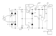
図1は本発明の実施の形態の例を示す接続図である。同図において、1は交流電源であり、単相商用交流又は3相商用交流の電源が用いられる。2は交流電源1からの電力を整流して直流に変換する整流回路であり、ダイオード3乃至6から構成されている。C2及びC3は整流回路2の出力端子間に接続された直列コンデンサであり、コンデンサC2及びC3の容量を等しく設定しておく。8及び9はスイッチング素子、14はスイッチング素子8と9との導通時間率を制御するスイッチング素子制御回路であり、商用交流電源1の電圧が低電圧のときは両者を同時に、また、商用交流電源1の電圧が高電圧のときは両者を重複することなく交互にそれぞれ所定の導通時間率と周波数でON及びOFFを繰り返すための駆動信号を出力する。10及び11はダイオード、C4は平滑用のコンデンサ、7はコンデンサC4の出力を高周波交流電力に変換して図示しない負荷に供給するインバータ回路である。13はインバータ回路7を構成するスイッチング素子を交互に導通させる駆動信号を出力するインバータ制御回路である。
【0009】
図1において、400V系統の商用交流電源を使用する場合について説明する。まず、スイッチング素子8がONしスイッチング素子9がOFFしている間は、交流電源1の出力は整流回路2で整流され、整流回路2の出力は、整流回路2→スイッチング素子8→インバータ回路7→ダイオード11→コンデンサC3→整流回路2の経路を流れる。このとき、インバータ回路7に供給される電圧は、コンデンサC2の充電電圧となり、コンデンサC2びC3の容量が等しく設定されていると、交流電源1の出力を整流し平滑した電圧の1/2の電圧となる。次に、スイッチング素子8及び9がOFFの間は、コンデンサC4に充電された電力が、コンデンサC4→インバータ回路7→コンデンサC4の経路を流れる。次に、スイッチング素子8がOFFしスイッチング素子9がONしている間は、交流電源1の出力は整流回路2で整流され、整流回路2の出力は、整流回路2→コンデンサC2→ダイオード10→インバータ回路7→スイッチング素子9→整流回路2の経路を流れる。このとき、インバータ回路7に供給される電圧は、コンデンサC3の充電電圧となり、交流電源1の出力を整流し平滑した電圧の1/2の電圧となる。この結果、交流電源1の出力を整流し平滑した電圧の1/2の電圧が常にインバータ回路7に供給されることになる。
【0010】
なお、スイッチング素子8及び9のON及びOFFの繰り返し周波数を高く設定すると、コンデンサC4の容量を小さくすることができる。
【0011】
次に、200V系統の商用交流電源を使用する場合は、スイッチング素子8及び9を同時ONさせることにより、インバータ回路7に交流電源1を整流し平滑した全電圧を供給することができる。この結果、200V系統時と400V系統時とにおいて、インバータ回路7には略同じ電圧が供給されることになる。
【0012】
図2は本発明の別の実施の形態の例を示す接続図である。同図において、12はリアクトルであり、15は出力電圧設定器、16は出力電圧検出器、17は比較器である。その他は図1に示した装置と同機能のものに同符号を付してある。同図において、リアクトル12は、コンデンサC2又はC3に流れる電流のピーク値を制限することができ、コンデンサC3及びC4の定格を小さくすることができる。さらに、リアクトル12は、スイッチング素子8及び9に流れる電流のピーク値を制限することができ、スイッチング素子8及び9を過電流から保護することができる。
【0013】
図2において、出力電圧は出力電圧検出器16で検出され、その検出信号Vfは比較器17で出力電圧設定器15の設定信号Vrと比較されて、その差信号△V=Vr−Vfがスイッチング素子制御回路14に供給される。スイッチング素子制御回路14は、入力信号△Vに応じた導通時間率となるように出力パルス幅を決定し、スイッチング素子8及び9を駆動する。この結果、出力電圧は出力電圧設定器15の設定値に対応する値に保たれるようにフィードバック制御されることになり、商用交流電源1の出力電圧の変動や負荷の変動に対して、十分に安定した出力電圧をインバータ回路7に供給することができる。なお、同図において、その他の動作は図1に示した装置の動作と同じであるので、説明を省略する。
【0014】
図2に示したように出力電圧をフィードバックして設定値に一致するように制御するときは、この出力を負荷に適した特性に変換する電力変換回路、図2に示したインバータ回路7、としては、商用交流電源の電圧に無関係に常に特定の電圧が供給されるので、これらの回路として単一の電圧定格のものとすればよいので、回路の標準化ができることになる。
【0015】
図3は本発明のさらに別の実施の形態の例を示す接続図である。同図において、18及び19は切り替えスイッチであり、その他は図1に示した装置と同機能のものに同符号を付してある。同図において、交流電源1として200V系統を使用するときは、切り替えスイッチ18及び19をA側に切り替えて、コンデンサC2及びC3を並列接続にし、交流電源1として400V系統を使用するときは、切り替えスイッチ18及び19をB側に切り替えて、コンデンサC2及びC3を直列接続にする。その結果、交流電源1として200V系統と400V系統とを使用する両方におけるコンデンサC2及びC3による電圧のリップル分を低減する能力を、等しくすることができる。
【0016】
なお、出力電流を設定値に保つ定電流特性とするときには、出力電圧設定器15を出力電流設定器とし、出力電圧検出器16を出力電流検出器とすることによって、両者の差信号を比較器17によって得るように構成し、この差信号によってスイッチング素子制御回路14のパルス幅を決定すればよい。さらに、インバータ回路7の出力電圧や出力電流を目的値に合致させるためには、インバータ制御回路13に出力フィードバック制御機能を持たせてもよいが、図2において、出力電圧検出器16をインバータ回路7の出力電圧を検出するものとすることにより、スイッチング素子8及び9の導通時間率をこの検出値と設定値との差によって決定すれば、スイッチング素子制御回路14によって最終出力の制御が可能となる。この場合、インバータ制御回路13は、単にインバータ回路7の動作周波数を定めるだけで、常に一定の時間率でON−OFF制御するものを用いればよいことになる。
【0017】
【発明の効果】
上記の通り、本発明の電源装置は、交流電源1が200V系統と400V系統とで、インバータ回路7に使用すべき素子及び、例えばこのインバータ回路7に接続されるインバータ回路7の出力を変圧するインバータ変圧器等の部品を共通して使用することができ、200V系統と400V系統とのそれぞれに対応した部品を用いた別機種とする必要がなく、単一の機種でいずれの電源電圧にも適用できるので製作コストの低減をはかることができる。
【図面の簡単な説明】
【図1】本発明の実施の形態の例を示す接続図である。
【図2】本発明の別の実施の形態の例を示す接続図である。
【図3】本発明の更に別の実施の形態の例を示す接続図である。
【図4】従来の電源装置を示す接続図である。
【符号の説明】
1 交流電源
2 整流回路
3、4,5,6 ダイオード
7 インバータ回路
8、9 スイッチング素子
10、11 ダイオード
12 リアクトル
13 インバータ制御回路
14 スイッチング素子制御回路
15 出力電圧設定器
16 出力電圧検出器
17 比較器
18、19 切り替えスイッチ[0001]
BACKGROUND OF THE INVENTION
The present invention relates to an improvement of a power supply apparatus that uses a commercial AC power supply as input, rectifies and smoothes it, converts it appropriately, and supplies power to a load.
[0002]
[Prior art]
FIG. 4 is a connection diagram showing a power supply apparatus that converts a conventional DC power source into high-frequency AC power of several KHz to several tens KHz by an inverter circuit and outputs it. In the figure,
[0003]
4, the capacitor C1 because the maximum value of the output of the
[0004]
[Problems to be solved by the invention]
In the above conventional apparatus, the
[0005]
[Means for Solving the Problems]
The invention according to
[0007]
According to a second aspect of the invention, the switching element control circuit, to claim 1, which is a circuit for determining the ON-OFF time ratio in accordance with the difference between the detected value of the output voltage or output current of the smoothing circuit and the set value It is a power supply device of description.
[0008]
DETAILED DESCRIPTION OF THE INVENTION
FIG. 1 is a connection diagram showing an example of an embodiment of the present invention. In the figure,
[0009]
In FIG. 1, a case where a commercial AC power supply of 400V system is used will be described. First, while the switching element 8 is ON and the switching element 9 is OFF, the output of the
[0010]
Note that if the ON and OFF repetition frequency of the switching elements 8 and 9 is set high, the capacitance of the capacitor C4 can be reduced.
[0011]
Next, when using a 200V commercial AC power supply, the switching elements 8 and 9 are simultaneously turned ON, whereby the inverter circuit 7 can be supplied with the entire voltage obtained by rectifying and smoothing the
[0012]
FIG. 2 is a connection diagram showing an example of another embodiment of the present invention. In the figure, 12 is a reactor, 15 is an output voltage setting device, 16 is an output voltage detector, and 17 is a comparator. The other components having the same functions as those of the apparatus shown in FIG. In the same figure, the
[0013]
In FIG. 2, the output voltage is detected by the
[0014]
When the output voltage is fed back and controlled to match the set value as shown in FIG. 2, a power conversion circuit that converts this output into a characteristic suitable for the load, the inverter circuit 7 shown in FIG. Since a specific voltage is always supplied regardless of the voltage of the commercial AC power supply, these circuits need only have a single voltage rating, so that the circuit can be standardized.
[0015]
FIG. 3 is a connection diagram showing an example of still another embodiment of the present invention. In the figure, reference numerals 18 and 19 denote change-over switches, and the other parts having the same functions as those of the apparatus shown in FIG. In the figure, when the 200V system is used as the
[0016]
When the constant current characteristic is used to maintain the output current at the set value, the
[0017]
【The invention's effect】
As described above, the power supply device of the present invention transforms the elements to be used for the inverter circuit 7 and, for example, the output of the inverter circuit 7 connected to the inverter circuit 7 when the
[Brief description of the drawings]
FIG. 1 is a connection diagram illustrating an example of an embodiment of the present invention.
FIG. 2 is a connection diagram illustrating an example of another embodiment of the present invention.
FIG. 3 is a connection diagram showing still another example of the embodiment of the present invention.
FIG. 4 is a connection diagram showing a conventional power supply device.
[Explanation of symbols]
DESCRIPTION OF
Claims (2)
前記整流回路の出力端子間に接続された2個のコンデンサからなる直列回路と、
前記直列回路の正の出力端子に一方の端子が接続された第1のスイッチング素子と、
前記直列回路の負の出力端子に一方の端子が接続された第2のスイッチング素子と、
前記第1のスイッチング素子の他方の端子と前記直列回路の直列接続点との間に接続された第1のダイオードと、
前記第2のスイッチング素子の他方の端子と前記直列回路の直列接続点との間に接続された第2のダイオードと、
前記第1のスイッチング素子と前記第1のダイオードとの接続点と前記第2のスイッチング素子と前記第2のダイオードとの接続点との間に接続された平滑回路と、
前記平滑回路の両端子間に接続された入力電力を負荷に適した特性に変換する出力変換回路と、
前記第1のスイッチング素子と前記第2のスイッチング素子とを所定の導通時間率でかつ前記商用交流電源が低電圧の系統であるときには同時に、前記商用交流電源が高電圧の系統であるときには互いに重複することなく交互にON−OFF制御するスイッチング素子制御回路と、
前記商用交流電源が低電圧の系統であるときは前記2個のコンデンサを並列接続とし前記商用交流電源が高電圧の系統であるときは前記2個のコンデンサを直列接続とする切り替えスイッチとを備えた電源装置。A rectifier circuit having a commercial AC power supply as an input and rectifying the output of the commercial AC power supply into a direct current;
A series circuit composed of two capacitors connected between the output terminals of the rectifier circuit;
A first switching element having one terminal connected to the positive output terminal of the series circuit;
A second switching element having one terminal connected to the negative output terminal of the series circuit;
A first diode connected between the other terminal of the first switching element and a series connection point of the series circuit;
A second diode connected between the other terminal of the second switching element and a series connection point of the series circuit;
A smoothing circuit connected between a connection point between the first switching element and the first diode and a connection point between the second switching element and the second diode;
An output conversion circuit that converts input power connected between both terminals of the smoothing circuit into a characteristic suitable for a load;
The first switching element and the second switching element are connected to each other at a predetermined conduction time ratio and when the commercial AC power source is a low-voltage system , and simultaneously when the commercial AC power source is a high-voltage system. A switching element control circuit that performs ON-OFF control alternately without performing ,
A switch for connecting the two capacitors in parallel when the commercial AC power source is a low-voltage system and for connecting the two capacitors in series when the commercial AC power source is a high-voltage system; Power supply.
Priority Applications (1)
| Application Number | Priority Date | Filing Date | Title |
|---|---|---|---|
| JP29048598A JP4275223B2 (en) | 1998-10-13 | 1998-10-13 | Power supply |
Applications Claiming Priority (1)
| Application Number | Priority Date | Filing Date | Title |
|---|---|---|---|
| JP29048598A JP4275223B2 (en) | 1998-10-13 | 1998-10-13 | Power supply |
Publications (3)
| Publication Number | Publication Date |
|---|---|
| JP2000125565A JP2000125565A (en) | 2000-04-28 |
| JP2000125565A5 JP2000125565A5 (en) | 2005-11-17 |
| JP4275223B2 true JP4275223B2 (en) | 2009-06-10 |
Family
ID=17756640
Family Applications (1)
| Application Number | Title | Priority Date | Filing Date |
|---|---|---|---|
| JP29048598A Expired - Fee Related JP4275223B2 (en) | 1998-10-13 | 1998-10-13 | Power supply |
Country Status (1)
| Country | Link |
|---|---|
| JP (1) | JP4275223B2 (en) |
Families Citing this family (4)
| Publication number | Priority date | Publication date | Assignee | Title |
|---|---|---|---|---|
| JP4715040B2 (en) * | 2001-06-08 | 2011-07-06 | 富士電機システムズ株式会社 | Semiconductor device |
| JP4766241B2 (en) * | 2005-11-30 | 2011-09-07 | 株式会社安川電機 | DC voltage step-down circuit and power converter |
| JP2007202305A (en) * | 2006-01-26 | 2007-08-09 | Mitsumi Electric Co Ltd | Power supply unit |
| JP5540566B2 (en) * | 2009-05-21 | 2014-07-02 | 株式会社Ihi | Rectifier |
-
1998
- 1998-10-13 JP JP29048598A patent/JP4275223B2/en not_active Expired - Fee Related
Also Published As
| Publication number | Publication date |
|---|---|
| JP2000125565A (en) | 2000-04-28 |
Similar Documents
| Publication | Publication Date | Title |
|---|---|---|
| JP2635820B2 (en) | High power factor double voltage rectifier | |
| JP5394213B2 (en) | Series resonant converter circuit | |
| TWI373900B (en) | High efficiency charging circuit and power supplying system | |
| US5077652A (en) | Dual feedback loop DC-to-AC converter | |
| US20020034083A1 (en) | Zero voltage switching DC-DC converter | |
| JP2001190074A (en) | Power converting device and method | |
| JPH0851790A (en) | Control circuit for inductive load | |
| JPH1198837A (en) | Dc power source apparatus | |
| JPH11127576A (en) | Dc power supply device | |
| KR101742231B1 (en) | High Power Factor And High Efficiency Interleaved Dual-Buck Converter And Method Therefor | |
| JP3161699B2 (en) | DC power supply for arc discharge equipment | |
| JP4275223B2 (en) | Power supply | |
| JPH11235040A (en) | Power supply with three-phase high power factor converter | |
| JPH08275530A (en) | Switching mode power supply | |
| JP2004112954A (en) | Power storage device | |
| US11637492B2 (en) | Buck matrix-type rectifier with boost switch, and operation thereof during one-phase loss | |
| JP5950970B2 (en) | Power converter | |
| JP3369981B2 (en) | Constant sampling type PWM device of sine wave input / output single phase double voltage AC / DC conversion circuit | |
| US5434769A (en) | Multi-phase adaptable AC-DC converter | |
| JP3981208B2 (en) | Arc machining power supply | |
| JP2002084676A (en) | Power conversion device for accumulator | |
| JP2000125548A (en) | Switching power unit | |
| JP3372868B2 (en) | Current control type inverter circuit, control method therefor, capacitor charger and laser device provided with the same | |
| JPH0678535A (en) | Dc power supply equipment | |
| JPS63314176A (en) | Variable voltage/variable frequency power apparatus |
Legal Events
| Date | Code | Title | Description |
|---|---|---|---|
| A521 | Written amendment |
Free format text: JAPANESE INTERMEDIATE CODE: A523 Effective date: 20050927 |
|
| A621 | Written request for application examination |
Free format text: JAPANESE INTERMEDIATE CODE: A621 Effective date: 20050927 |
|
| A977 | Report on retrieval |
Free format text: JAPANESE INTERMEDIATE CODE: A971007 Effective date: 20081121 |
|
| A131 | Notification of reasons for refusal |
Free format text: JAPANESE INTERMEDIATE CODE: A131 Effective date: 20081202 |
|
| A521 | Written amendment |
Free format text: JAPANESE INTERMEDIATE CODE: A523 Effective date: 20081225 |
|
| TRDD | Decision of grant or rejection written | ||
| A01 | Written decision to grant a patent or to grant a registration (utility model) |
Free format text: JAPANESE INTERMEDIATE CODE: A01 Effective date: 20090303 |
|
| A01 | Written decision to grant a patent or to grant a registration (utility model) |
Free format text: JAPANESE INTERMEDIATE CODE: A01 |
|
| A61 | First payment of annual fees (during grant procedure) |
Free format text: JAPANESE INTERMEDIATE CODE: A61 Effective date: 20090304 |
|
| R150 | Certificate of patent or registration of utility model |
Free format text: JAPANESE INTERMEDIATE CODE: R150 |
|
| FPAY | Renewal fee payment (event date is renewal date of database) |
Free format text: PAYMENT UNTIL: 20120313 Year of fee payment: 3 |
|
| FPAY | Renewal fee payment (event date is renewal date of database) |
Free format text: PAYMENT UNTIL: 20120313 Year of fee payment: 3 |
|
| FPAY | Renewal fee payment (event date is renewal date of database) |
Free format text: PAYMENT UNTIL: 20130313 Year of fee payment: 4 |
|
| FPAY | Renewal fee payment (event date is renewal date of database) |
Free format text: PAYMENT UNTIL: 20130313 Year of fee payment: 4 |
|
| FPAY | Renewal fee payment (event date is renewal date of database) |
Free format text: PAYMENT UNTIL: 20140313 Year of fee payment: 5 |
|
| LAPS | Cancellation because of no payment of annual fees |