JP4264984B2 - Radiation detector - Google Patents
Radiation detector Download PDFInfo
- Publication number
- JP4264984B2 JP4264984B2 JP52315999A JP52315999A JP4264984B2 JP 4264984 B2 JP4264984 B2 JP 4264984B2 JP 52315999 A JP52315999 A JP 52315999A JP 52315999 A JP52315999 A JP 52315999A JP 4264984 B2 JP4264984 B2 JP 4264984B2
- Authority
- JP
- Japan
- Prior art keywords
- electric field
- radiation detector
- gas
- electrode
- insulator
- Prior art date
- Legal status (The legal status is an assumption and is not a legal conclusion. Google has not performed a legal analysis and makes no representation as to the accuracy of the status listed.)
- Expired - Lifetime
Links
Images


Classifications
-
- H—ELECTRICITY
- H01—ELECTRIC ELEMENTS
- H01J—ELECTRIC DISCHARGE TUBES OR DISCHARGE LAMPS
- H01J47/00—Tubes for determining the presence, intensity, density or energy of radiation or particles
- H01J47/02—Ionisation chambers
Abstract
Description
本発明は、荷電粒子、陽子、X線および中性子のような電離放射線を正しい位置で検出するために用いることができる非常に高性能な放射線検出器を実施するための改良技術に関する。
気体におけるイオン化と電荷増倍との過程を利用する放射線検出器は、すでに100年前から用いられており、また改良も重ねられてきた。気体検出器において大きな「安定な」比例ゲインを得るための方法は、検出器の業界における恒常的な研究対象である。
数年前、G.チャーパックおよびF.ソーリは、以下の記述においてはMWPCと呼ばれる平行板および多線式比例チェンバーにおけるゲインの限界を克服するための方法として、以後はMSCと呼ばれる多段式チェンバーを導入した。MSCチャンバにおいては、ドリフトしている電子は、従来の気体検出器のドリフト域に取り付けられていて平行板増倍器として作用する2つの平行なグリッド電極によって前置増幅され、そしてこれら電子は主検出要素に送られる。このMSCチェンバーは、感光性の混合気体を用いて動作され、以下の記述ではRICHと呼ばれるリング結像チェレンコフ検出器中において単一の光検出に充分なゲインを達成することができる。
MSCチェンバーおよびRICHチャンバに関するより詳細な点については、我々は以下の刊行物、すなわち、
― G.チャーパックおよびF.ソーリ、Physics Letter 1978年、第78B巻、523ページと、そして
― M.アダムズ等、Nuclear Instrumentation Methods 1983年217巻、237ページ
を参照している。
さらに最近になると、G.チャーパックおよびY.ジオマタリスが、増倍素子として狭間隙平行板アバランシェチェンバーを用いる高ゲイン気体検出器である改良放射線検出器を開発した。、以下の記述では、この放射線検出器をミクロメガスと記す。
このような検出器は一般的には、微細メッシュのある薄い金属の電極を読出し面に平行に引き延ばすことによって得られる50〜100μmの範囲内にある間隙から成る。G.チャーパックおよびY.ジオマタリスは、非常に高い電界中における電極アバランシェの特定の性質から生じると理解されている、非常に高いゲインおよびレート性能を立証した。このミクロメガス検出器に関するより詳細な点については、我々はNuclear Instruments Methods,1996年A376巻29頁に示されているY.ジオマタリス、P.ルブジャール、J.P.ロバートおよびG.チャーパック編の論文を参照している。
上記の両検出器の主要な欠点は、平行なメッシュを非常に高い精度で引き延ばし、そしてそれを維持しなければならない点にある。特に寸法の大きな検出器においては、この問題に加えて強力な静電引力の存在が付け加わる。こうした欠陥を克服するために、重い支持フレームが必要になり、またミクロメガス検出器の場合には間隙に絶縁ラインまたはピンを接近して配置する必要もあり、そのため後の組立が複雑になり、その上、効率のロスも生じる。
最近、もう一つの放射線検出器が、F.バートルその他によって開発され、Journal of Physics III6(1996)、337ページに提案された。
この検出装置は、以下の記述では
![]()
さらに特殊な装置としては、平面天球形(planispherical)のX線イメージ装置のための放射線検出器が現在まで研究されている。この特定の対象に関する最も重要な研究は、ジュネーブ(スイス)にある核研究のための欧州機構においてジョージ・チャーパックによって展開されている。
最初の展開は、球形のドリフトスペースを有する比例チェンバーの特性に関するものであった。
ワイヤチェンバーのドリフトスペース内に適当な球形の等電位面を生成するための抵抗ディバイダを備えている比例ワイヤチェンバーは先ず、スイス、ジュネーブの欧州合同原子核研究所(CERN)のG.チャーパック、Z.ハッダック、A.ジーボン、R.スタッブスによって、そしてフランスのパリ7区のジェネラル・ド・ゴール通り、クレタイユにある多科学センターのR.カーンによって開示され、またNUCLEAR INSTRUMENTS AND METHODS 307巻(1974年)―ジュネーブ、1974年7月29日により刊行された。
また、球形のドリフトスペースを備えた大開口X線イメージチェンバーとして具体化された比例ワイヤチャンバも、ジュネーブのCERNにおいてG.チャーパック、C.ドミエール、R.カーン、J−C.スタンディアールおよびF.ソーリによって開示された。NUCLEAR INSTRUMENTS AND METHODS 141巻(1977年)441〜455頁、North-Holland Publishing Co.を参照されたい。
球形のドリフトスペースは、90°までの受け入れ角を有する球形の入射電極および射出電極として具体化されることが開示されている。球形のドリフトスペースと読出し比例チェンバーとの結合部は、移動スペースTから成ることが開示されており、このスペースTの側壁は、読出し比例チェンバーの第1の陰極電極まで増大する半径を有する球形の等電位面を生成するための抵抗ディバイダを含んでいる。
X線および紫外線のための気体検出器に関する視差誤差の様々な補正法に関する全般的な検討が、スイス、ジュネーブのCERNにおいてG.チャーパックによりなされ刊行されている。NUCLEAR INSTRUMENTS AND METHODS 201巻(1982年)181〜192頁、North Holland Publishing Companyを参照されたい。
更に最近では、ブルックヘーブン国立研究所、ニューヨーク、アップタウン11973のP.リーアック、S.C.スミスおよびB.ユーは、1996年IEEE Nuclear Science Symposium(1996年11月2〜9日、カリフォルニア州アナハイムで開催)において、気体ベースの位置感受性検知器における視差幅の縮小方法を示し、これはIEEE Transactions on Nuclear Science 1997年、第44巻3号、651〜655ページとして刊行されている。
光量子のためのドリフトスペースは入射電極内に限定され、そして読出しチェンバーの陰極ワイヤ面は平坦でかつ平行であるが、読出しチェンバーの入射窓は更に、等電位面を漸進的に湾曲させるために採用された特定の導電パターンを有しており、その結果、焦点から放射するX線の衝突方向がどのようであろうとも、視差誤差を補正しそして減少させるために、電気力線はこの等電位面と90°に交差する。
上記のX線イメージ装置は一般的には、視差誤差が数パーセントに減少している点で満足できるものといえるであろう。しかし、視差誤差の完全な補正を果たすために採用されている導電パターンを備えた読出しチャンバの入射窓は、その実施が困難である。それは、実際の導電パターンとこれら導電パターンに印加される対応電圧は、電界が環形の入射窓の近くでのみほぼ放射状であって、変換領域を構成する等電位の第2の電極に近づくに従って電界はほぼ平行になるからである。その結果、視差誤差は変換X線の貫通と共に増大することになる。
したがって、本発明の目的は、従来技術の放射線検出器における上述の欠点を克服する非常に高性能な放射線検出器を提供することである。
本発明のもう一つの目的は更に、MSCチェンバーの単純さとミクロメガス放射線検出器およびCAT放射線検出器の高電界の利点とを有し、かつ、その実施が機構的により簡単であり、かつ、より多用途の、非常に高性能な放射線検出器を提供することである。
本発明の更にもう一つの目的は、ほぼ1に等しい電荷転送率によって非常に高い精度と解像度が得られる非常に高性能な放射線検出器を提供することである。
本発明のもう一つの目的は、105Hz/mm2までのカウントレートのためのほぼ一定な増幅度を有する放射線検出器を提供することである。
また本発明のもう一つの目的は、特に、イメージ装置が、その入射窓に直交する対称軸に関して完全に対称な構造を有することによって、像の歪みが抑制される視差のない平面天球形のX線イメージ装置に用いられる放射線検出器を提供することである。
更にまた、本発明のもう一つの目的は、特に、従来技術の対応するX線イメージ装置の欠点を克服してしかもその実施が機構的に非常に簡単である特殊な気体電子増倍構造を実現している非常に高性能の視差のない平面天球形のX線イメージ装置に用いられる放射線検出器を提供することである。
本発明によってよって、特に、一次電子が電離放射線によって気体中に解放され、電界によって捕集電極にドリフトする放射線検出器が提供される。本発明の放射線検出器には、複数の電界集束エリア(electric field condensing area)から成る少なくとも1つのマトリックスを含む気体電子増倍装置が含まれていて、これらの電界集束エリアは電界にほぼ垂直な立体面(solid surface)に分布している。各電界集束エリアはそれぞれ、気体中において各一次電子から電子アバランシェを発生させるように局所的に電界振幅(electric field amplitude)を増大させる。このようにして、気体電子増倍装置は、一次電子の所定のゲインをもつ増幅器として作用する。
本発明の目的、利点そしてその他の特徴は、単なる例示として示されている幾つかの実施例について、添付の図面を参照しながら、以下になされる説明を読めば、より明らかになるであろう。
添付の図面において、
― 図1aは、本発明による円筒形の放射線検出器の好ましい1実施例の斜視図である。
― 図1bは、本発明による平面形の放射線検出器の特殊な1実施例の斜視図である。
― 図1cは、本発明による球形の放射線検出器の特殊な1実施例の斜視図である。
― 図2aは、図1aおよび図1bの破線で示されている面Pとして図示されている断面に沿う断面図である。
― 図2bは、図1cにおいて破線で示されている面Pとして図示されている断面に沿う断面図である。
― 図3aは、図2aに対する電気力線を表す図である。
― 図3bは、図2bに対する電気力線を表す図である。
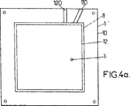
― 図4aは、図1bの細部を示す前面図であり、この細部は、電界集束エリアの1つのマトリックスを含む気体電子増倍装置から成る。
― 図4bは、図4aの細部を示す前面図で、電界集束エリアのマトリックスが複数の円形の通し孔から成ることを非限定的な例示として示されている。
― 図4c、4d、4eおよび4fは、異なる形状とピッチとを有する通し孔を備えたマトリックスの特殊な実施例を示す。
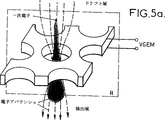
― 図5aは図4bの細部の斜視図で、本発明による放射線検出器内の気体電子増倍装置の動作モードは一次電子から電子アバランシェを発生させるように働くことを示すである。
― 図5bは、図5aにおいて破線で示されている面Rとして図示されている断面に沿う断面図であり、同図において、電気力線および等電位線は1つの局所電界集束エリアの位置で図示され、等電位線は実線で示され、電気力線は破線で示されている。
― 図5cは、図5bに示されている局所電界集束エリア内における電界分布を示すグラフであり、この電界は図5bに示されている対称軸X’Xに関してプロットされている。
― 図6aおよび6bはそれぞれ、本発明による放射線検出器の概略図で、電界集束エリアの複数のマトリックスがこの放射線検出器を実施するために用いられている。
― 図7aは、特定の放射線検出器に挿入される、本発明による気体電子増倍装置の概略図であり、このようにして、本発明のこの気体電子増倍装置は一次電子のための前置増幅器として作用する。
― 図7bは、特定のホスト放射線検出器に組み込まれている、本発明による多段電子増倍装置を表す概略図であり、このようにして、この多段気体電子増倍装置は一次電子のための個別の前置増幅器として作用する。
― 図8aは、本発明による放射線検出器に充填されている幾つかの気体の混合物に対する増幅率を示すグラフであり、この増幅率は局所電界集束エリアのマトリックスに印加されている電圧(ボルト)に対してプロットされている。
― 図8bは、MSSCチェンバーを用いて形成されている本発明による放射線検出器から得られた相対パルス高を表すグラフであり、気体電子増倍装置は図7aに示されているように挿入されていてこの相対パルス高は、Hz/mm2の単位のカウントレートに対してプロットされている。
― 図8cは、アルゴンおよび二酸化炭素の乾燥混合気体とそして湿潤混合気体とがそれぞれ、本発明による放射線検出器内に充填される気体として用いられている場合における本発明による気体電子増倍装置の前置増幅率または増幅率の比較測定値のグラフであり、この増幅率または前置増幅率は分単位の時間に対してプロットされている。
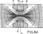
― 図8dには、局所電界集束エリアの中央対称軸に沿った電界の増加が、この局所電界集束エリアの特定ゾーンに注入された永久電荷によって更に増している、局所電界集束エリアの好ましい1実施例が示されている。
― 図9aは、特に結晶学の実験のために用いられる本発明による放射線検出器の前面図である。
― 図9bおよび9cは、より特別に、シンクロトン型の加速器の衝突用リングパス内において加速された衝突粒子によって生成される電離放射線の検出のために設計された本発明による放射線検出器の好ましい1実施例を示す前面図であり、したがって、この加速粒子は非常に高いエネルギーレベルを有する。
― 図10は、より特別に光子検出のための本発明による放射線検出器の非限定的な1実施例の、図3aと同様の断面図である。
― 図11aは、本発明による視差のないX線イメージ装置の好ましい1実施例の断面図である。
― 図11bは、球形の変換領域チェンバー内に生成される一次電子の所定のゲインの増幅器として動作するために特に適している本発明の視差のないX線イメージ装置に組み込まれている気体電子増倍装置の断面であり、これらの一次電子の増幅は電子アバランシェ現象によって生じる。
― 図11cは、本発明の視差のないX線イメージ装置を実施するための入射窓の機械的構造と、気体電子増倍装置の構造とそしてこれらの相対的位置とが示されている図1aの部分斜視図である。
― 図11dは、本発明による視差のないX線イメージ装置を実現する、入射窓および気体電子増倍構造を形成する電極に逐次に印加される電圧を示す電圧分布である。
― 図12aは、本発明の視差のないX線イメージ装置を構成する、球形の変換ボリュームチェンバーと気体電子増倍装置の構造と転送および誘起体積との部分断面図であり、これには、対応する電極と、対応する等電位面とに印加されている相対電圧値が示されている。
― 図12bは、気体電子増倍装置の構造を形成する電界集束エリアの近傍における等電位面および対応する電気力線の局所的歪みがより分かりやすく示されている図2aの細部である。
― 図12cは、より特別に、供給接続線のマスキングによって像の実質的な劣化が生じない逐次導電リングの適正電圧の供給を可能にする本発明の視差のないX線イメージ装置に組み込まれている気体電子増倍装置の構造の断面図である。
本発明による放射線検出器が以下に、当明細書における非限定的な例として開示される。特に、本発明による放射線検出器は、X線撮影や画像診断のような多くの種類の応用に、そしてより一般的には気体に一次電子を解放するために実施されるあらゆる種類の放射線に、同一の利点を持って使用することができる。
以下に、本発明による放射線検出器を図1a、1bおよび1cを参照しながら説明する。
添付の図面においては、同一の参照符号は同一の要素を示すが、全体をより良く理解させるために、これらの図面は、これら要素の相対的寸法を表してはいない。
図1aに示されているように、本発明による放射線検出器は、一次電子が電離放射線によって気体中に解放され、そして、これらの一次電子は、電界によって捕集電極にドリフトされる型の検出器である。上記の図面において、ベクトル
![]()
一般的に、本発明の放射線検出器は、気体が充填されている、参照符号Vで表されている容器を含み、この容器内で入射電離放射線により一次電子が解放される。図1a、1bおよび1cにおいては、電離放射線は、Sという参照符号で表されている発生源によって生成されるX線またはガンマ線として示されている。このようにして、発生源Sにより生成されたX線またはガンマ線は、参照符号IWで表されている入射窓を通って本発明の放射線検出器内に入りそして一次電子を生成し、この一次電子は容器V内に含まれる気体中に解放される。入射窓IWは、一般的には薄い金属フィルムから成るメタルクラッド内部表面を有し、このフィルムはドリフト電位におかれる。以下の記述においては、このドリフト電位をVDと表す。たとえば図1aに示されているように、捕集電極CEと入射窓IWとそしてドリフト電極DEは、気体を収容するための容器Vを形成することができ、一次電子は電離放射線との衝突時にこの気体中において解放される。この容器Vを構成するために参照符号F1およびF2で表されている軽量フレームを用いることもできる。
また、図1a、1bまたは1cに示されているように、容器Vには更に、以下の記載においてGIと記されるガス入口とそしてGOと記されるガス出口とが設けられており、これらは共に、ネジ切りされた1本の小管から成り、後により詳細に説明するように、ガス入口およびガス出口によって特定の混合気体または専用気体を容器Vに充填することができる。ガス入口GIとガス出口GOは、適切な気体充填と循環を保証するために容器Vの両側に配置することもできる。
図1a、1bおよび1cに明示されているように、本発明による放射線検出器は更に、気体電子増倍装置をも備えている。以下、気体電子増倍装置をGEMと記し、参照番号1を付して表す。この気体電子増倍装置1は、複数の電界集束エリアの少なくとも1つのマトリックスを有し、以下、これらの電界集束エリアをそれぞれ1iという参照符号で示す。
上記の図において、電界集束エリアは、電界ベクトル
![]()
![]()
図1bにおいては、図1aと逆に、気体電子増倍装置1は、平面的な形状である立体面によって形成されており、入射窓IWおよびこれに結合しているドリフト電極DEは捕集電極CEと共に、平面的な構造を構成するように、互いに平行である。その結果、捕集電極CEと入射窓およびドリフト電極DEとの間に生成されている電界ベクトル、すなわちベクトル
![]()
図1cにおいては、気体電子増倍装置1を構成している立体面は球形であり、この立体面はこの立体面と平面との交差面によって画定されている。図1aおよび1bと同様に、捕集電極CEと入射窓IWおよびこれに結合しているドリフト電極DEとは球形の形状であって、気体電子増倍装置1を構成している、対応する球形の立体面にほぼ垂直な電界ベクトル
![]()
図1a、1bおよび1cに示されているように、各電界集束エリア1iは、より理解し易いように、1つの孔から成るように表示されているが、ここに生じる局所電界振幅の増大はこの集束エリアの対称軸に関してほぼ対称である。このようにして、この局所電界振幅の増大は各局所集束エリア1iの対称の中心においてほぼ最大になる。本発明の放射線検出器のある特定の実施形態によると、複数の電界集束エリア1iはほぼ同一の形状であり、そうして、図1a〜1cに示されているように、その形状がどのようなものであろうとも、それらの電界集束エリア1iは、気体電子増倍装置1を形成するように、規則的に立体面に分布されている。
次に、図2a、2bおよび3a、3cを参照しながら、本発明の放射線検出器を構成している気体電子増倍装置1の構造および動作モードに関する、より詳細な説明をする。
図2aは、図1aまたは図1bに示されている本発明による放射線検出器の断面図を示しており、この横断面図は、図1aおよび1bにおいて破線で示されている交差面Pに沿って切断したものであり、一方図2bは、図1cにおいて破線で示されている対応する交差面Pに沿った横断面図である。
図2aと2bとを比較すると、気体電子増倍装置1および捕集電極CEと入射窓IWおよびその関連ドリフト電極DEとを構成する立体面が、図2bの放射線検出器においては球形であるので、図2bの同一の要素が湾曲している点においてのみ異なるだけである。いずれの場合でも、捕集電極CEは、本明細書において上述したように、アバランシェの検出ができるように、例えば、プリント回路板上に配置されている金属パッドまたはストリップから成るものと考えられる。
本発明の放射線検出器を形成する気体電子増倍装置の好ましい1実施例においては、図2aおよび2bに示されているように、電界集束エリア1iのマトリックスはメタルが被覆された絶縁物フォイル(参照番号10が付されている)を有する。その絶縁物フォイル10の各面には第1と第2の金属クラッド(それぞれ参照番号11および12が付されている)が形成され、これらの金属クラッド11、12は、絶縁物フォイル10を挟んでいて、正規のサンドイッチ構造を形成している。更に、電界集束エリアのマトリックスには、これらの電界集束エリアを形成するように、規則的サンドイッチ構造(図2aおよび2b参照)を貫通して多くの通し孔(参照番号1i)が設けられている。
更に通し孔の各々の所に1つの電界集束エリア1iを生成するためにバイアス回路が設けられ、該バイアス回路は、第1と第2の金属クラッド11、12に印加されるバイアス電圧を生成する。図2aおよび図2bでは、バイアス回路は参照番号2で表され、そしてVGEMとして示されている電位差を生じさせる。
次に、本発明による放射線検出器の動作モード、特に、図2aおよび図2bに示されている気体電子増倍装置1の動作モードを図3aおよび図3bを参照しながら説明する。
一般的には、規則的サンドイッチ構造は、動作時には、電界ベクトル
![]()
図3aを参照すると、電界ベクトル
![]()
![]()
![]()
![]()
明瞭、かつ、分かり易くするために、図3aおよび3bはドリフト域と検出域内に電荷がないものとして示されているが、このような場合は電離放射線が不在の場合に完全に相当している。例えば、所定の局所電界集束エリアに達する最も外側の電気力線によって画定されている仮想立体面(以下、FTと記す)は、例えば図3aに示されているように、電気力管FTを形成し、その中では、電力束は保存する性質を示す。その結果、各局所電界集束エリア1iの所における電界の増加が次のようにしてなされることは、当該技術に通常の知識をもつ当業者には明らかであろう。すなわち、集束電界のベクトル
![]()
![]()
![]()
図3aにおいて面Qとして参照されている対称面に関して対称な特性を有するサンドイッチ構造によって、任意の局所電界集束エリア1iに達する最も外側の電気力線によって形成される仮想立体面(ドリフト域における仮想立体面)は、同じ電気力管FTに関して、図3aに示されているように、検出域における、同じ局所電界集束エリア1iから出る電気力線によって形成される対称な仮想立体面(対称面Qに関して、ドリフト域における仮想立体面に対称な仮想立体面)としてほぼ写像される。その結果、本明細書において後に説明される、絶縁物フォイル10を挟んでいる第1と第2の金属クラッド11、12に印加される電位差間の所定の関係が達成されると、ドリフト域における曲げられた電気力線の立体面が、図3aに示されているように、検出域内においては完全に復元されることは明らかである。さらに、ドリフト域内における電界
![]()
![]()
![]()
![]()
本発明による放射線検出器を構成する気体電子増倍装置の好ましい実施例を、図4a、4bと、そしてより一般的には図4c〜4fを参照して以下に説明する。例えば図4aに示されているように、気体電子増倍装置1は、参照番号10の薄い絶縁物フォイルによって構成し、該絶縁物フォイルの各面に金属被覆をすることができる。したがって、この金属被覆は図2aおよび2bを参照すると、番号11および12によって表され、このようにして形成されたサンドイッチ構造には、また、番号1iによって表される幾つかの小孔の規則的なマトリックスが貫通している。このフォイルの厚さの典型的な値は25〜500μmで、これらの小孔の中心は50〜300μmの距離で隔てられている。これらの小孔は、20〜100μmの直径を有する。小孔1iのマトリックスは一般的に図4aに示されている規則正しい形状の絶縁物フォイルの中央領域に形成されている。この絶縁物フォイル10はその各面に番号120および110で参照される電極を有し、これらの電極は、小孔のマトリックスを構成しているメッシュの両側の金属面間に電位差を与えるために用いられる。この複合メッシュは、本明細書において後に説明される従来技術によって作製され、設置するに際して簡単であり、頑丈で、そして事故による放電にも強い。
図4aに示されているメッシュは従来のプリント回路技術によって実現することができる。一例として、2枚の同等なフィルムまたはマスクを所望の孔のパターンに形成し、そのフィルムまたはマスクを、予め感光樹脂がコーティングされたメタル被覆絶縁物フォイル10の各側面上に被せる。絶縁物フォイル10はKAPTONまたはこれと同様なポリマーから成る(KAPTONはDUPONT DE NEMOURSの登録商標である)。樹脂被覆を紫外線光に露光し、金属の除去すべき箇所、すなわち小孔になる所のみを酸腐食させる。次にフォイルは、用いられているポリマーにふさわしい溶剤に浸され、化学エッチングによって両側からフォイル内に孔があけられる。エッチングのパラメータの正確な制御は再生可能なメッシュを得るために必須であるが、この全工程は、通常の公知の工業手順を用いる。上述の方法は、例えば20〜100μmの厚さの絶縁物フォイルからメッシュを作製するのに適している。もっと大きな厚さ、すなわち約100〜500μmの厚さの絶縁物フォイルには、プラズマエッチングまたはレーザ穿孔のような代替の標準的製作法を用いることができ、同様な結果が得られる。レーザ穿孔は、本発明に付随する応用にふさわしい形状の小孔マトリックスが得られるように穿孔工程を計算して制御することができるので、特に興味深い方法の1つであるように思われる。
このようにして得られたメッシュの細部は図4bに示されている。図4bに示されている小孔は円形であるが、図4c、4dおよび4eを参照して開示されているように、これらの小孔は様々な形状であり得る。
これらの図面は、メッシュの前面図と、そして当該前面図において小孔のマトリックスを形成している、隣接する2つの小孔の対称中心を含む面に沿って切断した当該前面の断面図とからなる。図4b、4c、4dおよび4eを参照すると、各小孔は20〜100μmの範囲内にある開口部直径をもつものと見なされる。図4bに示されている小孔は円形であり、これらの孔の最も外側の寸法はその開口直径に完全に一致するが、これに反して、図4cおよび4dに示されている小孔は丸い角を有する正方形の孔に完全に一致し、この丸い角が孔の開口直径に相当する。
このような丸い角によって、不規則な放電現象を少なくすることができる。
図4eにおいては、その小孔は、図4bに示されている小孔と完全に対応するように図示されている。図4c、4dおよび4eにおいては、パラメータP、D、d、TおよびSは以下のように定義される。すなわち、
Pは、相次ぐ順序にある2つの小孔の中心間の距離、
Dは、正方形の小孔の最も外側の寸法、
dは、正方形の小孔の最も内側の寸法、
Tは、絶縁物フォイル10の厚さ、
Sは、サンドイッチ構造を形成する第1の金属クラッド11と第2の金属クラッド12の厚さである。
上記のパラメータP、D、d、TおよびSの対応する値は図4cおよび4dに対してマイクロメータの寸法の単位で与えられる。
図4cおよび4dにおける例に示されているように、各通し孔1iは第1と第2の切頭台形の穿孔によって形成されている通し孔から成る。第1の切頭台形の穿孔は、第1の金属クラッド11から、図3a、3bおよび4c、4eにおいて面Qとして示されている規則的サンドイッチ構造の中間面まで延びている。第2の切頭台形の穿孔は、第2の金属クラッド12から、面Qとして示されている同じ中間面まで延びており、切頭台形の穿孔は双方とも、対応する金属クラッド11または12のところで、上述のような所定の値の直径を持つ第1の円形開口を有している。双方の切頭台形穿孔は規則的サンドイッチ構造の中間面のところで連結して、図4cおよび4eに示されている対応する通し孔1iを形成する。上述したような所定の値のピッチPを用いて、同一の形状を有し、かつ絶縁物フォイル10のメタルクラッド面全体にわたって規則的に分布されている通し孔1iは、このようにして、動作中に局所電界集束エリアのマトリックスを構成する小孔マトリックスを形成する。
図4dには、本発明の小孔マトリックスのもう一つの特殊な実施例が示されいる。この場合には、各通し孔1iはその通し孔の縦方向の対称面に沿った円錐体形の断面を有する。
以下に、図4c〜4eに関して、対応するパラメータを記す。
P、TおよびSは、図4cおよび4dの場合と同じパラメータを指す。そして
D1は、例えば、第1の金属クラッド11のところに形成されている小孔の最も外側の寸法、
D2は、第2の金属クラッド12のところに形成されている正方形の小孔の最も外側の寸法、
d1は、第1の金属クラッド11のところにおける絶縁物フォイル10の通し孔の最も外側の寸法、
d2は、絶縁物フォイル10を貫通しかつ第2の金属クラッド12のところにある正方形の通し孔の最も外側の寸法である。
これらの寸法の単位はマイクロメータである。これらのパラメータの値は、寸法例としてのみ表I、IIおよびIIIに記されている。表I、表IIおよび表IIIは、それぞれ、図4cと、図4dと、そして図4eおよび4fとに関連している。

図4fは、各通し孔が完全に円形で貫通されているもう一つの特殊な実施例である。図4fにおける寸法は、したがって、表IIIに示されている寸法に対応することができ、この場合dはDに等しくなる。図4fに示されているようなマトリックスはレーザ穿孔で作製することができる。
次に、本発明による放射線検出器を構成している気体電子増倍装置1のより詳細な動作モードを図5a、5bおよび5cを参照しながら以下に説明する。
動作中において、メッシュの第1と第2の金属クラッド11および12間に電位差が印加されたとき、図3a、3bおよび図5a、5b、5cに示されているように、上述のベクトル
![]()
図3aまたは5a、5bに示されている電界の増加は、図3a、3bまたは5aに示されているドリフト域における電気力管FTの一つに入る一次電子のアバランシェ増倍を誘発するのに充分な大きさである。
図5bは、本発明の目的にしたがって放射線検出器を構成する気体電子増倍装置1の電界集束エリア1iにある電気力線および等電位線の分布を示しており、ここでは電気力線を実線で表し、等電位線を破線で表している。ある所定の電位差VGEMが本発明による放射線検出器を構成する気体電子増倍装置1の第1および第2の金属クラッド11および12に印加されるならば、図5bに明瞭に示されているように、電気力線が第1と第2の金属クラッド11および12にもまた絶縁物フォイル10にも達することがないことは、特に強調しておかなくてはならない。
また、図5bまたは3a、3bにおいてX’Xとして示されている対称軸にそった電界の分布は、図5cに示されているように、図5bの分布曲線に関する対称面である中間面Qに関してほぼ対称であることも、特に強調しておかなくてはならない。セルすなわち電気力管FTの数学的境界を除いてドリフト域からの電気力線はどれも上部電極までで終わるということはないので、局所電界集束エリア1iはドリフト電子を電子アバランシェとして完全に伝達し、このようにして本発明の放射線検出器を構成する気体電子増倍装置1は電荷の完全な伝達を行い、その結果、ほぼ1に等しい電気的透過率を実現することが大切なことである。この電気的透過性は、気体電子増倍装置1を構成するメッシュの光学的透過性とは区別されなければならない。その理由は、ほぼ1に等しいこの電気的透過性は、メタルクラッド絶縁物フォイルの全表面積に対する、局所電界集束エリアを構成する全ての小孔の全表面積の比率として定義される光学的透過率をもつメッシュによって実現され、この光学的透過率は10%〜50%であるからである。また、チャンネルすなわち小孔の高密度によって、電子の拡散に起因する本来の広がりに匹敵する値にまで像の歪みを減少させることができることも強調しなければならない。
次に、図6aを参照しながら、本発明の放射線検出器の特定の一実施例を説明する。
放射線のゲインすなわち増幅率は、本明細書に開示されている気体電子増倍装置によって得られる増幅率のイールドと直接的関係がある。この増幅率は、電界の増加に直接的に関係しており、特に、電界集束エリアを構成する各小孔の対称軸X’Xに沿って電界振幅と、局所電界集束エリア内におけるアバランシェの経路の長さ、したがってメタルクラッド絶縁物フォイル10の厚さに直接的に関係している。本明細書において前述したように、小孔をレーザ処理によって穿孔することによって上記厚さが100μmに達し得る限り、1つの一次電子に対する、検出域に入るアバランシェ電子の数の比率として定義される増幅率の値は、1000以上の値になる。このようなゲインまたは増幅率で、捕集電極CEは例えばイオン化状態においてゲイン1で動作する。このような場合には、この電極CEは、例えば図1a〜1cに示されているように、複数の陽極素子から成り、各々の陽極素子は導電材料の1枚の帯板またはパッドから成り、その導電材料によって各電子アバランシェの電子的検出を行う。例えば図2aおよび図2bに示されている各陽極素子は、基準電位、例えば、グラウンド電位に設定され、上記の図面には示されていない検出装置に検出信号を伝達するための増幅器AにコンデンサCAを介して接続されている。この検出装置は、当該技術に通常の知識を有する当業者にとっては公知であるので、ここでは説明しない。
ほぼ1に等しい上述の電気的透過率のために、本発明の放射線検出器は、一次元の位置検出でも二次元の位置検出でも行うことができる。このような目的のために、図2aに非限定的な1つの例として示されているように、捕集電極CEは、気体電子増倍装置1に面している絶縁物フォイルまたはプリント回路基板上に配置されている幾つかの陽極素子STiを備えており、一次元検出の場合には、各陽極素子はそれぞれ1枚の導電帯板から成り、これらの帯板は互いに平行でありそして第1の方向に延びている。しかし、二次元検出の場合には、絶縁物フォイルの他方の側に更に陽極素子STjを設置することができ、これらは、第1の陽極素子とは別に第1の方向と直交する第2の方向に延びている平行な導電帯板を形成する。気体電子増倍装置1に面している導電帯板STiは、捕集電極CEの全表面積の50%のみを覆うように、互いに規則的に一定の間隔を置いて配置されることが好ましい。それによって、気体電子増倍装置1に面している任意の陽極素子STiの前面に生成される電子アバランシェが、陽極素子STiに部分的にマスクされている、対応する陽極素子STjにも、対応する検出信号を誘起させることができる。コンデンサCAおよび抵抗器RAと共に検出回路を構成する検出増幅器Aのゲインは、それぞれ、陽極素子の各セットに誘起される検出信号の良好な平衡をとるために、各セットの陽極素子に対してそれぞれ異なる適正な値に設定することができる。
本発明の放射線検出器を構成する気体電子増倍装置のゲインイールドを改善するために、図6aに示されているように、電界集束エリアの複数の相継ぐマトリックス(以下、順次配列マトリックスと記す)を用いることができる。これらのマトリックスは一次電子の流れに対してカスケード関係になっており、図6aにおいては、理解を助けるためにGEM1およびGEM2として参照される2つのマトリックスのみが示されている。これらの順次配列マトリックスは互いに平行に、すなわち、交差せずに配置されており、図6aに示されているように、共通の中心に対して相似(homothetic)のマトリックスを形成して放射線検出器を形成している。この図に示されているように、相次ぐ2つのマトリックスは、対応する電界に平行な方向に、所定の距離だけ互いに隔てられて配置されている。その結果、ドリフト電極DE、第1のマトリックスすなわち第1の気体電子増倍装置GEM1、第2のマトリックスすなわち第2の気体電子増倍装置GEM2、さらにそれに続くマトリックスは捕集電極CEと共に、それらの間に、ベクトル
![]()
![]()
![]()
図6aおよび6bに示されている順次配列マトリックスによって形成されている気体電子増倍装置は、このようにして増幅器として動作し、そのゲインは各マトリックスのゲインイールドの積である。図6bは事実上、図6aに示されている放射線検出器の平面的な実施例を示す。図6bに示されているような平面的な実施例では、共通の中心Cは実際上無限遠にあることを想起すべきである。
図1a〜6bを参照して今までに説明された本発明の放射線検出器は増幅器として完全に作用し、その捕集電極CEはゲイン1で動作し、したがって、簡単でかつ非常に安価な裸のプリント回路で作ることができ、そのため、1段気体電子増倍装置でも図6aと6bとに示されている多段気体電子増倍装置でも、全ゲインすなわち増幅率は気体電子増倍装置のみから得られる。
本発明の放射線検出器を実施するためのもう一つのモードを、図7aおよび7bを参照しながら以下に説明する。この場合には、気体電子増倍装置は、適当なゲインをもつホスト検出器に挿入されている。このホスト検出器は一般的に、非限定的な実例として、以後はMSGCと呼ばれる公知のマイクロストリップ気体チェンバー、またはマルチワイヤ比例チェンバーから成る。図7aに示されているように、MSGCの場合には、捕集電極CEは、順次に配列されている陽電極(記号ANとして表されている)と、陰電極(記号COとして表されている)からなり、これらは捕集電極CEを形成するように、誘電支持体に交互に配置され分布されている。各陽電極ANは抵抗器RAを介してグラウンド電位として引用される基準電位に接続され、そして検出できるように増幅器Aにも接続される。一方、陰電極COの各々はバイアス電位発生器VCに接続される。このようにしてMSGCチェンバーは、各陰電極と陽電極間の増幅によって得られるゲインに依存するMSGCチェンバー自身のゲインを有する。更に図7aに示されているように、第1のドリフト域drift1と第2のドリフト域drift2とを形成するために、ドリフト電極DEと捕集電極CEとの間に更に1つの気体電子増倍装置1が挿入されており、これら2つのドリフト域はこの気体電子増倍装置1によって互いに分離されている。
比例計数器、マルチワイヤチェンバー、そしてマイクロストリップ気体チェンバーは全て、電子アバランシェ増倍の基本的増幅過程を利用するが、それらの構造と性能においてのみは異なっているけれど、安全に到達できる最大増幅率は、多くのパラメータに依存しており、そして大きすぎるゲインすなわち大きすぎる電圧が用いられている場合、突発的で危険な放電の確率によって制限される。
一例として、薄くて脆弱な金属帯板で作られているマイクロストリップ気体チェンバーは、特に放電により損傷されやすいように思われる。図7aに示されている増幅器Aのような、帯板に接続されている精巧な電子回路もまた、これらの放電によって不可逆的な損傷を受ける恐れがある。
例えばマイクロストリップ気体チェンバー内に図7aに示されているような気体電子増倍装置1を、適度の電界の影響の下で気体中でドリフトしている電子の経路に挿入することによって、第1のドリフト域drift1に生成されている一次電子を引っ張って、局所電界集束エリアを形成する小孔に送り、そして高い局所電界内でこれらの電子をアバランシェに増倍させ、他方の側から、すなわち、第2のドリフト域drift2内に、これらの電子を押し出し、こうして一次電子を数100倍の倍率で増倍させる効果を生じる。
したがって、本発明の気体電子増倍装置1は、放射線検出器の捕集電極CEの上流(一次電子を供給する側)にある一次電子に対して所定のゲインの前置増幅器として作用する。
ドリフト電極DEおよび捕集電極CEに対して、特に図7aに示されている陰電極COおよび第1と第2の金属クラッド11および12におけるバイアス電位が独立であれば、このような構造は、前置増幅をする気体電子増倍装置1への電離電子の制御された注入を可能にするばかりでなく、気体電子増倍装置1とマイクロストリップ気体チェンバーまたはマルチワイヤ比例チェンバーとの独立した動作を可能にする。
このような動作モードは前置増幅法と呼ばれ、検出される電子を大きく増加させるために用いられる。マルチワイヤまたはマイクロストリップ気体チェンバーと組み合わせれば、はるかに容易に、かつ、安全に少量の電荷を検出することができる。気体電子増倍装置1と、対応する形状のマルチワイヤ比例チェンバーまたはマイクロストリップ気体チェンバーとの組合せは、これらチェンバーの形状を球形または円筒形の気体電子増倍装置に対応させることによって実施することが可能であるが、本発明の気体電子増倍装置1の前置増幅動作法は、平面的構造のマルチワイヤ比例チェンバーまたはマイクロストリップ気体チェンバーの場合に、最も有利であるように考えられる。このような場合においても気体電子増倍装置1は、図7aに示されている平坦な構造に対応する。
気体電子増倍装置が増幅モードで動作している図6aまたは6bについては、図7bに示されているように、幾つかの順次配列の気体電子増倍装置を組み合わせることは、これらの気体電子増倍装置が独立に動作するようになっている限り、非常に興味深いことのように思われる。それは、各要素を中程度の増幅率に独立に設定し、したがって内部的にはより安全に動作するように設定し、これらの要素を順次配列することによってゲインを増大させることが可能になるからである。図7bに示されているように、符号GEM1およびGEM2で表されている順次配列されている2つの気体電子増倍装置が開示されている。各気体電子増倍装置GEM1、GEM2はゲインすなわち増幅率を100に設定されている合成気体電子増倍装置を形成している。したがって、合成増幅率は各ゲインの積であり、10,000に等しい値をもつことになる。
その動作モードとは無関係に、図6a、6bまたは図7a、7bに示されている本発明の放射線検出器を動作させるために、電圧を以下の値に設定することができる。すなわち
― 図6aまたは6bの捕集電極CEの導電帯板はグラウンド電位として引用される基準電位に、
― 図7aまたは7bの捕集電極CEの陽電極ANはグラウンド電位である基準電位に、
他の電位は全て基準電位すなわちグラウンド電位に関連して設定される。下記の電位値は、図8aに示されているように、所定のA−CO2(アルゴン・2酸化炭素)混合気体、厚さ50μmの絶縁物フォイル10と直径100μmの小孔を実現するための所定の気体電子増倍装置の幾何学的構造に対する非限定的な一例として与えられている。この気体電子増倍装置は、大気圧の混合気体の中で動作させられる。パラメータの変化があれば、下記の電位値の範囲の相関的変化を生じる。
― 図7aまたは7bにおける各陰電極COに印加する陰極電位VC=−500V、
― V4は−100V〜−1000Vに設定、
― V3は、電位差VGEM=−500Vのとき、−600V〜−1500Vに設定、
― V2は、−1600V〜−2300Vに設定、
― V1は、VGEM=−500Vのとき、−2100V〜−2800Vに設定。
気体電子増倍装置をドリフト電極から離す距離、または気体電子増倍装置をその次に配列される電極CEから離す距離は3mmに設定された。
本発明による多段式検出器は、増幅モードまたは前置増幅モードで動作しているときには、このように、気体環境で動作していることを除けば、マルチダイノード光電子倍増管と機能的に同様の役割を果たす。しかし、局所電界集束エリアの各マトリックス要素は、マルチダイノード光電子倍増管よりは遙かに大きなゲインを有する。
引き延ばした幾つかの平行な金属メッシュで作られている同様の気体装置、いわゆる平行板多段チェンバーと比較すると、本発明の対象である気体電子増倍装置は、検出器またはホスト検出器内のこの気体電子増倍装置の正確な位置に係わりなく、絶縁物フォイルの厚が一定であることによって増倍ギャップ、したがってゲインがほぼ一定に保たれるので、完全に自立(self-supporting)している。そのうえ、重い支持フレームの必要がない。このことによって、コストを削減しながら、構造を非常に単純化し、信頼性を増加させることができる。
増幅モードで、またはホスト検出器と組み合わせて動作している幾つかのタイプおよびモデルの気体電子増倍装置、すなわち自立している気体電子増倍装置としてのメッシュに関して、広範にわたる実験的な測定がなされている。これらに関しては、以下に列挙されている論文に記載されている。
・Nuclear Instrum.Methods,Methods in Phys.Res.A386(1997)531;F.SAULI
・IEEE Trans.Nucl.Sci.NS-(1997);R.BOUCLIER,M.CAPEANS,W.DOMINIK,M.HOCH,J-C.LABBE,G.MILLION,L.ROPELEWSKI,F.SAULI and A.SHARMA;
・CERN-PPE/97-32;R.BOUCLIER,W.DOMINIK,M.HOCH,J-C.LABBE,G.MILLION,L.ROPELEWSKI,F.SAULI,A.SHARMA and G.MANZIN
・Progress with the Gas Electron.Multiplier,CERN-PPE/97-73;C.BUETTNER,M.CAPEANS,W.DOMINIK,M.HOCH,J-C.LABBE,G.MANZIN,G.MILLION,L.ROPELEWSKI,F.SAULI,A.SHARMA
これらの実験的測定中において、2酸化炭素、メタンおよびジメチルエーテルのような有機または無機の急冷材を加えた、ヘリウム、アルゴン、キセノンなどのような多くの稀ガスおよびこれら稀ガスの混合気体について、100以上の前置増幅率が観測された。図8aは、気体電子増倍装置の増幅率の幾つかの例を示している。これらの増幅率は本発明による1つの気体電子増倍装置を構成する第1と第2の金属クラッド11および12に印加される電位差VGEMに対してプロットされている。図8aに示されている実験結果は、以下のような第1の混合気体について記されている。すなわち、
― アルゴンとジメチルエーテル、アルゴン90%とDME10%、以下、A−DMEと記す、
― アルゴンと2酸化炭素、アルゴン90%とCO2の割合、10%、以下、A−CO2と記す、
― ヘリウムとメタン、ヘリウム70%、メタン30%の割合、以下、He−CH4と記す、
― アルゴンとジメチルエーテル、アルゴン50%とDME50%の割合、以下、A−DMEと記す。
上記の割合は体積比である。
第1と第2の金属クラッド11および12に印加される電位差は200〜約600Vである。以下、この電位差をVGEMと記す。
ほとんど全ての測定は、軽量で安全な検出器の製造と動作に適している大気圧で行われたが、数ミリバールから10バールまでの間で、その正しい性能は満足すべきものであることが判明した。
本発明の放射線検出器を構成する気体電子増倍装置の基本的な性質は、実際に生じるゲインに影響を及ぼさずに局所電界集束エリアのマトリックスを形成するメッシュに印加することのできる電界の強さは、広範囲であるということであるように思われる。このような特性は、非常に重要であると考えられる。その理由は、この特性によって、本発明の放射線検出器が周囲の電極における大きな機械的変化にほとんど影響されないからである。その結果、このような特性によって、電子のドリフト速度、拡散時間と捕集時間の値のような物理的要件を最適にするようにドリフト域を選択することが可能になる。
高レート使用の際に気になることは、検出される電流が大きいという条件のもとで、本発明による放射線検出器を構成する気体電子増倍装置の挙動である。ほとんどの電荷、電子および陽イオンは、装置の動作に影響を及ぼすことなく、開かれている気体のチャンネル(通し孔)中で円滑にドリフトするが、幾つかの漂遊電荷が絶縁体の表面に集まることがある。そのため、このような漂遊電荷は電界をゆがませ、得られるゲインにも影響を与える。しかし、1%を越えない少量の水蒸気をガスに添加することによってチャンネル内の非常に小さな表面導電性を簡単に得ることができ、その表面導電性によって107Hz/cm-2以上の検出X線束まで動作を安定化させることができることが判明している。
イオン注入または半導体層の真空蒸着のような、表面導電性を所望の値に増大させる他の方法が研究されている。その結果、1012〜1013Ω×cmの固有抵抗をもつ、絶縁物フォイル10を構成するポリマーフォイルを用いることによって、自然に、上記の電荷蓄積問題を解決することができることが観測された。
図8dに示されているように、各小孔すなわち通し孔1iは、絶縁物フォイル10によって区画されている内側面を有している。図8dに明瞭に示されているように、この内側面には、1012〜1013Ω×cmの固有抵抗を有する1つの局所領域が含まれることが好ましい。非限定的な一例として、図8dに示されているように、この局所領域は、陽イオンのような電荷が例えばイオン注入によって導入されている切頭台形の通し孔の端末部を覆っていると考えられる。
図8dを参照すれば、当該技術に通常の知識を有する当業者には明らかなことであろうが、絶縁物フォイルの切頭台形の端末部に注入されている陽電荷の存在により、(これらの電荷は小孔の周囲全てに、すなわち図5bを参照しながら既に述べた中間面、すなわち、対称面Qの近傍に、ほぼ同じ濃度で分布されている)電気力線は図8dに示されている中間面すなわち対称面Qのところで非常に密になっており、したがって、注入された電荷の存在によって修正された立体面すなわち電気力管FT内におけるその電力束の保存特性によって、電界は増加される。
軟X線または高速粒子によって気体中に解放される電荷の量を検出するには、現代の高集積度エレクトロニクスの限界により、約100個の電子、10000程度の増幅率が必要である。これは、ゲイン100で安全に動作するマルチワイヤまたはマイクロストリップ気体チェンバーに、増幅率100の気体電子増倍メッシュを組み合わせることによって実現可能である。ホスト検出器における電極(ワイヤまたは帯板である)の離散的な性質によって、電子アバランシェの局所化を達成することが可能になる。
上記のことは、増幅器として動作する下記のような放射線検出器によるか、または、例えば図6aまたは6bに示されている多段式気体電子増倍装置によって達成されることも、当該技術に通常の知識を有する当業者には明らかなことであろう。この場合には、上記放射線検出器において、捕集電極CEがゲイン1に設定され、気体電子増倍装置1は、10,000に等しい増幅率の対応する値を生じるように充分な厚さを持っており、したがってサンドイッチ構造の厚さはほぼ500μmに等しい厚さに達している。
本発明の放射線検出器を構成する気体電子増倍装置のもう一つの基本的性質は、その高レート性能であり、一方、この放射線検出器のゲインまたは相対的パルス高はその全定格範囲においてほぼ一定の値を維持している。
本発明の放射線検出器を構成する気体電子増倍装置のゲインは、一次電子の電子数すなわち気体電子増倍装置を構成するマトリックスの各局所電界集束エリアにおける入口面に入る電子の数に対する、出口面から離れる電子アバランシェにおける電子数の比として定義される。しかし、このようなゲインの数値を求める演算の1つのモードは、一例を挙げれば、外部の55Fe線源によって放射された5.9keV線に対する転送スペクトル(transfer spectra)と直接スペクトル(direct spectra)との間の最も確率の高いパルス高の比として定義される前置増幅率、または増幅率を測定することである。
図8bに示されているように、マイクロストリップ気体チェンバーから成るホスト検出器内に挿入された気体電子増倍装置の3種の動作モードにおいて、相対的パルス高PHは以下の状況において、Hz/mm2を単位として表したレートに対してプロットされている。すなわち
― マイクロストリップ気体チェンバー(MSGC)のみ、
― 気体電子増倍装置(GEM)のみ、そして
― マイクロストリップ気体チェンバーと気体電子増倍装置との組合わせ(MSGC+GEM)。
図8bに示されている結果によれば、電荷ゲイン対する高レート性能は、達成可能な最高レート、約105Hz/mm2まで数パーセントの誤差範囲内で基本的に一定であることが明瞭に確認される。したがって、図8bの結果は、動作モードに係わりなく、局所電界集束エリアにおける短時間のイオン誘導電荷蓄積効果や電荷空間効果がないことを示している。
気体電子増倍装置の局所電界集束エリア中に、またこのエリアを通って後退するイオンの割合は、印加される電圧に依存することに注意を払うべきである。マイクロストリップ気体チェンバーのゲインを1に設定し、気体電子増倍装置のみを動作状態におく動作モードでは、下方の気体内に陽イオンは生成されず、そして恐らく基板の電荷蓄積やエージングの問題は生じないであろう。
気体電子増倍装置より成る本発明の放射線検出器のもう一つの基本的特徴は、時間依存性のゲイン変動がないことでる。
増倍チャンネルすなわち小孔に近い絶縁体材料の存在は、電荷の蓄積による動的ゲイン変動とそのため電界の変動の可能性を生じさせる。しかし、本明細書において上述されているように、所定の比率の水蒸気が導入されている湿潤混合気体を用いるか、または各小孔の内部の所定領域に特定の値の導電性を与えて適切な局所電界集束エリアを形成することによって、この欠点を完全に克服することができる。
図8dに示されているように、例えば陽イオンを注入する上記の後者の解決法に関しては、図8dに示されている対称軸X’Xに向かう電子アバランシェによって生成される可能性のある陽電荷を反発する効果が生じ、それによって、絶縁物フォイルの内側面の電荷蓄積現象を減少させることがきる。しかし、電子アバランシェの電子は、注入されたイオンの存在によって全く影響されない。絶縁物フォイルの内側面によって蓄積される残留電荷は、このようにして電界の全ひずみに対する寄与を劇的に減少させ、したがって電荷蓄積現象は克服される。
図8cは、本発明の目的である気体電子増倍装置1のパルス増幅率の変化を示す図である。同図で、増幅率は、気体電子増倍装置1が実際に動作している時間に対してプロットされており、時間は分単位である。
対応する曲線Iは、サンドイッチ構造の、第1と第2の金属クラッド11および12に、420Vに設定された電位差を印加して動作する気体電子増倍装置に関する曲線であって、放射線検出器は、72%対28%の比のアルゴンと2酸化炭素の混合気体が充填されている。
電荷蓄積現象は、初期値が40に等しいパルス増幅率を、放射線検出器の始動20分後には52以上、またはほぼこれに等しい値に増大させる結果を生じる。
対応する曲線IIは、この混合気体に更に0.35%の水蒸気が加えられていることを除いて、曲線Iを得るために用いられたものと同じ放射線検出器に関する曲線である。
曲線IIは、本発明の放射線検出器が動作している間中ずっと、すなわち実験開始時から50分後の終了時まで、パルス増幅率がほぼ40に等しいという完全一定特性を明らかに示している。
水蒸気を加えた後に、気体電子増倍メッシュの電極間の固有抵抗は10分の1に、、100GΩから10GΩまで次第に減少し、それから一定になることを理解すべきである。チャンネルの全エリア、そして特にチャンネルを構成する小孔の全エリアを考慮すると、曲線IIは明らかに、最も高いレートとして、電荷蓄積現象を除去するのに充分な値は約1016Ω/平方の表面固有抵抗であることを示している。水蒸気を加えた後における固有抵抗の初期値は、最終値と同様に、小孔の全エリア面積とその数に依存している。上記の数値は、約5×105の小孔を備えている10×10cm2の気体電子増倍装置1に関するものである。
特殊な応用に適している幾つかの特定の実施例を、図9a、9bおよび9cを参照しながら以下に説明する。
上述の実施例は、本明細書において上述された増幅モードでも前置増幅モードでも、充分に動作することができる。非常に高エネルギーレベルの電離放射線が研究対象である応用には、増幅モードが好ましいことを更に強調しなければならない。
図9aには、気体電子増倍装置1を形成するサンドイッチ構造が球形である本発明の放射線検出器が示されている。この放射線検出器は、図1cに示されている放射線検出器に相当し、その外形は図9aの前面図で示されているように円形である。この放射線検出器は、X線が結晶に向けて放射される結晶学の試験用のもので、したがって本発明の放射線検出器は結晶へX線が入射することによって発生する回折パターンを完全に検出することができるようになっている。図9aに明瞭に示されているように、電界集束エリアを形成する通し孔は、放射線検出器に関してはBZと呼ばれる少なくとも1つのブラインド検出帯を形成するように、絶縁物フォイルのメタルクラッド面の一部のみに規則的に配分されている。したがって、ブラインド検出帯はほぼ球形であってサンドイッチ構造の中心部分に配置され、通し孔は、このブラインド検出帯の外の回折パターンのみの検出を行うことができるように、このブラインド検出帯の周囲全体に分布されている。特に、図9aに示されている本発明の放射線検出器が増幅モードで用いられている場合、すなわち最終増幅器としてのマイクロストリップ気体チェンバーやマルチワイヤ比例チェンバーがないとき、捕集電極CEの形状を必要に合わせることが可能である。例えばこの電極を帯板、パッドまたはリングで構成する。特にリングは結晶回折の測定の場合に適している。図9aでは、その図面をより理解しやすくするために、捕集電極CEを形成するリングは破線で示されている。
図9bおよび9cはより特殊な場合として、スイス、ジュネーブの欧州合同原子力研究機関(CERN)で稼働中であるものと同様な衝突ビーム加速器または超高速粒子衝突リング加速器に適合している本発明による放射線検出器に関する。図9bおよび図9cにおいて、衝突リング加速器は、曲率半径が大きいので、直線部分として表現されている。図9bおよび図9cに示されているように、本発明による放射線検出器を構成する気体電子増倍装置は、隣接する複数の基本立体面から作られている1つの立体面から成り、各基本立体面は、記号RD1〜RD9によって参照される基本検出器を形成するように、電界集束エリアの少なくとも1つのマトリックスを含む1つの基本気体電子増倍装置を形成する。この基本検出器は、図9bおよび9cに示されている衝突リング加速器を囲む3次元放射線検出器を形成するように、互いに結合されている。
図9bに示されている3次元放射線検出器は球形であり、そして複数の基本放射線検出器から形成されており、これら基本放射線検出器はそれぞれ形状は球形であり、そして図1cに示されている本発明の放射線検出器に完全に一致している。基本検出器RD1、RD2、RD3およびRD4は、スカルキャップを形成するように設計されており、その他の基本検出器は対応する球形体の一部として設計されている。基本検出器RD2およびRD3は、すでに図9aで示されているように、中央ブラインド検出帯を有することも可能である。このブラインド検出帯は更に、衝突リング加速器が貫通できるように穿孔されている。各基本放射線検知器は、本発明によるどのような放射線検出器または基本放射線検出器を製造するために必要な全ての構成要素、例えば、入射窓およびドリフト電極、サンドイッチ構造、捕集電極CEおよび中間フレームを熱成形することによって、図1cに示されている放射線検出器として制作することができる。図9bまたは9cに示されている1つの基本放射線検出器を構成するために、図1aまたは1cに示されているようなガス入口GIとガス出口GOは取り除かれ、そして通し孔と換えることができる。その場合には、通し孔は、図9bにおけるRD2およびRD5のような2つの隣接する基本放射線検出器のガス入口とガス出口を形成する。これらの通し孔は互いに対向して設けられ、そしてOリングによって密封される。図1aおよび1cに示されている第1と第2の金属クラッド11および12によって形成されている入口面および出口面に電位差を印加するための電極端子は少なくされ、そして更に2つの隣接する連続基本放射線検出器のそれぞれ第1と第2の金属クラッド11および12を相互接続させる。このようにして同じ電圧が、各基本放射線検出器を構成する各気体電子増倍装置に印加され、その結果同じゲインが得られる。
更に図9aに示されているように、1つずつの総合ガス入口GIとガス出口GOのみが設置され、その位置は衝突リング加速器の近辺のブラインド検出帯に密接していることが好ましい。電極110および120についても同様で、これらの電極の1つずつのみが配置され、同じ電位差VGEMが第1と第2の金属クラッド11と12とに印加される。
図9cは、ほぼ円筒形をなしている3次元放射線検出器に関する。同図の放射線検出器の両端にはそれぞれ2つの半球形の放射線検出器が接している。この半球形の基本放射線検出器は、以後、記号RD1、RD2、RD8、RD9で示される1つまたは複数の基本放射線検出器によって構成することができる。基本放射線検出器RD1およびRD9は、図9bにおけるRD2およびRD3のような基本検出器と同じ役割を果たしている。図9cに示されている円筒形部分の長さは、衝突リング加速器に沿って数メータにわたって延びている。この円筒形の部分は、幾つかの隣接する基本放射線検出器から成る。以後、これらの基本放射線検出器を、記号RD3乃至RD7で表す。大寸法の3次元放射線検出器が動作できるようにするために、図9bおよび9cに示されているこれら検出器の内部は、各基本放射線検出器の入射窓の外側に、非常に高いエネルギーのX線またはガンマ線に対してほぼ透明なフォーム(foam)を充填することができる。
気体電子増倍装置を素粒子実験の分野に使用することができる、本発明による非常に高い効率の放射線検出器が上述のように開示された。
一般的に、例えばマイクロストリップ気体チェンバー内に設置されている気体電子増倍装置を有し前置増幅モードで動作している、本発明による放射線検出器を実施することによって、従来技術より遙かに安全な条件で、このような精巧ではあるが脆弱な装置を動作させることが可能になる。
本発明の目的にしたがった気体電子増倍装置を実施するための幾つかの新な実験が実際に行われた。
第1の新しい公認の実験(以下、HERA-B AT DESY in Hamburg,Germany(DESY,for Deutsche Elektron Synchrotron)と記す)は、高レートホスト追跡検出器の信頼性を改善するために、本発明の気体電子増倍装置を適当と認めそして採用した。
第2の新しい公認の実験(以下、COMPASS at CERNと記す)は、同様の理由で本発明による気体電子増倍装置テクノロジーを採用することになった。
提案されたもう一つの新たな実験(以下、FELIXと記す)は、ジュネーブのCERN(欧州合同原子核研究機関)で行われ、増幅モードで動作している円筒形構造の放射線検出器を改善するために実施されている。
もう一つの検出器(以下、HELLAZと記す)は、単一電子を検出するのに充分に大きなゲインを達成する目的で、GRAN SASSO社のイタリア研究所の大規模な宇宙線実験のために提案されている。
本発明の放射線検出器のさらにもう一つの特殊な使用には、外部電圧の制御により電子およびイオンの双方または一方の移送を妨げることも含まれる。図2aおよび2bに示されているように、バイアス発生源2は、共通スイッチKによって切り換えることができる逆の極性を有する2つの電圧発生器からなる。スイッチKを操作すると、電子およびイオンの双方または一方が移送を妨げるられるように、電位差VGEMを逆転させることができ、したがってサンドイッチ構造は活性ゲートとして作用する。このようにして増加された電界は、所定の荷電イオンまたは電子を反発する程充分に強力になる。
本発明の目的にしたがった放射線検出器のさらにもう一つの実施例を図10を参照しながら以下に説明する。
この実施例は、より特殊な実施例で、外部発生源によって放射された光子の放射線検出器としてのものである。
本発明の目的にしたがった、光子検出器として作用する気体電子増倍装置1の動作原則は、以下のようなその構造の特性に基づいている。すなわち
― 増幅器または前置増幅器として作用し、そして本明細書において上述の気体電子増倍装置を含む複合構造における様々な電極に印加される電位に実際上は依存する、0から1までの制御された電気的透過性と、
― 製造時における適切なパターニングによって得られる約10から50%までの幾何学的構造によって制御される光透過性と、
― 光電陰極材料に実際上無害であることが分かっている純粋で不活性な気体中におけるゲインに関して実証されている動作と、そして可視または不可視の多くの特殊な波長において動作し、気体環境で高い量子効率と長い寿命とを有する光電陰極材料材の存在。
図10には、本発明の目的にしたがったリバース光電陰極、気体電子増倍装置、そして光子検出器の概要が、それに対応する特徴および電気力線と共に示されている。
例えば図3aを参照して本明細書に上述されているように、本発明の目的である光子のための放射線検出器は1つの容器を備えている。この容器は、分かり易くするために図10では省略されているが、電界によって一次電子から電子アバランシェを発生させるための気体が充填されている。
さらに、記号Cとして表されている透明電極に連結されている入射窓IWが設置されていて、この入射窓および透明電極は、容器内に含まれている気体中に光子を透過するように準備されている。入射窓IWと透明電極Cは、光子の波長に対してほぼ透明である材料から作られている。入射窓IWと透明電極Cとを結合するために公知の技術を用いればよい。この理由で透明な電極Cは図10において破線のみで示されている。
さらに上記の図に示されているように、透明電極Cに面して光電陰極層(参照記号PhC)がある。この光電陰極層は、光子の1つがそれぞれこの光電陰極層に衝突すると一次電子として1つの光電子を発生させるように形成されている。
気体電子増倍装置1は、本明細書において前記したように、少なくとも1つの電界集束エリアのマトリックスを含むように準備されている。該マトリックスは、両面に金属クラッド11、12を備えているメタルクラッド絶縁物フォイル10から形成され、金属クラッド11は透明電極Cに面している。図10に明瞭に示されているように、光電陰極層PhC、金属クラッド11、12およびメタルクラッド絶縁物フォイル10は、本明細書に上述したような正規のサンドイッチ構造を形成する。そのうえ、複数の通し孔(参照符号1i)が当該正規のサンドイッチ構造を貫通し、これらの通し孔の各々を通って、気体と、そしてこの気体の中で生成された荷電粒子とが自由に流れることができる。実際に図10に示されている気体電子増倍装置1を実施するためには、先ずメタルクラッド絶縁物フォイル10の両面を金属クラッド11および12で被覆し、これらの金属クラッドの面の一方に、光電陰極層PhCを構成するために感光材料の層を堆積させる。次に、本明細書において現に開示されている技術のいずれかにしたがって、通し孔を穿孔することができる。
図10に示されているように、入射窓IWと透明な電極Cは、図3aのドリフト域と同様に作用する移送域を形成するために、間隔を置いて配置されている。このことは、本明細書において後により詳細に説明される。
本発明の放射線検出器は更に、容器の底部側に、検出域内に生成される電子アバランシェの位置の検出を行うように設計されている検知ユニットを有する。検出域は、図10に示されているように、気体電子増倍装置1と検知ユニットとの間に形成されている。検知ユニットは、分かりやすいように、図2aまたは図3aを参照して上述した捕集電極CEとして図示されている。分かりやすいように図10には示されていないけれど、検知ユニットは、例えば上述の多段式気体電子増倍装置、またはマイクロストリップ気体チェンバーまたはマルチワイヤ比例チェンバーでさえもを形成するために、もう1つの気体電子増倍装置を備えることができることを強調したい。
一方、図10に示されているように、捕集電極CEの上部電極には幾つかの陽極素子が配置され、これらの陽極素子は、それぞれSTiと記されている。これらの陽極素子は、例えば、平行な導電帯板からなり、それらの導電帯板は、FCEと表示されている絶縁物フォイル上に配置されている。さらに、前掲の抵抗器RA、コンデンサCAおよび増幅器Aから成る電子回路も設けられている。
更に図10に示されているように、参照符号B1のバイアス回路が設置されている。この回路は、発射された光子の各々が光電陰極層PhCと衝突して生成される光電子を引き出すために、透明電極Cおよび第1の金属クラッド11を、基準電位に対してほぼ同じ電位に維持するように作用する。したがって、バイアス回路B1は、図では、短絡回路として表されている。
参照符号B2で示されているもう一つのバイアス回路も設けられている。このバイアス回路B2は、各通し孔のところで前掲の電界集束エリア1iを形成するように金属クラッド11と12との間に印加される電位差VGEMを発生する。このような電圧を印加することによって、各電界集束エリアにおいてベクトル
![]()
もう一つのバイアス回路(参照符号B3)も設けられている。後に説明されるように電子アバランシェを検出できるように、金属クラッド12と捕集電極CEとの間に、また、さらに特定すれば、図10においてSTiと表わされている陽極素子との間に実際に印加されるバイアス電圧を生成する。以下に説明するように、このバイアス電圧によって電子アバランシェの検出が可能になる。
先ず、捕集電極CEの一部を形成する各陽極素子STiは、抵抗器RAによってほぼ基準電位に設定されていることを想起してほしい。この抵抗器RAは、対応する各陽極素子を基準電位に接続する非常に高い抵抗値をもつ抵抗器である。
図10に示されている放射線検出器の動作モードを、この図を参照しながら以下に説明する。
透明電極Cと、この透明電極に面している金属クラッド11とを、バイアス回路B1によって同じ電位値に維持することによって、図3aに示されている電界ベクトル
![]()
その結果、各電界集束エリア内に生成されたそれぞれの集束電界ベクトル
![]()
![]()
![]()
![]()
透明電極Cを光電陰極層PhCから隔てている距離と、金属クラッド12を陽極素子STiから隔てている距離とは、それぞれ移送域と検出域を限定している。これらの距離は、図3aを参照しなら説明した値と全く同じであり、したがって、対応する電位も同じ値に設定されている。その結果、電位差VGEMを500Vに設定し、金属クラッド12と陽極素子STi間に印加される電圧は1,000Vに設定される。これらの値は一例として挙げられたものである。
更に図10に示されているように、電界集束エリア1iを通過する電子アバランシェの位置検出は2次元検出として実施されることが好ましい。捕集電極CEの内側面は第1のセットの陽極素子STiが設けられているが、同じ捕集電極CEの外側面はこれもまた平行な導電帯板から成るもう一つのセットの陽極素子STjが配置されていて、2つのセットの陽極素子STiとSTjは、それぞれ互いに直交する方向における二次元検出を可能にするように、対応する直交する方向に延びている。
光子用の多段式放射線検出器を実施するために、さらにもう1つの気体電子増倍装置を用いる場合には、孔の中の高電界の所でアバランシェ過程で増倍された電子は更に増幅されるために第2の増幅要素にドリフトする。
1段方式であっても多段方式であっても、他の公知の気体検出器では得ることができないこの放射線検出器の基本的特性は、気体電子増倍装置の各電界集束エリアを形成する通し孔内の一次増倍においても、第2段階要素内の2次増倍においても、電子アバランシェ過程の間に生成された2次光子は、光電陰極層PhCを熱することはなく、それによって、2次放射が誘起されることを防止することができるということである。
このようにして、通し孔内で生成される双極子の高電界によって、1に近い電気的透明度と0に近い光学的透明度の収集効率を得ることができる。
孔エリアに対する全エリアの大きな比率は、また、金属クラッド11の表面のほとんどが光感知材によってコーティングされ、その結果、1に近い幾何学的量子効率を有することを意味している。金属クラッド12と陽極素子STi間の大きな電位差によって得られる電界分布によって、最終増幅段階で生成される陽イオンの小部分のみしか実際に光電陰極層PhCに達することができず、したがって損傷効果を減少させることができる。
本発明が目的とする光子用の放射線検出器は、このようにして、
― 広いエリア全体の大きな量子効率と、そして
― 光子のフィードバックはなく、そのうえイオンのフィードバックは非常に小さい大きなゲイン
とを同時に得ることを可能にする。
多段式気体電子増倍装置の場合における2つの増幅要素の全総合ゲインは、このようにして、単一光電子の検出と位置測定とを行うために充分な値に設定することができる。このことは、チェレンコフリング結像、イメージ増幅器、可視または近紫外領域における蛍光分析、または広いエリアにおける光子の検出および位置測定を必要とする応用のような数多くの科学的、技術的または工業的応用に道を開くものである。
本発明の目的にしたがった気体電子増倍検出装置は、前置増幅モードでも増幅モードでも、堅固で、かつ、簡単な構造を有するので、工業的診断または医学的診断に放射線の低レートおよび高レートの検出および位置測定が用いられる多くの分野における応用が期待される。
最後に、本発明の放射線検出器を構成する気体電子増倍装置を製作するために用いられる現在のテクノロジーは化学エッチング、プラズマエッチング、またはレーザ穿孔によってメタルクラッドに孔を開けることに依っているが、将来の技術発展によって、例えばミクロ細孔フィルタのような微細な孔を有する絶縁メッシュに導体をコーティングすることになるかも知れない。
医学的診断では、以下のような幅広い、対応する医学分野がある。すなわち
― 放射線およびβ線のクロマトグラフィと、電子を放出するアイソトープで標識付けをされた分子が解剖標本または吸い取り紙上の拡散標本に含まれている電気泳動と、除去標識を付けられている分子における組織に関してまたは電界の効果により台紙に拡散している物質の分子量に関して情報を提供するスライドサンプルについて測定された二次元放射線の分布。
― 広いエリア全体にわたる軟X線のエネルギーと放射点に関する情報を同時に得られる性能が考古学および美術鑑定における材料分析のために利用できる位置依存蛍光分析。
― 気体電子増倍検出器が結晶化された分子の回折パターンの位置と強さを視差の歪みなしに写像することができる球形の配置において実現される蛋白質結晶学。専用のシンクロトロン放射線施設で高レートが達成可能である。
― 2次電子放射コンバータに連結された時の本発明による気体電子増倍装置が、柔らかい組織のX線撮影のために用いられるX線の吸収プロフィールをサブミリメートルの解像度で効果的に写像できる乳房造影。
― 高放射線束粒子ビームが、露光前または露光中に空間およびエネルギー損失プロフィールを完全に確認できる療法に用いられる高放射線束ビーム診断。そのような応用においては、ビーム特性の動的制御が可能である。
本発明の放射線検出器のもう一つの可能性は、加速器またはこれと同等なものにおいて真空ビーム管との関連をもつことに関する応用または特定の需要そして特に特殊な切欠きを有するその形状に合わせて気体電子増倍装置を特製する可能性にも関している。
上述の広い医学的応用分野のうちでも、本発明の気体電子増倍装置において最も重要なのは、視差のないX線イメージ装置を実施することであるように思われる。
より特殊な実施態様として、本発明によって、X線イメージ装置の入射窓に照射するために円錐形のX線を生成するように、平行なX線ビームが結晶に向かって放射される視差のない平面天球形のX線イメージ装置が提供される。X線イメージ装置は、入射窓を通して電離される電離気体を収容する容器を有する。
このX線イメージ装置には更に、容器内に、入射窓と結合している球形の変換体積チェンバー(spherical conversion volume chamber)が含まれている。この変換体積チェンバーには、動作中に球形の当該変換体積チェンバー内に球形の等電位面および対応する半径方向の電気力線を生成するための第1と第2の平行な電極が含まれており、これらの球形の等電位面はそれぞれ、球形の変換体積チャンバ内に一次電子を発生し、該一次電子が半径方向の電気力線に沿ってドリフトすることができるように、ほぼ結晶の位置に一致するフォーカス共通中心点を中心にしている。第3の電極は、第2の電極にほぼ平行に設けられ、第2,第3の電極は、協働して気体電子増倍装置を形成する。この気体電子増倍装置は、1つの立体面に配分されている幾つかの電界集束エリアからなる少なくとも1つのマトリックスを有する。気体電子増倍装置構造が一次電子に対して所与のゲインの増幅器として動作することができるように、各電界集束エリアは、気体中で一次電子の1つから電子アバランシェを生成するために適正な局所電界振幅の増加を生成するように設計されている。更に、読出電極が設けられ、該読出電極は電極素子の配列を備え、その電極素子の配列は、容器の壁上に形成されていて第3の電極に平行に配置されている。
X線イメージ装置は、また、その容器の外側に、電気的バイアス回路を有し、該電気的バイアス回路は、第1、第2、第3の電極と接続され、球形の変換体積チャンバ内で一次電子をドリフトさせ、次に、気体電子増倍構造内においてアバランシェ現象により、ドリフトされている対応する一次電子を増倍させるように、適当な電圧を出力するように構成されている。また検出回路も設置されていて、実質的な視差の読出し現象がない気体電子増倍構造によって、発生したアバランシェ現象の位置の2次元読出しができるように、読出し電極に接続されている。
以下に非限定的な一例として、本発明による特定の放射線検出器を構成する視差のないX線イメージ装置を開示する。特に、本発明による視差のない平面天球形のX線イメージ装置は、様々な種類の応用、例えば蛋白質構造の分析およびゲノム特性の決定のために用いられる、結晶から拡散されたX線の回折パターンの結像、乳房撮像のための医学診断に用いれる低線量吸収X線撮影、工業的な吸収性のある後方散乱X線撮影、そして周囲の物質から放射される光子によるぼけのある物体内の特定域の結像などに用いることができ、特定の利点があることに留意すべきである。
より特定の実施形態として、入射窓を照射する円錐形のX線ビームとして放出され、気体中において一次電子を解放する効果があるどのような種類の放射線も、本発明の視差のない平面天球形のX線イメージ装置によって検出することができる。
次に図11a、11bおよび11cを参照しながら、本発明による視差のない平面天球形のX線イメージ装置を開示する。
添付の図面においては、対応する要素の相対的寸法は、全体の理解のために表されてはいない。
図11aは、本発明の視差のない平面天球形のX線イメージ装置の断面図である。この断面図は、図11aの平面に一致する対称面内に表示されている。本発明の視差のないX線イメージ装置は、円筒形状で実施されることがより好ましく、したがってこの対称面は、当明細書において後により詳細に説明されるように、この円筒の半径方向対称面に相当する。
図11aに示されているように、本発明の視差のない平面天球形のX線イメージ装置は、このX線イメージ装置の入射窓(参照記号IW)を照射する円錐形のX線ビームを生成するように、結晶に向けらる平行なX線を用いて使用される。
更に図11aに示されているように、本発明のX線イメージ装置は、容器Vを有し、該容器Vには、入口すなわち入射窓IWを通過して容器V内にX線ビーム特に円錐形X線ビーム(円錐形X線ビームについては、当明細書において更に説明されている)が入射したときに、一次電子を生成するための電離気体が充填されている。当明細書において上に述べたように、容器Vは円筒形であり、したがってその入射窓IWは円形で、平坦であり、そして入射する円錐形のX線ビームの方を向いている。
図11aに示されている本発明のX線イメージ装置は、また更に、入射窓IWに結合している、球形変換体積チェンバー(参照符号SPC)を有する。変換体積チェンバーSPCは、平行な第1の電極と第2の電極とを備え、この第1の電極と第2の電極とは、動作中に、球形の等電位面およびそれに対応する、半径方向を向く電気力線FLをこの球形変換体積チェンバーSPC内に生成するように構成されている。
その結果、本発明の視差のないX線イメージ装置の最も重要な特徴の1つによれば、変換体積チェンバーSPCは、その等電位面が球形の形状であるので、完全に球形の変換体積チェンバーとして作用するが、それは完全に平面的な構造または正方形の構造を有するのみである。したがって、このような長方形または平面的な構造は、実施が極めて簡単であるけれど、当明細書において後に説明されるように、このような長方形の、または平面的な構造を構成している電極に印加される電位を適切にとることによって、球形の等電位面の形の微調整が行われる。
本発明による視差のないX線イメージ装置に本質的な特徴の1つによれば、等電位面ほそれぞれ参照符号FPで表されているフォーカス共通中心点(focus common centered point)をその中心にしており、この中心点は、球形変換体積チェンバーSPC内に生成された一次電子が半径方向の電気力線に沿ってドリフトすることができるように、動作中においてはほぼ結晶の位置に一致する。
図11aにおいては、半径方向の電気力線は1本だけ示されているが、この電気力線は、変換体積チェンバーSPC内の点線で示されている球形の等電位面に完全に直交している。この電気力線は図11aではFLという記号が付けられている。
第1と第2の電極に加えて、本発明による視差のないX線イメージ装置を構成する容器には更に、第2の電極にほぼ平行である第3の電極が含まれており、これらの第2と第3の電極は、参照記号GEMの気体電子増倍構造を形成し、一次電子のための所定ゲインの増幅器として動作する。
一般的に、この気体電子増倍構造GEMには複数の電界集束エリア(参照符号Ciで表されている)からなる1つのマトリックスが含まれ、これらの電界集束エリアCiは立体面の内部に分布されており、この立体面は容器V内に含まれている上述の第2と第3の電極によって区画されている。
この構造GEMは図11bに示されており、そしてその動作モードは図3aの動作モードとほぼ一致する。しかし、図11bにおいてはドリフト電極DEは第1の電極1と記され、第1と第2の金属被覆はそれぞれ第2と第3の電極2および3と記され、そして捕集電極CEは読出し電極4と記されている。
図11bにより詳細に示されているように、上記立体面は、プリント回路基板によって実施することも可能であり、そして各面に金属被覆されている薄い絶縁物フォイルからなることも好ましい。この金属被覆は、参照番号2および3を付され、容器内に含まれている第2と第3の電極を構成する。このようにして形成されたサンドイッチ構造は、また、図11bにおいては参照記号Ciで表されている複数の小孔からなる正規のマトリックスによって貫通されている。この絶縁物フォイルの典型的な厚さは25〜500μmで、小孔の中心は距離50〜300μmだけ隔たっている。小孔は、20〜100μmの直径を有する。小孔のマトリックスは一般的に、標準形状の絶縁物フォイルの全エリアまたは大部分のエリア内に形成されている。したがって、絶縁物フォイルはその各面に電極を配置され、これらの電極は第2の電極2と第3の電極3を形成し、そして小孔マトリックスを構成するメッシュの金属側面間に電位差を印加する。
複合メッシュは当明細書において上述した従来技術によって作ることができ、そして堅牢に設置することが簡単にでき、事故による放電にも抵抗があると考えられる。
小孔マトリックスを構成するメッシュは、従来のプリント回路技術で実現することができる。
小孔マトリックスの構造、これら小孔の寸法と形状、気体または混合気体の種類、そしてGEM構造の対応する動作モードは当明細書においてすでに開示されている。
第2の電極2と第3の電極3は、適宜な電位差、すなわち、この立体面内に小孔マトリックスを形成する各小孔のところで各小孔に対応する電界集束エリアCiを形成するために連続的な電位差に設定されるように形成されている。
サンドイッチ構造を貫通する各小孔または通し孔は、実際上は付加的な電界ベクトル
![]()
![]()
その結果、各電界集束エリアは、円錐形のX線ビームの射線の1つが入射したときに球形変換体積チャンバ(参照記号SPC)内において生成される一次電子から気体中に1つの電子アバランシェを生成するために適切な局所的電界振幅の増加
![]()
図を明瞭にし、かつ、より良く理解をするために、図11bは、ドリフト域内すなわち球形変換体積チェンバーSPC内と、そして検出域に相当する移送および誘起体積チェンバー(参照記号TIVCで表されている)内に電荷が存在しない状態で表示されている。この場合は、例えば電離放射能が存在しない場合に相当する。図11bを参照すると、例えば図11aに示されている1つの局所電界集束エリアに到達する最も外側の電気力線によって区画されている、以後はFTと呼ばれる仮想立体面は電気力管FTを形成し、電気力管FT内では、電力束が保存される性質を示す。その結果、各局所電界集束エリアのところで電界が増加することは、当該技術に通常の知識のある当業者には明らかであろう。この場合には、集束電界のベクトル
![]()
![]()
![]()
電界集束エリアCiのマトリックスを構成するサンドイッチ構造は、図1bにおいて平面Qとして表されている対称面に関して対称な性質を有していることを強調しなければならない。その結果、ある局所電界集束エリアCiに到達する最も外側の電気力線によって形成される仮想立体面は、同じ電気力管FTに関して、図1aに示されているように、検出域における同じ局所電界集束エリアCiを離れる電気力線によって形成された対称な仮想立体面としてほぼ写像される。
更に図11aに示されているように、本発明による視差のないX線イメージ装置は、容器V内に、また好ましくはこの容器Vの壁部に形成された信号読出し電極4を備え、該信号読出し電極4は第3の電極3に平行に形成されている。この信号読出し電極4は例えば、幾つかの電極素子(参照番号4jk)から成ることもでき、2次元読出しがなされる場合は、各電極素子は例えば平行な幾つかの導電帯板またはパッドより成る。
一般的な意味で、読出し電極4および対応する電極素子4jkは、第3の電極3と共に、移送および誘起体積チェンバーTIVCを形成する。この移送および誘起体積チェンバーTIVCは、図11bを参照して上述した検出域に完全に相当する。したがって、移送および誘起体積チェンバーTIVCの等電位面は、図11aに示されているように、信号読出し電極4に平行に表示されている。後に当明細書においてより詳細に説明されるように、TIVCチェンバーの等電位面は、実質的な視差誤差がない場合に、各電界集束エリアCiにおいて生成されるアバランシェ現象を完全に移送するために、いくつかの適当な電極によって幾分屈曲させることさえ可能である。
また図11aに更に示されているように、本発明による視差のない平面天球形の結像装置は、また、容器Vの外側に、電気的バイアス手段5を備え、このバイアス手段は、第1の電極1と、第2の電極2と、そして第3の電極3に接続され、そして適当な電位を出力し、球形変換体積チェンバーSPC内で一次電子をドリフトさせ、気体電子増倍構造GEM内で上記アバランシェ現象によって、当該ドリフトされた一次電子を増倍させ、そして適切な条件の下でこのアバランシェ現象をTIVCチャンバ内で信号読出し電極4まで送る。理解を助けるために、この電気的バイアス回路5は、図1aにおいては、従来通りの方法で、つまり公知のように第1の電極1、第2の電極2および第3の電極3に必要な電位を送るのに適している抵抗器に供給するD.C.として、または、電圧発生源として表示されている。信号読出し電極4、換言すれば、この読出し電極を構成する電極素子4jkは、基準電位に設定されており、第3の電極、第2の電極および第1の電極に印加される差の電位は、このようして順次に減少する負の電位の差である。
電気的バイアス回路5の他に、容器Vの外側に検出回路6が設けられ、該検出回路6は読出し回路4に接続されている。検出回路は複数の増幅器素子6jkからなることが可能で、各々は信号読出し電極4を構成する電極素子の1つに、公知の方法で接続されている。各電極素子が、それに固有の演算増幅器素子と連結している場合には、生成されたアバランシェ現象の位置は、各電極素子および連結されている演算増幅器にそれぞれ割り当てられているインデックスjおよびkによって2次元読出しで読み出すことができる。
さらに図11aに示されているように、第1の電極1、第2の電極2、第3の電極3は、それぞれ、電導性のフィールドリングまたは表面を備え、これらのフィールドリングまたは表面は、これらの電極上に印刷(engrave)されている。第1の電極1の導電フィールドリングは、10〜1Nで表し、第2の電極2の導電フィールドリングは、20〜2Nで表し、第3の電極3の導電フィールドリングは、30〜3Nで表されている。これらの導電フィールドリングは共通の中心を有し、これらの共通の中心はそれぞれ10、20、30と記されている。そうして、これらの導電フィールドリングは、対応する電極の外表面の全面に分布している。
本発明の視差誤差のないX線イメージ装置の全体斜視図は、円筒形の容器Vの場合に関して、図11cに示されている。このような場合、入射窓IW、第1の電極1、第2の電極2および第3の電極3と読出し電極4はディスク様の形状をなしており、これらのディスクの各々は、円筒形の容器Vを形成するように、側面の湾曲表面によって一体になるよう結合されている。図11cに関連してより詳細に説明されているように、第1の電極1、第2の電極2、第3の電極3の共通の中心10、20、および30は、したがって、導電材料の単一ディスクからなることができるが、上位ランクのリングはそれら自身の共通な中心を有し、そして、それぞれ、対応する電極の外面に分布されている。
図11a、11cおよび11dにおいてより詳細に示されているように、第2の電極2と第3の電極3はそれぞれ、同心円の導電フィールドリングを有し、それらの導電フィールドリングは、円形の溝によってその対応する電極の一方の面上で相互に隔てられている。そうして、第2の電極2の同じランクの1つの円形溝と1つの導電フィールドリングが第3の電極3の同しランクの1つの対応する円形溝と導電フィールドリングに対向している。それによって、一方では、第2の電極の導電フィールドリングに適当な電位が設定されているとき、これらのフィールドリングが第2の電極2の表面に平行な方向の等電位面に対して対応する電位限度値を決定することができ、そして他方では、第2と第3の電極が実質的な歪みがない状態で、気体電子増倍装置の機能を果たすことができる。
さらに特殊な実施形態として、本明細書において上述したように、例えば、小孔のマトリックスを作製した後に、フォイルをもう一度エッチングすることによって気体電子増倍構造の両側に、同一のリングパターンを実現することは理解されるであろう。このようにして細かい分割ができ、気体電子増倍構造を構成する第2の電極2と第3の電極3における局所電位差をほぼ一定にし、それによって、ゲインの均一性を保証することができる。
実際には、第1と第2の電極を結合し、または第3の電極3と信号読出し電極4をも結合する側方の曲面と、参照記号ES1〜ESNが付されている縁成形用電極が配置されている。第1の電極1、第2の電極2と、対応する側方の曲面とそして縁成形用電極ES1〜ESNはこのようにして球形変換体積チェンバーSPCを形成し、縁成形用電極ES1〜ESNは、図11aに示されれているように、球形の等電位面に適合している電位限度値を生成するように、適当な電位に設定される。本明細書において後により詳細に開示されるように、対応する同じ特徴が、TIVCチェンバーのところで、電位面またはTIVCチェンバーに僅かな湾曲を与えるように与えている。
図11dにより詳細に示されているように、信号読出し電極4は作動中に基準電位に設定され、第3、第2および第1の中央の導電フィールドリング(それぞれ30、20、10)は、基準電位に対して相対的に減少しているバイアス電位に設定されている。したがって、第3、第2、第1の電極の1つに属する導電フィールドリングはそれぞれ、電気的バイアス回路5によって、その対応する中央の導電フィールドリング30、20、10の対応するバイアス電位に対して逐次に増大するバイアス電位に設定されている。
その結果、これらの第2の電極2と第3の電極3の互いに対向している2つの導電フィールドリング間の電位勾配は、共役のフィールドリング20、30〜2N、3Nの間でほぼ同一の値をもつ。このようにして同一の値のこれらの電位勾配は、全気体電子増倍構造GEM内においてほぼ同じ増幅用の電界
![]()
また図11aに示されているように、電気的バイアス回路5には、抵抗器R12、R23、R34に電圧を供給する調節可能なバイアス電位装置を設置することができる。この回路5は、図11aに示されている対称軸に沿って焦点位置を変えるように、この装置は、第1と第2の電極に印加される、所定の電圧範囲内で調整された値のバイアス電位を出力するように構成されている。調節可能なバイアス電圧装置を作動させ、または1つまたは幾つかの抵抗器の値を調整することによって、主なノードと、そして次に導電フィールドリングに印加される電位を外部から調節することによって、所定の範囲内で焦点距離を動的に変えることが可能になる。
球形変換体積チェンバーSPC内の球形の等電位面およびTIVCチェンバー内の対応する等電位面、換言すれば、それぞれドリフト域および検出域の各等電位面が、第1の電極1、第2の電極2および第3の電極3と、上記の両チェンバーの対応する縁成形用電極ES1〜ESMとを形成する、順次に配列されたリングに印加される所定の電位に関して、図12aに完全に表示されている。
図2aには、これらのチェンバーの半分、すなわち、対称軸Y’Yに関して図11aの左半分が示されている。
電位値は、1つの例としてのみkVで表示されている。
TIVCチェンバーの等電位面を、図12aで示されているように、いくらか湾曲させるために、100ボルトごとの所定の電位の段階が、図12aに示されている縁成形用電極ES1〜ESpに沿って広がっている。
第3の電極3の最も外側の導電フィールドリング3Nはこのようにして、最後の縁成形用電極ESpに対して1電圧段階だけ減少している電位に設定されることが好ましい。しかし、順次に内側のフィールドリングは、同じ電圧段階すなわち100Vずつ減少した電位値に設定し、中央のリング30は−1.3kVに設定される。
図11dを参照すると、対応する共役の導電フィールドリングは、共役のリング20、30〜2N、3Nの間に同じ電圧勾配を生成するように、対応する電位に設定される。最も外側の導電フィールドリング2Nは、図12aに示されているように−1.0kVの電位に設定されている。球形変換体積チェンバーSPCの側面に配置されている順次に配列された縁成形用電極ESP+1〜ESMは、図12aに示されているように、100V毎に逐次に変化する階段状電位に設定されており、最後の縁成形用電極ESMは−2.6kVに設定されている。
最も外側の導電フィールドリング1Nから始まる次々の第1の電極1の導電フィールドリングは、最後の縁成形用電極ESMに印加された最後の電位値に対応する段階値から減少していく階段状電位に設定され、このようにして中央の導電ディスク10は、最も負の電圧電位、−3.7kVに設定される。
図12aに示されているように、まず、縁成形用電極ES1〜ESpに、次に共役の導電フィールドリング3N、2N〜30、20に、そして次に縁成形用電極ESP+1〜ESMおよび第1の電極の次々の導電フィールドリング1N〜10に、順次に減少する階段状電圧をかけることによって、球形変換体積チェンバーSPCのドリフト域内に球形の等電位面を生成し、そして次に、これらの等電位面を、いくらか湾曲している等電位面に変形することが可能になることを強調しておきたい。なお、湾曲された上記等電位面は、読出し電極4の近辺においてこの読出し電極上に読み込まれた画像に実質的な歪みを生じることなく、平面的な等電位面に修正されている。
2つの共役の導電フィールドリング、例えば電極3の導電フィールドリング32と電極2の導電フィールドリング22との電界集束エリアCiの近傍における等電位面EPSおよび電気力線FLの表示を図12bを参照して以下に説明する。
実際上、図12bは、例えば図12aに示されているように、等電位面がドリフト域で湾曲している図11bに完全に対応しているが、検出域の対応する等電位面もまた、検出域におけるTIVCチェンバーの等電位面に対応していくらか湾曲している。
図12bに示されているように、等電位面EPSは、各電界集束エリアCiの近傍のみでいくらか湾曲しておりそして歪んでいる。その結果、電力線は歪んだ等電位面EPSと直交する関係を保つので、対応する電力線FLは局所的な歪みしか受けていない。そのため、、図12bに示されているように、電気力管FTが図11bと同様に保存され、電子アバランシェ現象による増幅の後にもドリフト域から検出域への電子の移送によって実質的な像の歪みを生じることはない。順々に配列されている導電フィールドリング20〜2Nおよび30〜3Nに供給される適当なバイアス電圧は、絶縁導体を用いて、外部の配電網から各導電フィールドリングへ適当な電圧を直接的に供給することができる。または、前記の導電フィールドリング20〜2Nおよび30〜3Nに供給される適当なバイアス電圧は、単一の絶縁導体を介して中央の導電フィールドリング20および30に適当な電圧を供給しながら、隣接する導電フィールドリングの間で直接にはんだ付けされ、接続された適当な値の表面搭載の抵抗器を介して生成することができる。
図12cは、好ましい実施例におけるGEM構造の断面図である。この実施例においては、供給接続ラインによって導入されるマスキングによって、像の実質的な劣化を生じることなく、導電フィールドリングへ適切な電圧を供給することができる特殊なサンドイッチ構造が開発されている。
このサンドイッチ構造は、図12cに示されているように、第2の電極2およびその導電フィールドリング20〜2Nと、絶縁物フォイル10を被覆する抵抗層10aおよびもう1つの抵抗層10bと、そして第3の電極3およびその導電フィールドリング30〜3Nとから成っている。全構造には、電界集束エリアを構成する小孔が貫通されているが、これらの小孔は、図示されていない。抵抗層10aおよび抵抗層10bを適当な抵抗器R10a1、R10a2とR10b1、R10b2を介して、それぞれ適合する電圧値−VU1、−VU2および−VD1、−VD2に接続することによって、対応する導電フィールドリングを、図12aに示されているように、それぞれ適合する電圧電位値に設定することができる。そのとき、1つの導電フィールドリングから隣接する導電フィールドリングへの電界の遷移を平滑にすることができ、2つの共役の導電フィールドリング間の電圧勾配が一定に保たれ、その結果として、GEM構造の増幅度またはこの構造の全表面にわたるゲインを平滑にすることができる。The present invention relates to an improved technique for implementing a very high performance radiation detector that can be used to detect ionizing radiation such as charged particles, protons, X-rays and neutrons in the correct location.
Radiation detectors that utilize the processes of ionization and charge multiplication in gases have been used for 100 years and have been improved. Methods for obtaining large “stable” proportional gains in gas detectors are a constant research subject in the detector industry.
Several years ago, G. Charpack and F.R. Sorri introduced a multistage chamber, hereinafter referred to as MSC, as a method to overcome the gain limitations of parallel plates and multi-wire proportional chambers, referred to as MWPC in the following description. In the MSC chamber, drifting electrons are pre-amplified by two parallel grid electrodes that are attached to the drift region of a conventional gas detector and act as parallel plate multipliers, and these electrons are primarily Sent to the sensing element. The MSC chamber is operated with a photosensitive gas mixture and can achieve sufficient gain for single light detection in a ring imaging Cherenkov detector, referred to as RICH in the following description.
For more details on MSC chambers and RICH chambers, we have the following publications:
-G. Charpack and F.R. Sori, Physics Letter 1978, Volume 78B, 523, and
-M. Adams et al., Nuclear Instrumentation Methods 1983, 217, 237
Refers to.
More recently, G.G. Charpack and Y.C. Geomataris has developed an improved radiation detector, a high gain gas detector that uses a narrow gap parallel plate avalanche chamber as a multiplication element. In the following description, this radiation detector is referred to as micromegas.
Such detectors typically consist of a gap in the range of 50-100 μm obtained by extending a thin metal electrode with a fine mesh parallel to the readout surface. G. Charpack and Y.C. Geomatalis has demonstrated very high gain and rate performance that is understood to result from the specific nature of electrode avalanche in very high electric fields. For more details on this micromegas detector, we have described in Y. J., Nuclear Instruments Methods, 1996, A376, 29. Geomatalis, P.A. Lebujar, J.A. P. Robert and G. Refers to the paper of the Chirpak edition.
The main drawback of both detectors mentioned above is that the parallel mesh must be stretched and maintained with very high accuracy. Especially in a large-sized detector, in addition to this problem, the presence of strong electrostatic attraction is added. To overcome these deficiencies, a heavy support frame is required, and in the case of a micromegas detector, it is also necessary to place an insulation line or pin close to the gap, which complicates subsequent assembly, In addition, efficiency loss occurs.
Recently, another radiation detector has been developed by F.W. Developed by Bartle et al., Proposed in Journal of Physics III6 (1996), page 337.
This detector is described in the following description.
![]()
As a more specialized device, a radiation detector for a planispherical X-ray image device has been studied to date. The most important work on this particular subject is being developed by George Chirpak in the European Organization for Nuclear Research in Geneva (Switzerland).
The first development involved the characteristics of a proportional chamber with a spherical drift space.
A proportional wire chamber with a resistive divider to create a suitable spherical equipotential surface in the drift space of the wire chamber is first described by G.E. of the European Joint Nuclear Research Institute (CERN) in Geneva, Switzerland. Charpack, Z. Hadak, A.D. Jeebon, R. By Stubbs and R. of the Multi-Science Center in Creteille, General de Gaulle, 7th district of Paris Published by Khan and published by NUCLEAR INSTRUMENTS AND METHODS 307 (1974) -Geneva, July 29, 1974.
A proportional wire chamber embodied as a large-aperture X-ray image chamber with a spherical drift space is also available at GRN at CERN in Geneva. Charpack, C.I. Domiere, R.D. Khan, J-C. Standard and F.R. Disclosed by Sorri. See NUCLEAR INSTRUMENTS AND METHODS Vol. 141 (1977) 441-455, North-Holland Publishing Co.
It is disclosed that the spherical drift space is embodied as spherical entrance and exit electrodes having an acceptance angle of up to 90 °. The joint of the spherical drift space and the readout proportional chamber is disclosed to consist of a moving space T, the side wall of which is a spherical shape having a radius that increases to the first cathode electrode of the readout proportional chamber. A resistive divider is included to generate an equipotential surface.
A general review of various correction methods for parallax errors for gas detectors for X-rays and ultraviolet rays is presented at GRN in CERN, Geneva, Switzerland. Made and published by Chirpak. See NUCLEAR INSTRUMENTS AND METHODS 201 (1982) 181-192, North Holland Publishing Company.
More recently, Brookhaven National Laboratory, New York, Uptown 111973 Leeac, S. C. Smith and B.C. You showed how to reduce parallax width in gas-based position sensitive detectors at the 1996 IEEE Nuclear Science Symposium (November 2-9, 1996, Anaheim, California), which is IEEE Transactions on Nuclear Science 1997, Vol. 44, No. 3, pages 651-655.
The drift space for photons is confined to the entrance electrode, and the cathode wire surface of the readout chamber is flat and parallel, but the entrance window of the readout chamber is further employed to progressively curve the equipotential surface In order to correct and reduce the parallax error, whatever the direction of the impact of the X-rays radiating from the focal point, the electric lines of force have this equipotential. Intersects the plane at 90 °.
The above X-ray imaging apparatus is generally satisfactory in that the parallax error is reduced to several percent. However, the readout chamber entrance window with the conductive pattern employed to achieve full correction of the parallax error is difficult to implement. That is, the actual conductive patterns and the corresponding voltages applied to these conductive patterns are substantially radial only near the ring-shaped entrance window, and the electric field as it approaches the equipotential second electrode constituting the conversion region. Is almost parallel. As a result, the parallax error increases with the penetration of the converted X-ray.
Accordingly, it is an object of the present invention to provide a very high performance radiation detector that overcomes the aforementioned drawbacks of prior art radiation detectors.
Another object of the present invention is further to have the simplicity of the MSC chamber and the high electric field advantages of the micromegas radiation detector and the CAT radiation detector, and the implementation is mechanically simpler and more It is to provide a very high performance radiation detector for use.
Yet another object of the present invention is to provide a very high performance radiation detector that provides very high accuracy and resolution with a charge transfer rate approximately equal to one.
Another object of the present invention is to provide 105 Hz / mm. 2 It is to provide a radiation detector with a substantially constant amplification for count rates up to.
It is another object of the present invention to provide a flat celestial spherical X-ray having no parallax, in which image distortion is suppressed, in particular, when the image device has a completely symmetric structure with respect to a symmetry axis orthogonal to the entrance window. A radiation detector for use in a line image apparatus is provided.
Yet another object of the present invention is to achieve a special gas electron multiplication structure that overcomes the disadvantages of the corresponding X-ray imaging devices of the prior art and is very mechanically simple to implement. It is an object of the present invention to provide a radiation detector for use in a very high performance flat celestial spherical X-ray imaging apparatus.
The invention provides in particular a radiation detector in which primary electrons are released into the gas by ionizing radiation and drift to the collecting electrode by an electric field. The radiation detector of the present invention includes a gas electron multiplier that includes at least one matrix of a plurality of electric field condensing areas that are substantially perpendicular to the electric field. Distributed on a solid surface. Each electric field focusing area locally increases the electric field amplitude so as to generate an electron avalanche from each primary electron in the gas. In this way, the gas electron multiplier acts as an amplifier having a predetermined primary electron gain.
The objects, advantages and other features of the present invention will become more apparent from the following description of some embodiments, given by way of example only, with reference to the accompanying drawings. .
In the accompanying drawings,
FIG. 1a is a perspective view of a preferred embodiment of a cylindrical radiation detector according to the present invention.
FIG. 1b is a perspective view of a special embodiment of a planar radiation detector according to the invention.
FIG. 1c is a perspective view of a special embodiment of a spherical radiation detector according to the invention.
FIG. 2a is a cross-sectional view along the cross-section illustrated as plane P indicated by the dashed lines in FIGS. 1a and 1b.
FIG. 2b is a cross-sectional view along the cross-section illustrated as plane P indicated by the dashed line in FIG. 1c.
FIG. 3a is a diagram representing the lines of electric force for FIG. 2a.
FIG. 3b is a diagram representing the lines of electric force relative to FIG. 2b.
FIG. 4a is a front view showing the details of FIG. 1b, which consists of a gas electron multiplier comprising a matrix of electric field focusing areas.
FIG. 4b is a front view showing the details of FIG. 4a, showing as a non-limiting example that the matrix of the electric field focusing area consists of a plurality of circular through holes.
-Figures 4c, 4d, 4e and 4f show a special embodiment of a matrix with through holes having different shapes and pitches.
FIG. 5a is a detailed perspective view of FIG. 4b, showing that the operating mode of the gas electron multiplier in the radiation detector according to the invention works to generate an electron avalanche from the primary electrons.
FIG. 5b is a cross-sectional view taken along the cross-section shown as the plane R indicated by the broken line in FIG. 5a, in which the electric field lines and equipotential lines are at the position of one local electric field focusing area. In the figure, the equipotential lines are indicated by solid lines, and the electric lines of force are indicated by broken lines.
FIG. 5c is a graph showing the electric field distribution in the local electric field focusing area shown in FIG. 5b, which is plotted with respect to the symmetry axis X′X shown in FIG. 5b.
FIGS. 6a and 6b are each a schematic illustration of a radiation detector according to the invention, in which a plurality of matrices of electric field focusing areas are used to implement this radiation detector.
FIG. 7a is a schematic diagram of a gas electron multiplier according to the invention inserted into a specific radiation detector, thus the gas electron multiplier of the invention is a front end for primary electrons. Acts as a preamplifier.
FIG. 7b is a schematic diagram representing a multi-stage electron multiplier according to the present invention incorporated in a particular host radiation detector, thus the multi-stage gas electron multiplier is for primary electrons. Acts as a separate preamplifier.
FIG. 8a is a graph showing the amplification factor for a mixture of several gases filled in a radiation detector according to the invention, this amplification factor being the voltage (volts) applied to the matrix of the local field focusing area Is plotted against.
FIG. 8b is a graph showing the relative pulse height obtained from a radiation detector according to the present invention formed using an MSSC chamber, the gas electron multiplier being inserted as shown in FIG. 7a. The relative pulse height is Hz / mm 2 Plotted against the unit count rate.
FIG. 8c shows a gas electron multiplier according to the invention when a dry gas mixture of argon and carbon dioxide and a wet gas mixture are respectively used as the gas filled in the radiation detector according to the invention. FIG. 4 is a graph of preamplification or a comparative measurement of amplification, the amplification or preamplification being plotted against time in minutes.
FIG. 8d shows a preferred embodiment of the local electric field focusing area, where the increase in electric field along the central symmetry axis of the local electric field focusing area is further increased by a permanent charge injected into a specific zone of this local electric field focusing area. An example is shown.
FIG. 9a is a front view of a radiation detector according to the present invention used especially for crystallographic experiments.
FIGS. 9b and 9c are more particularly preferred for a radiation detector according to the invention designed for the detection of ionizing radiation produced by colliding particles accelerated in the collision ring path of a synchroton type accelerator. FIG. 2 is a front view showing one embodiment, and thus this accelerated particle has a very high energy level.
FIG. 10 is a cross-sectional view similar to FIG. 3a of one non-limiting embodiment of a radiation detector according to the present invention for photon detection more specifically.
FIG. 11a is a cross-sectional view of one preferred embodiment of a parallax-free X-ray image device according to the present invention.
FIG. 11b shows the gas electron enhancement incorporated in the parallax-free X-ray imager of the present invention which is particularly suitable for operating as a predetermined gain amplifier of primary electrons generated in a spherical transformation region chamber. It is a cross section of the multiplier, and amplification of these primary electrons is caused by an electron avalanche phenomenon.
FIG. 11c shows the mechanical structure of the entrance window for implementing the parallax-free X-ray imaging device of the present invention, the structure of the gas electron multiplier, and their relative positions. FIG.
FIG. 11d is a voltage distribution showing the voltages sequentially applied to the electrodes forming the entrance window and the gas electron multiplication structure, which realizes an X-ray image device without parallax according to the present invention.
-Fig. 12a is a partial cross-sectional view of the structure and transfer and induced volume of the spherical conversion volume chamber and gas electron multiplier that make up the parallax-free X-ray imaging device of the present invention. The relative voltage value applied to the electrode to be applied and the corresponding equipotential surface is shown.
FIG. 12b is a detail of FIG. 2a in which the equipotential surface in the vicinity of the electric field focusing area forming the structure of the gas electron multiplier and the corresponding local distortion of the electric field lines are shown more clearly.
FIG. 12c is more particularly incorporated into the parallax-free X-ray imaging device of the present invention which allows the supply of the proper voltage of the sequential conductive ring without substantial image degradation due to the masking of the supply connection lines. It is sectional drawing of the structure of the gas electron multiplier which has it.
A radiation detector according to the present invention is disclosed below as a non-limiting example herein. In particular, the radiation detector according to the invention is suitable for many types of applications such as radiography and diagnostic imaging, and more generally for all types of radiation implemented to release primary electrons to a gas. Can be used with the same advantages.
In the following, a radiation detector according to the invention will be described with reference to FIGS. 1a, 1b and 1c.
In the accompanying drawings, like reference numbers indicate like elements, but in order to better understand the whole, these drawings do not represent the relative dimensions of these elements.
As shown in FIG. 1a, the radiation detector according to the invention is of the type in which primary electrons are released into the gas by ionizing radiation, and these primary electrons are drifted to the collecting electrode by an electric field. It is a vessel. In the above drawing, vector
![]()
In general, the radiation detector of the present invention comprises a container, denoted by reference symbol V, filled with a gas, in which primary electrons are released by incident ionizing radiation. In FIGS. 1a, 1b and 1c, ionizing radiation is shown as X-rays or gamma rays generated by a source represented by the reference number S. In this way, X-rays or gamma rays generated by the source S enter the radiation detector of the present invention through the entrance window represented by the reference symbol IW and generate primary electrons, Is released into the gas contained in the container V. The entrance window IW has a metal clad inner surface, typically made of a thin metal film, which is subjected to a drift potential. In the following description, this drift potential is represented as VD. For example, as shown in FIG. 1a, the collection electrode CE, the entrance window IW, and the drift electrode DE can form a container V for containing gas, and the primary electrons are in collision with ionizing radiation. It is released in this gas. In order to construct this container V, reference symbol F 1 And F 2 A lightweight frame represented by can also be used.
Further, as shown in FIG. 1a, 1b, or 1c, the container V is further provided with a gas inlet denoted as GI and a gas outlet denoted as GO in the following description. Both consist of a single threaded tube and can be filled with a specific gas mixture or a dedicated gas into the container V by means of a gas inlet and a gas outlet, as will be explained in more detail later. The gas inlet GI and the gas outlet GO can also be arranged on both sides of the container V to ensure proper gas filling and circulation.
As clearly shown in FIGS. 1a, 1b and 1c, the radiation detector according to the invention further comprises a gas electron multiplier. Hereinafter, the gas electron multiplier is referred to as GEM and denoted by
In the figure above, the electric field focusing area is the electric field vector.
![]()
![]()
In FIG. 1b, contrary to FIG. 1a, the
![]()
In FIG. 1 c, the solid surface constituting the
![]()
As shown in FIGS. 1a, 1b and 1c, each electric
Next, with reference to FIGS. 2a, 2b and 3a, 3c, a more detailed explanation will be given regarding the structure and operation mode of the
FIG. 2a shows a cross-sectional view of the radiation detector according to the invention shown in FIG. 1a or FIG. 1b, this cross-sectional view taken along the crossing plane P shown in broken lines in FIGS. 1a and 1b. While FIG. 2b is a cross-sectional view along a corresponding intersection plane P indicated by a broken line in FIG. 1c.
Comparing FIGS. 2a and 2b, the solid surface constituting the
In a preferred embodiment of the gas electron multiplier forming the radiation detector of the present invention, as shown in FIGS. 2a and 2b, the electric
Furthermore, one electric
Next, the operation mode of the radiation detector according to the present invention, in particular, the operation mode of the
In general, a regular sandwich structure has an electric field vector in operation.
![]()
Referring to FIG. 3a, the electric field vector
![]()
![]()
![]()
![]()
For the sake of clarity and clarity, FIGS. 3a and 3b are shown as having no charge in the drift and detection regions, but in this case they completely correspond to the absence of ionizing radiation. . For example, a virtual solid surface (hereinafter referred to as FT) defined by the outermost electric field lines reaching a predetermined local electric field focusing area forms an electric force tube FT, as shown in FIG. 3a, for example. However, among them, the power flux shows the property to preserve. As a result, each local electric
![]()
![]()
![]()
An arbitrary local electric
![]()
![]()
![]()
![]()
A preferred embodiment of a gas electron multiplier constituting a radiation detector according to the present invention is described below with reference to FIGS. 4a, 4b and more generally FIGS. 4c-4f. For example, as shown in FIG. 4 a, the
The mesh shown in FIG. 4a can be realized by conventional printed circuit technology. As an example, two equivalent films or masks are formed in the desired pattern of holes, and the films or masks are placed on each side of the metal-coated
Details of the mesh thus obtained are shown in FIG. 4b. The small holes shown in FIG. 4b are circular, but as disclosed with reference to FIGS. 4c, 4d and 4e, these small holes can be of various shapes.
These drawings are from a front view of the mesh and a cross-sectional view of the front surface cut along a plane containing the symmetry center of two adjacent pores forming a matrix of pores in the front view. Become. Referring to FIGS. 4b, 4c, 4d and 4e, each stoma is considered to have an opening diameter in the range of 20-100 μm. The small holes shown in FIG. 4b are circular and the outermost dimensions of these holes exactly match the opening diameter, whereas the small holes shown in FIGS. 4c and 4d are It completely matches a square hole with rounded corners, which corresponds to the opening diameter of the hole.
Such rounded corners can reduce irregular discharge phenomena.
In FIG. 4e, the small holes are shown to correspond completely with the small holes shown in FIG. 4b. In FIGS. 4c, 4d and 4e, the parameters P, D, d, T and S are defined as follows: That is,
P is the distance between the centers of two small holes in sequential order,
D is the outermost dimension of the square hole,
d is the innermost dimension of the square hole,
T is the thickness of the
S is the thickness of the first metal clad 11 and the second metal clad 12 forming the sandwich structure.
The corresponding values of the above parameters P, D, d, T and S are given in units of micrometer dimensions for FIGS. 4c and 4d.
As shown in the examples in FIGS. 4c and 4d, each through
FIG. 4d shows another special embodiment of the small pore matrix of the present invention. In this case, each through
In the following, the corresponding parameters are described with respect to FIGS.
P, T and S refer to the same parameters as in FIGS. 4c and 4d. And
D 1 Is, for example, the outermost dimension of the small hole formed at the
D 2 Is the outermost dimension of the square small hole formed at the
d 1 Is the outermost dimension of the through-hole of the
d 2 Is the outermost dimension of the square through hole that penetrates the
The unit of these dimensions is micrometers. The values of these parameters are given in Tables I, II and III as dimension examples only. Table I, Table II, and Table III are associated with FIGS. 4c, 4d, and 4e and 4f, respectively.
FIG. 4f is another special embodiment in which each through-hole is completely circular and penetrated. The dimensions in FIG. 4f can thus correspond to the dimensions shown in Table III, where d is equal to D. A matrix as shown in FIG. 4f can be made by laser drilling.
Next, a more detailed operation mode of the
In operation, when a potential difference is applied between the first and
![]()
The increase in electric field shown in FIG. 3a or 5a, 5b triggers avalanche multiplication of primary electrons entering one of the electric force tubes FT in the drift region shown in FIG. 3a, 3b or 5a. It is big enough.
FIG. 5b shows the electric
Also, the distribution of the electric field along the symmetry axis shown as X′X in FIG. 5b or 3a, 3b is, as shown in FIG. 5c, an intermediate plane Q which is a symmetry plane with respect to the distribution curve of FIG. 5b. It must also be emphasized that it is almost symmetrical with respect to. Since the electric field lines from the drift region do not end up to the upper electrode except for the mathematical boundary of the cell, that is, the electric force tube FT, the local electric
A specific embodiment of the radiation detector of the present invention will now be described with reference to FIG. 6a.
The gain or gain of the radiation is directly related to the gain of the gain obtained by the gas electron multiplier disclosed herein. This amplification factor is directly related to the increase of the electric field, and in particular, the electric field amplitude along the symmetry axis X′X of each small hole constituting the electric field focusing area and the path of the avalanche in the local electric field focusing area. , And thus directly related to the thickness of the metal clad
Because of the above-described electrical transmittance, which is approximately equal to 1, the radiation detector of the present invention can be used for either one-dimensional position detection or two-dimensional position detection. For this purpose, the collection electrode CE is an insulator foil or printed circuit board facing the
In order to improve the gain yield of the gas electron multiplier constituting the radiation detector according to the present invention, as shown in FIG. ) Can be used. These matrices are cascaded with respect to the primary electron flow, and in FIG. 6a, only two matrices, referred to as GEM1 and GEM2, are shown to aid understanding. These sequential arrays are arranged parallel to each other, i.e. not intersected, and form a matrix similar to the common center as shown in FIG. Is forming. As shown in this figure, the two successive matrices are arranged separated from each other by a predetermined distance in a direction parallel to the corresponding electric field. As a result, the drift electrode DE, the first matrix or first gas electron multiplier GEM1, the second matrix or second gas electron multiplier GEM2, and the subsequent matrix together with the collecting electrode CE In between, vector
![]()
![]()
![]()
The gas electron multiplier formed by the sequential matrix shown in FIGS. 6a and 6b thus operates as an amplifier, the gain of which is the product of the gain yield of each matrix. FIG. 6b effectively shows a planar embodiment of the radiation detector shown in FIG. 6a. It should be recalled that in a planar embodiment as shown in FIG. 6b, the common center C is practically at infinity.
The radiation detector according to the invention described so far with reference to FIGS. 1a to 6b works perfectly as an amplifier, and its collecting electrode CE operates with a gain of 1, and is therefore simple and very inexpensive bare Therefore, both the single stage gas electron multiplier and the multistage gas electron multiplier shown in FIGS. 6a and 6b, the total gain, that is, the amplification factor, can be obtained only from the gas electron multiplier. can get.
Another mode for implementing the radiation detector of the present invention is described below with reference to FIGS. 7a and 7b. In this case, the gas electron multiplier is inserted in a host detector having an appropriate gain. This host detector generally consists of a known microstrip gas chamber, hereinafter referred to as MSGC, or a multi-wire proportional chamber, as a non-limiting example. As shown in FIG. 7a, in the case of MSGC, the collecting electrode CE is composed of a positive electrode (represented as symbol AN) and a negative electrode (represented as symbol CO) arranged in sequence. These are alternately arranged and distributed on the dielectric support so as to form the collecting electrode CE. Each positive electrode AN is connected via a resistor RA to a reference potential referred to as the ground potential and is also connected to an amplifier A for detection. On the other hand, each negative electrode CO is connected to a bias potential generator VC. In this way, the MSGC chamber has its own gain that depends on the gain obtained by amplification between each negative and positive electrode. Further, as shown in FIG. 7a, the first drift region drift 1 And the second drift region drift 2 Are further inserted between the drift electrode DE and the collection electrode CE, and the two drift regions are separated from each other by the
Proportional counters, multi-wire chambers, and microstrip gas chambers all use the basic amplification process of electron avalanche multiplication, but differ only in their structure and performance, but the maximum gain that can be safely reached Depends on many parameters and is limited by the probability of a sudden and dangerous discharge if too much gain or voltage is used.
As an example, a microstrip gas chamber made of a thin and fragile metal strip appears to be particularly susceptible to damage by electrical discharge. Sophisticated electronic circuits connected to the strip, such as amplifier A shown in FIG. 7a, can also be irreversibly damaged by these discharges.
For example, by inserting a
Therefore, the
If the bias potentials in the negative electrode CO and the first and
Such an operation mode is called a pre-amplification method and is used to greatly increase the number of detected electrons. When combined with a multi-wire or microstrip gas chamber, a small amount of charge can be detected much more easily and safely. The combination of the
For FIG. 6a or 6b where the gas electron multiplier is operating in amplification mode, combining several sequential arrays of gas electron multipliers as shown in FIG. As long as the multiplier is designed to work independently, it seems very interesting. It is possible to increase the gain by setting each element independently to a medium gain, and thus internally set to operate more safely and arranging these elements sequentially. It is. As shown in FIG. 7b, two gas electron multipliers arranged in sequence, represented by the symbols GEM1 and GEM2, are disclosed. Each of the gas electron multipliers GEM1 and GEM2 forms a synthetic gas electron multiplier with a gain, that is, an amplification factor set to 100. Therefore, the combined amplification factor is the product of each gain and has a value equal to 10,000.
Regardless of its mode of operation, the voltage can be set to the following values to operate the radiation detector of the present invention shown in FIGS. 6a, 6b or 7a, 7b. Ie
The conductive strip of the collecting electrode CE in FIG. 6a or 6b is at a reference potential referred to as ground potential,
The positive electrode AN of the collecting electrode CE in FIG.
All other potentials are set in relation to the reference potential or ground potential. As shown in FIG. 8a, the following potential values are used to realize a predetermined A-CO2 (argon / carbon dioxide) mixed gas, an
A cathode potential VC applied to each negative electrode CO in FIG.
-V4 is set to -100V to -1000V,
-V3 is the potential difference V GEM = When -500V, set to -600V to -1500V,
-V2 is set to -1600V to -2300V,
-V1 is V GEM = Set to -2100V to -2800V when -500V.
The distance for separating the gas electron multiplier from the drift electrode, or the distance for separating the gas electron multiplier from the electrode CE arranged next, was set to 3 mm.
The multi-stage detector according to the present invention is functionally similar to a multi-dynode photomultiplier tube when operated in an amplification mode or a pre-amplification mode, except that it operates in a gaseous environment. Play a role. However, each matrix element in the local electric field focusing area has a much higher gain than a multi-dynode photomultiplier tube.
Compared to a similar gas device made of several elongated parallel metal meshes, the so-called parallel plate multi-stage chamber, the gas electron multiplier which is the subject of the present invention has this Regardless of the exact position of the gas electron multiplier, the constant thickness of the insulator foil keeps the multiplication gap and hence the gain nearly constant, so it is completely self-supporting. . Moreover, there is no need for a heavy support frame. This can greatly simplify the structure and increase reliability while reducing costs.
Extensive experimental measurements have been made on several types and models of gas electron multipliers operating in amplification mode or in combination with a host detector, i.e. as a free-standing gas electron multiplier. Has been made. These are described in the papers listed below.
・ Nuclear Instrum.Methods, Methods in Phys.Res.A386 (1997) 531; F.SAULI
IEEE Trans.Nucl.Sci.NS- (1997); R.BOUCLIER, M.CAPEANS, W.DOMINIK, M.HOCH, JC.LABBE, G.MILLION, L.ROPELEWSKI, F.SAULI and A.SHARMA;
・ CERN-PPE / 97-32; R.BOUCLIER, W.DOMINIK, M.HOCH, JC.LABBE, G.MILLION, L.ROPELEWSKI, F.SAULI, A.SHARMA and G.MANZIN
・ Progress with the Gas Electron.Multiplier, CERN-PPE / 97-73; C.BUETTNER, M.CAPEANS, W.DOMINIK, M.HOCH, JC.LABBE, G.MANZIN, G.MILLION, L.ROPELEWSKI, F .SAULI, A.SHARMA
During these experimental measurements, for many rare gases such as helium, argon, xenon and mixtures of these rare gases with the addition of organic or inorganic quenchers such as carbon dioxide, methane and dimethyl ether, A preamplification factor of 100 or more was observed. FIG. 8a shows some examples of the amplification factor of the gas electron multiplier. These amplification factors are plotted against the potential difference VGEM applied to the first and
-Argon and dimethyl ether, argon 90% and
-Argon and carbon dioxide, 90% argon and
-Helium and methane, helium 70%,
-Argon and dimethyl ether, ratio of
The above ratio is a volume ratio.
The potential difference applied to the first and
Almost all measurements were made at atmospheric pressure suitable for the production and operation of a light and safe detector, but the correct performance proved to be satisfactory between a few millibars and 10 bar. did.
The basic property of the gas electron multiplier constituting the radiation detector of the present invention is the strength of the electric field that can be applied to the mesh forming the matrix of the local electric field focusing area without affecting the gain actually generated. That seems to be a wide range. Such characteristics are considered to be very important. The reason is that this property makes the radiation detector of the present invention hardly affected by large mechanical changes in the surrounding electrodes. As a result, such characteristics allow the drift region to be selected to optimize physical requirements such as electron drift velocity, diffusion time and collection time values.
What is worrisome when using a high rate is the behavior of the gas electron multiplier constituting the radiation detector according to the present invention under the condition that the detected current is large. Most charges, electrons and cations will drift smoothly in open gas channels without affecting the operation of the device, but some stray charges will flow to the surface of the insulator. May gather. Therefore, such stray charges distort the electric field and affect the gain obtained. However, a very small surface conductivity in the channel can be easily obtained by adding a small amount of water vapor not exceeding 1% to the gas, and due to its
Other methods have been investigated to increase the surface conductivity to a desired value, such as ion implantation or vacuum deposition of semiconductor layers. As a result, 10 12 -10 13 It has been observed that the above charge accumulation problem can be solved naturally by using a polymer foil constituting the
As shown in FIG. 8d, each small hole or through
Referring to FIG. 8d, it will be apparent to those of ordinary skill in the art that, due to the presence of positive charges injected into the truncated trapezoidal ends of the insulator foil (these The electric field lines are shown in FIG. 8d. The electric field lines are distributed at almost the same concentration all around the stoma, ie in the intermediate plane already described with reference to FIG. 5b, ie in the vicinity of the symmetry plane Q). Due to the conserving properties of its power flux in the solid surface or electric force tube FT modified by the presence of the injected charge, and thus the electric field is increased. Is done.
Detecting the amount of charge released into the gas by soft x-rays or fast particles requires about 100 electrons and an amplification factor on the order of 10,000 due to the limitations of modern highly integrated electronics. This can be achieved by combining a multi-wire or microstrip gas chamber operating safely at a gain of 100 with a gas electron multiplier mesh of 100 gain. The discrete nature of the electrodes (which are wires or strips) in the host detector makes it possible to achieve electronic avalanche localization.
The above can also be achieved by a radiation detector as described below operating as an amplifier or by a multistage gas electron multiplier as shown, for example, in FIG. 6a or 6b. It will be apparent to those skilled in the art. In this case, in the radiation detector, the collecting electrode CE is set to a gain of 1, and the
Another fundamental property of the gas electron multiplier constituting the radiation detector of the present invention is its high rate performance, while the gain or relative pulse height of this radiation detector is approximately in its full rated range. A constant value is maintained.
The gain of the gas electron multiplier constituting the radiation detector of the present invention is such that the exit to the number of electrons of the primary electrons, that is, the number of electrons entering the entrance surface in each local electric field focusing area of the matrix constituting the gas electron multiplier. It is defined as the ratio of the number of electrons in the electron avalanche away from the surface. However, one mode of calculation for obtaining such a gain value is, for example, an external 55 A pre-amplification factor, defined as the ratio of the most probable pulse height between the transfer spectra and the direct spectra for the 5.9 keV line emitted by the Fe source, or the amplification factor Is to measure.
As shown in FIG. 8b, in three modes of operation of a gas electron multiplier inserted in a host detector consisting of a microstrip gas chamber, the relative pulse height PH is Hz / mm 2 Is plotted against the rate expressed in units. Ie
-Microstrip gas chamber (MSGC) only,
-Gas electron multiplier (GEM) only, and
-Combination of microstrip gas chamber and gas electron multiplier (MSGC + GEM).
According to the results shown in FIG. 8b, the high rate performance for the charge gain is about the highest achievable, about 10 Five Hz / mm 2 It is clearly confirmed that it is basically constant within a few percent error range. Therefore, the result of FIG. 8b shows that there is no short-time ion-induced charge accumulation effect or charge space effect in the local electric field focusing area regardless of the operation mode.
It should be noted that the percentage of ions that retract into and through the local field focusing area of the gas electron multiplier depends on the applied voltage. In an operating mode where the gain of the microstrip gas chamber is set to 1 and only the gas electron multiplier is in operation, no cations are generated in the lower gas, and probably the problem of substrate charge accumulation and aging is It will not occur.
Another basic feature of the radiation detector of the present invention comprising a gas electron multiplier is the absence of time-dependent gain fluctuations.
The presence of an insulator material near the multiplication channel, i.e., the stoma, creates the possibility of dynamic gain fluctuations due to charge accumulation and hence electric field fluctuations. However, as described above in this specification, it is appropriate to use a wet gas mixture into which a predetermined ratio of water vapor has been introduced, or to give a specific value of conductivity to a predetermined area inside each small hole. By forming a simple local electric field focusing area, this drawback can be completely overcome.
As shown in FIG. 8d, for the latter solution described above, for example by implanting cations, positive ions that may be generated by an electron avalanche towards the symmetry axis X′X shown in FIG. 8d. The effect of repelling the charge is generated, thereby reducing the charge accumulation phenomenon on the inner surface of the insulator foil. However, the electrons in the electron avalanche are not affected at all by the presence of the implanted ions. The residual charge accumulated by the inner surface of the insulator foil thus dramatically reduces the contribution to the total distortion of the electric field, thus overcoming the charge accumulation phenomenon.
FIG. 8c is a diagram showing a change in pulse amplification factor of the
The corresponding curve I is a curve for a gas electron multiplier operating by applying a potential difference set to 420 V to the first and
The charge accumulation phenomenon results in increasing the pulse amplification factor, whose initial value is equal to 40, to a value greater than or equal to 52 after 20 minutes of starting the radiation detector.
The corresponding curve II is for the same radiation detector that was used to obtain curve I, except that 0.35% water vapor was added to the gas mixture.
Curve II clearly shows a completely constant characteristic that the pulse gain is approximately equal to 40 throughout the operation of the radiation detector of the invention, ie from the start of the experiment to the end after 50 minutes. .
It should be understood that after adding water vapor, the resistivity between the electrodes of the gas electron multiplier mesh is reduced by a factor of 10 from 100 GΩ to 10 GΩ and then constant. Considering the total area of the channel, and in particular the total area of the pores that make up the channel, the curve II is clearly at the highest rate, about 10 being sufficient to eliminate the charge accumulation phenomenon. 16 It shows a surface resistivity of Ω / square. Similar to the final value, the initial value of the specific resistance after adding water vapor depends on the total area area and the number of small holes. The above figure is about 5 × 10 Five 10 × 10cm with small holes 2 The
Some specific examples suitable for special applications are described below with reference to FIGS. 9a, 9b and 9c.
The embodiments described above can operate satisfactorily in either the amplification mode or the pre-amplification mode described herein above. It should be further emphasized that the amplification mode is preferred for applications where very high energy levels of ionizing radiation are studied.
FIG. 9 a shows the radiation detector of the present invention in which the sandwich structure forming the
FIGS. 9b and 9c are according to the invention adapted as a special case to a colliding beam accelerator or ultrafast particle colliding ring accelerator similar to those operating at the European Joint Nuclear Research Organization (CERN) in Geneva, Switzerland. It relates to a radiation detector. In FIG. 9b and FIG. 9c, the collision ring accelerator is represented as a straight portion because of its large radius of curvature. As shown in FIG. 9b and FIG. 9c, the gas electron multiplier constituting the radiation detector according to the present invention consists of one solid surface made up of a plurality of adjacent basic solid surfaces, The solid surface is the symbol RD 1 ~ RD 9 To form a basic gas electron multiplier comprising at least one matrix of field focusing areas. This basic detector is coupled to each other so as to form a three-dimensional radiation detector surrounding the collision ring accelerator shown in FIGS. 9b and 9c.
The three-dimensional radiation detector shown in FIG. 9b is spherical and is formed from a plurality of basic radiation detectors, each of which has a spherical shape and is shown in FIG. 1c. Is completely consistent with the present radiation detector. The basic detectors RD1, RD2, RD3 and RD4 are designed to form a skull cap, and the other basic detectors are designed as part of the corresponding sphere. The basic detectors RD2 and RD3 can also have a central blind detection band, as already shown in FIG. 9a. This blind detection zone is further drilled to allow the collision ring accelerator to penetrate. Each basic radiation detector is composed of any radiation detector according to the invention or all the components necessary to manufacture the basic radiation detector, for example the entrance window and drift electrode, the sandwich structure, the collecting electrode CE and the intermediate By thermoforming the frame, it can be produced as the radiation detector shown in FIG. 1c. In order to construct one basic radiation detector as shown in FIG. 9b or 9c, the gas inlet GI and the gas outlet GO as shown in FIG. 1a or 1c can be removed and replaced with through holes. it can. In that case, the through hole is the RD in FIG. 2 And RD Five The gas inlet and the gas outlet of two adjacent basic radiation detectors are formed. These through holes are provided opposite to each other and are sealed by an O-ring. The electrode terminals for applying a potential difference to the entrance and exit surfaces formed by the first and
Further, as shown in FIG. 9a, only one general gas inlet GI and one gas outlet GO are installed, and their positions are preferably close to the blind detection zone near the collision ring accelerator. The same applies to the
FIG. 9c relates to a three-dimensional radiation detector having a substantially cylindrical shape. Two hemispherical radiation detectors are in contact with both ends of the radiation detector shown in FIG. This hemispherical basic radiation detector is hereinafter referred to as symbol RD. 1 , RD 2 , RD 8 , RD 9 Can be constituted by one or a plurality of basic radiation detectors. Basic radiation detector RD 1 And RD 9 Is the RD in FIG. 2 And RD Three It plays the same role as the basic detector. The length of the cylindrical portion shown in FIG. 9c extends over several meters along the impact ring accelerator. This cylindrical part consists of several adjacent elementary radiation detectors. Hereinafter, these basic radiation detectors are referred to as symbols RD. Three To RD 7 Represented by In order to allow large size 3D radiation detectors to operate, the interior of these detectors shown in FIGS. 9b and 9c is very high energy outside the entrance window of each elementary radiation detector. A foam that is almost transparent to X-rays or gamma rays can be filled.
A very high efficiency radiation detector according to the invention has been disclosed as described above, in which a gas electron multiplier can be used in the field of elementary particle experiments.
In general, for example, by implementing a radiation detector according to the present invention operating in a pre-amplification mode with a gas electron multiplier installed in a microstrip gas chamber, it is much better than the prior art. It is possible to operate such an elaborate but fragile device under safe conditions.
Several new experiments have been carried out to implement a gas electron multiplier in accordance with the objectives of the present invention.
The first new approved experiment (hereinafter referred to as HERA-B AT DESY in Hamburg, Germany (DESY, for Deutsche Elektron Synchrotron)) is based on the present invention to improve the reliability of high-rate host tracking detectors. A gas electron multiplier was deemed appropriate and adopted.
The second new approved experiment (hereinafter referred to as COMPASS at CERN) has adopted the gas electron multiplier technology according to the present invention for the same reason.
Another new experiment proposed (hereinafter referred to as FELIX) was performed at CERN (Generic European Nuclear Research Institute) in Geneva to improve a radiation detector with a cylindrical structure operating in amplification mode. Has been implemented.
Another detector (hereinafter referred to as HELLAZ) is proposed for large-scale cosmic ray experiments at GRAN SASSO's Italian laboratory with the goal of achieving a sufficiently large gain to detect single electrons. Has been.
Yet another special use of the radiation detector of the present invention includes preventing the transfer of electrons and / or ions by controlling external voltages. As shown in FIGS. 2 a and 2 b, the
A further embodiment of a radiation detector according to the object of the invention will now be described with reference to FIG.
This embodiment is a more specific embodiment and is intended as a radiation detector for photons emitted by an external source.
The principle of operation of the
A controlled from 0 to 1 which acts as an amplifier or preamplifier and is practically dependent on the potential applied to the various electrodes in the composite structure including the gas electron multipliers described herein above Electrical permeability,
-Light transmission controlled by about 10 to 50% geometric structure obtained by proper patterning during manufacturing;
-Operation demonstrated for gain in pure and inert gases known to be practically harmless to photocathode materials, and operating at many special wavelengths, visible or invisible, high in gaseous environments Existence of photocathode material having quantum efficiency and long life.
FIG. 10 shows an overview of a reverse photocathode, gas electron multiplier, and photon detector according to the object of the present invention, along with corresponding features and lines of electric force.
For example, as described herein above with reference to FIG. 3a, the radiation detector for photons that is the object of the present invention comprises one container. This container is omitted in FIG. 10 for the sake of clarity, but is filled with a gas for generating an electron avalanche from primary electrons by an electric field.
In addition, an entrance window IW connected to the transparent electrode represented as symbol C is installed, the entrance window and the transparent electrode being prepared to transmit photons into the gas contained in the container. Has been. The entrance window IW and the transparent electrode C are made of a material that is substantially transparent to the wavelength of the photon. A known technique may be used to couple the entrance window IW and the transparent electrode C. For this reason, the transparent electrode C is shown only by a broken line in FIG.
Furthermore, as shown in the above figure, there is a photocathode layer (reference symbol PhC) facing the transparent electrode C. The photocathode layer is formed so as to generate one photoelectron as a primary electron when one of the photons collides with the photocathode layer.
The gas
As shown in FIG. 10, the entrance window IW and the transparent electrode C are spaced apart to form a transfer zone that acts similarly to the drift zone of FIG. 3a. This will be explained in more detail later in this specification.
The radiation detector of the present invention further comprises a detection unit designed to detect the position of the electronic avalanche generated in the detection zone on the bottom side of the container. As shown in FIG. 10, the detection area is formed between the
On the other hand, as shown in FIG. 10, several anode elements are arranged on the upper electrode of the collecting electrode CE, and these anode elements are respectively ST. i It is written. These anode elements are composed of, for example, parallel conductive strips, which are disposed on an insulator foil labeled FCE. Furthermore, an electronic circuit comprising the resistor RA, the capacitor CA and the amplifier A is provided.
As further shown in FIG. 1 Bias circuit is installed. This circuit maintains the transparent electrode C and the
Reference sign B 2 Another bias circuit is also provided. This bias circuit B 2 Is the electric
![]()
Another bias circuit (reference number B Three ) Is also provided. In order to be able to detect the electron avalanche as will be described later, between the metal clad 12 and the collecting electrode CE, and more specifically, in FIG. i A bias voltage that is actually applied to the anode element expressed as follows is generated. As described below, this bias voltage enables detection of an electronic avalanche.
First, each anode element ST that forms part of the collecting electrode CE i Recall that the resistor RA is set to approximately the reference potential. This resistor RA is a resistor having a very high resistance value for connecting each corresponding anode element to a reference potential.
The operation mode of the radiation detector shown in FIG. 10 will be described below with reference to this figure.
A transparent electrode C and a
![]()
As a result, the respective focused electric field vectors generated in each electric field focusing area
![]()
![]()
![]()
![]()
The distance separating the transparent electrode C from the photocathode layer PhC, and the
Furthermore, as shown in FIG. 10, the electric
In order to implement a multistage radiation detector for photons, when another gas electron multiplier is used, the electrons multiplied in the avalanche process at the high electric field in the hole are further amplified. In order to drift to the second amplification element.
The basic characteristics of this radiation detector, which cannot be obtained with other known gas detectors, whether single-stage or multi-stage, are that the electric field focusing areas of the gas electron multiplier are formed. In both the primary multiplication in the hole and the secondary multiplication in the second stage element, the secondary photons generated during the electron avalanche process do not heat the photocathode layer PhC, thereby That is, secondary radiation can be prevented from being induced.
In this way, the collection efficiency of electrical transparency close to 1 and optical transparency close to 0 can be obtained by the high electric field of the dipole generated in the through-hole.
A large ratio of the total area to the hole area also means that most of the surface of the
In this way, the radiation detector for photons targeted by the present invention is as follows.
-Great quantum efficiency over a large area, and
-There is no photon feedback, and ion feedback is very small and large gain
And can be obtained at the same time.
In this way, the total overall gain of the two amplification elements in the case of a multistage gas electron multiplier can be set to a value sufficient to perform single photoelectron detection and position measurement. This means that many scientific, technical or industrial applications such as Cherenkov ring imaging, image amplifiers, fluorescence analysis in the visible or near ultraviolet region, or applications requiring photon detection and localization in large areas. It will open the way.
The gas electron multiplication detection device according to the object of the present invention has a robust and simple structure in both the pre-amplification mode and the amplification mode, so that it can be used for industrial diagnosis or medical diagnosis with low rate and high radiation. Applications in many areas where rate detection and position measurement are used are expected.
Finally, the current technology used to fabricate the gas electron multiplier that constitutes the radiation detector of the present invention relies on drilling the metal cladding by chemical etching, plasma etching, or laser drilling. Future technological developments may result in the conductor being coated on an insulating mesh having fine pores, such as a microporous filter.
In medical diagnosis, there are a wide range of corresponding medical fields: Ie
-Radiation and β-ray chromatography, electrophoresis in which molecules labeled with electron-emitting isotopes are contained in dissected specimens or diffusion specimens on blotting paper, and tissues in molecules that are labeled for removal Or the distribution of two-dimensional radiation measured on a slide sample that provides information on the molecular weight of the substance diffusing into the backing due to the effect of the electric field.
-Position-dependent fluorescence analysis that can simultaneously obtain information about soft X-ray energy and emission points over a large area can be used for material analysis in archeology and art appraisals.
-Protein crystallography realized in a spherical configuration where the gas electron multiplier detector can map the position and intensity of the crystallized crystal diffraction pattern without parallax distortion. High rates can be achieved in a dedicated synchrotron radiation facility.
A breast capable of effectively mapping the absorption profile of X-rays used for X-ray imaging of soft tissue with sub-millimeter resolution when the gas electron multiplier according to the invention when connected to a secondary electron emission converter Contrast.
-High radiation flux beam diagnostics used in therapies where high radiation flux particle beams can fully confirm space and energy loss profiles before or during exposure. In such applications, dynamic control of beam characteristics is possible.
Another possibility of the radiation detector according to the invention is tailored to the application or specific demands and particularly to its shape with special notches in relation to the vacuum beam tube in an accelerator or equivalent. It also relates to the possibility of customizing gas electron multipliers.
Among the broad medical applications mentioned above, the most important aspect of the gas electron multiplier of the present invention seems to be to implement a parallax-free X-ray imaging device.
As a more specific embodiment, the present invention eliminates the parallax in which parallel X-ray beams are emitted towards the crystal so as to generate conical X-rays for irradiating the entrance window of the X-ray imager. A planar celestial spherical X-ray image device is provided. The x-ray image device has a container that contains an ionized gas that is ionized through an entrance window.
The x-ray imager further includes a spherical conversion volume chamber coupled to the entrance window within the container. The conversion volume chamber includes first and second parallel electrodes for generating a spherical equipotential surface and corresponding radial field lines within the conversion volume chamber that are spherical during operation. Each of these spherical equipotential surfaces generates primary electrons in the spherical conversion volume chamber, and the position of the crystal is approximately the same so that the primary electrons can drift along the radial lines of electric force. It is centered on the focus common center point that coincides with. The third electrode is provided substantially parallel to the second electrode, and the second and third electrodes cooperate to form a gas electron multiplier. This gas electron multiplier has at least one matrix consisting of several electric field focusing areas distributed on one solid surface. Each field focusing area is suitable for generating an electron avalanche from one of the primary electrons in the gas so that the gas electron multiplier structure can operate as an amplifier with a given gain for the primary electrons. Designed to produce a large increase in local field amplitude. Furthermore, a readout electrode is provided, the readout electrode comprising an array of electrode elements, the array of electrode elements being formed on the wall of the container and arranged parallel to the third electrode.
The x-ray imager also has an electrical bias circuit on the outside of the container, the electrical bias circuit being connected to the first, second and third electrodes and within the spherical conversion volume chamber. An appropriate voltage is output so as to drift the primary electrons and then multiply the corresponding primary electrons that are drifted by the avalanche phenomenon in the gas electron multiplication structure. A detection circuit is also provided, and is connected to the readout electrode so that the position of the generated avalanche phenomenon can be two-dimensionally read out by a gas electron multiplication structure without a substantial parallax readout phenomenon.
As a non-limiting example, an X-ray image device without parallax that constitutes a specific radiation detector according to the present invention will be disclosed. In particular, the planar celestial spherical X-ray imaging device according to the present invention is used for various types of applications, such as analysis of protein structure and determination of genomic properties, diffraction patterns of X-rays diffused from crystals. Imaging, low-dose absorption X-rays used in medical diagnostics for mammography, industrially absorbing backscatter X-rays, and in objects that are blurred by photons emitted from surrounding materials It should be noted that there are certain advantages that can be used, for example, for imaging a specific area.
As a more specific embodiment, any type of radiation that is emitted as a conical X-ray beam that illuminates the entrance window and has the effect of releasing primary electrons in the gas is a flat celestial sphere without parallax of the present invention. Can be detected by the X-ray image apparatus.
Next, referring to FIGS. 11a, 11b and 11c, a flat celestial spherical X-ray image device according to the present invention will be disclosed.
In the accompanying drawings, the relative dimensions of corresponding elements are not shown for overall understanding.
FIG. 11a is a cross-sectional view of the flat celestial spherical X-ray image device of the present invention without parallax. This cross-sectional view is displayed in a symmetry plane coinciding with the plane of FIG. 11a. More preferably, the parallax-free X-ray imaging device of the present invention is implemented in a cylindrical shape, so that this symmetry plane is the radial symmetry plane of this cylinder, as will be described in more detail later herein. It corresponds to.
As shown in FIG. 11a, the flat celestial spherical X-ray image device of the present invention generates a conical X-ray beam that irradiates the entrance window (reference symbol IW) of the X-ray image device. As such, it is used with parallel X-rays directed at the crystal.
As further shown in FIG. 11a, the X-ray imaging device of the present invention has a container V, which passes through an entrance or entrance window IW and into the container V, in particular a cone. When a shaped X-ray beam (for cone-shaped X-ray beams is further described herein) is incident, it is filled with an ionized gas for generating primary electrons. As mentioned hereinabove, the container V is cylindrical, so that its entrance window IW is circular, flat, and facing the incident conical X-ray beam.
The X-ray imaging device of the present invention shown in FIG. 11a still further comprises a spherical transformation volume chamber (reference number SPC) coupled to the entrance window IW. The conversion volume chamber SPC comprises parallel first and second electrodes that, during operation, have a spherical equipotential surface and a corresponding radial direction. Is generated in the spherical transformation volume chamber SPC.
As a result, according to one of the most important features of the parallax-free X-ray imaging device of the present invention, the conversion volume chamber SPC has a perfectly spherical conversion volume chamber because its equipotential surface has a spherical shape. But it only has a completely planar or square structure. Thus, such a rectangular or planar structure is very simple to implement, but as will be described later in this specification, an electrode that constitutes such a rectangular or planar structure. By appropriately taking the applied potential, the shape of the spherical equipotential surface is finely adjusted.
According to one of the essential features of the parallax-free X-ray imaging device according to the present invention, each equipotential surface is centered on a focus common centered point represented by the reference symbol FP. This center point approximately coincides with the position of the crystal during operation so that the primary electrons generated in the spherical transformation volume chamber SPC can drift along the radial field lines.
In FIG. 11a, only one electric field line in the radial direction is shown, but this electric field line is completely perpendicular to the spherical equipotential surface shown by the dotted line in the conversion volume chamber SPC. Yes. This line of electric force is labeled FL in FIG. 11a.
In addition to the first and second electrodes, the container constituting the parallax-free X-ray image device according to the present invention further includes a third electrode that is substantially parallel to the second electrode. The second and third electrodes form a gas electron multiplication structure with the reference symbol GEM and operate as a predetermined gain amplifier for the primary electrons.
Generally, the gas electron multiplication structure GEM includes a plurality of electric field focusing areas (reference symbol C i These electric field focusing areas C are included. i Are distributed inside the three-dimensional surface, and this three-dimensional surface is partitioned by the above-described second and third electrodes contained in the container V.
This structure GEM is shown in FIG. 11b, and its mode of operation substantially matches that of FIG. 3a. However, in FIG. 11b, the drift electrode DE is marked as the
As shown in more detail in FIG. 11b, the three-dimensional surface can also be implemented by a printed circuit board and preferably consists of a thin insulator foil that is metallized on each surface. This metallization is given the
The composite mesh can be made according to the prior art described herein above and can be easily installed robustly and is also resistant to accidental discharge.
The mesh constituting the small hole matrix can be realized by conventional printed circuit technology.
The structure of the pore matrix, the size and shape of these pores, the type of gas or gas mixture, and the corresponding mode of operation of the GEM structure have already been disclosed herein.
The
Each small or through hole that penetrates the sandwich structure is actually an additional electric field vector.
![]()
![]()
As a result, each electric field focusing area generates one electron avalanche in the gas from the primary electrons generated in the spherical transformation volume chamber (reference symbol SPC) when one of the rays of the conical X-ray beam is incident. Increase in local electric field amplitude appropriate to
![]()
For the sake of clarity and better understanding, FIG. 11b is shown in the drift zone, ie in the spherical transformation volume chamber SPC, and in the transfer and induction volume chamber corresponding to the detection zone (denoted by the reference symbol TIVC). ) Is displayed in a state where no charge is present. This case corresponds to, for example, the case where there is no ionizing radioactivity. Referring to FIG. 11b, for example, a virtual solid surface defined by the outermost electric field lines that reach one local electric field focusing area shown in FIG. 11a, hereinafter referred to as FT, forms an electric force tube FT. In the electric force tube FT, the power flux is preserved. As a result, it will be apparent to those skilled in the art that the field is increased at each local field focusing area. In this case, the vector of the focused electric field
![]()
![]()
![]()
Electric field focusing area C i It should be emphasized that the sandwich structure constituting this matrix has a symmetric nature with respect to the symmetry plane represented in FIG. As a result, a certain local electric field focusing area C i The virtual solid surface formed by the outermost electric field lines reaching the same electric field tube FT is the same local electric field focusing area C in the detection zone as shown in FIG. i Is almost mapped as a symmetric virtual solid surface formed by electric lines of force leaving
As further shown in FIG. 11a, the parallax-free X-ray imaging device according to the invention comprises a
In a general sense, the
Further, as further shown in FIG. 11a, the flat celestial spherical imaging device without parallax according to the present invention also comprises an electrical biasing means 5 outside the container V, the biasing means comprising the first Are connected to the
In addition to the electrical bias circuit 5, a
As further shown in FIG. 11a, the
An overall perspective view of the X-ray image device without parallax error of the present invention is shown in FIG. 11c for the case of a cylindrical container V. In such a case, the entrance window IW, the
As shown in more detail in FIGS. 11a, 11c and 11d, the
As a more specific embodiment, as described herein above, the same ring pattern is realized on both sides of the gas electron multiplier structure, for example by etching the foil once after making a matrix of small holes. It will be understood. In this way, fine division can be performed, and the local potential difference between the
In practice, the side curved surface connecting the first and second electrodes or the
As shown in more detail in FIG. 11d, the
As a result, the potential gradient between the two conductive field rings facing each other of the
![]()
Also, as shown in FIG. 11a, the electrical bias circuit 5 includes a resistor R 12 , R twenty three , R 34 An adjustable bias potential device can be installed to supply a voltage to. As this circuit 5 changes the focal position along the symmetry axis shown in FIG. 11a, the device is applied to the first and second electrodes and is adjusted within a predetermined voltage range. The bias potential is output. By externally adjusting the potential applied to the main node and then to the conductive field ring by operating an adjustable bias voltage device or adjusting the value of one or several resistors The focal length can be dynamically changed within a predetermined range.
The spherical equipotential surface in the spherical transformation volume chamber SPC and the corresponding equipotential surface in the TIVC chamber, in other words, the equipotential surfaces in the drift region and the detection region, respectively, are the
FIG. 2a shows half of these chambers, ie the left half of FIG. 11a with respect to the axis of symmetry Y′Y.
The potential value is displayed in kV as an example only.
To curve the equipotential surface of the TIVC chamber somewhat as shown in FIG. 12a, a predetermined potential step every 100 volts is used for the edge forming electrode ES shown in FIG. 12a. 1 ~ ES p Is spreading along.
Outermost
Referring to FIG. 11d, the corresponding conjugate conductive field ring is the
Outermost
First, as shown in FIG. 12a, the edge forming electrode ES 1 ~ ES p Next, the conjugated
Two conjugate conductive field rings, for example the
In practice, FIG. 12b completely corresponds to FIG. 11b where the equipotential surface is curved in the drift region, for example as shown in FIG. 12a, but the corresponding equipotential surface of the detection region is also The curve is somewhat curved corresponding to the equipotential surface of the TIVC chamber in the detection zone.
As shown in FIG. 12b, the equipotential surface EPS is connected to each electric field focusing area C. i It is somewhat curved and distorted only in the vicinity of. As a result, since the power line maintains a relationship orthogonal to the distorted equipotential surface EPS, the corresponding power line FL receives only local distortion. Therefore, as shown in FIG. 12b, the electric force tube FT is preserved in the same manner as in FIG. 11b, and even after amplification due to the electron avalanche phenomenon, a substantial image is obtained by the transfer of electrons from the drift region to the detection region. There is no distortion.
FIG. 12c is a cross-sectional view of the GEM structure in the preferred embodiment. In this embodiment, a special sandwich structure has been developed in which the masking introduced by the supply connection line can supply an appropriate voltage to the conductive field ring without causing substantial image degradation.
This sandwich structure comprises a
Claims (19)
該放射線検出器は、電界集束エリアの二次元配列の少なくとも1つを有する気体電子増倍装置を含み、
前記電界集束エリアは前記電界の方向にほぼ垂直な立体面内に分布されており、前記電界集束エリアの各々は、前記立体面に設けられた通し穴によって形成され、かつ、気体中に前記一次電子の1つから電子アバランシェを生じさせるために適した局所電界強度の増加を生じるように形成されており、
前記気体電子増倍装置はこのようにして前記一次電子のための所定のゲインの増幅器として作用し、
前記立体面は、平らな面、球形及び円筒形のいずれかであり、
前記捕集電極は、イオン化モードにおいて、単位ゲインで動作するように設計され、前記捕集電極は少なくとも、各電子アバランシェの電子的検出を可能にする複数の陽極素子を有する、放射線検出器。A radiation detector in which primary electrons are emitted into a gas by ionizing radiation and drifted to a collecting electrode by an electric field,
The radiation detector includes a gas electron multiplier having at least one of a two-dimensional array of electric field focusing areas;
The electric field focusing areas are distributed in a three-dimensional plane substantially perpendicular to the direction of the electric field , and each of the electric field focusing areas is formed by through holes provided in the three-dimensional plane, and the primary in a gas Formed to produce an increase in local field strength suitable for producing an electron avalanche from one of the electrons,
The gas electron multiplier thus acts as a predetermined gain amplifier for the primary electrons,
The solid surface is any one of a flat surface, a spherical shape, and a cylindrical shape,
A radiation detector, wherein the collection electrode is designed to operate at unity gain in ionization mode, the collection electrode having at least a plurality of anode elements that allow electronic detection of each electron avalanche.
各々の面にメタル被覆を有するフォイル状の絶縁物であって、該フォイル状の絶縁物をサンドイッチ状に挟む第1と第2の金属被覆を形成して規則的サンドイッチ構造を形成するフォイル状のメタルクラッド絶縁物と、
前記規則的サンドイッチ構造を貫通する複数の通し孔と、そして
前記通し孔の各々のところに前記電界集束エリアの1つを生成するように前記第1と第2の金属被覆に印加されるバイアス電圧を発生させるためのバイアス手段と、
を有する請求項1に記載の放射線検出器。The two-dimensional array of the electric field focusing area is:
A foil-like insulator having a metal coating on each side, wherein the foil-like insulator is sandwiched between the first and second metal coatings to form a regular sandwich structure. Metal clad insulation,
A bias voltage applied to the first and second metallizations to create a plurality of through holes through the regular sandwich structure and one of the electric field focusing areas at each of the through holes. Bias means for generating
The radiation detector according to claim 1.
各々の面がメタル被覆を有するフォイル状の絶縁物であって、該フォイル状の絶縁物をサンドイッチ状に挟む第1と第2の金属被覆が形成して規則的サンドイッチ構造を形成するフォイル状のメタルクラッド絶縁物と、
前記規則的サンドイッチ構造を貫通し、20μm〜100μmの開口部直径を有する複数の通し孔と、
を有する、請求項1に記載の放射線検出器。The two-dimensional array of the electric field focusing area is:
Each of the surfaces is a foil-like insulator having a metal coating, and the first and second metal coatings sandwiching the foil-like insulator in a sandwich form to form a regular sandwich structure. Metal clad insulation,
A plurality of through holes penetrating the regular sandwich structure and having an opening diameter of 20 μm to 100 μm;
The radiation detector according to claim 1, comprising:
入射窓と、該入射窓の内側面に配置されている透明電極であって、前記気体中に前記光子を透過させるように構成されている入射窓および透明電極と、
前記透明電極に対向して設けられ、前記光子の一つが入射する毎に、一次電子として1つの光電子を生成するための光電陰極層と、
電界集束エリアの二次元配列の少なくとも1つを含む1つの気体電子増倍装置であって、前記電界集束エリアの二次元配列は、各々の面が金属被覆されているフォイル状の絶縁物であって、該フォイル状の絶縁物に第1と第2の金属被覆が形成され、前記光電陰極層は前記第1の金属被覆上に形成されて前記透明電極と対向し、前記光電陰極層および第1および第2の金属被覆が規則的サンドイッチ構造を形成するフォイル状のメタルクラッド絶縁物と、前記規則的サンドイッチ構造を貫通し、気体と、気体の内部で生成された荷電粒子とをそれぞれ自由に流通させる複数の通し孔と、を有する、気体電子増倍装置と、
前記光子の各々と光電陰極層との衝突時に光電陰極層によって生成される光電子のいずれもを引き込むことができるように、前記透明電極と第1の金属被覆をほぼ同じ電位値に維持するための第1のバイアス手段と、
集束電界が生成された1つの電界集束エリアを前記通し孔の各々のところで形成するために、第1と第2の金属被覆の間に印加されるバイアス電圧を発生させるための第2のバイアス手段であって、前記集束電界は、前記光電子の各々を所定の電界集束エリアに送り、次に、一次電子と見なされる前記光電子から1つの電子アバランシェを生成し、前記電子アバランシェが前記所定の電界集束エリアを形成する通し孔を通過するように作用する、第2のバイアス手段と、
前記第2の金属被覆に対向し、前記容器内に検出域を形成するために第2の金属被覆から一定の間隔を置いて配置されていて、少なくとも複数の陽極素子を有する捕集電極と、
前記電子アバランシェの検出を可能にするために前記捕集電極に印加されるバイアス電位を発生させるための第3のバイアス手段と、
を有する放射線検出器。A radiation detector for photons emitted by an external source, wherein the radiation detector is at least in a container containing a gas for generating an electron avalanche from primary electrons by an electric field,
An incident window, and a transparent electrode disposed on an inner surface of the incident window, the incident window and the transparent electrode configured to transmit the photons in the gas;
A photocathode layer provided opposite the transparent electrode for generating one photoelectron as a primary electron each time one of the photons enters;
A gas electron multiplier including at least one of a two-dimensional array of electric field focusing areas, wherein the two-dimensional array of electric field focusing areas is a foil-like insulator having a metallized surface. First and second metal coatings are formed on the foil-like insulator, the photocathode layer is formed on the first metal coating and faces the transparent electrode, and the photocathode layer and the first metal coating and foil-like metal-clad insulating material 1 and a second metal coating to form a regular sandwich structure, through the regular sandwich structure, a gas, and charged particles generated in the gaseous freely respectively A gas electron multiplier having a plurality of through holes to be circulated;
For maintaining the transparent electrode and the first metal coating at substantially the same potential so that any of the photoelectrons generated by the photocathode layer upon the collision of each of the photons with the photocathode layer can be drawn. First bias means;
Second biasing means for generating a bias voltage applied between the first and second metallizations to form one electric field focusing area where a focusing electric field is generated at each of the through holes. The focusing electric field sends each of the photoelectrons to a predetermined electric field focusing area, and then generates an electron avalanche from the photoelectrons regarded as primary electrons, and the electronic avalanche generates the predetermined electric field focusing. A second biasing means acting to pass through the through holes forming the area;
A collection electrode facing the second metal coating and disposed at a certain distance from the second metal coating to form a detection zone in the container and having at least a plurality of anode elements;
Third bias means for generating a bias potential applied to the collection electrode to enable detection of the electron avalanche;
A radiation detector.
前記絶縁物フォイルの第1の面に形成されている陽極素子の第1のセットと、
前記絶縁物フォイルの第2の面に形成されている陽極素子の第2のセットと、
を有し、
前記絶縁物フォイルの前記第1の面および前記陽極素子の第1のセットは前記気体電子増倍装置に対向しており、前記陽極素子の第1のセットは、少なくとも、第1の所定の方向に沿って延びている複数の平行な導電帯板を有し、
前記陽極素子の第1と第2のセットは、前記絶縁物フォイルによって分離され、前記陽極素子の第2のセットは、少なくとも、前記第1の所定の方向を横切って、所定の方向に沿って延びている複数の平行な導電帯板を有し、
このようにして、前記陽極素子の第1と第2のセットは、2方向の放射線検出器を形成するように、それぞれ第2および第1の方向に沿う前記電子アバランシェの検出を可能にする、請求項17に記載の放射線検出器。The collector electrode is on an insulator foil,
A first set of anode elements formed on a first surface of the insulator foil;
A second set of anode elements formed on the second surface of the insulator foil;
Have
The first surface of the insulator foil and the first set of anode elements are opposed to the gas electron multiplier, and the first set of anode elements is at least in a first predetermined direction. A plurality of parallel conductive strips extending along
The first and second sets of anode elements are separated by the insulator foil, and the second set of anode elements is at least transverse to the first predetermined direction and along a predetermined direction. Having a plurality of parallel conductive strips extending;
In this way, the first and second sets of anode elements enable the detection of the electron avalanche along the second and first directions, respectively, so as to form a radiation detector in two directions. The radiation detector according to claim 17.
前記絶縁物フォイルの第1の面に形成されている陽極素子の第1のセットと、
前記絶縁物フォイルの第2の面に形成されている陽極素子の第2のセットと、
を有し、
前記絶縁物フォイルの前記第1の面および前記陽極素子の第1のセットは前記気体電子増倍装置に対向しており、前記陽極素子の第1のセットは、少なくとも、第1の所定の方向に沿って延びている複数の平行な導電帯板を有し、
前記陽極素子の第1と第2のセットは、前記絶縁物フォイルによって分離され、前記陽極素子の第2のセットは、少なくとも、前記第1の所定の方向を横切って、所定の方向に沿って延びている複数の平行な導電帯板を有し、
このようにして、前記陽極素子の第1と第2のセットは、2方向の放射線検出器を形成するように、それぞれ第2および第1の方向に沿う前記電子アバランシェの検出を可能にする、請求項1に記載の放射線検出器。The collector electrode is on an insulator foil,
A first set of anode elements formed on a first surface of the insulator foil;
A second set of anode elements formed on the second surface of the insulator foil;
Have
The first surface of the insulator foil and the first set of anode elements are opposed to the gas electron multiplier, and the first set of anode elements is at least in a first predetermined direction. A plurality of parallel conductive strips extending along
The first and second sets of anode elements are separated by the insulator foil, and the second set of anode elements is at least transverse to the first predetermined direction and along a predetermined direction. Having a plurality of parallel conductive strips extending;
In this way, the first and second sets of anode elements enable the detection of the electron avalanche along the second and first directions, respectively, so as to form a radiation detector in two directions. The radiation detector according to claim 1.
Applications Claiming Priority (5)
| Application Number | Priority Date | Filing Date | Title |
|---|---|---|---|
| US08/956,128 US6011265A (en) | 1997-10-22 | 1997-10-22 | Radiation detector of very high performance |
| US08/956,128 | 1997-10-22 | ||
| US09/150,046 US6198798B1 (en) | 1998-09-09 | 1998-09-09 | Planispherical parallax-free X-ray imager based on the gas electron multiplier |
| US09/150,046 | 1998-09-09 | ||
| PCT/EP1998/006569 WO1999021211A1 (en) | 1997-10-22 | 1998-10-16 | Radiation detector of very high performance and planispherical parallax-free x-ray imager comprising such a radiation detector |
Publications (3)
| Publication Number | Publication Date |
|---|---|
| JP2001508935A JP2001508935A (en) | 2001-07-03 |
| JP2001508935A5 JP2001508935A5 (en) | 2006-02-02 |
| JP4264984B2 true JP4264984B2 (en) | 2009-05-20 |
Family
ID=26847280
Family Applications (1)
| Application Number | Title | Priority Date | Filing Date |
|---|---|---|---|
| JP52315999A Expired - Lifetime JP4264984B2 (en) | 1997-10-22 | 1998-10-16 | Radiation detector |
Country Status (7)
| Country | Link |
|---|---|
| EP (1) | EP0948803B1 (en) |
| JP (1) | JP4264984B2 (en) |
| AT (1) | ATE344974T1 (en) |
| CA (1) | CA2275159C (en) |
| DE (1) | DE69836373T2 (en) |
| ES (1) | ES2277395T3 (en) |
| WO (1) | WO1999021211A1 (en) |
Cited By (2)
| Publication number | Priority date | Publication date | Assignee | Title |
|---|---|---|---|---|
| US10037860B2 (en) | 2014-09-17 | 2018-07-31 | Fujikura Ltd. | Ion filter and method of manufacturing same |
| US11710798B2 (en) | 2016-01-07 | 2023-07-25 | The Research Foundation For The State University Of New York | Selenium photomultiplier and method for fabrication thereof |
Families Citing this family (40)
| Publication number | Priority date | Publication date | Assignee | Title |
|---|---|---|---|---|
| JP3479230B2 (en) * | 1999-01-19 | 2003-12-15 | 科学技術振興事業団 | Gas radiation detector with conductive capillary plate |
| JP3535045B2 (en) * | 1999-07-01 | 2004-06-07 | 独立行政法人 科学技術振興機構 | Device for determining gamma-ray incident direction from trajectory image of recoil electrons by MSGC |
| SE530172C2 (en) * | 2000-03-31 | 2008-03-18 | Xcounter Ab | Spectrally resolved detection of ionizing radiation |
| US6847042B2 (en) * | 2003-06-19 | 2005-01-25 | Ge Medical Systems Global Technology Co., Llc | Centroid apparatus and method for sub-pixel X-ray image resolution |
| US7332726B2 (en) * | 2004-06-19 | 2008-02-19 | Integrated Sensors, Llc | Plasma panel based ionizing radiation detector |
| JP2006302844A (en) * | 2005-04-25 | 2006-11-02 | Univ Of Tokyo | Gas electron amplifier, its manufacturing method and radiation detector using gas electron amplifier |
| US7476867B2 (en) * | 2005-05-27 | 2009-01-13 | Iba | Device and method for quality assurance and online verification of radiation therapy |
| JP5023058B2 (en) * | 2005-06-16 | 2012-09-12 | インテグレイテッド センサーズ、 エルエルシー | Device for counting and detecting ionizing radiation using plasma panel and method for detecting ionizing radiation |
| US7432510B2 (en) * | 2005-09-13 | 2008-10-07 | In Hwan Yeo | Dosimeter based on a gas electron multiplier for dose measurements of therapeutic radiation |
| KR100784196B1 (en) | 2005-12-16 | 2007-12-10 | 한창희 | Apparatus and method for array GEM digital imaging radiation detector |
| FR2912837B1 (en) * | 2007-02-20 | 2009-05-22 | Ensmse | ELECTRON MULTIPLICATION DEVICE AND IONIZING RADIATION DETECTION SYSTEM |
| JP4613319B2 (en) * | 2007-03-28 | 2011-01-19 | 大学共同利用機関法人 高エネルギー加速器研究機構 | Gas radiation detector |
| GB0723487D0 (en) * | 2007-11-30 | 2008-01-09 | Micromass Ltd | Mass spectrometer |
| EP2266129B1 (en) * | 2008-04-14 | 2017-12-27 | European Organisation for Nuclear Research CERN | A method of manufacturing a gas electron multiplier |
| EP2110845B1 (en) * | 2008-04-16 | 2011-10-05 | Casimir Bamberger | An imaging mass spectrometry method and its application in a device |
| JP5638540B2 (en) * | 2009-02-12 | 2014-12-10 | セルン − ヨーロピアン オーガナイゼーション フォー ニュークリア リサーチCERN − European Organization for Nuclear Research | Protected readout electrode assembly and avalanche particle detector |
| EP2317538B1 (en) * | 2009-10-28 | 2017-03-22 | CERN - European Organization For Nuclear Research | Method for fabricating an amplification gap of an avalanche particle detector |
| DE102010032215A1 (en) * | 2010-07-26 | 2012-01-26 | Siemens Aktiengesellschaft | particle detector |
| JP5853370B2 (en) * | 2011-01-25 | 2016-02-09 | 大日本印刷株式会社 | Radiation detector using gas amplification |
| DE102011051472A1 (en) | 2011-06-30 | 2013-01-03 | Gsi Helmholtzzentrum Für Schwerionenforschung Gmbh | Electron-duplicating detector foil |
| JP5951203B2 (en) * | 2011-08-26 | 2016-07-13 | 浜松ホトニクス株式会社 | Detector |
| JP5912732B2 (en) * | 2012-03-23 | 2016-04-27 | 国立大学法人 東京大学 | Electronic amplification substrate and detector |
| US8798234B2 (en) | 2012-03-30 | 2014-08-05 | Elekta Ab (Publ) | Imaging during radiotherapy |
| WO2013157975A1 (en) | 2012-04-18 | 2013-10-24 | Siemens Aktiengesellschaft | Radiation detector |
| US9594171B2 (en) | 2012-06-08 | 2017-03-14 | Siemens Aktiengesellschaft | Detector for radiation, particularly high energy electromagnetic radiation |
| JP6206948B2 (en) | 2012-06-26 | 2017-10-04 | 大学共同利用機関法人 高エネルギー加速器研究機構 | Two-dimensional TOF pulse neutron detector |
| JP2014170642A (en) * | 2013-03-01 | 2014-09-18 | Hoya Corp | Substrate for electron amplification and method for manufacturing substrate for electron amplification |
| JP5638664B2 (en) * | 2013-06-10 | 2014-12-10 | セルン − ヨーロピアン オーガナイゼーション フォー ニュークリア リサーチCERN − European Organization for Nuclear Research | Protected readout electrode assembly and avalanche particle detector |
| ES2545685B1 (en) * | 2014-02-11 | 2016-06-30 | Consejo Superior De Investigaciones Cientificas (Csic) | MULTIPLIER DEVICE OF MICROMECHANIZED ELECTRONICS AND FOR DETECTION OF IONIZING PARTICLES, SYSTEM OF DETECTION OF IONIZING PARTICLES AND METHOD OF MANUFACTURE OF THE DEVICE |
| US9739892B2 (en) | 2014-04-09 | 2017-08-22 | Phenix Medical Llc | Fast, high-rate, position-sensitive absolute dosimeter for ion beam therapy |
| JP5973513B2 (en) * | 2014-09-17 | 2016-08-23 | 株式会社フジクラ | Manufacturing method of ion filter |
| JP6027584B2 (en) * | 2014-09-17 | 2016-11-16 | 株式会社フジクラ | Ion filter for gas electronic amplifier |
| CN108352287B (en) * | 2015-12-02 | 2020-04-28 | 株式会社藤仓 | Ion filter and method for manufacturing ion filter |
| GB2550578A (en) * | 2016-05-23 | 2017-11-29 | Univ Warwick | Charge carrier multiplier structure |
| FR3062926B1 (en) | 2017-02-15 | 2019-04-12 | Universite Claude Bernard Lyon 1 | GAS DETECTOR OF ELEMENTARY PARTICLES |
| KR102166734B1 (en) * | 2019-02-19 | 2020-10-16 | 주식회사 메카로 | Gas electron multiplier detector and method for rejecting background noise thereof |
| CN111239792B (en) * | 2020-01-15 | 2023-05-05 | 广西大学 | Side window type crossing radiation gas detector |
| CN113539780A (en) * | 2020-04-10 | 2021-10-22 | 群创光电股份有限公司 | Gas electron multiplier composite membrane, gas electron multiplier comprising same and detection device |
| GB202019563D0 (en) | 2020-12-11 | 2021-01-27 | Univ Liverpool | Appratus and method |
| WO2023095576A1 (en) * | 2021-11-25 | 2023-06-01 | 学校法人東京理科大学 | Radiation detection device |
Family Cites Families (5)
| Publication number | Priority date | Publication date | Assignee | Title |
|---|---|---|---|---|
| IL93969A (en) * | 1990-04-01 | 1997-04-15 | Yeda Res & Dev | Ultrafast x-ray imaging detector |
| DE4423338A1 (en) * | 1994-06-20 | 1995-12-21 | Betaray Kubisiak Gmbh | Detector for a measuring device |
| FR2727525B1 (en) * | 1994-11-25 | 1997-01-10 | Centre Nat Rech Scient | IONIZING RADIATION DETECTOR WITH PROPORTIONAL MICROCOUNTERS |
| FR2739941B1 (en) * | 1995-10-11 | 1997-11-14 | Commissariat Energie Atomique | HIGH RESOLUTION POSITION DETECTOR FOR HIGH IONIZING PARTICLE FLOWS |
| AU1859797A (en) * | 1996-02-12 | 1997-08-28 | University Of Akron, The | Multimedia detectors for medical imaging |
-
1998
- 1998-10-16 DE DE69836373T patent/DE69836373T2/en not_active Expired - Lifetime
- 1998-10-16 EP EP98956848A patent/EP0948803B1/en not_active Expired - Lifetime
- 1998-10-16 WO PCT/EP1998/006569 patent/WO1999021211A1/en active IP Right Grant
- 1998-10-16 AT AT98956848T patent/ATE344974T1/en not_active IP Right Cessation
- 1998-10-16 JP JP52315999A patent/JP4264984B2/en not_active Expired - Lifetime
- 1998-10-16 CA CA002275159A patent/CA2275159C/en not_active Expired - Lifetime
- 1998-10-16 ES ES98956848T patent/ES2277395T3/en not_active Expired - Lifetime
Cited By (2)
| Publication number | Priority date | Publication date | Assignee | Title |
|---|---|---|---|---|
| US10037860B2 (en) | 2014-09-17 | 2018-07-31 | Fujikura Ltd. | Ion filter and method of manufacturing same |
| US11710798B2 (en) | 2016-01-07 | 2023-07-25 | The Research Foundation For The State University Of New York | Selenium photomultiplier and method for fabrication thereof |
Also Published As
| Publication number | Publication date |
|---|---|
| EP0948803B1 (en) | 2006-11-08 |
| DE69836373D1 (en) | 2006-12-21 |
| WO1999021211A1 (en) | 1999-04-29 |
| ATE344974T1 (en) | 2006-11-15 |
| CA2275159C (en) | 2007-08-14 |
| JP2001508935A (en) | 2001-07-03 |
| DE69836373T2 (en) | 2007-10-11 |
| ES2277395T3 (en) | 2007-07-01 |
| CA2275159A1 (en) | 1999-04-29 |
| EP0948803A1 (en) | 1999-10-13 |
Similar Documents
| Publication | Publication Date | Title |
|---|---|---|
| JP4264984B2 (en) | Radiation detector | |
| US6011265A (en) | Radiation detector of very high performance | |
| Sauli | GEM: A new concept for electron amplification in gas detectors | |
| US6118125A (en) | Method and a device for planar beam radiography and a radiation detector | |
| JP3822239B2 (en) | Ionizing radiation detector with proportional microcounter | |
| US4031396A (en) | X-ray detector | |
| Giomataris et al. | MICROMEGAS: a high-granularity position-sensitive gaseous detector for high particle-flux environments | |
| AU773520B2 (en) | Detector and method for detection of ionizing radiation | |
| KR100690921B1 (en) | Radiation detector, an apparatus for use in planar beam radiography and a method for detecting ionizing radiation | |
| Benlloch et al. | Development of the gas electron multiplier (GEM) | |
| US5192861A (en) | X-ray imaging detector with a gaseous electron multiplier | |
| US5959302A (en) | High resolution radiographic imaging device | |
| US5521956A (en) | Medical imaging device using low-dose X- or gamma ionizing radiation | |
| US4831260A (en) | Beam equalization method and apparatus for a kinestatic charge detector | |
| KR20020011382A (en) | Radiation detect or and an apparatus for use in radiography | |
| KR20020011381A (en) | Radiation detector and an apparatus for use in planar beam radiography | |
| US6389103B2 (en) | Method and an apparatus for radiography and a radiation detector | |
| CA2399007C (en) | A method and a device for radiography and a radiation detector | |
| JPS62194481A (en) | Device for detecting and position-determining non-charge particle and application thereof | |
| US3676682A (en) | Absorbed ionizing radiation measuring device | |
| US6365902B1 (en) | Radiation detector, an apparatus for use in radiography and a method for detecting ionizing radiation | |
| US6198798B1 (en) | Planispherical parallax-free X-ray imager based on the gas electron multiplier | |
| US5087821A (en) | Method and apparatus for locating photons or neutral particles two-dimensionally, in particular at low counting rates | |
| Titov | Gaseous Detectors | |
| USRE30644E (en) | X-ray detector |
Legal Events
| Date | Code | Title | Description |
|---|---|---|---|
| A521 | Request for written amendment filed |
Free format text: JAPANESE INTERMEDIATE CODE: A523 Effective date: 20050913 |
|
| A621 | Written request for application examination |
Free format text: JAPANESE INTERMEDIATE CODE: A621 Effective date: 20050913 |
|
| RD03 | Notification of appointment of power of attorney |
Free format text: JAPANESE INTERMEDIATE CODE: A7423 Effective date: 20060301 |
|
| A131 | Notification of reasons for refusal |
Free format text: JAPANESE INTERMEDIATE CODE: A131 Effective date: 20071002 |
|
| A977 | Report on retrieval |
Free format text: JAPANESE INTERMEDIATE CODE: A971007 Effective date: 20070920 |
|
| A601 | Written request for extension of time |
Free format text: JAPANESE INTERMEDIATE CODE: A601 Effective date: 20071226 |
|
| A602 | Written permission of extension of time |
Free format text: JAPANESE INTERMEDIATE CODE: A602 Effective date: 20080208 |
|
| A521 | Request for written amendment filed |
Free format text: JAPANESE INTERMEDIATE CODE: A523 Effective date: 20080124 |
|
| A02 | Decision of refusal |
Free format text: JAPANESE INTERMEDIATE CODE: A02 Effective date: 20080422 |
|
| A521 | Request for written amendment filed |
Free format text: JAPANESE INTERMEDIATE CODE: A523 Effective date: 20080722 |
|
| A911 | Transfer to examiner for re-examination before appeal (zenchi) |
Free format text: JAPANESE INTERMEDIATE CODE: A911 Effective date: 20080904 |
|
| TRDD | Decision of grant or rejection written | ||
| A01 | Written decision to grant a patent or to grant a registration (utility model) |
Free format text: JAPANESE INTERMEDIATE CODE: A01 Effective date: 20090114 |
|
| A01 | Written decision to grant a patent or to grant a registration (utility model) |
Free format text: JAPANESE INTERMEDIATE CODE: A01 |
|
| A61 | First payment of annual fees (during grant procedure) |
Free format text: JAPANESE INTERMEDIATE CODE: A61 Effective date: 20090209 |
|
| R150 | Certificate of patent or registration of utility model |
Free format text: JAPANESE INTERMEDIATE CODE: R150 |
|
| FPAY | Renewal fee payment (event date is renewal date of database) |
Free format text: PAYMENT UNTIL: 20120227 Year of fee payment: 3 |
|
| FPAY | Renewal fee payment (event date is renewal date of database) |
Free format text: PAYMENT UNTIL: 20130227 Year of fee payment: 4 |
|
| FPAY | Renewal fee payment (event date is renewal date of database) |
Free format text: PAYMENT UNTIL: 20140227 Year of fee payment: 5 |
|
| R250 | Receipt of annual fees |
Free format text: JAPANESE INTERMEDIATE CODE: R250 |
|
| R250 | Receipt of annual fees |
Free format text: JAPANESE INTERMEDIATE CODE: R250 |
|
| R250 | Receipt of annual fees |
Free format text: JAPANESE INTERMEDIATE CODE: R250 |
|
| R250 | Receipt of annual fees |
Free format text: JAPANESE INTERMEDIATE CODE: R250 |
|
| R250 | Receipt of annual fees |
Free format text: JAPANESE INTERMEDIATE CODE: R250 |
|
| EXPY | Cancellation because of completion of term |