JP4263310B2 - Printed wiring board - Google Patents
Printed wiring board Download PDFInfo
- Publication number
- JP4263310B2 JP4263310B2 JP15167099A JP15167099A JP4263310B2 JP 4263310 B2 JP4263310 B2 JP 4263310B2 JP 15167099 A JP15167099 A JP 15167099A JP 15167099 A JP15167099 A JP 15167099A JP 4263310 B2 JP4263310 B2 JP 4263310B2
- Authority
- JP
- Japan
- Prior art keywords
- printed wiring
- wiring board
- cut
- confirmation circuit
- outer frame
- Prior art date
- Legal status (The legal status is an assumption and is not a legal conclusion. Google has not performed a legal analysis and makes no representation as to the accuracy of the status listed.)
- Expired - Fee Related
Links
Images


Description
【0001】
【発明の属する技術分野】
本発明は、各種電子機器などに用いられるプリント配線板の部品実装での生産性を高めるために設けたVカット溝の有無を確認するためのVカット確認回路を有するプリント配線板に関するものである。
【0002】
【従来の技術】
近年、各種電子機器の低コスト化の進展に伴い、プリント配線板に電子部品を搭載、はんだ付けを行う実装工程においても量産性の向上が要求されてきている。
【0003】
そのため、個別プリント配線板がVカット溝やミシン目を介して連結された多数個取りの集合プリント配線板を使用し、電子部品を搭載、はんだ付けした後に個々のプリント配線板に分割する実装方法が一般的となってきた。
【0004】
従来のVカット溝を有するプリント配線板を図7に示す。
【0005】
集合プリント配線板21を製造する過程において、隣接する個別プリント配線板22の間および個別プリント配線板22と外枠24との間にVカット溝25a,25b,25cを施す必要があり、Vカット溝の有無を、Vカット確認回路28a,28b,28cの電気的導通検査を行うことにより行ってきた。
【0006】
すなわち、図8に示すようなVカット確認回路28aの端子29間の導通検査を行うことにより、図に示すような断線状態であれば、Vカット加工が施されているという判定が可能となり、このようなプリント配線板を用いてVカットの加工忘れを防止するという方法をとってきた。
【0007】
【発明が解決しようとする課題】
上記の従来のVカット加工の忘れ防止のためのVカット確認回路28a〜28cを有するプリント配線板21の使用においては、次のような問題点を有していた。
【0008】
通常プリント配線板21上に電子部品を実装する形態は、部品搭載装置およびはんだ付け装置の基板搬送機構においてプリント配線板21両側の外枠24を搬送機構のチャッキング部で固定し、部品搭載固定、はんだ付け工程、洗浄工程へとプリント配線板21を搬送していく、この際、はんだフローによるはんだ付けにおいては、チャッキングされた両側の外枠24を除く、プリント配線板21の全域にはんだが噴流され、したがってランドや端子等の露出した銅箔部分にはんだが付着する。
【0009】
すなわち、搬送機構のチャッキング部で覆われていた外枠24以外に形成されたVカット確認回路の端子29a,29b,29cにはんだ30が付着する(図9)。
【0010】
その後プリント配線板は、Vカット溝およびミシン目31に沿って分割され、電気検査等の工程を経て電子機器に組み込まれる。
【0011】
この際、分割された外枠24,24a,24bは、電気機器を構成する部品ではないため、産業廃棄物として処理される。このとき上記のはんだ付け工程において端子29a,29b,29cに付着したはんだ30も同じく処理される。
【0012】
しかし、近年の地球環境の保護対策のひとつとして、はんだに含有する鉛の規制や、電子機器を製造する過程における産業廃棄物の低減やリサイクルの流れが年々起こってきており、上記従来のプリント配線板の実装後に排出する外枠部もはんだを含むため、廃棄やリサイクルの処理においても課題となってきた。
【0013】
本発明は、上記従来の課題を解決し、プリント配線板の製造工程におけるVカット加工の有無を容易に確認でき、かつプリント配線板の実装、電子機器の製造後における産業廃棄物も鉛の含有しない、廃棄またはリサイクル処理の容易な外枠部を構成し、地球環境の保護に有益なプリント配線板を提供することを目的とするものである。
【0014】
【課題を解決するための手段】
この課題を解決するため本発明は、外枠およびVカット溝を有するプリント配線板であって、少なくとも2つの端子間をVカット加工領域を介して配線接続され、かつVカット溝加工の際に電気的に断線となるVカット確認回路を形成したプリント配線板において、前記Vカット確認回路上に絶縁被膜を形成したプリント配線板を用いて電子部品を搭載、はんだ付けを行い電子機器を製造することであり、これにより鉛はんだを含有した産業廃棄物の排出を解消することができる。
【0015】
【発明の実施の形態】
本発明の請求項1に記載の発明は、チャッキング用の外枠と、チャッキングされない外枠と、Vカット溝と、少なくとも2つの導通検査用の端子と、前記端子間をVカット加工領域を介して配線接続され、かつVカット溝加工の際に電気的に断線となるVカット確認回路と、前記Vカット確認回路上を含んだ前記Vカット加工領域に形成された絶縁被膜とを備え、前記導通検査用の端子は前記チャッキング用の外枠上に形成され、前記導通検査用の端子間を配線接続されたVカット確認回路は前記チャッキングされない外枠上に形成され、前記Vカット確認回路は前記導通検査用の端子を除いてはんだが付着しないように前記絶縁被膜で被覆されていることを特徴とするプリント配線板というものであり、部品実装のはんだ付けの際、絶縁被膜の存在によりVカット確認回路上のはんだの付着を防ぎ、鉛はんだを含んだ産業廃棄物を発生させない効果を有する。
【0016】
また、少なくとも2つの端子を外枠に形成した請求項1に記載のプリント配線板というものであり、外枠に少なくとも2つの検査用の端子を設けることで、実装工程での実装はんだ付け装置のチャッキング部で外枠がはんだ付けされないため、前記端子を含むVカット確認回路上にはんだが付着せず、外枠の分割切り離し、および廃棄に際してはんだを含まない産業廃棄物としての処理が容易となるというものである。
【0017】
本発明の請求項2に記載の発明は、絶縁被膜がソルダレジストである請求項1に記載のプリント配線板というものであり、Vカット確認回路の絶縁被膜をプリント配線板の導体回路上に形成するソルダレジストとして同時に形成することにより、生産性を向上させるものである。
【0018】
本発明の請求項3に記載の発明は、プリント配線板が、複数の個別プリント配線板を有する多数個取りの集合プリント配線板である請求項1に記載のプリント配線板というものであり、部品実装の生産性を高めるとともに、鉛はんだを含んだ産業廃棄物を発生させない効果を有する。
【0019】
本発明の請求項4に記載の発明は、隣接する個別プリント配線板間にVカット溝を有する請求項3に記載のプリント配線板というものであり、部品実装の生産性とプリント配線板の分割の作業を高めるとともに、鉛はんだを含んだ産業廃棄物を発生させない効果を有する。
【0020】
本発明の請求項5に記載の発明は、隣接する個別プリント配線板間をVカット加工領域を介してVカット確認回路が形成されている請求項4に記載のプリント配線板というものであり、個別プリント配線板間及び外枠間に形成したVカット加工の有無を確認できるとともに、鉛はんだを含有した産業廃棄物を発生させないという効果を有する。
【0021】
本発明の請求項6に記載の発明は、個別プリント配線板内のランドパターンをVカット確認回路の端子として用いた請求項5に記載のプリント配線板というものであり、隣接する個別プリント配線板内の間のVカット確認回路の端子を部品実装用のランドパターンと併用することにより、配線設計の自由度を高めるというものである。
【0022】
(実施の形態)
以下、本発明の実施の形態について、図面を参照しながら説明する。
【0023】
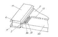
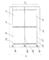
図1は、本発明の実施の形態におけるプリント配線板を示す概略図、図2は、本発明の実施の形態におけるプリント配線板のVカット確認回路部分の詳細を示す図、図3は、本発明の実施の形態におけるプリント配線板のVカット加工後のVカット確認回路部分の詳細を示す図である。図4は、隣接する個別プリント配線板間に形成されたVカット確認回路の詳細を示す図、図5は、本発明の一実施の形態におけるプリント配線板を用いた部品実装工程における搬送時のチャッキング状態を示す部分詳細図、図6は、本発明の他の実施の形態におけるプリント配線板を示す概略図である。
【0024】
図1〜図6において1はプリント配線板、2は個別プリント配線板、3は集合プリント配線板、4,4aは外枠、5,5aはVカット溝、6,6a,6bはVカット加工領域、7は導体回路、8a〜8eはVカット確認回路、9は端子、10はソルダレジスト、11は部品実装装置の搬送用チャッキング部、12はミシン目である。
【0025】
まず本発明のプリント配線板について説明する。
【0026】
図1に示すように、複数の個別プリント配線板2が連結された多数個取りの集合プリント配線板3が両側の外枠4に連結されたプリント配線板1の構成は、外枠4と集合プリント配線板3の間にVカット加工領域6aを有し、隣接する個別プリント配線板間にはVカット加工領域6bを有している。
【0027】
また、Vカット加工領域近傍にはVカット確認回路8a〜8dが形成されている。
【0028】
次に図2を用いてVカット確認回路部分の詳細を説明する。外枠4にVカット確認回路8aの導通検査用の2つの端子9が形成され、両端子間をVカット加工領域6aを介して配線接続され電気的に導通する状態となっている。さらにプリント配線板1の導体回路7を保護するためのソルダレジストと同時形成された絶縁被膜としてのソルダレジスト10が、端子9を除くVカット確認回路上に形成されている。
【0029】
また隣接する個別プリント配線板2間の第2のVカット確認回路8c,8dは、図4(a)に示すように個別プリント配線板2のVカット加工領域6近傍の導体回路7どうしを電気的に連結させたVカット確認回路8cを形成し、その上からソルダレジスト10を形成したものでもよく、あるいは図4(b)に示すような個別プリント配線板2のどの導体回路からも独立したVカット確認回路8dおよび端子9を形成してもよい。
【0030】
上記のプリント配線板をVカット加工した状態を図3に示す。
【0031】
Vカット加工領域6にVカット溝5が形成される際に、Vカット確認回路8aも同時に切削され、断線状態となる。これによりプリント配線板1の完成時の電気検査の際、Vカット確認回路8c,8dの両端子9間の導通検査を行うことにより、Vカット加工の有無も検査できる。このことからVカット加工の忘れを事前に確認することができ、部品実装後のプリント配線板の分割作業を容易に行うことができる。
【0032】
次に、上記のVカット加工を施したプリント配線板1に電子部品を搭載、はんだ付けすることについて説明する。
【0033】
図5に示すように、プリント配線板1は、実装工程において部品実装装置の搬送用チャッキング部11にチャッキング、固定され、電子部品の搭載工程、はんだ付け工程、洗浄工程等へと搬送されていく。このときプリント配線板1のはんだ付けの領域は、個別プリント配線板2が多数個取りに形成された集合プリント配線板3の領域であり、プリント配線板1のチャッキング用の外枠4は、搬送用チャッキング部11に固定されているとともに、全体を覆われ、はんだフロー方式におけるはんだ付けの際に、噴流するはんだが付着しないようになっている。したがってチャッキング用の外枠4に形成された端子9にもはんだが付着しない構造になっている。
【0034】
さらにチャッキングされていない外枠4aのVカット確認回路8aはソルダレジスト10で被覆されているため噴流はんだが付着しない。
【0035】
上記のプリント配線板の部品実装後に電気検査等の工程を経て、個別プリント配線板2に分割され、電子機器に組み込まれていく。このとき外枠4および外枠4aもVカット溝5およびミシン目12の箇所で分割、切り離され産業廃棄物として処理されるが、外枠4,4aにははんだが付着しておらず、容易に処理することが可能となる。
【0036】
また隣接する個別プリント配線板間に形成されたVカット確認回路は、電子回路を構成するプリント配線板としてそのまま電子機器に組み込まれるため、その時点で産業廃棄物となることはない。
【0037】
なお、本発明の実施の形態の説明ではチャッキングされない外枠4aと集合プリント配線板3の分割はミシン目12を介して行う形態としたが、ミシン目12の代わりにVカット溝5aを用いてもよく、その場合のVカット確認回路8eおよび導通検査用の少なくとも2つの端子は、図6に示すようにVカット確認回路8aの端子9と共用し外枠4上に形成することも可能であり、この構成においても部品実装時におけるはんだの付着を防止することが可能であることはいうまでもない。
【0038】
【発明の効果】
以上のように本発明は、従来のVカット確認回路を用いた際に発生するはんだが付着した状態の外枠等の産業廃棄物から、はんだを付着させないVカット確認回路を有するプリント配線板を用いることにより、プリント配線板の製造工程におけるVカット加工の有無を容易に確認でき、かつプリント配線板の実装工程の効率を高めるとともに、電子機器の製造における産業廃棄物も鉛を含有せず、廃棄およびリサイクル処理の容易な、地球環境の保護に有益なプリント配線板を提供することができる。
【図面の簡単な説明】
【図1】 本発明の実施の形態におけるプリント配線板を示す概略図
【図2】 本発明の実施の形態におけるプリント配線板のVカット確認回路部分の詳細を示す図
【図3】 本発明の実施の形態におけるプリント配線板のVカット加工後のVカット確認回路部分の詳細を示す図
【図4】 隣接する個別プリント配線板間に形成されたVカット確認回路の詳細を示す図
【図5】 本発明の実施の形態におけるプリント配線板を用いた部品実装工程における搬送時のチャッキング状態を示す部分詳細図
【図6】 本発明の他の実施の形態におけるプリント配線板のVカット確認回路部分の詳細を示す図
【図7】 従来のプリント配線板を示す概略図
【図8】 従来のプリント配線板のVカット確認回路部分の詳細を示す図
【図9】 従来の隣接する個別プリント配線板間に形成されたVカット確認回路の詳細を示す図
【符号の説明】
1 プリント配線板
2 個別プリント配線板
3 集合プリント配線板
4,4a 外枠
5,5a Vカット溝
6,6a,6b Vカット加工領域
7 導体回路
8a〜8e Vカット確認回路
9 端子
10 ソルダレジスト
11 搬送用チャッキング部
12 ミシン目[0001]
BACKGROUND OF THE INVENTION
The present invention relates to a printed wiring board having a V-cut confirmation circuit for confirming the presence or absence of a V-cut groove provided in order to increase the productivity of component mounting of a printed wiring board used in various electronic devices. .
[0002]
[Prior art]
In recent years, with the progress of cost reduction of various electronic devices, improvement in mass productivity has been demanded also in a mounting process in which electronic components are mounted on a printed wiring board and soldered.
[0003]
Therefore, a mounting method in which individual printed wiring boards are assembled into individual printed wiring boards after mounting and soldering electronic components using a multi-piece collective printed wiring board connected through V-cut grooves and perforations. Has become commonplace.
[0004]
A conventional printed wiring board having a V-cut groove is shown in FIG.
[0005]
In the process of manufacturing the collective printed
[0006]
That is, by conducting a continuity test between the
[0007]
[Problems to be solved by the invention]
The use of the printed
[0008]
Normally, the electronic component is mounted on the printed
[0009]
That is, the
[0010]
Thereafter, the printed wiring board is divided along the V-cut groove and the
[0011]
At this time, the divided
[0012]
However, as one of the protection measures for the global environment in recent years, regulation of lead contained in solder and the flow of reduction and recycling of industrial waste in the process of manufacturing electronic devices are occurring year by year. Since the outer frame portion to be discharged after mounting the board also contains solder, it has been a problem in disposal and recycling processing.
[0013]
The present invention solves the above-mentioned conventional problems, can easily confirm the presence or absence of V-cut processing in the manufacturing process of the printed wiring board, and industrial waste after the mounting of the printed wiring board and manufacturing of the electronic device also contains lead It is an object of the present invention to provide a printed wiring board that constitutes an outer frame part that is easy to dispose or recycle and is useful for protecting the global environment.
[0014]
[Means for Solving the Problems]
In order to solve this problem, the present invention is a printed wiring board having an outer frame and a V-cut groove, wherein at least two terminals are connected to each other via a V-cut processing region, and the V-cut groove is processed. An electronic device is manufactured by mounting an electronic component using a printed wiring board on which an insulating film is formed on the V-cut confirmation circuit in a printed wiring board on which a V-cut confirmation circuit that is electrically disconnected is formed. Thus, the discharge of industrial waste containing lead solder can be eliminated.
[0015]
DETAILED DESCRIPTION OF THE INVENTION
According to the first aspect of the present invention, a chucking outer frame, an unframed outer frame, a V-cut groove, at least two terminals for continuity inspection, and a V-cut machining region between the terminals are provided. And a V-cut confirmation circuit that is electrically disconnected during V-cut groove processing, and an insulating film formed in the V-cut processing region including the V-cut confirmation circuit. The continuity testing terminals are formed on the chucking outer frame, and the V-cut confirmation circuit connected by wiring between the continuity testing terminals is formed on the non-chucked outer frame. The cut confirmation circuit is a printed wiring board that is covered with the insulating film so that the solder does not adhere except for the continuity test terminal. Prevent the deposition of solder on the V-cut confirmation circuit by the presence, with the effect that does not generate industrial waste containing lead solder.
[0016]
The printed wiring board according to claim 1, wherein at least two terminals are formed on the outer frame. By providing at least two inspection terminals on the outer frame, the mounting soldering apparatus in the mounting process is provided. Since the outer frame is not soldered at the chucking portion, the solder does not adhere to the V-cut confirmation circuit including the terminals, and the outer frame can be divided and separated, and can be easily treated as industrial waste that does not contain solder at the time of disposal. It is to become.
[0017]
The invention according to
[0018]
The invention according to
[0019]
Invention of Claim 4 of this invention is a printed wiring board of
[0020]
Invention of
[0021]
The invention according to claim 6 of the present invention is the printed wiring board according to
[0022]
(Embodiment)
Hereinafter, embodiments of the present invention will be described with reference to the drawings.
[0023]
FIG. 1 is a schematic diagram showing a printed wiring board according to an embodiment of the present invention, FIG. 2 is a diagram showing details of a V-cut confirmation circuit portion of the printed wiring board according to the embodiment of the present invention, and FIG. It is a figure which shows the detail of the V cut confirmation circuit part after V cut processing of the printed wiring board in embodiment of invention. FIG. 4 is a diagram showing details of a V-cut confirmation circuit formed between adjacent individual printed wiring boards, and FIG. 5 is a diagram showing a state during conveyance in a component mounting process using the printed wiring board in one embodiment of the present invention. FIG. 6 is a partial detailed view showing a chucking state, and FIG. 6 is a schematic view showing a printed wiring board according to another embodiment of the present invention.
[0024]
1 to 6, 1 is a printed wiring board, 2 is an individual printed wiring board, 3 is a collective printed wiring board, 4 and 4 a are outer frames, 5 and 5 a are V-cut grooves, and 6, 6 a and 6 b are V-cut processing. The region, 7 is a conductor circuit, 8a to 8e are V-cut confirmation circuits, 9 is a terminal, 10 is a solder resist, 11 is a chucking portion for conveying the component mounting apparatus, and 12 is a perforation.
[0025]
First, the printed wiring board of the present invention will be described.
[0026]
As shown in FIG. 1, the configuration of the printed wiring board 1 in which a multi-piece collective printed
[0027]
Further, V cut
[0028]
Next, details of the V-cut confirmation circuit portion will be described with reference to FIG. Two
[0029]
Further, the second V cut
[0030]
FIG. 3 shows a state where the printed wiring board is subjected to V-cut processing.
[0031]
When the V-
[0032]
Next, mounting and soldering of electronic components on the printed wiring board 1 subjected to the V-cut processing will be described.
[0033]
As shown in FIG. 5, the printed wiring board 1 is chucked and fixed to the
[0034]
Furthermore, since the V-
[0035]
After mounting the components of the printed wiring board described above, it is divided into individual printed
[0036]
In addition, the V-cut confirmation circuit formed between the adjacent individual printed wiring boards is incorporated into the electronic device as it is as a printed wiring board constituting the electronic circuit, and does not become industrial waste at that time.
[0037]
In the description of the embodiment of the present invention, the outer frame 4a and the aggregate printed
[0038]
【The invention's effect】
As described above, the present invention provides a printed wiring board having a V-cut confirmation circuit that does not attach solder from an industrial waste such as an outer frame in a state where solder generated when using a conventional V-cut confirmation circuit is attached. By using it, the presence or absence of V-cut processing in the manufacturing process of the printed wiring board can be easily confirmed, and the efficiency of the mounting process of the printed wiring board is increased, and industrial waste in the manufacture of electronic equipment does not contain lead, It is possible to provide a printed wiring board that is easy to dispose and recycle and is useful for protecting the global environment.
[Brief description of the drawings]
FIG. 1 is a schematic diagram showing a printed wiring board according to an embodiment of the present invention. FIG. 2 is a diagram showing details of a V-cut confirmation circuit portion of the printed wiring board according to the embodiment of the present invention. The figure which shows the detail of the V cut confirmation circuit part after V cut processing of the printed wiring board in embodiment. FIG. 4 is the figure which shows the detail of the V cut confirmation circuit formed between adjacent individual printed wiring boards. FIG. 6 is a partial detailed view showing a chucking state during conveyance in a component mounting process using a printed wiring board in an embodiment of the present invention. FIG. 6 is a V-cut confirmation circuit for a printed wiring board in another embodiment of the present invention. FIG. 7 is a schematic diagram showing a conventional printed wiring board. FIG. 8 is a diagram showing details of a V-cut confirmation circuit part of a conventional printed wiring board. FIG. Diagram showing details of the V-cut confirmation circuit formed on preparative wiring plates EXPLANATION OF REFERENCE NUMERALS
DESCRIPTION OF SYMBOLS 1 Printed
Claims (6)
前記Vカット確認回路上を含んだ前記Vカット加工領域に形成された絶縁被膜とを備え、前記導通検査用の端子は前記チャッキング用の外枠上に形成され、
前記導通検査用の端子間を配線接続されたVカット確認回路は前記チャッキングされない外枠上に形成され、
前記Vカット確認回路は前記導通検査用の端子を除いてはんだが付着しないように前記絶縁被膜で被覆されていることを特徴とするプリント配線板。An outer frame for chucking, an outer frame that is not chucked, a V-cut groove, at least two terminals for continuity inspection, and a wiring connection between the terminals via a V-cut processing region, and V-cut groove processing A V-cut confirmation circuit that is electrically disconnected at the time of
An insulating film formed in the V-cut processing region including the V-cut confirmation circuit, and the terminal for continuity inspection is formed on the outer frame for chucking,
A V-cut confirmation circuit wired between the terminals for continuity inspection is formed on the outer frame that is not chucked,
The printed wiring board, wherein the V-cut confirmation circuit is covered with the insulating film so that solder does not adhere except for the terminal for continuity inspection.
Priority Applications (1)
| Application Number | Priority Date | Filing Date | Title |
|---|---|---|---|
| JP15167099A JP4263310B2 (en) | 1999-05-31 | 1999-05-31 | Printed wiring board |
Applications Claiming Priority (1)
| Application Number | Priority Date | Filing Date | Title |
|---|---|---|---|
| JP15167099A JP4263310B2 (en) | 1999-05-31 | 1999-05-31 | Printed wiring board |
Publications (2)
| Publication Number | Publication Date |
|---|---|
| JP2000340899A JP2000340899A (en) | 2000-12-08 |
| JP4263310B2 true JP4263310B2 (en) | 2009-05-13 |
Family
ID=15523682
Family Applications (1)
| Application Number | Title | Priority Date | Filing Date |
|---|---|---|---|
| JP15167099A Expired - Fee Related JP4263310B2 (en) | 1999-05-31 | 1999-05-31 | Printed wiring board |
Country Status (1)
| Country | Link |
|---|---|
| JP (1) | JP4263310B2 (en) |
Families Citing this family (1)
| Publication number | Priority date | Publication date | Assignee | Title |
|---|---|---|---|---|
| JP4906521B2 (en) * | 2007-01-23 | 2012-03-28 | 京セラ株式会社 | Multi-piece wiring board and manufacturing method thereof |
-
1999
- 1999-05-31 JP JP15167099A patent/JP4263310B2/en not_active Expired - Fee Related
Also Published As
| Publication number | Publication date |
|---|---|
| JP2000340899A (en) | 2000-12-08 |
Similar Documents
| Publication | Publication Date | Title |
|---|---|---|
| KR850000216Y1 (en) | Printed circuit board | |
| EP0653905A1 (en) | Direct chip attach module | |
| US6798665B2 (en) | Module and method of manufacturing the module | |
| EP1951012B1 (en) | Method of manufacturing a wiring board including electroplating | |
| US6022466A (en) | Process of plating selective areas on a printed circuit board | |
| KR920007120B1 (en) | Manufacturing method of wiring substrate for surface mounting | |
| JP4263310B2 (en) | Printed wiring board | |
| US6344974B1 (en) | Printed circuit board and method of producing same | |
| JP3770895B2 (en) | Manufacturing method of wiring board using electrolytic plating | |
| JP2001267463A (en) | Semiconductor device substrate and method for manufacturing the same | |
| JP2006100300A (en) | Printed wiring board and manufacturing method therefor | |
| JPH0883819A (en) | Package for tape carrier semiconductor device, its manufacturing method, and manufacture of semiconductor device | |
| JP2009147270A (en) | Method of manufacturing wiring board, wiring board, and semiconductor device | |
| KR101022869B1 (en) | A printed circuit board and method of manufacturing method of the printed circuit board for image sensor module | |
| JPH03165591A (en) | Dip soldering mask | |
| JP2007088232A (en) | Method of manufacturing printed wiring board | |
| JP2004193213A (en) | Tape carrier for tab and method of manufacturing same | |
| JPH09139567A (en) | Surface mounting component mounting pad in printed board and connection structure of through hole for interplayer connection use | |
| JPH0414892A (en) | Structure of solder resist opening of printed-wiring board | |
| JPH11354473A (en) | Semiconductor element substrate and its manufacture | |
| JPH0590764A (en) | Manufacture of electronic component mounting board | |
| KR101109234B1 (en) | A carrier for manufacturing a printed circuit board and a method of manufacturing the same and a method of manufacturing a printed circuit board using the same | |
| JP2003309365A (en) | Flexible compound-type multilayer substrate | |
| JPH0632360B2 (en) | Double-sided connection type flexible circuit board manufacturing method | |
| JPH06296076A (en) | Side face electrode forming method of smd module |
Legal Events
| Date | Code | Title | Description |
|---|---|---|---|
| A621 | Written request for application examination |
Free format text: JAPANESE INTERMEDIATE CODE: A621 Effective date: 20050428 |
|
| A521 | Written amendment |
Free format text: JAPANESE INTERMEDIATE CODE: A821 Effective date: 20050620 |
|
| RD01 | Notification of change of attorney |
Free format text: JAPANESE INTERMEDIATE CODE: A7421 Effective date: 20050620 |
|
| A977 | Report on retrieval |
Free format text: JAPANESE INTERMEDIATE CODE: A971007 Effective date: 20070926 |
|
| A131 | Notification of reasons for refusal |
Free format text: JAPANESE INTERMEDIATE CODE: A131 Effective date: 20071002 |
|
| A521 | Written amendment |
Free format text: JAPANESE INTERMEDIATE CODE: A523 Effective date: 20071130 |
|
| A131 | Notification of reasons for refusal |
Free format text: JAPANESE INTERMEDIATE CODE: A131 Effective date: 20080527 |
|
| A521 | Written amendment |
Free format text: JAPANESE INTERMEDIATE CODE: A523 Effective date: 20080725 |
|
| TRDD | Decision of grant or rejection written | ||
| A01 | Written decision to grant a patent or to grant a registration (utility model) |
Free format text: JAPANESE INTERMEDIATE CODE: A01 Effective date: 20090113 |
|
| A01 | Written decision to grant a patent or to grant a registration (utility model) |
Free format text: JAPANESE INTERMEDIATE CODE: A01 |
|
| A61 | First payment of annual fees (during grant procedure) |
Free format text: JAPANESE INTERMEDIATE CODE: A61 Effective date: 20090212 |
|
| FPAY | Renewal fee payment (event date is renewal date of database) |
Free format text: PAYMENT UNTIL: 20120220 Year of fee payment: 3 |
|
| R150 | Certificate of patent or registration of utility model |
Free format text: JAPANESE INTERMEDIATE CODE: R150 |
|
| FPAY | Renewal fee payment (event date is renewal date of database) |
Free format text: PAYMENT UNTIL: 20130220 Year of fee payment: 4 |
|
| FPAY | Renewal fee payment (event date is renewal date of database) |
Free format text: PAYMENT UNTIL: 20130220 Year of fee payment: 4 |
|
| FPAY | Renewal fee payment (event date is renewal date of database) |
Free format text: PAYMENT UNTIL: 20140220 Year of fee payment: 5 |
|
| R250 | Receipt of annual fees |
Free format text: JAPANESE INTERMEDIATE CODE: R250 |
|
| LAPS | Cancellation because of no payment of annual fees |