JP4250572B2 - Optical scanning device and image forming apparatus using the same - Google Patents
Optical scanning device and image forming apparatus using the same Download PDFInfo
- Publication number
- JP4250572B2 JP4250572B2 JP2004200711A JP2004200711A JP4250572B2 JP 4250572 B2 JP4250572 B2 JP 4250572B2 JP 2004200711 A JP2004200711 A JP 2004200711A JP 2004200711 A JP2004200711 A JP 2004200711A JP 4250572 B2 JP4250572 B2 JP 4250572B2
- Authority
- JP
- Japan
- Prior art keywords
- scanning
- optical
- sub
- optical element
- light
- Prior art date
- Legal status (The legal status is an assumption and is not a legal conclusion. Google has not performed a legal analysis and makes no representation as to the accuracy of the status listed.)
- Expired - Fee Related
Links
Images


Description
本発明は光走査装置及びそれを用いた画像形成装置に関し、特に光源手段から出射した光束を光偏向器としてのポリゴンミラーにより反射偏向させ、走査光学系を介して被走査面上を光走査して画像情報を記録するようにした、例えば電子写真プロセスを有するレーザービームプリンタ(LBP)やデジタル複写機、マルチファンクションプリンタ(多機能プリンタ)等の画像形成装置に好適なものである。 The present invention relates to an optical scanning device and an image forming apparatus using the same, and in particular, a light beam emitted from a light source means is reflected and deflected by a polygon mirror as an optical deflector and optically scanned on a surface to be scanned through a scanning optical system. For example, it is suitable for an image forming apparatus such as a laser beam printer (LBP) having an electrophotographic process, a digital copying machine, or a multi-function printer (multi-function printer) that records image information.
従来よりレーザービームプリンタやデジタル複写機等の画像形成装置においては、例えば半導体レーザから成る光源手段から画像信号に応じて光変調され出射した光束(ビーム)を、例えば回転多面鏡(ポリゴンミラー)より成る光偏向器により周期的に偏向させ、fθ特性を有する走査光学系(走査レンズ系)によって感光性の記録媒体(感光ドラム)面上にスポット状に収束させ、該記録媒体面上を光走査して画像記録を行なっている。 2. Description of the Related Art Conventionally, in an image forming apparatus such as a laser beam printer or a digital copying machine, a light beam (beam) that is light-modulated in accordance with an image signal from a light source means made of, for example, a semiconductor laser, Periodically deflected by an optical deflector, and converged in a spot shape on a photosensitive recording medium (photosensitive drum) surface by a scanning optical system (scanning lens system) having fθ characteristics, and optically scanned on the recording medium surface Image recording.
図15はこの種の従来の画像形成装置に用いられる光走査装置の主走査方向の要部断面図(主走査断面図)である。 FIG. 15 is a sectional view (main scanning sectional view) of the main part in the main scanning direction of an optical scanning device used in this type of conventional image forming apparatus.
同図において半導体レーザを含むレーザユニット91から出射した平行光束は副走査方向にのみ所定の屈折力を有するシリンドリカルレンズ(集光レンズ)92に入射する。シリンドリカルレンズ92に入射した平行光束は主走査断面内においては、そのまま平行光束の状態で出射する。
In the figure, a parallel light beam emitted from a
一方、上記の平行光束は副走査断面内においては集束され、回転多面鏡から成る光偏向器93の偏向面93a近傍に主走査方向に長い線像として結像される。そして、この光偏向器93の偏向面93aで反射偏向された光束はfθ特性を有する走査光学系(fθレンズ系)94によって被走査面である感光ドラム95面上に光スポットとして結像される。そしてこの光スポットによって感光ドラム95面上を繰り返し走査する。走査光学系94は球面レンズ94aとトーリックレンズ94bとから構成されている。
On the other hand, the parallel light beam is focused in the sub-scan section, and is formed as a long line image in the main scanning direction in the vicinity of the
上記の光走査装置においては感光ドラム95面上を光スポットで走査する前に該感光ドラム95面上における画像形成を開始するタイミングを調整するために、光検出器としてのBD(beam detector)センサ−98が設けられている。このBDセンサー98は光偏向器93で反射偏向された光束の一部であるBD光束、即ち感光ドラム95面上の画像形成領域を走査する前の画像形成領域外の領域を走査している時の光束を受光する。このBD光束はBDミラー96で反射され、BDレンズ(集光レンズ)97で集光されてBDセンサー98に入射する。そしてこのBDセンサー98の出力信号からBD信号(同期信号)を検出し、このBD信号に基づいて感光ドラム95面における画像記録の開始タイミングを調整している。
In the optical scanning device described above, a BD (beam detector) sensor as a photodetector is used to adjust the timing for starting image formation on the surface of the
感光ドラム95はレーザユニット91内の半導体レーザの駆動信号に同期して一定速度で回転し、感光ドラム95面は走査される光スポットに対して副走査方向に移動する。
The
このようにして感光ドラム95上に静電潜像が形成される。この静電潜像は周知の電子写真プロセスによって現像され、紙などの被転写材に転写されて画像が具現化される。
In this way, an electrostatic latent image is formed on the
また走査光学系を使用した多重画像形成装置は一般に複数の画像形成部において異なった色の画像を形成し、例えば搬送ベルトの如き搬送手段によって紙を搬送し、この紙上に画像を重ねて転写し画像形成を行なう。特に多色現像を行なうフルカラー画像を得る場合は、わずかな重なりずれでも画像を悪化させる。例えば400dpiであれば1画素63.5μmの数分の1の重なりずれでさえ、色ずれや色見ずれの変化として現われ画像を著しく悪化させる。 In addition, a multiple image forming apparatus using a scanning optical system generally forms images of different colors in a plurality of image forming units, conveys paper by a conveying means such as a conveying belt, and transfers the image on this paper in an overlapping manner. Image formation is performed. In particular, when obtaining a full-color image to be subjected to multicolor development, the image is deteriorated even by a slight overlap shift. For example, if it is 400 dpi, even an overlap shift of a fraction of 63.5 μm per pixel appears as a change in color shift or color shift, and the image is remarkably deteriorated.
従来はこれに対し同一の走査光学系を用いて色現像を行なう、即ち同じ光学特性で光走査し、画像のずれを緩和していた。しかしながらこの方法では多重画像やフルカラーを出力するのに時間がかかるという問題点があった。この問題点を解決するために各色の画像を得るために別々の光走査装置で画像を形成し、搬送部によって送られる紙上で画像を重ね合わせるという方法がある。 Conventionally, color development is performed by using the same scanning optical system, that is, optical scanning is performed with the same optical characteristics to reduce image shift. However, this method has a problem that it takes time to output multiple images and full colors. In order to solve this problem, there is a method in which images are formed by separate optical scanning devices in order to obtain an image of each color, and the images are superimposed on the paper fed by the transport unit.
しかしながらこのとき懸念されることとしては画像を重ね合わせるときの色ずれである。これに対して有効な方法として画像の位置を検出し、検出信号にしたがって画像を補正すべく画像形成部を制御するという方法がある(例えば特許文献1参照)。 However, a concern at this time is color misregistration when images are superimposed. On the other hand, as an effective method, there is a method of detecting the position of the image and controlling the image forming unit to correct the image according to the detection signal (see, for example, Patent Document 1).
一方、複数の感光体にビームを走査する画像形成装置においては、複数の感光体上に潜像を形成するために通常は感光体と同じ数の走査光学系が用いられている。この問題点としては走査光学系の数だけ光学部品が必要になり、特に光偏向器(ポリゴンミラー)は高価であるためにコスト高となるといった問題点がある。また特に高速で高精細な走査光学系の場合には光偏向器が大きくなると同時に高速に偏向させる能力を有する必要があるためにさらに問題は深刻となる。 On the other hand, in an image forming apparatus that scans a plurality of photosensitive members with beams, the same number of scanning optical systems as that of the photosensitive members are usually used to form latent images on the plurality of photosensitive members. As this problem, the number of optical components is required as many as the number of scanning optical systems. In particular, the optical deflector (polygon mirror) is expensive, and therefore the cost is high. In particular, in the case of a high-speed and high-definition scanning optical system, the problem becomes more serious because the optical deflector needs to have the ability to deflect at high speed at the same time.
この問題に対応するために複数のビームを共通の光偏向器で偏向する光走査装置が提案されている。また共通の光偏向器で副走査方向の感光体を走査する光走査装置においては、副走査方向の画像の重ね合わせの精度を向上させるために副走査方向のビームの描画位置をずらす機構を有する必要がある。この方法としては副走査方向のビームの描画開始を行う光偏向器の偏向面を選択することにより副走査方向に1ラインずつ描画位置をずらすことで調整を行っていた。 In order to cope with this problem, an optical scanning device that deflects a plurality of beams with a common optical deflector has been proposed. An optical scanning device that scans a photoconductor in the sub-scanning direction with a common optical deflector has a mechanism for shifting the drawing position of the beam in the sub-scanning direction in order to improve the accuracy of superimposing images in the sub-scanning direction. There is a need. In this method, adjustment is performed by selecting a deflection surface of an optical deflector that starts drawing of a beam in the sub-scanning direction and shifting the drawing position by one line in the sub-scanning direction.
さらに最近は、コンパクトで低価格で光画質なフルカラーの画像形成装置が求められており、この要求を満たす1つの方法として、単一の共通ポリゴンを使用して複数のビームを走査することにより部品点数を減らすことでコストダウンを行なう系が提案されている。
しかしながら、共通のポリゴンミラーを使用する場合に複数ビームを異なる被走査面に各々導くためには光路の分離が必要である。このため副走査方向のビームの距離を離しておく必要があり、この結果、該ポリゴンミラーが厚くなりコストアップとなるという問題点があった。 However, when a common polygon mirror is used, it is necessary to separate optical paths in order to guide a plurality of beams to different scanning surfaces. Therefore, it is necessary to keep the beam distance in the sub-scanning direction. As a result, there is a problem that the polygon mirror becomes thick and the cost increases.
また走査光学系の第1の光学素子(走査レンズ)を共通化することでコストダウンを図ってもレンズの光線通過位置が副走査方向に離れた位置を通過するために、該レンズの副走査方向の高さが大きくなり、この結果、大きなコストダウンの効果が少ないという問題点もあった。 Even if the first optical element (scanning lens) of the scanning optical system is used in common, even if the cost is reduced, the light beam passing position of the lens passes through a position separated in the sub-scanning direction. The height of the direction is increased, and as a result, there is a problem that the effect of a large cost reduction is small.
本発明は光偏向器の厚みを薄くすると共に被走査面上における走査線曲がりを小さく抑え良好なる光学性能が得られる簡易でコンパクトな構成の光走査装置及びそれを用いた画像形成装置の提供を目的とする。 The present invention provides an optical scanning device having a simple and compact configuration capable of reducing the thickness of the optical deflector and suppressing scanning line bending on the surface to be scanned to obtain good optical performance, and an image forming apparatus using the optical scanning device. Objective.
上記の問題を解決するために、本発明では、複数の光源手段と、前記複数の光源手段から発した複数の光束を偏向する光偏向器と、前記光偏向器の同一の偏向面によって偏向された複数の光束を各々異なる被走査面上に結像させる走査光学系と、を有する光走査装置であって、
前記光偏向器の同一の偏向面に入射する複数の光束は、副走査断面内において前記光偏向器の偏向面の法線に対して異なる角度を持って入射し、
前記走査光学系は、前記光偏向器の同一の偏向面にて偏向された複数の光束について共通に使用される第1の光学素子と前記第1の光学素子と前記被走査面との間に配置され且つ前記複数の光束の各々に対して配置された第2の光学素子とを有し、
前記第1の光学素子と前記第2の光学素子の主走査断面内のパワーを各々φ1m、φ2m、前記第1の光学素子と前記第2の光学素子の副走査断面内のパワーを各々φ1s、φ2sとするとき、
|φ1m/φ2m|>2.0
0≦|φ1s|<0.001
|φ1s/φ2s|<0.1
を満足し、
副走査断面内において、前記第2の光学素子に入射する光線の主光線は、前記第2の光学素子の副走査断面内の光軸に対して角度を有し、且つ、
副走査断面内において、前記第2の光学素子の光軸は、前記第2の光学素子に入射する光線の副走査断面内の主光線位置よりも偏向反射点側に偏心し、且つ、
前記第2の光学素子は、光入射面又は光出射面のうち1以上が主走査断面内において球面形状であり、且つ、前記第2の光学素子は、副走査断面内において軸上のパワーに対して軸外のパワーが弱い形状である構成とした。
In order to solve the above problems, in the present invention, a plurality of light source means, an optical deflector for deflecting a plurality of light beams emitted from the plurality of light source means, and the same deflecting surface of the optical deflector are deflected. A scanning optical system that forms an image of the plurality of light beams on different scanned surfaces,
A plurality of light beams incident on the same deflection surface of the optical deflector are incident at different angles with respect to the normal line of the deflection surface of the optical deflector in the sub-scan section,
The scanning optical system includes a first optical element that is commonly used for a plurality of light beams deflected by the same deflecting surface of the optical deflector, the first optical element, and the scanned surface. A second optical element disposed and disposed with respect to each of the plurality of light beams,
The power in the main scanning section of the first optical element and the second optical element is φ1m and φ2m, respectively, and the power in the sub-scanning section of the first optical element and the second optical element is φ1s, respectively. When φ2s
| Φ1m / φ2m |> 2.0
0 ≦ | φ1s | <0.001
| Φ1s / φ2s | <0.1
Satisfied,
In the sub-scan section, the principal ray of the light beam incident on the second optical element has an angle with respect to the optical axis in the sub-scan section of the second optical element, and
In the sub-scan section, the optical axis of the second optical element is decentered toward the deflection reflection point side with respect to the principal ray position in the sub-scan section of the light beam incident on the second optical element , and
In the second optical element, at least one of the light incident surface and the light emitting surface has a spherical shape in the main scanning section, and the second optical element has an axial power in the sub-scanning section. On the other hand, the configuration is such that the off-axis power is weak.
本発明によれば前述の如く走査光学系を構成する第1の光学素子の副走査断面内での屈折力を略ノンパワーに設定することにより、光偏向器の厚みを薄くでき、また走査線曲がりを抑えた良好なる光学性能を得ることができる簡易でコンパクトな構成の光走査装置及びそれを用いた画像形成装置を達成することができる。 According to the present invention, the thickness of the optical deflector can be reduced by setting the refractive power in the sub-scan section of the first optical element constituting the scanning optical system to substantially non-power as described above, and the scanning line. It is possible to achieve an optical scanning device having a simple and compact configuration capable of obtaining good optical performance with curving and an image forming apparatus using the same.
[実施形態1]
図1は本発明の実施形態1の光走査装置(画像形成装置)の副走査方向の要部断面図(副走査断面図)である。
[Embodiment 1]
FIG. 1 is a cross-sectional view (sub-scanning cross-sectional view) of the main part in the sub-scanning direction of the optical scanning device (image forming apparatus) according to the first embodiment of the present invention.
ここで、主走査方向とは光偏向器の回転軸及び走査光学系の光軸に垂直な方向(光偏向器で光束が反射偏向(偏向走査)される方向)を示し、副走査方向とは光偏向器の回転軸と平行な方向を示す。また主走査断面とは主走査方向に平行で走査光学系の光軸を含む平面を示す。また副走査断面とは主走査断面と垂直な断面を示す。 Here, the main scanning direction is a direction perpendicular to the rotation axis of the optical deflector and the optical axis of the scanning optical system (the direction in which the light beam is reflected and deflected (deflected and scanned) by the optical deflector), and the sub-scanning direction is The direction parallel to the rotation axis of the optical deflector is shown. The main scanning section indicates a plane parallel to the main scanning direction and including the optical axis of the scanning optical system. The sub-scanning cross section indicates a cross section perpendicular to the main scanning cross section.
本実施形態において画像信号に応じて変調された光束を複数発する光源手段からの光束は2つの走査グループ(走査光学系)S1,S2に分割されている。この2つの走査グループS1,S2は光偏向器(ポリゴンミラー)1に対して左右対称で構成されており、該2つの走査グループS1,S2の光学的作用は同一の為、以下図面上、右半分の走査グループS1に対して説明する。 In the present embodiment, the light beam from the light source means that emits a plurality of light beams modulated according to the image signal is divided into two scanning groups (scanning optical systems) S1 and S2. The two scanning groups S1 and S2 are configured symmetrically with respect to the optical deflector (polygon mirror) 1, and the optical actions of the two scanning groups S1 and S2 are the same. The half scan group S1 will be described.
図中、6M、6Yは感光ドラムであり、導電体に感光層が塗布されており、光学箱9に収納された走査光学部から射出された光束により静電潜像を形成している。
In the figure,
1は光偏向器であり、例えばポリゴンミラー(回転多面鏡)より成っており、モータ等の駆動手段(不図示)により一定速度で回転している。 An optical deflector 1 is composed of, for example, a polygon mirror (rotating polygonal mirror), and is rotated at a constant speed by a driving means (not shown) such as a motor.
本実施形態では副走査断面内に各要素と各光束を投影したとき、2つの光束は、ポリゴンミラー1の偏向面の法線に対して異なる入射角度で斜入射してい
る(斜入射走査光学系)。
In this embodiment, when each element and each light beam are projected in the sub-scan section, the two light beams are incident obliquely at different incident angles with respect to the normal line of the deflection surface of the polygon mirror 1 (oblique incident scanning optics). system).
また、ポリゴン偏向面への入射角度は±Θの絶対値が同じで符号が異なる角度で入射させているが、|Θ1|≠|Θ2|と言った2つの異なる絶対値を有した角度Θ1とΘ2で有っても良い。 The incident angle to the polygon deflection surface is the same as the angle θ1 having two different absolute values such as | Θ1 | ≠ | Θ2 | It may be Θ2.
また、本実施形態では、ポリゴンミラー1の同一の偏向面に2本の光束が入射している形態を取っているが、3本以上の光束が入射している形態でも良い。 In the present embodiment, two light beams are incident on the same deflection surface of the polygon mirror 1, but three or more light beams may be incident.
2Aは第1の光学素子としての第1の走査レンズであり、副走査断面内において屈折力(パワー)がノンパワー、主走査断面内において屈折力(パワー)を有している。第1の走査レンズ2Aは副走査断面内において光入射面と光出射面の曲率半径が等しい面を有し、主走査断面において非球面形状の面を1以上含んでいる。この第1の走査レンズ2Aは入射した光束に対し主に主走査方向の結像及び等速走査(fθ特性)を担当することになる。
第2の光学素子3M、3Yは、本実施形態において走査レンズを用いるが、回折素子や曲面ミラーに置換しても良い。また、第2の光学素子は、本実施形態において以下のように1枚の走査レンズで構成されているが、2枚以上の走査レンズで構成されていても良い。
The second
第1の光学素子2Aは、本実施形態において走査レンズを用いるが、回折素子や曲面ミラーに置換しても良い。
The first
3M、3Yは各々第2の光学素子としての第2の走査レンズであり、光入射面が主走査断面内において球面形状であり、光出射面が主走査断面内において変曲点を有しない形状であり、副走査断面内において走査軸上に対して軸外の屈折力が弱いプラスチック材より成っている。
第2の光学素子としての第2の走査レンズは、回折素子や曲面ミラーでも良い。 The second scanning lens as the second optical element may be a diffraction element or a curved mirror.
また第2の走査レンズ3M、3Yの各々の副走査断面内の光軸は、該第2の走査レンズ3M、3Yに入射する光線の副走査断面内の主光線位置よりも偏心している。また第2の走査レンズ3M、3Yは各々副走査断面内において軸上と軸外の倍率が略一定となるように設定されている。この第2の走査レンズ3M、3Yは入射した光束に対し主に副走査方向の像面湾曲の補正を担当することになる。
Further, the optical axes in the sub-scanning sections of the
本実施形態では第1の走査レンズ2Aと第2の走査レンズ3Mで第1の走査レンズ系を構成しており、また第1の走査レンズ2Aと第2の走査レンズ3Yで第2の走査レンズ系を構成しており、また第1、第2の走査レンズ系で走査光学系を構成している。本実施形態では走査光学系の副走査断面内の結像倍率が1.3倍以下と成るように設定している。
In the present embodiment, the first scanning lens system is constituted by the
第1、第2の走査レンズ系は各々ポリゴンミラー1によって反射偏向された画像情報に基づく光束E1,E2を被走査面としての感光ドラム6M,6Y面上に結像させ、かつ副走査断面内においてポリゴンミラー1の偏向面と感光ドラム6M,6Y面上との間を共役関係にすることにより、倒れ補正機能を有している。
The first and second scanning lens systems each form light beams E1 and E2 based on image information reflected and deflected by the polygon mirror 1 on the
4A,5Mは各々順に第1、第2の折り返しミラー(光学部材)であり、光束E1の光路中に設けられており、光束を所定の方向へ反射させている。5Yは第3の折り返しミラー(光学部材)であり、光束E2の光路中に設けられており、光束を所定の方向へ反射させている。
これら第1、第2、第3の折り返しミラーは後述するように移動可能又は/及び変形可能に構成されており、調整部材により被走査面上における走査線曲がり調整している。 These first, second, and third folding mirrors are configured to be movable or / and deformable as will be described later, and the scanning line bending is adjusted on the surface to be scanned by the adjusting member.
本実施形態において副走査断面内に各要素と各光束を投影したとき、第1の折り返しミラー4Aはポリゴンミラー1で偏向された2つの光束E1,E2を2つの光路に分離しており、また入射光束E1を感光ドラム6M,6Yと反対側に反射させている。9は光学箱であり、走査光学部の各部品を格納している。
In this embodiment, when each element and each light beam are projected in the sub-scan section, the
本実施形態では感光ドラムの下部に走査光学部を配置しており、該走査光学部は1つのポリゴンミラー1に対して両側にそれぞれ2本の光束を入射させ、各々の対応する感光ドラム面上に光束E1〜E4を導光して、カラー画像を高速に印字している。 In the present embodiment, a scanning optical unit is disposed below the photosensitive drum, and the scanning optical unit causes two light beams to enter the polygon mirror 1 on both sides, respectively, on each corresponding photosensitive drum surface. Light beams E1 to E4 are guided to color images at high speed.
本実施形態における走査光学系は上記の如く副走査断面内で斜入射走査光学系である。斜入射走査光学系とは副走査断面(紙面に対して平行な面)内で、ポリゴンミラー1の回転軸に垂直な面(主走査断面)に対し斜め方向から光束を入射させる光学系である。このように斜め入射させることで、ポリゴンミラー1の副走査方向の偏向反射面の幅を狭く取ることが可能となる。また第1の走査レンズ2Aは同様に副走査方向のそれぞれの光束の位置が近いために、副走査方向の幅を狭くできる。
The scanning optical system in this embodiment is an oblique incidence scanning optical system in the sub-scan section as described above. The oblique incidence scanning optical system is an optical system in which a light beam is incident from an oblique direction with respect to a surface (main scanning section) perpendicular to the rotation axis of the polygon mirror 1 in a sub-scanning section (plane parallel to the paper surface). . Such oblique incidence makes it possible to reduce the width of the deflecting / reflecting surface of the polygon mirror 1 in the sub-scanning direction. Similarly, since the
次に本実施形態の光学的作用について説明する。 Next, the optical action of this embodiment will be described.
本実施形態において、後述する2つの入射光学系からポリゴンミラー1の偏向面に入射した2つの光束E1,E2は主走査断面内に対して角度±θをもって反射され、偏向走査される。その後、2つの光束E1,E2は共通の第1の走査レンズ2Aに入射する。第1の走査レンズ2Aを通過した2つの光束E1,E2は第1の折り返しミラー4Aにより各光路に分離される。第1の折り返しミラー4Aによって反射された光束E1は第2の走査レンズ3Mを通過後、第2の折り返しミラー5Mによって図面上、上方に反射し、空間内で自身の光路と交差する。第1、第2の折り返しミラー4A,5Mで折り返されることで別の光束E2の光路と2回交差して感光ドラム6Mに達する。
In the present embodiment, two light beams E1 and E2 incident on the deflecting surface of the polygon mirror 1 from two incident optical systems to be described later are reflected at an angle ± θ with respect to the main scanning section and deflected and scanned. Thereafter, the two light beams E1 and E2 are incident on the common
一方、光束E2の光路では第1の走査レンズ2Aを通過した光束E2は第1の折り返しミラー4Aの脇を通過し、光束E1と光路が分離される。そして光束E2は第2の走査レンズ3Yを通過後、第3の折り返しミラー5Yによって図面上、上方に反射し、感光ドラム6Yに達する。
On the other hand, in the optical path of the light beam E2, the light beam E2 that has passed through the
そして感光ドラム6C、6Kに向かう光束は同様に静電潜像を形成し、不図示の現像、転写、定着の電子写真プロセスにおり紙上に多色画像を形成する。 The light fluxes directed to the photosensitive drums 6C and 6K similarly form an electrostatic latent image, and form a multicolor image on paper in an unillustrated electrophotographic process of development, transfer, and fixing.
本実施形態における第1の走査レンズ2Aは2つの光束E1,E2で共用され、第2の走査レンズ3M、3Yは光束E1,E2にそれぞれ用いられる。
In the present embodiment, the
図2は図1に示した一方の走査グループ(走査光学系)S1の主走査方向の要部断面図(主走査断面図)、図3Aは図2の副走査方向の要部断面図(副走査断面図)である。図2、図3Aにおいて図1に示した要素と同一要素には同符番を付している。尚、折り返しミラーは省略して示している。 2 is a sectional view (main scanning sectional view) of the main scanning direction of one scanning group (scanning optical system) S1 shown in FIG. 1, and FIG. FIG. 2 and 3A, the same elements as those shown in FIG. 1 are denoted by the same reference numerals. Note that the folding mirror is omitted.
また、図3Aは図1におけるマゼンタステーション(M)のみを示しており,イエローステーション(Y)は省略している。なお、イエローステーションに付いては偏向反射面の法線31に対して線対称な配置の光学系になっている。 FIG. 3A shows only the magenta station (M) in FIG. 1, and the yellow station (Y) is omitted. Note that the yellow station is an optical system arranged symmetrically with respect to the normal 31 of the deflecting / reflecting surface.
図中、11は画像信号に応じて変調された光束を発する複数の光源手段であり、例えば半導体レーザ等より成っている。尚、本実施形態では複数の光源手段より構成しているが、これに限らず、例えば複数の発光部を有する光源手段より構成しても良い。12は変換光学素子(例えばコリメーターレンズ等)であり、複数の光源手段11から発した光束を略平行光束(もしくは略発散光束もしくは略収束光束)に変換している。13は開口絞りであり、複数の通過光束を制限してビーム形状を整形している。14は集光レンズとしてのシリンドリカルレンズであり、副走査方向にのみ所定の屈折力(パワー)を有しており、開口絞り13を通過した複数の光束を副走査断面内で後述するポリゴンミラー1の偏向面1aの近傍にほぼ線像として一旦結像させている。尚、コリメーターレンズ12、開口絞り13、そしてシリンドリカルレンズ14等の各要素は入射光学系の一要素を構成している。
In the figure,
7は走査レンズ系であり、上述した形状より成る第1の走査レンズ2(2A)と、第2の走査レンズ3(3M,3Y)より成り、ポリゴンミラー1によって反射偏向された画像情報に基づく複数の光束を被走査面としての異なる感光ドラム面6(6M,6Y)上に結像させ、かつ副走査断面内においてポリゴンミラー1の偏向面1aと感光ドラム面6との間を共役関係にすることにより、倒れ補正機能を有している。
A
6(6M,6Y)は被走査面としての感光ドラム面、15はポリゴンミラー1により偏向走査される走査光である。 Reference numeral 6 (6M, 6Y) denotes a photosensitive drum surface as a surface to be scanned, and 15 denotes scanning light deflected and scanned by the polygon mirror 1.
図3Aにおいて31は偏向面1aの偏向反射点36における法線である。33は第2の走査レンズ3の光軸であり、光線通過位置34に対して偏向面1aの偏向反射点36側に偏心している。光線通過位置34は光束の主光線に相当している。光軸33は偏向面1aの法線31に対して平行である。
In FIG. 3A, 31 is a normal line at the
本実施形態では副走査断面内においてシリンドリカルレンズ14からの複数の光束は偏向面1aの法線31に対して角度αを持って入射する。このため第2の走査レンズ3に入射する走査線は曲がった状態で入射し、感光ドラム面上においても走査線曲がりが発生し易い。このため走査線曲がりの発生を抑える必要があり、走査光学系7を副走査断面内で結像倍率が1.3倍以下と成るようにして走査線曲がりが発生しないようにしている。すなわち走査光学系の製造上の走査線曲がりの主要な発生要因である第2の走査レンズの子線光軸高さの主走査方向位置による変化の影響を小さく抑えている。このとき第2の走査レンズ3を偏心(平行偏心又は/及び回転偏心)させることによって、副走査断面内の結像倍率が1.3倍以下で感光ドラム上のスポット回転と走査線曲がりを除去することを容易にしている。
In the present embodiment, a plurality of light beams from the
即ち、本実施形態では第2の走査レンズ3の光軸33を光線通過位置(主光線位置)34に対して偏向面1aの偏向反射点36側に偏心させ、それと同時に第2の走査レンズ3に入射する光束の主光線34を副走査断面内において、光軸33に対して角度を有して入射させている。
That is, in this embodiment, the
図3Bは本発明の入社光学系の説明図である。図において、11Y、11Mは光源、12Y,12Mはコリメータレンズ、13Y、13Mは絞り、14Y,14Mはシリンドリカルレンズである。なお,シアンステーションとブラックステーションはポリゴン回転軸に対称に同じ光学系を配置している。 FIG. 3B is an explanatory diagram of the in-company optical system of the present invention. In the figure, 11Y and 11M are light sources, 12Y and 12M are collimator lenses, 13Y and 13M are diaphragms, and 14Y and 14M are cylindrical lenses. The cyan station and black station have the same optical system arranged symmetrically with respect to the polygon rotation axis.
図においては、光源11Y、11Mをそれぞれ出射したレーザ光束はコリメータレンズ12Y,12Mにより屈折され平行光束として副走査方向にパワーを有するシリンドリカルレンズ14Y,14Mに入射する。シリンドリカルレンズ14Y,12Mにおいては副走査方向に集光され絞り13Y,13Mにより光束幅が規制された後に、ポリゴンミラーの偏向反射面に角度+ΘとマイナスΘという異なる入射角度で入射する。
In the figure, the laser beams emitted from the light sources 11Y and 11M are refracted by the
図4は本発明を実施しなかった場合のポリゴンミラーの偏向面近傍の光線の状態を示した副走査断面図である。 FIG. 4 is a sub-scan sectional view showing the state of light rays in the vicinity of the deflection surface of the polygon mirror when the present invention is not carried out.
同図において41はポリゴンミラー、42は第1の走査レンズ、43は偏向反射面の副走査断面内における法線、44は偏向面で反射された後の第1の走査光、45は偏向面で反射された後の第2の走査光、47、48は各々第2の走査レンズ、49(49M,49Y)は被走査面(感光ドラム面)である。 In the figure, 41 is a polygon mirror, 42 is a first scanning lens, 43 is a normal line in the sub-scan section of the deflecting reflecting surface, 44 is the first scanning light after being reflected by the deflecting surface, and 45 is the deflecting surface. The second scanning light 47 and 48 after being reflected by the second scanning lens 47 and 48 are second scanning lenses, and 49 (49M and 49Y) are scanned surfaces (photosensitive drum surfaces).
同図に示した第1の走査レンズ42は副走査断面内において両凸形状で正のパワーを有している。この第1の走査レンズ42が破線で示したように製造誤差により法線43より上方に偏心して配置された場合には第1の走査光44は屈折され設計値からずれた位置を通過する。この光線のシフト量は主走査方向の像高により変化し、主走査方向の像高が高い方がよりシフト量が大きくなる。 The first scanning lens 42 shown in the figure has a positive power with a biconvex shape in the sub-scan section. When the first scanning lens 42 is arranged eccentrically above the normal line 43 due to a manufacturing error as indicated by a broken line, the first scanning light 44 is refracted and passes a position deviated from the design value. The amount of shift of the light beam varies depending on the image height in the main scanning direction, and the shift amount becomes larger as the image height in the main scanning direction is higher.
従って第2の走査レンズ47には設計基準の光線よりU字型の軌跡を描いた光線が入射し、この結果、被走査面49上においては凸形状をした走査線が形成される。同様に第2の走査光45も屈折され設計値からずれた位置を通過することで、結果として被走査面49上においては凸形状をした走査線が形成される。 Therefore, a light beam having a U-shaped locus from the design reference light beam is incident on the second scanning lens 47, and as a result, a convex scanning line is formed on the surface to be scanned 49. Similarly, the second scanning light 45 is also refracted and passes through a position deviated from the design value. As a result, a scanning line having a convex shape is formed on the scanned surface 49.
図5は本発明を実施した場合のポリゴンミラーの偏向面近傍の光線の状態を示した副走査断面図である。同図において図1に示した要素と同一要素には同符番を付している。 FIG. 5 is a sub-scan sectional view showing the state of light rays near the deflection surface of the polygon mirror when the present invention is implemented. In the figure, the same elements as those shown in FIG.
同図において53は偏向面の副走査断面内における法線、54は偏向反射面で反射された後の第1の走査光、55は偏向面で反射された後の第2の走査光、33は各々第2の走査レンズ3M,3Yの光軸である。
In the figure, 53 is a normal line in the sub-scan section of the deflection surface, 54 is the first scanning light after being reflected by the deflection reflection surface, 55 is the second scanning light after being reflected by the deflection surface, 33 Are the optical axes of the
同図に示したように第1の走査レンズ2Aの副走査断面内の両レンズ面は緩い曲率半径(同一の曲率半径)で構成されており、即ち略ノンパワーで構成されている。
As shown in the figure, both lens surfaces in the sub-scan section of the
即ち、本実施形態では第1の走査レンズ2Aの副走査断面内の屈折力をφ1sとするとき、
0≦|φ1s|<0.001 ‥‥(1)
を満足するように形成している。
That is, in this embodiment, when the refractive power in the sub-scanning section of the
0 ≦ | φ1s | <0.001 (1)
It is formed to satisfy.
また本実施形態においては第1の走査レンズ2Aと第2の走査レンズ(3M、3Y)の主走査断面内の屈折力を各々φ1m、φ2mとするとき、
|φ1m/φ2m|>2.0 ‥‥(2)
を満足するように構成している。
In this embodiment, when the refractive powers in the main scanning section of the
| Φ1m / φ2m |> 2.0 (2)
It is configured to satisfy.
条件式(1)は第1の走査レンズ2Aの副走査断面内の屈折力を規定したものであり、条件式(1)を外れると第1の走査レンズ2Aが副走査断面内でパワーを持つ事になり、ポリゴンの回転角度によって副走査方向に屈折される量が変化するため走査線曲がりの発生に寄与する。従ってレンズの配置誤差等によりレンズの位置が変化した場合に走査線曲がりが発生することになり、光走査装置の製造上走査線曲がりが大きくなり良くない。
Conditional expression (1) defines the refractive power in the sub-scanning section of the
条件式(2)は第1の走査レンズ2Aと第2の走査レンズの主走査断面内での屈折力の比に関するものであり、条件式(2)を外れると第2の走査レンズの主走査断面におけるパワーが大きくなりfθ特性を良好な性能にするために主走査断面における屈折力を画角に応じて変化させる必要がある。これにより第2の走査レンズの主走査断面における形状がうねった形状となり易い。レンズ形状のうねりはレンズ配置誤差などが発生すると走査線がうねった形状となり、他の光学部材によって走査線曲がりを補正しても一様な曲がりは補正できてもうねりを補正する事が出来ないため良くない。
Conditional expression (2) relates to the ratio of refractive power in the main scanning section of the
更に好ましくは上記条件式(1)、(2)を、
0≦|φ1s|<0.0001 ‥‥(1a)
|φ1m/φ2m|>4.0 ‥‥(2a)
とするのが良い。
More preferably, the conditional expressions (1) and (2) are
0 ≦ | φ1s | <0.0001 (1a)
| Φ1m / φ2m |> 4.0 (2a)
It is good to do.
本実施形態では製造誤差等により第1の走査レンズ2Aが副走査方向にシフトして配置されても、副走査断面内の光線の位置はほとんど変化しないために、第2の走査レンズ3M、3Yに入射する光線の状態は変化しない。従って走査光の曲がりは発生しないため、製造誤差による走査線の曲がり発生の大きな要因であるレンズ及びレンズ面のシフトについて鈍感な光学系とすることができ、この結果色ズレを小さく抑えることが可能となる。
In the present embodiment, even if the
図6は本発明を実施しなかったときの第2の走査レンズ(47,48)の主走査断面内での形状を示した説明図である。 FIG. 6 is an explanatory view showing the shape of the second scanning lens (47, 48) in the main scanning section when the present invention is not carried out.
同図において62は第2の走査レンズ(47,48)の入射側のレンズ面、63は出射側のレンズ面、64は第2の走査レンズ47,48の主走査断面内での光軸である。 In this figure, 62 is the lens surface on the incident side of the second scanning lens (47, 48), 63 is the lens surface on the exit side, and 64 is the optical axis in the main scanning section of the second scanning lens 47, 48. is there.
前記条件式(2)、(2a)を満たさないと、走査光学系のfθ特性を補正するために第2の走査レンズ(47,48)の形状をうねらせた形状とする必要がある。 If the conditional expressions (2) and (2a) are not satisfied, it is necessary to make the shape of the second scanning lens (47, 48) undulate in order to correct the fθ characteristic of the scanning optical system.
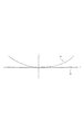
この走査レンズが製造誤差等により副走査方向の配置に狂いがあった場合の走査光の被走査面上における光線到達位置を図7に示す。図7は従来の走査光学系による走査線曲がりを示したグラフである。 FIG. 7 shows the light beam arrival position on the surface to be scanned when the scanning lens is misaligned in the sub-scanning direction due to a manufacturing error or the like. FIG. 7 is a graph showing scanning line bending by a conventional scanning optical system.
同図において横軸Yが描画位置(像高)、縦軸Zが副走査方向の光線到達位置を示している。71は第2の走査レンズ(47,48)が傾いて配置された場合の副走査断面内での走査位置を示したグラフである。グラフ71に示したように副走査断面内の走査位置は描画位置によりうねった形状となり、これはレンズ形状に起因している。このとき後述する如く走査線曲がり調整を行なった場合の走査線の補正量を示したものがグラフ72である。
In the figure, the horizontal axis Y indicates the drawing position (image height), and the vertical axis Z indicates the light beam arrival position in the sub-scanning direction.
通常、走査線曲がり調整により第2の走査レンズ(47,48)以外の光学部材を変形又は変位させた場合には、走査線の補正量はうねりのない軌跡を示す。従って走査線曲がり調整を行なってもグラフ72のラインのように走査線のうねりが残ってしまう。
Normally, when an optical member other than the second scanning lens (47, 48) is deformed or displaced by scanning line bending adjustment, the scanning line correction amount shows a locus without waviness. Therefore, even if the scanning line bending adjustment is performed, the undulation of the scanning line remains as in the line of the
また仮に第2の走査レンズ(47,48)の傾きで走査線曲がり調整を行なう場合においても、該第2の走査レンズ(47,48)により発生したうねり成分は調整可能であるが、他の要因で発生した曲がり形状(例えばポリゴンミラーのうなずき等)で発生する曲がり形状はうねりのない形状であるため、結果としてうねり成分が大きくなり重ね合わせ画像の色ずれを悪化させる。 In addition, even when the scanning line bending adjustment is performed by the inclination of the second scanning lens (47, 48), the swell component generated by the second scanning lens (47, 48) can be adjusted. Since the bend shape generated by the factor (for example, the nod of the polygon mirror) is a shape having no undulation, the undulation component becomes large as a result, and the color shift of the superimposed image is deteriorated.
図8は本発明を用いた場合の第2の走査レンズの主走査断面内での形状を示した説明図である。 FIG. 8 is an explanatory diagram showing the shape of the second scanning lens in the main scanning section when the present invention is used.
同図において3(3M,3Y)は前述した如くプラスチック材より成る第2の走査レンズ、82は第2の走査レンズ3(3M,3Y)の入射側の面、83は出射側の面、84は第2の走査レンズ3の主走査断面内での光軸である。
In the figure, 3 (3M, 3Y) is the second scanning lens made of a plastic material as described above, 82 is the incident-side surface of the second scanning lens 3 (3M, 3Y), 83 is the exit-side surface, 84 Is the optical axis in the main scanning section of the
本実施形態では第2の走査レンズ3の入射側の面(光入射面)82はR面形状(球面形状)、出射側の面(光出射面)83は変曲点を持たない非球面形状となっている。主走査断面内のレンズ面の形状が同図に示したような、うねりの少ない形状とするためには、上記条件式(2)を満たすことが必要であり、fθ特性のほとんどを第1の走査レンズ2Aによって補正することが必要である。
In the present embodiment, the incident-side surface (light incident surface) 82 of the
このときの走査線曲がりの状態を図9に示す。図9は本実施形態の走査光学系による走査線曲がりを示したグラフである。 The state of the scanning line bending at this time is shown in FIG. FIG. 9 is a graph showing scanning line bending by the scanning optical system of the present embodiment.
同図において横軸Yが描画位置(像高)、縦軸Zが副走査方向の光線到達位置を示している。91は第2の走査レンズ3が傾いた場合の走査線曲がりの状態を示したグラフである。同図に示したように走査線の軌跡はうねりのない素直な形になっている。この状態において走査線曲がり調整を行った場合の補正量を示したものがグラフ92である。グラフ92に示すように走査線曲がりの調整後の形状は、うねりのない形状と成っている。
In the figure, the horizontal axis Y indicates the drawing position (image height), and the vertical axis Z indicates the light beam arrival position in the sub-scanning direction.
尚、本実施形態では第2の走査レンズ3の光入射面を球面形状、光出射面を非球面形状としたが、これに限らず、例えば光入射面を非球面形状、光出射面を球面形状としても良く、又は光入射面および光出射面の双方を球面形状、もしくは非球面形状として形成しても良い。また、ポリゴン偏向面への入射角度は±Θの絶対値が同じで符号が異なる角度で入射させているが、|Θ1|≠|Θ2|と言った2つの異なる絶対値を有した角度Θ1とΘ2で有っても良い。
In this embodiment, the light incident surface of the
図10は本実施形態による走査線曲がり調整の方法を示した説明図である。 FIG. 10 is an explanatory diagram showing a method of adjusting the scanning line bending according to the present embodiment.
本実施形態における走査線曲がり調整の方法としては光路中に配置された折り返しミラー5を変形可能とする(例えば曲げる)ことにより調整を行っている。即ち、図1においては折り返しミラー5(5K、5C、5M、5Y)の複数枚のミラーのうち1枚以上を調整部材104により弾性変形させることで走査線曲がり調整を行うことが出来る。
As a method of adjusting the scanning line bending in the present embodiment, the adjustment is performed by making the folding mirror 5 disposed in the optical path deformable (for example, bending). That is, in FIG. 1, the scanning line bending adjustment can be performed by elastically deforming one or more of the plurality of mirrors of the folding mirror 5 (5K, 5C, 5M, 5Y) by the adjusting
即ち、同図において5(5K、5C、5M、5Y)は折り返しミラー、102、103は各々折り返しミラー5の固定点、104は折り返しミラーを変形させるための調整部材(加圧部材)、105は折り返しミラーの反射点、106は変形後の折り返しミラーの形状である。
That is, in the figure, 5 (5K, 5C, 5M, 5Y) is a folding mirror, 102 and 103 are fixed points of the
同図に示したように折り返しミラー5を調整部材104によって押すことによって弾性変形させることで点線で示す形状106としている。これにより折り返しミラー5の反射面の形状が凸形状となる。この状態の折り返しミラーを使用することで被走査面における走査線の軌跡を変化させることが可能となり、走査線曲がり調整を行うことができる。
As shown in the figure, the folding mirror 5 is elastically deformed by being pushed by the adjusting
尚、本実施形態では折り返しミラー5を変形可能としたが、これに限らず、例えば移動可能としても良く、もしくは変形可能で、かつ移動可能としても良い。 In this embodiment, the folding mirror 5 can be deformed. However, the present invention is not limited to this. For example, the folding mirror 5 may be movable, or may be deformable and movable.
また本実施形態においては前述の如く走査光学系の副走査断面内の倍率を1.3倍以下と小さくし、また第2の走査レンズ3を被走査面に近づけて配置し、さらに第1の走査レンズ2Aと第2の走査レンズ3の空気間隔を大きくとることにより、第1の走査レンズ2Aと第2の走査レンズ3との間で走査光の分離を行ないやすい形状としている。これにより本実施形態では第2の走査レンズ3の後で光路を分離するよりも光路長を短くすることができ、結果として走査光学系全体をコンパクトにすることが可能となる。
In the present embodiment, as described above, the magnification in the sub-scan section of the scanning optical system is reduced to 1.3 times or less, the
[数値実施例1]
以下に本発明の数値実施例1を示す。表1は本発明の図1のBKステーションの光学パラメータである。図11、図12は各々数値実施例1より成る光走査装置の主走査断面図及び副走査断面図である。図11、図12において図2、図3に示した要素と同一要素には同符番を付している。なお、図11、図12は1つのステーション(図1のBKステーション)について説明しているが、他のステーション(Y,M,C)についても同様の光学系を配置する事で良好な性能でありかつコンパクトなカラー画像形成装置用の走査光学系を実現する事が可能である。つまり、図1の4つのステーションのうちBKステーションのみを図11、図12として示している。他の3つのステーション(Y,M,C)については、図11、図12では不図示とし、数値実施例も図1のBKステーションのみを表1として示す。但し、他の3つのステーション(Y,M,C)も光学パラメータをとる。
[Numerical Example 1]
Numerical Example 1 of the present invention will be shown below. Table 1 shows optical parameters of the BK station of FIG. 1 of the present invention. FIGS. 11 and 12 are a main scanning sectional view and a sub-scanning sectional view of the optical scanning device according to Numerical Embodiment 1, respectively. 11 and 12, the same elements as those shown in FIGS. 2 and 3 are denoted by the same reference numerals. 11 and 12 describe one station (the BK station in FIG. 1), but the other stations (Y, M, C) can also achieve good performance by arranging similar optical systems. It is possible to realize a scanning optical system for a compact and color image forming apparatus. That is, only the BK station among the four stations in FIG. 1 is shown in FIGS. The other three stations (Y, M, C) are not shown in FIGS. 11 and 12, and only the BK station in FIG. However, the other three stations (Y, M, C) also take optical parameters.
数値実施例1における第1、第2の走査レンズ22,23の屈折面の面形状は以下の形状表現式により表される。レンズ面と光軸との交点を原点とし、光軸方向をx軸、主走査断面内において光軸と直交する軸をy軸、副走査断面内において光軸と直交する軸をz軸としたとき、
主走査方向と対応する母線方向が、
The surface shapes of the refractive surfaces of the first and second scanning lenses 22 and 23 in Numerical Example 1 are expressed by the following shape expression. The intersection of the lens surface and the optical axis is the origin, the optical axis direction is the x axis, the axis orthogonal to the optical axis in the main scanning section is the y axis, and the axis orthogonal to the optical axis in the sub scanning section is the z axis. When
The bus direction corresponding to the main scanning direction is

(但し、Rは曲率半径、K、B4、B6、B8、B10は非球面係数)
副走査方向(光軸を含み主走査方向に対して直交する方向)と対応する子線方向が、
(Where R is the radius of curvature, and K, B 4 , B 6 , B 8 , and B 10 are aspheric coefficients)
The sub-scanning direction (the direction including the optical axis and orthogonal to the main scanning direction) and the sub-line direction are
(但し、r′は光軸上の子線曲率半径、D2、D4、D6、D8、D10
は非球面係数)
(Where r ′ is the radius of curvature on the optical axis, D 2 , D 4 , D 6 , D 8 , D 10
Is aspheric coefficient)
本実施形態はポリゴンミラー1の偏向面1aの法線に対し斜入射角2.2度で光束が入射している(斜入射光学系)。またこのときの第2の走査レンズ23は偏向反射点に垂直な面に対して1.46(mm)Z方向(副走査方向)にシフトした位置にレンズの光軸がある。このときの近軸の像面位置を図13に示す。同図に示したように結像性能及び像高ずれについて良好なる光学性能となっている。 In this embodiment, a light beam is incident at an oblique incident angle of 2.2 degrees with respect to the normal line of the deflecting surface 1a of the polygon mirror 1 (oblique incident optical system). At this time, the second scanning lens 23 has the optical axis of the lens at a position shifted in the 1.46 (mm) Z direction (sub-scanning direction) with respect to the plane perpendicular to the deflection reflection point. The paraxial image plane position at this time is shown in FIG. As shown in the figure, the optical performance is good with respect to imaging performance and image height deviation.
またこのときの走査光学系の副走査倍率の一様性としては10%以内である必要があるが、本数値実施例においては有効走査領域内で±1%以内になっており、600dpiの走査光学系に使用する場合は全く問題の無いレベルである。また入射ビームに対して第2の走査レンズ23の光軸を1.3(mm)偏向反射点側にシフトすることによりビームの回転が取り除かれ良好なるスポット形状となっている。つまり、走査光学系の副走査方向の倍率は有効画像領域内で一定である。本発明は、高画質が求められる1200dpi以上の解像度でより効果を発揮する。 Further, the uniformity of the sub-scan magnification of the scanning optical system at this time needs to be within 10%, but in this numerical example, it is within ± 1% within the effective scanning region, and the scanning of 600 dpi. When used in an optical system, the level is completely satisfactory. Further, by shifting the optical axis of the second scanning lens 23 with respect to the incident beam toward the 1.3 (mm) deflection reflection point side, the rotation of the beam is removed, and a favorable spot shape is obtained. That is, the magnification of the scanning optical system in the sub-scanning direction is constant within the effective image area. The present invention is more effective at a resolution of 1200 dpi or higher where high image quality is required.
このときの第1の光学素子としての第1走査レンズ22の副走査断面内のパワーは1.08e−6(1.08×10⁻⁶)であり、副走査断面内のパワーが略ノンパワーである。これは前記条件式(1)、(1a)を満たしている。また第1、第2の走査レンズ22,23の主走査断面内のパワー比は|φ1m/φ2m|=4.45であり、これは条件式(2),(2a)を満たしている。 At this time, the power in the sub-scan section of the first scanning lens 22 as the first optical element is 1.08e-6 (1.08 × 10 −6 ), and the power in the sub-scan section is substantially non-power. It is. This satisfies the conditional expressions (1) and (1a). The power ratio in the main scanning section of the first and second scanning lenses 22 and 23 is | φ1m / φ2m | = 4.45, which satisfies the conditional expressions (2) and (2a).
数値実施例1において主走査断面内のパワーは第1の走査レンズ22が主に有しており、第2の走査レンズ23の第1面(光入射面)の主走査断面内の形状は球面形状であり、副走査断面内において走査軸上に対して軸外の屈折力が弱いプラスチック材よりなっている。従って第1の走査レンズ22の偏心による走査線曲がりは殆ど発生しない上に第2の光学素子としての第2の走査レンズ23の偏心等による走査線のうねりも非常に小さく、仮に走査線曲がり調整を行なえば走査線曲がりの量は非常に小さな量とすることが可能である。 In Numerical Example 1, the first scanning lens 22 mainly has power in the main scanning section, and the shape of the first surface (light incident surface) of the second scanning lens 23 in the main scanning section is spherical. It has a shape and is made of a plastic material having a weak off-axis refractive power with respect to the scanning axis in the sub-scanning section. Accordingly, the scan line is hardly bent due to the eccentricity of the first scanning lens 22, and the scan line undulation due to the eccentricity of the second scanning lens 23 as the second optical element is very small. If the scanning is performed, the amount of bending of the scanning line can be made very small.
また、走査光学系は、前記複数の光束に対して各々設けられた副走査方向にパワーを有する第2の走査レンズ23を有し、第1の走査レンズ22と第2の走査レンズ23の副走走査断面内のパワーを各々φ1s、φ2sとするとき、
|φ1s/φ2s|<0.1
を満足することが好ましい。
Further, the scanning optical system includes a second scanning lens 23 having power in the sub-scanning direction provided for each of the plurality of light beams, and the first scanning lens 22 and the second scanning lens 23 are connected to each other. When the power in the scanning section is φ1s and φ2s, respectively
| Φ1s / φ2s | <0.1
Is preferably satisfied.
[実施形態2]
図14は本発明の実施形態2のカラー画像形成装置の要部概略図である。
[Embodiment 2]
FIG. 14 is a schematic diagram of a main part of a color image forming apparatus according to
本実施形態は実施形態1に示した光走査装置により4ビームを走査して各々並行して像担持体である感光体上に画像情報を記録するタンデムタイプのカラー画像形成装置である。 The present embodiment is a tandem type color image forming apparatus that scans four beams by the optical scanning device shown in the first embodiment and records image information on a photoconductor as an image carrier in parallel.
図14において、130はカラー画像形成装置、141は実施形態1に示した構成を有する光走査装置、151,152,153,154は各々像担持体としての感光ドラム、161,162,163,164は各々現像器、131は搬送ベルトである。 In FIG. 14, 130 is a color image forming apparatus, 141 is an optical scanning apparatus having the configuration shown in the first embodiment, 151, 152, 153 and 154 are photosensitive drums as image carriers, 161, 162, 163 and 164, respectively. Are developing units, and 131 is a conveyor belt.
図14において、カラー画像形成装置130には、パーソナルコンピュータ等の外部機器132からR(レッド)、G(グリーン)、B(ブルー)の各色信号が入力する。これらの色信号は、装置内のプリンタコントローラ133によって、C(シアン),M(マゼンタ),Y(イエロー)、B(ブラック)の各画像データ(ドットデータ)に変換される。これらの画像データは、光走査装置141に入力される。そして、光走査装置141からは、各画像データに応じて変調されたビーム171,172,173,174が出射され、これらのビームによって感光ドラム151,152,153,154の感光面が主走査方向に走査される。
In FIG. 14, the color
本実施態様におけるカラー画像形成装置は光走査装置141により4ビームを走査し、各々がC(シアン),M(マゼンタ),Y(イエロー)、B(ブラック)の各色に対応し、各々平行して感光ドラム151,152,153,154面上に画像信号(画像情報)を記録し、カラー画像を高速に印字するものである。
The color image forming apparatus in this embodiment scans four beams by the
本実施態様におけるカラー画像形成装置は上述の如く光走査装置141により各々の画像データに基づいたビームを用いて各色の潜像を各々対応する感光ドラム151,152,153,154面上に形成している。その後、記録材に多重転写して1枚のフルカラー画像を形成している。
In the color image forming apparatus according to this embodiment, the latent image of each color is formed on the corresponding photosensitive drums 151, 152, 153, and 154 by using the beam based on each image data by the
前記外部機器132としては、例えばCCDセンサを備えたカラー画像読取装置が用いられても良い。この場合には、このカラー画像読取装置と、カラー画像形成装置130とで、カラーデジタル複写機が構成される。
As the
1 偏向素子
2 第1の走査レンズ
3 第2の走査レンズ
4、5 折り返しミラー
6 被走査面
DESCRIPTION OF SYMBOLS 1
Claims (7)
前記光偏向器の同一の偏向面に入射する複数の光束は、副走査断面内において前記光偏向器の偏向面の法線に対して異なる角度を持って入射し、
前記走査光学系は、前記光偏向器の同一の偏向面にて偏向された複数の光束について共通に使用される第1の光学素子と前記第1の光学素子と前記被走査面との間に配置され且つ前記複数の光束の各々に対して配置された第2の光学素子とを有し、
前記第1の光学素子と前記第2の光学素子の主走査断面内のパワーを各々φ1m、φ2m、前記第1の光学素子と前記第2の光学素子の副走査断面内のパワーを各々φ1s、φ2sとするとき、
|φ1m/φ2m|>2.0
0≦|φ1s|<0.001
|φ1s/φ2s|<0.1
を満足し、
副走査断面内において、前記第2の光学素子に入射する光線の主光線は、前記第2の光学素子の副走査断面内の光軸に対して角度を有し、且つ、
副走査断面内において、前記第2の光学素子の光軸は、前記第2の光学素子に入射する光線の副走査断面内の主光線位置よりも偏向反射点側に偏心し、且つ、
前記第2の光学素子は、光入射面又は光出射面のうち1以上が主走査断面内において球面形状であり、且つ、前記第2の光学素子は、副走査断面内において軸上のパワーに対して軸外のパワーが弱い形状であることを特徴とする光走査装置。 A plurality of light source means, a light deflector for deflecting a plurality of light beams emitted from the plurality of light source means, and a plurality of light beams deflected by the same deflection surface of the light deflector are respectively connected to different scanned surfaces. An optical scanning device having a scanning optical system for imaging,
A plurality of light beams incident on the same deflection surface of the optical deflector are incident at different angles with respect to the normal line of the deflection surface of the optical deflector in the sub-scan section,
The scanning optical system includes a first optical element that is commonly used for a plurality of light beams deflected by the same deflecting surface of the optical deflector, the first optical element, and the scanned surface. A second optical element disposed and disposed with respect to each of the plurality of light beams,
The power in the main scanning section of the first optical element and the second optical element is φ1m and φ2m, respectively, and the power in the sub-scanning section of the first optical element and the second optical element is φ1s, respectively. When φ2s
| Φ1m / φ2m |> 2.0
0 ≦ | φ1s | <0.001
| Φ1s / φ2s | <0.1
Satisfied,
In the sub-scan section, the principal ray of the light beam incident on the second optical element has an angle with respect to the optical axis in the sub-scan section of the second optical element, and
In the sub-scan section, the optical axis of the second optical element is decentered toward the deflection reflection point side with respect to the principal ray position in the sub-scan section of the light beam incident on the second optical element , and
In the second optical element, at least one of the light incident surface and the light emitting surface has a spherical shape in the main scanning section, and the second optical element has an axial power in the sub-scanning section. On the other hand , an optical scanning device characterized in that the off-axis power is weak .
Priority Applications (1)
| Application Number | Priority Date | Filing Date | Title |
|---|---|---|---|
| JP2004200711A JP4250572B2 (en) | 2003-07-30 | 2004-07-07 | Optical scanning device and image forming apparatus using the same |
Applications Claiming Priority (2)
| Application Number | Priority Date | Filing Date | Title |
|---|---|---|---|
| JP2003203826 | 2003-07-30 | ||
| JP2004200711A JP4250572B2 (en) | 2003-07-30 | 2004-07-07 | Optical scanning device and image forming apparatus using the same |
Publications (3)
| Publication Number | Publication Date |
|---|---|
| JP2005062834A JP2005062834A (en) | 2005-03-10 |
| JP2005062834A5 JP2005062834A5 (en) | 2007-08-16 |
| JP4250572B2 true JP4250572B2 (en) | 2009-04-08 |
Family
ID=34379896
Family Applications (1)
| Application Number | Title | Priority Date | Filing Date |
|---|---|---|---|
| JP2004200711A Expired - Fee Related JP4250572B2 (en) | 2003-07-30 | 2004-07-07 | Optical scanning device and image forming apparatus using the same |
Country Status (1)
| Country | Link |
|---|---|
| JP (1) | JP4250572B2 (en) |
Families Citing this family (8)
| Publication number | Priority date | Publication date | Assignee | Title |
|---|---|---|---|---|
| JP4695901B2 (en) * | 2005-03-15 | 2011-06-08 | キヤノン株式会社 | Scanning optical device and color image forming apparatus using the same |
| JP2006337792A (en) * | 2005-06-03 | 2006-12-14 | Canon Inc | Optical scanner and image forming apparatus using the same |
| JP4885573B2 (en) | 2006-03-06 | 2012-02-29 | 株式会社リコー | Optical scanning apparatus and image forming apparatus |
| JP5012349B2 (en) | 2007-09-14 | 2012-08-29 | ブラザー工業株式会社 | Optical scanning apparatus and image forming apparatus |
| JP5173355B2 (en) * | 2007-10-22 | 2013-04-03 | キヤノン株式会社 | Optical scanning device |
| JP5173567B2 (en) | 2008-05-08 | 2013-04-03 | キヤノン株式会社 | Scanning optical device and image forming apparatus using the same |
| JP5949170B2 (en) * | 2012-05-31 | 2016-07-06 | 株式会社リコー | Optical scanning apparatus and image forming apparatus |
| JP5499258B1 (en) * | 2013-05-30 | 2014-05-21 | ナルックス株式会社 | Scanning optical system |
-
2004
- 2004-07-07 JP JP2004200711A patent/JP4250572B2/en not_active Expired - Fee Related
Also Published As
| Publication number | Publication date |
|---|---|
| JP2005062834A (en) | 2005-03-10 |
Similar Documents
| Publication | Publication Date | Title |
|---|---|---|
| US8077193B2 (en) | Optical scanning device and image forming apparatus using the same | |
| JP4970864B2 (en) | Optical scanning device, optical writing device including the optical scanning device, and image forming device including the optical scanning device or the optical writing device | |
| JPH08220440A (en) | Optical scanning device, image forming device and image reading device | |
| US8248676B2 (en) | Optical scanning unit and color image forming apparatus using the same | |
| JP2011100007A (en) | Optical scanning device and image forming apparatus | |
| KR100943544B1 (en) | Optical scanning device and image forming apparartus using the same | |
| US7224503B2 (en) | Optical scanning apparatus and image forming apparatus using the same | |
| JP2004070107A (en) | Optical scanner and image forming apparatus using the same | |
| US6987594B2 (en) | Optical scanning apparatus | |
| JP2006337792A (en) | Optical scanner and image forming apparatus using the same | |
| JP2002365575A (en) | Optical scanner and imaging device using the same | |
| JP4250572B2 (en) | Optical scanning device and image forming apparatus using the same | |
| JP2008015139A (en) | Optical scanner and image forming device using the same | |
| JP2004184655A (en) | Optical scanner and image forming apparatus using same | |
| US6825870B2 (en) | Scanning optical apparatus with reduced wave aberration | |
| JP2009265403A (en) | Optical scanning apparatus and image forming apparatus using the same | |
| US6980343B2 (en) | Optical scanning apparatus and image forming apparatus using the same | |
| JP4526331B2 (en) | Optical scanning apparatus and image forming apparatus | |
| US7016092B2 (en) | Optical scanning apparatus and image forming apparatus using the same | |
| JP2007316115A (en) | Optical scanner and image forming apparatus using the same | |
| JP2010072050A (en) | Optical scanner and method of adjusting optical scanner | |
| JP4902279B2 (en) | Image forming apparatus | |
| JP4411054B2 (en) | Optical scanning device and image forming apparatus using the same | |
| JP4546118B2 (en) | Optical scanning device and color image forming apparatus using the same | |
| JP5787661B2 (en) | Scanning optical device and image forming apparatus using the same |
Legal Events
| Date | Code | Title | Description |
|---|---|---|---|
| A521 | Written amendment |
Free format text: JAPANESE INTERMEDIATE CODE: A523 Effective date: 20070703 |
|
| A621 | Written request for application examination |
Free format text: JAPANESE INTERMEDIATE CODE: A621 Effective date: 20070703 |
|
| A977 | Report on retrieval |
Free format text: JAPANESE INTERMEDIATE CODE: A971007 Effective date: 20080630 |
|
| A131 | Notification of reasons for refusal |
Free format text: JAPANESE INTERMEDIATE CODE: A131 Effective date: 20080715 |
|
| A521 | Written amendment |
Free format text: JAPANESE INTERMEDIATE CODE: A523 Effective date: 20080916 |
|
| TRDD | Decision of grant or rejection written | ||
| A01 | Written decision to grant a patent or to grant a registration (utility model) |
Free format text: JAPANESE INTERMEDIATE CODE: A01 Effective date: 20090106 |
|
| A01 | Written decision to grant a patent or to grant a registration (utility model) |
Free format text: JAPANESE INTERMEDIATE CODE: A01 |
|
| A61 | First payment of annual fees (during grant procedure) |
Free format text: JAPANESE INTERMEDIATE CODE: A61 Effective date: 20090119 |
|
| FPAY | Renewal fee payment (event date is renewal date of database) |
Free format text: PAYMENT UNTIL: 20120123 Year of fee payment: 3 |
|
| R150 | Certificate of patent or registration of utility model |
Ref document number: 4250572 Country of ref document: JP Free format text: JAPANESE INTERMEDIATE CODE: R150 Free format text: JAPANESE INTERMEDIATE CODE: R150 |
|
| FPAY | Renewal fee payment (event date is renewal date of database) |
Free format text: PAYMENT UNTIL: 20130123 Year of fee payment: 4 |
|
| FPAY | Renewal fee payment (event date is renewal date of database) |
Free format text: PAYMENT UNTIL: 20140123 Year of fee payment: 5 |
|
| LAPS | Cancellation because of no payment of annual fees |