JP4237828B2 - Resonant reflector with improved optoelectronic device performance and increased availability - Google Patents
Resonant reflector with improved optoelectronic device performance and increased availability Download PDFInfo
- Publication number
- JP4237828B2 JP4237828B2 JP50309399A JP50309399A JP4237828B2 JP 4237828 B2 JP4237828 B2 JP 4237828B2 JP 50309399 A JP50309399 A JP 50309399A JP 50309399 A JP50309399 A JP 50309399A JP 4237828 B2 JP4237828 B2 JP 4237828B2
- Authority
- JP
- Japan
- Prior art keywords
- resonant reflector
- layer
- resonant
- reflector
- region
- Prior art date
- Legal status (The legal status is an assumption and is not a legal conclusion. Google has not performed a legal analysis and makes no representation as to the accuracy of the status listed.)
- Expired - Fee Related
Links
- 230000005693 optoelectronics Effects 0.000 title claims description 34
- 230000003287 optical effect Effects 0.000 claims description 29
- 239000004065 semiconductor Substances 0.000 claims description 20
- 230000010287 polarization Effects 0.000 claims description 19
- 238000004891 communication Methods 0.000 claims description 16
- 238000002310 reflectometry Methods 0.000 claims description 15
- 239000000758 substrate Substances 0.000 claims description 11
- 239000000463 material Substances 0.000 claims description 9
- 238000000034 method Methods 0.000 claims description 8
- 238000011049 filling Methods 0.000 claims description 6
- 230000001419 dependent effect Effects 0.000 claims description 5
- 239000010410 layer Substances 0.000 description 85
- 238000010586 diagram Methods 0.000 description 24
- FTWRSWRBSVXQPI-UHFFFAOYSA-N alumanylidynearsane;gallanylidynearsane Chemical compound [As]#[Al].[As]#[Ga] FTWRSWRBSVXQPI-UHFFFAOYSA-N 0.000 description 15
- JBRZTFJDHDCESZ-UHFFFAOYSA-N AsGa Chemical compound [As]#[Ga] JBRZTFJDHDCESZ-UHFFFAOYSA-N 0.000 description 13
- 229910001218 Gallium arsenide Inorganic materials 0.000 description 12
- 238000004519 manufacturing process Methods 0.000 description 10
- 238000013459 approach Methods 0.000 description 7
- 230000008901 benefit Effects 0.000 description 6
- 229910052751 metal Inorganic materials 0.000 description 6
- 239000002184 metal Substances 0.000 description 6
- 125000006850 spacer group Chemical group 0.000 description 6
- 238000013461 design Methods 0.000 description 5
- 238000012545 processing Methods 0.000 description 5
- 230000005284 excitation Effects 0.000 description 4
- 230000006698 induction Effects 0.000 description 4
- 238000010521 absorption reaction Methods 0.000 description 3
- MDPILPRLPQYEEN-UHFFFAOYSA-N aluminium arsenide Chemical compound [As]#[Al] MDPILPRLPQYEEN-UHFFFAOYSA-N 0.000 description 3
- 238000003491 array Methods 0.000 description 3
- 239000012535 impurity Substances 0.000 description 3
- 230000010354 integration Effects 0.000 description 3
- 238000005468 ion implantation Methods 0.000 description 3
- 229910000530 Gallium indium arsenide Inorganic materials 0.000 description 2
- 239000011248 coating agent Substances 0.000 description 2
- 238000000576 coating method Methods 0.000 description 2
- 238000005516 engineering process Methods 0.000 description 2
- 239000010931 gold Substances 0.000 description 2
- 238000002513 implantation Methods 0.000 description 2
- 239000013307 optical fiber Substances 0.000 description 2
- 239000002356 single layer Substances 0.000 description 2
- OKTJSMMVPCPJKN-UHFFFAOYSA-N Carbon Chemical compound [C] OKTJSMMVPCPJKN-UHFFFAOYSA-N 0.000 description 1
- 238000004458 analytical method Methods 0.000 description 1
- 230000002547 anomalous effect Effects 0.000 description 1
- 239000006117 anti-reflective coating Substances 0.000 description 1
- 230000004888 barrier function Effects 0.000 description 1
- 230000009286 beneficial effect Effects 0.000 description 1
- 229910052799 carbon Inorganic materials 0.000 description 1
- 239000002800 charge carrier Substances 0.000 description 1
- 238000005253 cladding Methods 0.000 description 1
- 238000010276 construction Methods 0.000 description 1
- 230000008878 coupling Effects 0.000 description 1
- 238000010168 coupling process Methods 0.000 description 1
- 238000005859 coupling reaction Methods 0.000 description 1
- 230000000694 effects Effects 0.000 description 1
- 239000000835 fiber Substances 0.000 description 1
- 238000001914 filtration Methods 0.000 description 1
- PCHJSUWPFVWCPO-UHFFFAOYSA-N gold Chemical compound [Au] PCHJSUWPFVWCPO-UHFFFAOYSA-N 0.000 description 1
- 229910052737 gold Inorganic materials 0.000 description 1
- 230000006872 improvement Effects 0.000 description 1
- AMGQUBHHOARCQH-UHFFFAOYSA-N indium;oxotin Chemical compound [In].[Sn]=O AMGQUBHHOARCQH-UHFFFAOYSA-N 0.000 description 1
- 238000002347 injection Methods 0.000 description 1
- 239000007924 injection Substances 0.000 description 1
- 230000002452 interceptive effect Effects 0.000 description 1
- 238000002955 isolation Methods 0.000 description 1
- 238000001459 lithography Methods 0.000 description 1
- 238000001451 molecular beam epitaxy Methods 0.000 description 1
- 230000003647 oxidation Effects 0.000 description 1
- 238000007254 oxidation reaction Methods 0.000 description 1
- 238000002161 passivation Methods 0.000 description 1
- 230000000737 periodic effect Effects 0.000 description 1
- 239000012071 phase Substances 0.000 description 1
- 230000008569 process Effects 0.000 description 1
- 230000002441 reversible effect Effects 0.000 description 1
- 238000004088 simulation Methods 0.000 description 1
- 238000004611 spectroscopical analysis Methods 0.000 description 1
- 238000003860 storage Methods 0.000 description 1
- 230000002277 temperature effect Effects 0.000 description 1
- 238000000927 vapour-phase epitaxy Methods 0.000 description 1
Images


Classifications
-
- H—ELECTRICITY
- H10—SEMICONDUCTOR DEVICES; ELECTRIC SOLID-STATE DEVICES NOT OTHERWISE PROVIDED FOR
- H10H—INORGANIC LIGHT-EMITTING SEMICONDUCTOR DEVICES HAVING POTENTIAL BARRIERS
- H10H20/00—Individual inorganic light-emitting semiconductor devices having potential barriers, e.g. light-emitting diodes [LED]
- H10H20/80—Constructional details
- H10H20/81—Bodies
- H10H20/814—Bodies having reflecting means, e.g. semiconductor Bragg reflectors
- H10H20/8142—Bodies having reflecting means, e.g. semiconductor Bragg reflectors forming resonant cavity structures
-
- H—ELECTRICITY
- H01—ELECTRIC ELEMENTS
- H01S—DEVICES USING THE PROCESS OF LIGHT AMPLIFICATION BY STIMULATED EMISSION OF RADIATION [LASER] TO AMPLIFY OR GENERATE LIGHT; DEVICES USING STIMULATED EMISSION OF ELECTROMAGNETIC RADIATION IN WAVE RANGES OTHER THAN OPTICAL
- H01S5/00—Semiconductor lasers
- H01S5/10—Construction or shape of the optical resonator, e.g. extended or external cavity, coupled cavities, bent-guide, varying width, thickness or composition of the active region
- H01S5/18—Surface-emitting [SE] lasers, e.g. having both horizontal and vertical cavities
- H01S5/183—Surface-emitting [SE] lasers, e.g. having both horizontal and vertical cavities having only vertical cavities, e.g. vertical cavity surface-emitting lasers [VCSEL]
- H01S5/18386—Details of the emission surface for influencing the near- or far-field, e.g. a grating on the surface
-
- H—ELECTRICITY
- H10—SEMICONDUCTOR DEVICES; ELECTRIC SOLID-STATE DEVICES NOT OTHERWISE PROVIDED FOR
- H10F—INORGANIC SEMICONDUCTOR DEVICES SENSITIVE TO INFRARED RADIATION, LIGHT, ELECTROMAGNETIC RADIATION OF SHORTER WAVELENGTH OR CORPUSCULAR RADIATION
- H10F77/00—Constructional details of devices covered by this subclass
- H10F77/40—Optical elements or arrangements
- H10F77/413—Optical elements or arrangements directly associated or integrated with the devices, e.g. back reflectors
-
- G—PHYSICS
- G02—OPTICS
- G02B—OPTICAL ELEMENTS, SYSTEMS OR APPARATUS
- G02B6/00—Light guides; Structural details of arrangements comprising light guides and other optical elements, e.g. couplings
- G02B6/10—Light guides; Structural details of arrangements comprising light guides and other optical elements, e.g. couplings of the optical waveguide type
- G02B6/12—Light guides; Structural details of arrangements comprising light guides and other optical elements, e.g. couplings of the optical waveguide type of the integrated circuit kind
- G02B2006/12083—Constructional arrangements
- G02B2006/12107—Grating
-
- G—PHYSICS
- G02—OPTICS
- G02B—OPTICAL ELEMENTS, SYSTEMS OR APPARATUS
- G02B6/00—Light guides; Structural details of arrangements comprising light guides and other optical elements, e.g. couplings
- G02B6/10—Light guides; Structural details of arrangements comprising light guides and other optical elements, e.g. couplings of the optical waveguide type
- G02B6/12—Light guides; Structural details of arrangements comprising light guides and other optical elements, e.g. couplings of the optical waveguide type of the integrated circuit kind
- G02B2006/12083—Constructional arrangements
- G02B2006/12121—Laser
-
- G—PHYSICS
- G02—OPTICS
- G02B—OPTICAL ELEMENTS, SYSTEMS OR APPARATUS
- G02B6/00—Light guides; Structural details of arrangements comprising light guides and other optical elements, e.g. couplings
- G02B6/10—Light guides; Structural details of arrangements comprising light guides and other optical elements, e.g. couplings of the optical waveguide type
- G02B6/12—Light guides; Structural details of arrangements comprising light guides and other optical elements, e.g. couplings of the optical waveguide type of the integrated circuit kind
- G02B2006/12083—Constructional arrangements
- G02B2006/12123—Diode
-
- H—ELECTRICITY
- H01—ELECTRIC ELEMENTS
- H01S—DEVICES USING THE PROCESS OF LIGHT AMPLIFICATION BY STIMULATED EMISSION OF RADIATION [LASER] TO AMPLIFY OR GENERATE LIGHT; DEVICES USING STIMULATED EMISSION OF ELECTROMAGNETIC RADIATION IN WAVE RANGES OTHER THAN OPTICAL
- H01S2301/00—Functional characteristics
- H01S2301/16—Semiconductor lasers with special structural design to influence the modes, e.g. specific multimode
- H01S2301/163—Single longitudinal mode
-
- H—ELECTRICITY
- H01—ELECTRIC ELEMENTS
- H01S—DEVICES USING THE PROCESS OF LIGHT AMPLIFICATION BY STIMULATED EMISSION OF RADIATION [LASER] TO AMPLIFY OR GENERATE LIGHT; DEVICES USING STIMULATED EMISSION OF ELECTROMAGNETIC RADIATION IN WAVE RANGES OTHER THAN OPTICAL
- H01S2301/00—Functional characteristics
- H01S2301/16—Semiconductor lasers with special structural design to influence the modes, e.g. specific multimode
- H01S2301/166—Single transverse or lateral mode
-
- H—ELECTRICITY
- H01—ELECTRIC ELEMENTS
- H01S—DEVICES USING THE PROCESS OF LIGHT AMPLIFICATION BY STIMULATED EMISSION OF RADIATION [LASER] TO AMPLIFY OR GENERATE LIGHT; DEVICES USING STIMULATED EMISSION OF ELECTROMAGNETIC RADIATION IN WAVE RANGES OTHER THAN OPTICAL
- H01S5/00—Semiconductor lasers
- H01S5/10—Construction or shape of the optical resonator, e.g. extended or external cavity, coupled cavities, bent-guide, varying width, thickness or composition of the active region
- H01S5/18—Surface-emitting [SE] lasers, e.g. having both horizontal and vertical cavities
- H01S5/183—Surface-emitting [SE] lasers, e.g. having both horizontal and vertical cavities having only vertical cavities, e.g. vertical cavity surface-emitting lasers [VCSEL]
- H01S5/18308—Surface-emitting [SE] lasers, e.g. having both horizontal and vertical cavities having only vertical cavities, e.g. vertical cavity surface-emitting lasers [VCSEL] having a special structure for lateral current or light confinement
-
- H—ELECTRICITY
- H01—ELECTRIC ELEMENTS
- H01S—DEVICES USING THE PROCESS OF LIGHT AMPLIFICATION BY STIMULATED EMISSION OF RADIATION [LASER] TO AMPLIFY OR GENERATE LIGHT; DEVICES USING STIMULATED EMISSION OF ELECTROMAGNETIC RADIATION IN WAVE RANGES OTHER THAN OPTICAL
- H01S5/00—Semiconductor lasers
- H01S5/10—Construction or shape of the optical resonator, e.g. extended or external cavity, coupled cavities, bent-guide, varying width, thickness or composition of the active region
- H01S5/18—Surface-emitting [SE] lasers, e.g. having both horizontal and vertical cavities
- H01S5/183—Surface-emitting [SE] lasers, e.g. having both horizontal and vertical cavities having only vertical cavities, e.g. vertical cavity surface-emitting lasers [VCSEL]
- H01S5/18355—Surface-emitting [SE] lasers, e.g. having both horizontal and vertical cavities having only vertical cavities, e.g. vertical cavity surface-emitting lasers [VCSEL] having a defined polarisation
-
- H—ELECTRICITY
- H01—ELECTRIC ELEMENTS
- H01S—DEVICES USING THE PROCESS OF LIGHT AMPLIFICATION BY STIMULATED EMISSION OF RADIATION [LASER] TO AMPLIFY OR GENERATE LIGHT; DEVICES USING STIMULATED EMISSION OF ELECTROMAGNETIC RADIATION IN WAVE RANGES OTHER THAN OPTICAL
- H01S5/00—Semiconductor lasers
- H01S5/10—Construction or shape of the optical resonator, e.g. extended or external cavity, coupled cavities, bent-guide, varying width, thickness or composition of the active region
- H01S5/18—Surface-emitting [SE] lasers, e.g. having both horizontal and vertical cavities
- H01S5/183—Surface-emitting [SE] lasers, e.g. having both horizontal and vertical cavities having only vertical cavities, e.g. vertical cavity surface-emitting lasers [VCSEL]
- H01S5/18361—Structure of the reflectors, e.g. hybrid mirrors
-
- H—ELECTRICITY
- H01—ELECTRIC ELEMENTS
- H01S—DEVICES USING THE PROCESS OF LIGHT AMPLIFICATION BY STIMULATED EMISSION OF RADIATION [LASER] TO AMPLIFY OR GENERATE LIGHT; DEVICES USING STIMULATED EMISSION OF ELECTROMAGNETIC RADIATION IN WAVE RANGES OTHER THAN OPTICAL
- H01S5/00—Semiconductor lasers
- H01S5/40—Arrangement of two or more semiconductor lasers, not provided for in groups H01S5/02 - H01S5/30
- H01S5/42—Arrays of surface emitting lasers
- H01S5/423—Arrays of surface emitting lasers having a vertical cavity
-
- H—ELECTRICITY
- H10—SEMICONDUCTOR DEVICES; ELECTRIC SOLID-STATE DEVICES NOT OTHERWISE PROVIDED FOR
- H10H—INORGANIC LIGHT-EMITTING SEMICONDUCTOR DEVICES HAVING POTENTIAL BARRIERS
- H10H20/00—Individual inorganic light-emitting semiconductor devices having potential barriers, e.g. light-emitting diodes [LED]
- H10H20/80—Constructional details
- H10H20/862—Resonant cavity structures
Landscapes
- Physics & Mathematics (AREA)
- Condensed Matter Physics & Semiconductors (AREA)
- General Physics & Mathematics (AREA)
- Electromagnetism (AREA)
- Optics & Photonics (AREA)
- Semiconductor Lasers (AREA)
- Diffracting Gratings Or Hologram Optical Elements (AREA)
Description
発明の背景
本発明は光電子デバイスの分野に関し、さらに詳細には、垂直空洞面発光型レーザや共振空洞光検出器など、反射器を使用する光電デバイスに関する。
従来の半導体レーザは、例えば通信システムやコンパクト・ディスク・プレーヤなど様々なデバイス用に選択される光源として、現代技術で広く使用されている。こうした利用分野の多くでは、半導体レーザは、光ファイバ・リンクまたは自由空間を介して半導体受光器(例えばフォトダイオード)と結合される。この構成は、高速の通信経路を提供することができる。
代表的な端面発光型半導体レーザは、バンドギャップの小さな高屈折率層の両表面の大部分がバンドギャップの大きな低屈折率層で挟まれた、ダブル・ヘテロ構造である。バンドギャップの小さな層は「活性層」と呼ばれ、バンドギャップおよび屈折率の差は、電荷キャリアおよび光エネルギーを活性層または活性領域に閉じ込める働きをする。活性層の両端は、レーザ空洞を形成するミラー・ファセットを有する。クラッディング層は反対の導電型を有し、電流がこの構造を流れると、電子およびホールが活性層中で結合して光を発生する。
最近十年間で突出してきた別のタイプの半導体レーザは、面発光型レーザである。いくつかのタイプの面発光型レーザが開発されている。このようなレーザの中で特に有望な1つのレーザは、「垂直空洞面発光型レーザ」(VCSEL)と呼ばれる。(このレーザの説明としては、例えば、「Surface−emitting microlasers for photonic switching and interchip connections」、Optical Engineering、29、210〜214ページ、1990年3月、を参照されたい。その他の例としては、この記述により参照によって本明細書に組み込む、1992年5月19日に発行されたYong H.Lee他による「Top−emitting Surface Emitting Laser Structures」という名称の米国特許第5115442号、およびこの記述により参照によって本明細書に組み込む、1995年12月12日に発行されたMary K.Hibbs−Brennerによる「Integrated Laser Power Monitor」という名称の米国特許第5475701号に注目されたい。また、「Top−surface−emitting GaAs four−quantum−well lasers emitting at 0.85μm」、Electronics Letters、26、710〜711ページ、1990年5月24日を参照されたい。)
垂直空洞面発光型レーザは、従来の端面発光型レーザに勝る、性能および潜在的生産性の利点を数多くもたらす。これには、1次元および2次元のアレイへの適応性や、ウェハ・レベルの品質、望ましいビーム特性(典型的には円対称の低発散ビーム)など、それらの幾何形状に関連する多くの利益が含まれる。
VCSELは通常は、バルクあるいは1つまたは複数の量子井戸層を備えた活性領域を有する。活性領域の両側にはミラー・スタックがあり、これらは通常、各層が一般に対象となる波長(媒質中)で4分の1波長の厚さとなるような特性を有し、それによりミラーをレーザ空洞用に形成する、交互に配置された半導体層によって形成される。活性領域の両側には導電型が反対である領域があり、通常は、活性領域を通る電流を変化させることによってレーザをオン・オフに切り替える。
歩留りが高く高性能のVCSELが実証され、商品化されている。AlGaAsベースの頂面発光型(top-surface-emitting)VCSELは、半導体集積回路と同様の方法で製造することができ、低コスト大量生産、および既存の電子技術プラットフォームとの統合に適応させることができる。さらに、VCSELの均質性および再現性も、標準的な、改良していない市販の有機金属気相成長法(MOVPE)チャンバ、および極めて高いデバイスの歩留りを与える分子線エピタキシャル法(MBE)を使用して実証されている。
VCSELは、高速(例えばGbit/s)かつ中距離(例えば約1000メートル以下)の単チャネルまたは多チャネルのデータ・リンクの利用分野、ならびに多数の光学および/または画像処理の利用分野において、性能面およびコスト面での利点をもたらすものと期待されている。これは、フレキシブルな望ましい特徴を備えた潜在的に低コスト高性能の送信機を提供する、それらに固有の幾何形状によってもたらされる。
ほとんどの実用的な寸法のVCSELは、本質的に多(横)モードである。最低次の単一モードVCSELは、単一モード・光ファイバ中に結合するのに好ましく、自由空間および/または波長感度システムでは有利であり、標準的な50μmおよび62.5μmのGRIN多モード・ファイバの帯域幅長積(bandwidth-length product)を大きくする際に使用すると有益であることもある。しかし、VCSELの短い光空洞(2)は単一縦モード放出に有利であるが、多波長(10)の横方向の寸法によって多重横モード動作が容易になることは以前から知られている。
高次のモードになるほど、通常は、レーザ発振空洞の中心から離れて、より高いエネルギーの横方向濃度を有する。したがって、最低次の円対称モードでレーザ発振を引き起こすための最も明白な方法は、活性領域の横方向の寸法を、より高次のモードがしきい値に達するのを妨げるのに十分に小さくすることである。しかし、これは、通常のVCSELの場合で横方向の寸法が約5m未満であることを必要とする。このような小さな区域は、過大な抵抗をもたらし、従来の製作技法で得られる限界を押し広げることができる。横方向のばらつきが制限要因となる可能性がある、注入深さが約1mを超える場合には特にそうである。したがって、横モードの制御は、実用的な寸法のVCSELでは依然として困難なままである。
VCSEL中で横モードを制御するのに役立つ提案されている1つの手法は、レーザ発振空洞の励起寸法「g」より小さな寸法「W」を出口窓に使用するものである。この手法は、Morgan他による「Transverse Mode Control of Vertical−Cavity Top−Surface−Emitting Lasers」、IEEE Phot.Tech.Lett.、Vol.4、No.4、374ページ(1993年4月)に提案されている。Morgan他は、上部金属接点中の出口窓の横方向の寸法「w」を利得誘導(gain guide)アパーチャ「g」(これによりレーザ発振空洞の励起区域の横方向の寸法が決まる)より小さくすることを提案する。この構成では、上部金属接点(通常は金)は、レーザ発振空洞の励起区域の周囲で、上部半導体ミラー・スタックの最上層と直接界面となる。
出口窓中では、上部半導体ミラー・スタックの最上層は、空気などと直接界面となる。Morgan他は、金と半導体の界面の反射率が位相外れ、かつ/または非鏡面反射であることがあり、したがって半導体と空気の界面より低い反射率であることがあるので、この構成は横モード放出を制御する助けとなることができると示唆している。
金と半導体の界面の反射率が低くなると、レーザ発振空洞の中およびその周りでより高次のモードが発生する可能性が低下する可能性がある。これにより、レーザ発振空洞の励起の横方向の光学的寸法を有効に縮小し、より大きな製作寸法を可能にすることができる。
この手法の限界は、金と半導体の反射率の界面の反射率と、半導体と空気の界面の反射率の間の差を、特により大きなバイアス電流で、より高次のモードを有効に制御するのに十分に大きくすることができない点である。さらに、金と半導体の界面および半導体と空気の界面における拡散反射率は、商業的に応用するのに十分に制御できずまたは再現できない。さらに、これらの「空間的にフィルタリングされた」VCSELの効率は最適ではない。
モード制御とは別に、多くの従来技術のVCSELデバイスのもう1つの制限は、モード安定性である。従来のVCSELデバイスによって放出される放出モードは、熱レンズや、空間的ホール・バーニング、バイアス状態などの温度効果にしばしば依存する。したがって、従来のVCSELデバイスは、予想される全ての動作条件下で安定した出力放出モードを提供することはできない。
S.S.WangおよびR.Magnussonによる「Theory and Applications of Guided−mode Resonance Filters」、Applied Optics、Vol.32、No.14、1993年5月10日では、誘電体共振反射フィルタについて論じられている。Wang他は、誘電体反射防止膜を、空間周波数の高い誘電体回折格子とともに使用することを提案する。この手法を使用すると、100%反射性の狭帯域スペクトル選択性ミラーを実現することができると述べている。
多層導波路回折格子構造をベースとする狭帯域共振反射フィルタの設計は、S.S.WangおよびR.Magnussonによる「Multilayer Waveguide−Grating Filters」、Applied Optics、Vol.34、No.14、1995年5月10日で論じられている。単層、2重層、および3重層の導波路回折格子フィルタの例が与えられている。ここで、Wang他は特に、彼らの狭帯域誘電体反射フィルタを、VCSELアレイのミラーとして使用することを提案している。
狭帯域誘電体共振反射フィルタをVCSELアレイのミラーとして使用することにはいくつかの制限があり、その一部を以下に述べる。第1に、Wang他の誘電体反射フィルタが導電性でなく、したがって電流注入経路、例えばVCSELデバイスの接点から対応する活性領域を通る経路中で使用することができないことに留意されたい。従来のVCSELデバイスのミラーは、通常は半導体分布ブラッグ反射器(DBR)である。半導体DBRミラーは導電性にすることができ、しばしばVCSELの接点から活性領域への電流経路となる。例えばVCSELデバイスの上部ミラーの代わりにWang他の誘電体共振反射フィルタを使用する場合には、上側接点は誘電体反射フィルタと活性領域の間に位置決めしなければならない。これにより、多くのVCSEL構造の設計が大きく制限される可能性がある。
第2に、提案されたWang他の「狭帯域」誘電体共振反射フィルタは、光通信の利用分野を含めた多くの光電子利用分野で、十分に大きな動作波長とすることができない。S.S.WangおよびR.Magnussonによる「Multilayer Waveguide−Grating Filters」、Applied Optics、Vol.34、No.14、1995年5月10日で、Wang他は、単層、2重層、および3重層の導波路回折格子フィルタの例を示している。各場合で、半値全幅(FWHM)の拡散反射率の帯域幅は約1nm未満となる。1nm未満の共振では、共振空洞光検出器(RCPD)またはその他の受光器で使用するのに十分に大きな帯域幅を提供することはできない。
共振空洞光検出器は、通常はVCSELと同様に構築されるが、逆のバイアス・モードで動作する。共振空洞光検出器は、ミラーの1つを通って空洞に入射する光を活性領域を介して何度も効率的に反射させることができるので、標準的なフォトダイオードより効率的にすることができる。こうして、光が活性領域に吸収されるか、ミラー・スタックの1つを通って漏れるまで、ミラー・スタック間で光を反射させることができる。ミラー・スタックは通常は共振付近では反射性が高くなるので、空洞に入射するほとんどの光は活性領域で吸収される。
Wang他の「狭帯域」誘電体共振反射フィルタは、極めて狭い帯域幅を達成し、おそらくはフィルタの周波数選択性を高めようとするものである。しかし、VCSEL/RCPD電子光学通信経路など多くのVCSELの利用分野では、RCPDデバイスの波長帯域幅を増大させると有利であることがあり、VCSELデバイスおよびRCPDデバイスの製造許容差、デバイスの位置合わせ、ノイズ、熱、およびその他の要因を含むいくつかの要因を補償するのに十分に広くしなければならない。これは、共振反射器を利用して多モードVCSELを構築する際にも有利となるはずである。これにより、より帯域幅の広い検出器を、有限波長変動および広帯域幅ソースを示す通信リンク中で使用することができるようになる。
発明の概要
本発明は、VCSELデバイスやRCPDデバイスなど、集積共振反射器を有する光電子デバイスを提供することによって、従来技術の欠点の多くを克服するものである。集積共振反射器を導電性にし、バイアス電流がその中を流れるようにすることができる。これにより、VCSELデバイスおよびRCPDデバイスの設計をよりフレキシブルにすることができる。共振反射器をさらに導電性にすると共振反射器が達成できる全体的な反射率が低下するので、分布ブラッグ反射器(DBR)のミラーと組み合わせて共振反射器を設け、VCSELまたはRCPDの設計に必要な全体の拡散反射率を達成することもできる。
帯域幅の広い共振反射器(FWHM>1nm)とし、より広い帯域幅を有するVCSELまたはRCPDを製造することもできる。帯域幅は、このようなデバイス間のデータ通信の信頼性を高めるのに十分に広くすることができる。さらに、多モード放出が望ましいVCSELの利用分野では、より広い帯域幅の共振反射器とすることもできる。
【図面の簡単な説明】
本発明のその他の目的、および本発明の付随的な利点の多くは、以下の詳細な説明を参照し、添付の図面と関連づけて考慮することによって本発明がよりよく理解されるにつれて、容易に分かるであろう。図面全体で、同じ参照番号は同じ部分を指している。
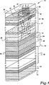
第1図は、従来技術による、プレーナ型かつ電流誘導型の、GaAs/AlGaAs頂面発光型垂直空洞レーザを示す概略図である。
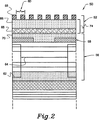
第2図は、上部ミラーが共振反射器と分布ブラッグ反射器の組合せを含む、プレーナ型かつ電流誘導型の、GaAs/AlGaAs頂面発光型垂直空洞レーザを示す概略図である。
第3図は、導電性になるように構築されたときの共振反射器の、低下した反射率を示すグラフである。
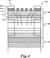
第4図は、上部接点が、導電性共振反射器の導波路回折格子の上部に位置決めされた、第2図に示すものと同様の垂直空洞レーザを示す概略図である。
第5A図は、共振反射器の導波路回折格子が上部接点として機能する、第3図に示すものと同様の垂直空洞レーザを示す概略図である。
第5B図は、共振反射器の導波路回折格子が接点と異なる材料から形成されることを以外第5A図に示すものと同様の、垂直空洞レーザを示す概略図である。
第6図は、上部ミラーを帯域幅の広い共振反射器で置き換えた、垂直空洞レーザを示す概略図である。
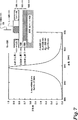
第7図は、広帯域共振反射器の反射率特性を示すグラフである。
第8A図は、上部ミラーが共振反射器と分布ブラッグ反射器を組み合わせて含む、共振空洞フォトダイオード(RCPD)を示す概略図である。
第8B図は、共振反射器214がスペーサ層216上に直接配置された、共振空洞フォトダイオード(RCPD)212を示す概略図である。
第9A図は、波長分割多重化、偏光分割多重化(polarization division multiplexing)、および空間分割多重化の助けとなる実施形態を含む、データ通信/電気通信、処理、交換などのためのいくつかの光電子デバイスを示す例示的な概略図である。
第9B図は、いくつかのVCSEL放射器およびRCPD受光器を示す例示的な概略図である。
第9C図は、VCSEL放射器、いくつかのRCPD受光器、およびそれらの間の光学的ファン・アウト素子を示す例示的な概略図である。
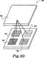
第9D図は、単一のモノリシック・デバイス上に位置するVCSEL放射器といくつかのRCPD受光器との間の通信を提供するシステムを示す例示的な概略図である。
好ましい実施形態の詳細な説明
第1図は、従来技術による、プレーナ型かつ電流誘導型の、GaAs/AlGaAs頂面発光型垂直空洞レーザ10を示す概略図である。n型にドーピングしたガリウムヒ素(GaAs)基板14にn型接点12が形成されている。基板14は第1の型(すなわちn型)の不純物でドーピングされる。n型ミラー・スタック16は基板14上に形成される。スタック16の上にはスペーサ18が形成される。スペーサ18は、活性領域22を取り囲む底部閉込め層20および上部閉込め層24を有する。p型ミラー・スタック26は、上部閉込め層24上に形成される。p型金属層28はスタック26上に形成される。放出領域はパッシベーション層30を有することがある。
分離領域29は、活性領域を通る電流の流れ27の区域を制限する。領域29は、深いH+イオン注入によって形成することができる。直径「g」は、所望の活性区域、したがってVCSEL10の利得アパーチャ(gain aperture)を提供するように設定することができる。さらに、直径「g」は、特に非導電性領域29を通る、p型ミラー・スタック26の所望の抵抗によって設定することができる。こうして、非導電性領域29は利得誘導機能を実行する。直径「g」は、通常は、注入ステップ中の横方向のばらつきなどの製作制限によって制限される。
出口アパーチャ34の直径「w」は、非導電性領域29の直径「g」より小さくすることができる。これにより、接触抵抗を低下させ、製作時の許容差を改善することができる。より高次のモードのエネルギーのほとんどはレーザ発振空洞の中央から離れたところに集中するので、これがそのレーザが所与の駆動電流で発生させるモード数を減少させる助けとなることもある。より大きな(通常は多モードの)出力パワーを得るために、直径「w」を「g」より大きくすることもできる。
スペーサ18は、ミラー・スタック16と26の間に配置されたバルクすなわち量子井戸の活性領域を含むことができる。量子井戸活性領域22は、アルミニウムガリウムヒ素(AlGaAs)障壁層およびGaAs量子井戸層が交互に重なる層を有することができる。特にGaAsが透明となる放出波長(例えば=980nm)が望ましい場合には、InGaAs量子井戸を活性領域中で使用することもできる。スタック16および26は分布ブラッグ反射器(DBR)のスタックであり、ドーピングされたAlGaAsおよびアルミニウムヒ素(AlAs)の周期層を含むことができる。スタック16のAlGaAsは基板14と同じ型(例えばn型)の不純物でドーピングされ、スタック26のAlGaAsはその他の種類(例えばp型)の不純物でドーピングされる。
金属接触層12および28は、レーザ・ダイオード10の適当な電気的バイアスを可能にするオーミック接触である。レーザ・ダイオード10が、接点28を接点12に対して正の電圧にして順方向バイアスされると、活性領域22は、スタック26を通過する光31を放出する。
第2図は、共振反射器52と分布ブラッグ反射器56を含む混成上部ミラーを備えた、プレーナ型かつ電流誘導型の、GaAs/AlGaAs頂面発光型垂直空洞レーザ50を示す概略図である。本発明の一実施形態では、誘電体導波路回折格子中の導波モード共振の異常フィルタリング特性と、従来のDBRミラーの反射特性とを組み合わせる。
図示の共振反射器52は、近赤外線VCSEL中で使用するのに適した3層導波路回折格子構造を含む。この3層スタックは、VCSEL構造の基板の放出波長付近で反射防止(AR)コーティングとして機能するように設計することも、またそれとは別に導波モードの共振反射器の導波路回折格子として機能するように設計することもできる。3つの層52は、共振波長を含む少なくとも所定範囲の波長では拡散反射がほとんどない反射防止領域を形成することができる。やはり52に示す回折格子多層導波路構造により、この構造は、少なくとも共振波長では大幅に反射性が高くなる。
別法として、この3層スタックは、VCSEL構造の基板のための高反射率コーティングとして機能するように設計することも、またそれとは別に導波モードの共振反射器の導波路回折格子として機能するように設計することもできる。この実施形態では、3つの層52は、共振波長を含む少なくとも所定範囲の波長(例えば980nm付近)で拡散反射率を提供する、高反射性ミラー領域を形成する。層66および68を含む上部ミラーの全体的な拡散反射率は、レーザ発振に必要な拡散反射率未満にすることができる。これは、例えば、上部DBRミラー56中のミラー周期(mirror period)の数を減少させることによって実施することができる。回折格子層58により、導波モードの共振反射器構造52は、少なくとも共振波長付近では大幅に反射性が高くなる。上記の両実施形態では、共振反射器領域の下のDBRミラー層の数は、従来のVCSEL構成より少なくすることができる。
共振は、回折格子58のエバネッセントな1次の回折次数の波数ベクトルを、多層導波路52の伝搬モードと整合させることによって、共振反射器52中で達成される。伝搬モードは偏光に依存するので、拡散反射率は本質的に偏光選択的である。共振波長は主に回折格子の周期60によって決定され、帯域幅は主に、回折格子58の屈折率の変調および充填率によって決定される。
通常の近赤外線VCSELは、高い反射率(>99%)を必要とする。したがって、半導体だけからなるDBRは、通常は、2〜4μmの厚さの20〜40のミラー周期を必要とする。したがって、活性スペーサ領域を取り囲む上部DBRミラーおよび底部DBRミラーを含む、VCSELを完全にするために必要な上側構造は、通常は、7〜8mを超える厚さを有する200を超える層を含む。
ミラーの厚さを薄くするために、本発明の少なくとも1つの実施形態では、混成ミラー構造を企図する。混成ミラー構造は、例えば、共振反射器52およびDBRミラー56を含む。明確に図示してはいないが、底部ミラーが共振反射器構造を含むこともできることが企図されている。誘電体共振反射器52は、共振時に反射性が高くなり、この同じ波長で、対応するDBR型ミラーより反射性を高くすることができることは既知である。したがって、この混成手法を使用することにより、所与の拡散反射率で必要となるDBRミラー周期の数を減少させることができることが企図されている。
DBRミラーを通る利得誘導領域62のイオン注入中の横方向のばらつきの影響が、しばしば活性領域の横方向の寸法64を10μmまでに制限することは既知である。これは、達成可能な最低しきい値電流、単一モード動作に直接影響を及ぼし、VCSELの速度に間接的に影響を及ぼす。共振反射器を上部ミラー中に組み込むことにより、5倍から10倍薄い構造中で、同等の、またはより優れた拡散反射率特性を達成することができる。これは、より制御し易いイオン注入をもたらし、それにより活性領域の体積を減少させることができる。活性領域が小さくなると、デバイスの動作電流および動作パワーを低下させ、平面性を改善し、それによりエレクトロニクスおよびスマート・ピクセル(smart pixel)とVCSELのモノリシックな集積性を改善し、モード制御性の高い制御可能な単一モード単一偏光の放出を実現することができる。
本発明の混成手法は、エッチングしたピラー(pillar)(平坦化および/または再成長を行う、あるいは行わない)や横方向酸化、選択的成長などを含む代替の既存の利得誘導技術と両立するものであることが分かる。VCSELミラーの全体的な厚さを薄くすることにより、共振反射器は、代替の電流誘導手法の処理可能性および性能を改善することができる。
第2図に示す実施形態では、Wang他が提案するものより広い帯域幅を有する広帯域共振反射器52は、VCSEL(またはRCPD)ミラーの一方または両方に取って代わることができる、あるいは上述の1つまたは複数のDBRミラーと組み合わせて使用することができる。上記で示したように、共振反射器の帯域幅は主に、回折格子の屈折率および充填率の変調によって決定される。したがって、本発明では、VCSELおよび/またはRCPDデバイスと組み合わせて、比較的広い帯域幅(FWHM>1nm)を有する広帯域共振反射器を提供することを企図する。
共振反射器の帯域幅は、VCSELデバイスとRCPDデバイスの間のデータ通信の信頼性を高めるのに十分に広いことが好ましい。第7図は、共振波長844.6nm、FWHM=2.3nmの共振反射器から得られる反射率特性のシミュレーション結果を示すグラフである。特にRCPDデバイス、および多モード放出を行うためのVCSELデバイスの場合には、さらに広い帯域幅が企図される。
第3図は、導波路回折格子構造の任意の1つの層中の屈折率の虚数部に対して2つの値(k=0および10-5)を想定し、またその他2つの層中ではk=0であると想定して、共振反射器の拡散反射率曲線を示すグラフである。共振反射器の構造は、図示のように3層構造である。最上層、中間層、および最下層はそれぞれ、酸化インジウムスズ(ITO)、GaAs、およびAlGaAsで形成されることが好ましい。最上層、中間層、および最下層の屈折率はそれぞれ、1.96、3.5、および3.24であり、最上層、中間層、および最下層の厚さはそれぞれ、/4、3/4、/4である。これらの層は、実効反射率が3.3となる基板上にある。この構造は、1つの横波(TE)モード共振(回折格子と平行な偏光による)で、垂直共振でなく、10-6に近い低い共振外れの拡散反射率となるようにシミュレートしたものである。
屈折率の虚数部「k」は、共振反射器の光吸収率および電気伝導率に関係する。共振反射器を通して活性領域中に電流を注入するのに必要な最低導電率にほぼ対応する、k=10-5の場合には、約5%の吸収を生じる。同じ3層が、誘電体共振反射器であることを示すk=0であれば、理論上は100パーセントの拡散反射率を生じる。
電気伝導率および高い反射率を同時に実現する共振反射器を提供するのに適した材料は容易に入手することができないことが分かっている。これに鑑みて、共振反射器およびDBRミラー・スタックを組み合わせた混成ミラー手法を企図する。
3層共振反射器は、約5周期の従来のDBRと組み合わせて設けることが好ましい(第4図参照)。単純なファブリー・ペロの拡散反射率方程式を使用した直接的な分析によれば、吸収が約5%である(k=10-5)共振反射器と組み合わせた5周期DBRミラーは、全体で約99.5%の反射率を生じ、これはVCSELミラーに十分な値を超えている。DBR層の拡散反射率が、共振反射器に達する透過した光放出の強度を約10パーセントに制限するので、これは直感的に明らかである。DBRミラーの周期が5程度であっても、DBRスタックは従来のVCSELのDBRミラーより5倍以上薄い。
導電性共振反射器を用意することにより、共振反射器を通して電流を注入することができる。これにより、VCSELデバイスまたはRCPDデバイスの接点を、共振反射器上、またはその中に、活性領域からさらに離して配置することができるようになる。これにより、多くのVCSELデバイスおよびRCPDデバイスの製作を可能に、または容易にすることができる。
第4図は、上部接点102が、導電性共振反射器106の導波路回折格子104の上部に位置決めされた、第2図に示すものと同様の垂直空洞レーザ100を示す概略図である。この実施形態では、共振反射器106を導電性にし、バイアス電流がDBRミラー108を介して接点102から活性領域110に流れることができるようにしなければならない。共振反射器は、例えば、ITOを含む透明な金属などの材料、またはAlGaAsなどのドーピングした半導体材料で共振反射器を形成することによって導電性にすることが好ましい。
上記に示したように、共振反射器構造は、通常は、回折格子および導波路を含む、適当に機能する2つのエレメントを有さなければならない。回折格子は、通常は、所望の波長に十分に近い周期を有し、0次のみが伝搬し、特に1次はエバネッセントになるようにしなければならない。適当に構築すれば、回折格子は導波路としての働きもすることができることに留意されたい。
図示の共振反射器106は、回折格子層104、ならびに2つのフィルム層112および114を含む3層構造である。上部回折格子層104はITOで形成され、中間の導波路層112はGaAsから形成され、最下層114はAlGaAsから形成されることが好ましい。層112および114は、例えば炭素をドーピングして、導電率を高くすることができる。共振反射器の各層の厚さは、/4の奇数倍であることが好ましい。例えば、最上層、中間層、および最下層の厚さはそれぞれ、/4、3/4、および/4となることが好ましい。
3層共振反射器を示したが、任意数の層を使用して共振反射器を形成することができるものと考えられる。さらに、回折格子層104は、層112および114の上部に位置決めする必要はない。その代わりに、Wang他に示されているように、回折格子層104を例えば層112と114の間に位置決めすることもできる。
導波のために、3層のうち少なくとも1つの層は、共振反射器106を取り囲む材料より高い屈折率でなければならない。図示の実施形態では、この取り囲む材料は、上部では空気、底部ではDBRミラーの層118を含む層およびその下の層である。したがって、図示の実施形態では、3つの層104、112、および114のうち少なくとも1つは、空気(n=1)およびDBRミラー108の有効屈折率より大きな屈折率でなければならない。DBRミラー108は、ドーピングしたAlGaAs層から形成することができる。
第5A図は、共振反射器134の導波路回折格子132が上部接点として機能する、第3図に示すものと同様の垂直空洞面発光型レーザ130を示す概略図である。第4図に示すように上部接触層102を設けるのではなく、この実施形態では、上部接点として導波路回折格子層132を使用することを企図する。上部導波路回折格子層132は、ITOなどの透明な金属から形成することが好ましく、回折格子は、図示のようにVCSELの出口アパーチャの上または下に形成される。中間層134および最下層136はそれぞれ、GaAsおよびAlAsから形成されることが好ましい。最上DBRミラー層138はAlGaAsから形成されることが好ましい。
第5B図は、共振反射器の導波路回折格子が接点と異なる材料から形成されることを除けば第5A図に示すものと同様の、垂直空洞レーザを示す概略図である。この実施形態では、回折格子140は例えばSiO2から形成することができ、接点部分142はAuから形成することができる。これにより、VCSELデバイスまたはRCPDデバイスの代替構成を提供することができる。
第6図は、従来の上部ミラーを広帯域共振反射器152で置き換えた、垂直空洞レーザ150を示す概略図である。共振反射器の帯域幅は、Wang他が提案したものより広い。上記に示したように、共振反射器の帯域幅は、主に、回折格子の屈折率および充填率の変調によって決定される。したがって、本発明では、VCSELデバイスまたはRCPDデバイスと組み合わせて、比較的広い帯域幅(FWHM>1nm)を有する広帯域共振反射器を提供することを企図する。
共振反射器の帯域幅は、VCSELデバイスとRCPDデバイスの間のデータ通信の信頼性を高めるのに十分に広いことが好ましい。第7図は、共振波長844.6nm、FWHM=2.3nmの共振反射器のシミュレートした拡散反射率特性を示すグラフである。これらのより広い帯域幅は、特にRCPDデバイス、および多モード放出を行うためのVCSELまたは共振空洞LEDの場合に企図される。
接点156は、共振反射器152と活性領域154の間に設けられる。したがって、この実施形態では、共振反射器152は導電性である必要はなく、またDBRミラー・スタックと組み合わせる必要もない。
ただし、上記の第2図および第4図に示すように、広帯域共振反射器152をDBRと組み合わせることもできることが分かっている。また、広帯域共振反射器152を少なくとも部分的に導電性にし、構造内での接点156の位置決めをフレキシブルにすることができることも考えられる。最後に、第8A図から第8B図に関連して後述するように、広帯域共振反射器を使用して、RCPDデバイスまたはRCLEDデバイスを形成することもできる。
第8A図は、上部ミラーが共振反射器202と分布ブラッグ反射器204を組み合わせて含む、共振空洞フォトダイオード(RCPD)200を示す概略図である。図示の実施形態では、共振反射器202は導電性となり、回折格子層210は上部接点の働きもする。この混成ミラー手法の利点は、共振反射器202を導電性にすることができ、導電性共振反射器202中の反射率の損失分をDBRミラー204によって提供することができる点である。
RCPDの応用例では、Wang他が提案したものより帯域幅が広く反射率が低い広帯域共振反射器202は、従来のRCPDのDBRミラーの一方または両方に取って代わる(第8B図参照)ことも、図示のRCPDのDBRミラーの1つまたは複数と組み合わせて使用することもできる。上記に示したように、共振反射器の帯域幅は、主に、回折格子の屈折率および充填率の変調によって決定される。したがって、本発明では、RCPDデバイス200と組み合わせて、比較的広い帯域幅(FWHM>1nm)を有する広帯域共振反射器を提供することを企図する。
共振反射器の帯域幅は、ソースとRCPDデバイスの間のデータ通信の信頼性を高めるのに十分に広いことが好ましい。第7図は、共振波長844.6nm、FWHM=2.3nmの共振反射器を示すグラフである。RCPDデバイスの波長吸収を1nmより大きくし、例えば送信側のVCSELデバイスおよび/または受信側のRCPDデバイスを製造する際の許容差、デバイスの位置合わせ(例えば入射角)、ノイズ、熱、ならびにその他の要因を含むいくつかの要因を補償すると有利であることがある。
第8B図は、共振反射器214がスペーサ層216上に直接配置された、共振空洞フォトダイオード(RCPD)212を示す概略図である。この実施形態では、従来のDBR上部ミラーは、共振反射器214で取って代わられている。共振反射器214の帯域幅は、ソースとRCPDデバイスの間のデータ通信の信頼性を高めるのに十分に広いことが好ましい。
第8A図および第8B図は、いくつかの例示的なRCPD設計の特徴を示す図であり、その一部は当技術分野で既知である。第1に、RCPDデバイスの上部または底部のどちらかから光がRCPDデバイスに入射できることは既知である。第8A図は、RCPDデバイスの上部から光が入射する場合を示す。第8B図は、RCPDデバイスの底部から光が入射する場合を示す。
図示のように光をRCPD212の底部に入射させて基板を通すために、RCPD212は約980nmで動作することができるものと企図する。870nmより長い波長を有する光は一般にGaAs基板に吸収されず、基板220をそのまま通過して底部ミラー中に入ることができることは既知である。RCPD212が980nmで動作するようにするために、活性領域218が、約850nmで動作する従来のGaAs量子井戸構造ではなく、InGaAs量子井戸構造を含むように企図する。
第9A図は、データ通信/電気通信、処理、交換などに使用することができる、いくつかのVCSELデバイス、RCLEDデバイス、および/またはRCPDデバイスを示す例示的な概略図である。集積共振反射器を有するVCSELデバイスおよびRCPDデバイスは、本質的にサイズが小さく、それに付随してパワーが低く速度が速いことにより、高密度高度並列な空間分割多重化(SDM)、波長分割多重化(WDM)、および/または偏光分割多重化(PDM)の利用分野に良く適合する。光通信、処理、交換などは、本発明のデバイスを使用するものと企図されている。
上記に示したように、共振反射器は、偏光出力を生じる導波路回折格子を含む。したがって、共振反射器とRCPDデバイスの組合せは、1つの望ましい偏光を有する光信号しか検出することができない。同様に、導波路回折格子は、所望の波長を選択することができる。通常は、回折格子のピッチおよび充填率により、所望の波長が選択される。したがって、共振反射器とRCPDデバイスの組合せは、所望の波長の光信号しか検出することができない。
詳細に第9A図を参照すると、モノリシックに形成されたいくつかのデバイスがまとめて250で示してある。導波路回折格子は、何本かの平行線として各デバイスについて示してある。第1のデバイス252は、第1の方向に延びる第1のピッチの導波路回折格子を有する。回折格子の方向によって、回折格子で共振反射された光の偏光が決定される。VCSELデバイスの場合には、こうして出力放出は本質的に偏光する。RCPDデバイスの場合には、導波路回折格子と整合する偏光を有する光だけがRCPD空洞によって共振反射される。
回折格子のピッチによって、回折格子で共振する光の波長が決定される。VCSELデバイスの場合には、出力放出は本質的に波長選択的である。RCPDデバイスの場合には、選択された波長を有する光だけがRCPD空洞中で十分に反射される。
第2のデバイス254は、やはり第1の方向に延びる第2のピッチの導波路回折格子を有するものとして示してある。したがって、第2のデバイス254は、第1のデバイス252と同じ方向に偏りを有する。ただし、第2のデバイスの導波路のピッチが狭くなるほど、第1のデバイス252より短い波長を選択する傾向がある。
第3のデバイス256は、第1の方向に延びる第3のピッチの導波路回折格子を有するものとして示してある。したがって、第3のデバイス256は、第1のデバイス252および第2のデバイス254と同じ方向に分極する。第3のデバイス256の導波路のピッチが広くなるほど、第1のデバイス252および第2のデバイス254より長い波長を選択する傾向がある。
最後に、第4のデバイス258は、第2の方向に延びる第4のピッチの導波路回折格子を有するものとして示してある。したがって、第4のデバイス258は、第1、第2、および第3のデバイスと直交する方向に分極する。第4のデバイス258の導波路のピッチが狭くなるほど、第1、第2、および第3のデバイスより短い波長を選択する傾向がある。
容易に分かるように、回折格子のピッチおよび/または方向を変えることにより、設計者はリソグラフィによって対応するデバイスの動作波長および偏光を両方とも制御することができる。これにより、分散型の波長および偏光ノードを有するSDM/WDM/PDMの混成アーキテクチャを可能にすることができる。さらに、任意の偏光を有する光を認めることが望ましい場合には、交差した2つの回折格子が互いに直交するように位置合わせされた共振反射器を製作することができる(例えば2重回折格子)。
VCSELデバイスおよびRCPDデバイスに必要な厚さを薄くすると、当然、集積化への適応性は高くなる。平面性が向上すること、および標準的な半導体プレーナのバッチ製作プロセスを利用することにより、生産性を改善することができる。共振反射器の波長、角度、および帯域幅の特性を容易に制御することができることにより、複数素子の集積回路の構築にフレキシビリティを持たせることができる。
共振回折格子の波長選択可能性は、ディスプレイの利用分野にも適用可能である。回折格子自体が動作波長を決定し、製作がリソグラフィで行われるので、横変位波長依存性放射器(laterally-displaced wavelength dependent emitter)が企図される。これは、疑似同調可能レーザ光源として働くこともできる。波長同調可能なVCSELおよび検出器は、分光および感知の利用分野で使用することもできる。
偏光を制御できることに伴う性能の改善は、偏光に敏感な光学的読取り/書込みの利用分野に向いている。CD、DVD、およびホログラフィック記憶装置の応用例には様々な形態が含まれる。レーザ・プリンタのヘッドにも有利であろう。この性能上の利点、およびより薄いミラーを使用することは、通常の完全にエピタキシャルなDBRが極めて厚くなり、多くの層の2倍の厚さを必要とすることがある可視波長までVCSELを拡大する際にさらに重要になる。
第9B図は、いくつかのVCSEL放射器およびRCPD受光器を示す例示的な概略図である。このシステムを概略的に270で示す。第1のVCSELデバイス272は、第1の偏光および第1の波長を有する光を出力する。第2のVCSELデバイス274は、第1のVCSELデバイス272と同じ方向に偏光するが、波長が異なる光を出力する。この例示的な実施形態では、第1のVCSELデバイス272および第2のVCSELデバイス274はそれぞれ、単一のモノリシック・デバイス上に設けられる。
第2のモノリシック・デバイス上には、第1のRCPDデバイス276および第2のRCPDデバイス278が位置決めされる。第1のRCPDデバイス276は、第1のVCSELデバイス272の導波路回折格子と整合する導波路回折格子を有する。したがって、第1のRCPDデバイス276は、第1のVCSELデバイス272の光出力を受けることができる。同様に、第2のRCPDデバイス278は、第2のVCSELデバイス274の導波路回折格子と整合する導波路回折格子を有する。したがって、第2のRCPDデバイス278は、第2のVCSELデバイス274の光出力を受けることができる。図示の例示的な実施形態では、第2のモノリシック・デバイスは第1のモノリシック・デバイスから横方向に離れている。
第9C図は、VCSEL放射器、いくつかのRCPD受光器、およびそれらの間の光学的ファン・アウト素子を示す例示的な概略図である。このシステムでは、VCSELデバイス302は、第1の偏光および第1の波長を有する光出力を提供する。この光出力は、図示のように光学的ファン・アウト素子304によって分割される。光学的ファン・アウト素子304は、RCPDデバイス306、308、および310に光を出力する。
RCPDデバイス306は、VCSELデバイス302と同じ向きに配向された導波路回折格子を有するが、その回折格子のピッチはVCSELデバイス302とは異なる。したがって、RCPDデバイス306は、VCSELデバイス302の光出力によって活性化されない。
RCPDデバイス310は、VCSELデバイス302と直交するように配向された導波路回折格子を有し、その回折格子のピッチもVCSELデバイス302とは異なる。したがって、RCPDデバイス310は、VCSELデバイス302の光出力によって活性化されない。
最後に、RCPDデバイス308は、VCSELデバイス302の配向およびピッチと整合する導波路回折格子を有する。したがって、RCPDデバイス308は、VCSELデバイス302の光出力によって活性化される。
第9D図は、単一のモノリシック・デバイス上に位置するVCSEL放射器といくつかのRCPD受光器との間で通信するシステムを示す例示的な概略図である。このシステムを概略的に350に示す。VCSELデバイス352は、第1の偏光および第1の波長を有する光を出力する。光出力は、図示のように光学素子354によって反射され、分配される。その後、RCPDデバイス356、358、および360は反射された光出力にさらされる。
RCPDデバイス356は、VCSELデバイス352と同じ向きに配向された導波路回折格子を有するが、その回折格子のピッチはVCSELデバイス352とは異なる。したがって、RCPDデバイス356は、VCSELデバイス352の光出力によって活性化されない。同様に、RCPDデバイス358は、VCSELデバイス352と同じ向きに配向された導波路回折格子を有するが、その回折格子のピッチはVCSELデバイス352とは異なる。したがって、RCPDデバイス358は、VCSELデバイス352の光出力によって活性化されない。
しかし、RCPDデバイス360は、VCSELデバイス352の配向およびピッチと整合する導波路回折格子を有する。したがって、RCPDデバイス360は、VCSELデバイス352の光出力によって活性化される。
これらの例示的な実施形態は、VCSEL放射器およびRCPD受光器と組み合わせて設けた導波路回折格子が、SDM、WDM、および/またはPDMの応用分野を容易にサポートすることを示している。光通信、処理、および交換などは、本発明のデバイスを使用するものと企図されている。
以上、本発明の好ましい実施形態について述べたが、本明細書に見られる教示は、添付の特許請求の範囲内でその他の実施形態に適用することができることを当業者なら容易に理解するであろう。 Background of the Invention
The present invention relates to the field of optoelectronic devices, and more particularly to photoelectric devices that use reflectors, such as vertical cavity surface emitting lasers and resonant cavity photodetectors.
Conventional semiconductor lasers are widely used in modern technology as light sources selected for various devices such as communication systems and compact disc players. In many of these applications, a semiconductor laser is coupled to a semiconductor receiver (eg, a photodiode) via an optical fiber link or free space. This configuration can provide a high-speed communication path.
A typical edge-emitting semiconductor laser has a double heterostructure in which most of both surfaces of a high refractive index layer having a small band gap are sandwiched between low refractive index layers having a large band gap. A layer with a small bandgap is called an “active layer”, and the difference in bandgap and refractive index serves to confine charge carriers and light energy in the active layer or region. Both ends of the active layer have mirror facets that form laser cavities. The cladding layer has the opposite conductivity type, and when current flows through this structure, electrons and holes combine in the active layer to generate light.
Another type of semiconductor laser that has emerged over the last decade is a surface emitting laser. Several types of surface emitting lasers have been developed. One particularly promising of these lasers is called the “Vertical Cavity Surface Emitting Laser” (VCSEL). (Examples of this laser include, for example, “Surface-emitting microlasers for photonic switching and interactive connections”,Optical Engineering29, 210-214, March 1990. As another example, Yong H., issued May 19, 1992, which is hereby incorporated by reference. US Pat. No. 5,115,442 entitled “Top-emitting Surface Emitting Laser Structures” by Lee et al., And Mary K., issued December 12, 1995, which is hereby incorporated by reference. Note U.S. Pat. No. 5,475,701, entitled “Integrated Laser Power Monitor” by Hibbs-Brenner. Also, “Top-surface-emitting GaAs four-quantum-well lasers emitting at 0.85 μm”,Electronics Letters26, 710-711, May 24, 1990. )
Vertical cavity surface emitting lasers offer many performance and potential productivity advantages over conventional edge emitting lasers. Many benefits associated with these geometries, such as adaptability to one- and two-dimensional arrays, wafer-level quality, and desirable beam characteristics (typically circularly symmetric, low-divergence beams) Is included.
A VCSEL typically has an active region with a bulk or one or more quantum well layers. There are mirror stacks on either side of the active region, which usually have the property that each layer is typically a quarter wavelength thick at the wavelength of interest (in the medium), thereby making the mirror a laser cavity. Formed by alternately arranged semiconductor layers. There are regions of opposite conductivity type on either side of the active region, and the laser is typically turned on and off by changing the current through the active region.
High yield and high performance VCSELs have been demonstrated and commercialized. AlGaAs-based top-surface-emitting VCSELs can be manufactured in a manner similar to semiconductor integrated circuits and can be adapted for low-cost mass production and integration with existing electronic technology platforms. it can. In addition, the homogeneity and reproducibility of VCSELs also uses standard, unmodified commercial metalorganic vapor phase epitaxy (MOVPE) chambers and molecular beam epitaxy (MBE) which gives extremely high device yields. Has been proven.
VCSELs have performance aspects in high-speed (eg Gbit / s) and medium-range (eg about 1000 meters or less) single-channel or multi-channel data link applications and in many optical and / or image processing applications. And is expected to provide cost benefits. This is brought about by their inherent geometry that provides a potentially low cost, high performance transmitter with desirable desirable features.
Most practical size VCSELs are inherently multi-mode. The lowest order single mode VCSEL is preferred for coupling into a single mode optical fiber, and is advantageous in free space and / or wavelength sensitive systems, with standard 50 μm and 62.5 μm GRIN multimode fibers It may be beneficial to use when increasing the bandwidth-length product of. However, while the short optical cavity (2) of the VCSEL is advantageous for single longitudinal mode emission, it has long been known that multi-wavelength (10) lateral dimensions facilitate multiple transverse mode operation.
The higher order modes usually have a higher energy lateral concentration away from the center of the lasing cavity. Thus, the most obvious way to cause lasing in the lowest order circularly symmetric mode is to make the lateral dimensions of the active region small enough to prevent higher order modes from reaching the threshold That is. However, this requires that the lateral dimension be less than about 5 m in the case of a normal VCSEL. Such small areas can lead to excessive resistance and push the limits available with conventional fabrication techniques. This is especially true when the implantation depth exceeds about 1 m, where lateral variation can be a limiting factor. Thus, lateral mode control remains difficult with practically sized VCSELs.
One proposed approach to help control transverse modes in VCSELs is to use a dimension “W” for the exit window that is smaller than the excitation dimension “g” of the lasing cavity. This technique is described in Morgan et al., “Transverse Mode Control of Vertical-City Top-Surface-Emitting Lasers”, IEEE Photo. Tech. Lett. Vol. 4, no. 4, 374 pages (April 1993). Morgan et al. Make the lateral dimension “w” of the exit window in the top metal contact smaller than the gain guide aperture “g” (which determines the lateral dimension of the excitation area of the lasing cavity). Propose that. In this configuration, the upper metal contact (usually gold) interfaces directly with the top layer of the upper semiconductor mirror stack around the excitation area of the lasing cavity.
In the exit window, the top layer of the upper semiconductor mirror stack is directly interfaced with air or the like. Morgan et al. Described that this configuration is a transverse mode because the reflectivity of the gold-semiconductor interface may be out of phase and / or non-specular, and thus may be less reflective than the semiconductor-air interface. Suggests that it can help control the release.
Lower reflectivity at the gold-semiconductor interface may reduce the possibility of higher order modes occurring in and around the lasing cavity. This effectively reduces the lateral optical dimension of the excitation of the lasing cavity and allows for larger fabrication dimensions.
The limitation of this approach is to effectively control the difference between the reflectivity at the gold-semiconductor reflectivity interface and the reflectivity at the semiconductor-air interface, especially at higher bias currents. However, it cannot be made large enough. Furthermore, the diffuse reflectance at the gold-semiconductor interface and at the semiconductor-air interface is not well controlled or reproducible for commercial applications. Furthermore, the efficiency of these “spatial filtered” VCSELs is not optimal.
Apart from mode control, another limitation of many prior art VCSEL devices is mode stability. The emission modes emitted by conventional VCSEL devices often depend on temperature effects such as thermal lenses, spatial hole burning, and bias conditions. Thus, conventional VCSEL devices cannot provide a stable output emission mode under all expected operating conditions.
S. S. Wang and R.W. "Theory and Applications of Guided-mode Resonance Filters" by Magnusson, Applied Optics, Vol. 32, no. 14, May 10, 1993, discusses dielectric resonant reflection filters. Wang et al. Proposes to use a dielectric antireflective coating with a dielectric diffraction grating having a high spatial frequency. It is stated that a 100% reflective narrow band spectrally selective mirror can be realized using this approach.
The design of a narrowband resonant reflection filter based on a multilayer waveguide grating structure is described in S.A. S. Wang and R.W. “Multilayer Waveguide-Grating Filters” by Magnusson, Applied Optics, Vol. 34, no. 14, May 10, 1995. Examples of single-layer, double-layer, and triple-layer waveguide grating filters are given. Here, Wang et al. Specifically proposes to use their narrowband dielectric reflective filters as mirrors in VCSEL arrays.
There are some limitations to using narrowband dielectric resonant reflection filters as mirrors in VCSEL arrays, some of which are described below. First, it should be noted that Wang et al.'S dielectric reflective filters are not conductive and therefore cannot be used in current injection paths, for example, paths through the corresponding active region from the contacts of the VCSEL device. The mirror of a conventional VCSEL device is usually a semiconductor distributed Bragg reflector (DBR). The semiconductor DBR mirror can be conductive and often provides a current path from the contact point of the VCSEL to the active region. For example, when using Wang et al.'S dielectric resonant reflection filter instead of the top mirror of a VCSEL device, the upper contact must be positioned between the dielectric reflection filter and the active region. This can severely limit the design of many VCSEL structures.
Second, the proposed “narrowband” dielectric resonant reflection filter of Wang et al. Cannot have a sufficiently large operating wavelength in many optoelectronic applications, including those in optical communications. S. S. Wang and R.W. “Multilayer Waveguide-Grating Filters” by Magnusson, Applied Optics, Vol. 34, no. 14, May 10, 1995, Wang et al. Provide examples of single-layer, double-layer, and triple-layer waveguide grating filters. In each case, the full width at half maximum (FWHM) diffuse reflectance bandwidth is less than about 1 nm. Resonances below 1 nm cannot provide a sufficiently large bandwidth for use in a resonant cavity photodetector (RCPD) or other photodetector.
Resonant cavity photodetectors are typically constructed similar to VCSELs, but operate in the reverse bias mode. Resonant cavity photodetectors can be more efficient than standard photodiodes because light that is incident on the cavity through one of the mirrors can be efficiently reflected many times through the active region. it can. In this way, light can be reflected between mirror stacks until it is absorbed into the active region or leaks through one of the mirror stacks. Since the mirror stack is usually highly reflective near resonance, most of the light incident on the cavity is absorbed in the active region.
The Wang et al. “Narrowband” dielectric resonant reflection filter seeks to achieve a very narrow bandwidth and possibly increase the frequency selectivity of the filter. However, in many VCSEL applications such as VCSEL / RCPD electro-optic communication paths, it may be advantageous to increase the wavelength bandwidth of the RCPD device, manufacturing tolerances of the VCSEL and RCPD devices, device alignment, It must be wide enough to compensate for several factors including noise, heat, and other factors. This should also be advantageous when constructing multimode VCSELs using resonant reflectors. This allows higher bandwidth detectors to be used in communication links that exhibit finite wavelength variations and high bandwidth sources.
Summary of the Invention
The present invention overcomes many of the disadvantages of the prior art by providing optoelectronic devices with integrated resonant reflectors, such as VCSEL devices and RCPD devices. The integrated resonant reflector can be conductive so that a bias current flows through it. Thereby, the design of the VCSEL device and the RCPD device can be made more flexible. Making the resonant reflector more conductive reduces the overall reflectivity that the resonant reflector can achieve, so a resonant reflector is provided in combination with a distributed Bragg reflector (DBR) mirror and is required for VCSEL or RCPD design. It is also possible to achieve a high overall diffuse reflectance.
A wide bandwidth resonant reflector (FWHM> 1 nm) can be used to produce a VCSEL or RCPD with a wider bandwidth. The bandwidth can be wide enough to increase the reliability of data communication between such devices. Further, in VCSEL applications where multimode emission is desirable, a wider bandwidth resonant reflector can be used.
[Brief description of the drawings]
Other objects of the present invention and many of the attendant advantages of the present invention will become readily apparent as the invention is better understood by reference to the following detailed description and considered in conjunction with the accompanying drawings. You will understand. Like reference numerals refer to like parts throughout the drawings.
FIG. 1 is a schematic diagram showing a planar and current-induced GaAs / AlGaAs top emitting vertical cavity laser according to the prior art.
FIG. 2 is a schematic diagram showing a planar and current-guided GaAs / AlGaAs top-emitting vertical cavity laser in which the upper mirror includes a combination of resonant and distributed Bragg reflectors.
FIG. 3 is a graph showing the reduced reflectivity of a resonant reflector when constructed to be conductive.
FIG. 4 is a schematic diagram showing a vertical cavity laser similar to that shown in FIG. 2 with the top contact positioned on top of the waveguide grating of the conductive resonant reflector.
FIG. 5A is a schematic diagram showing a vertical cavity laser similar to that shown in FIG. 3, in which the waveguide grating of the resonant reflector functions as an upper contact.
FIG. 5B is a schematic diagram showing a vertical cavity laser similar to that shown in FIG. 5A except that the waveguide grating of the resonant reflector is formed from a different material than the contacts.
FIG. 6 is a schematic diagram showing a vertical cavity laser with the upper mirror replaced by a wide bandwidth resonant reflector.
FIG. 7 is a graph showing the reflectance characteristics of the broadband resonant reflector.
FIG. 8A is a schematic diagram showing a resonant cavity photodiode (RCPD) in which the upper mirror includes a combination of a resonant reflector and a distributed Bragg reflector.
FIG. 8B is a schematic diagram showing a resonant cavity photodiode (RCPD) 212 with a
FIG. 9A illustrates several for data communication / telecommunications, processing, exchange, etc., including embodiments that aid in wavelength division multiplexing, polarization division multiplexing, and space division multiplexing. 1 is an exemplary schematic diagram illustrating an optoelectronic device. FIG.
FIG. 9B is an exemplary schematic diagram illustrating several VCSEL emitters and RCPD receivers.
FIG. 9C is an exemplary schematic diagram illustrating a VCSEL radiator, several RCPD receivers, and an optical fan-out element therebetween.
FIG. 9D is an exemplary schematic diagram illustrating a system for providing communication between a VCSEL emitter and several RCPD receivers located on a single monolithic device.
Detailed Description of the Preferred Embodiment
FIG. 1 is a schematic diagram illustrating a planar and current-induced GaAs / AlGaAs top emitting
The diameter “w” of the
The
Metal contact layers 12 and 28 are ohmic contacts that allow proper electrical biasing of
FIG. 2 is a schematic diagram showing a planar, current-induced, GaAs / AlGaAs top emitting
The illustrated
Alternatively, the three-layer stack can be designed to function as a high reflectivity coating for a VCSEL structure substrate, or alternatively, function as a waveguide grating for a guided mode resonant reflector. It can also be designed as follows. In this embodiment, the three
Resonance is achieved in the
Ordinary near-infrared VCSELs require high reflectivity (> 99%). Therefore, a DBR consisting only of a semiconductor typically requires 20 to 40 mirror periods with a thickness of 2 to 4 μm. Thus, the upper structure required to complete the VCSEL, including the top and bottom DBR mirrors surrounding the active spacer region, typically includes over 200 layers having a thickness of over 7-8 m.
In order to reduce the mirror thickness, at least one embodiment of the present invention contemplates a hybrid mirror structure. The hybrid mirror structure includes, for example, a
It is known that the effects of lateral variations during ion implantation of the
The hybrid approach of the present invention is compatible with alternative existing gain induction techniques including etched pillars (with or without planarization and / or regrowth), lateral oxidation, selective growth, etc. It turns out that it is. By reducing the overall thickness of the VCSEL mirror, the resonant reflector can improve the processability and performance of alternative current induction techniques.
In the embodiment shown in FIG. 2, a broadband
The bandwidth of the resonant reflector is preferably wide enough to increase the reliability of data communication between the VCSEL device and the RCPD device. FIG. 7 is a graph showing a simulation result of reflectance characteristics obtained from a resonant reflector having a resonant wavelength of 844.6 nm and FWHM = 2.3 nm. Even wider bandwidths are contemplated, particularly in the case of RCPD devices and VCSEL devices for multimode emission.
FIG. 3 shows two values (k = 0 and 10) for the imaginary part of the refractive index in any one layer of the waveguide grating structure.-Five), And assuming that k = 0 in the other two layers, it is a graph showing the diffuse reflectance curve of the resonant reflector. The structure of the resonant reflector is a three-layer structure as shown. The uppermost layer, the intermediate layer, and the lowermost layer are preferably formed of indium tin oxide (ITO), GaAs, and AlGaAs, respectively. The refractive indices of the top layer, the middle layer, and the bottom layer are 1.96, 3.5, and 3.24, respectively, and the thicknesses of the top layer, the middle layer, and the bottom layer are respectively / 4, 3 / 4, / 4. These layers are on a substrate with an effective reflectivity of 3.3. This structure is a single transverse wave (TE) mode resonance (due to polarization parallel to the diffraction grating) and not a vertical resonance.-6It was simulated so as to have a diffuse reflectance with a low off-resonance value close to.
The imaginary part “k” of the refractive index is related to the light absorptance and electrical conductivity of the resonant reflector. Approximately corresponding to the lowest conductivity required to inject current into the active region through the resonant reflector, k = 10-FiveIn this case, an absorption of about 5% occurs. If k = 0, which indicates that the same three layers are dielectric resonant reflectors, it would theoretically produce 100 percent diffuse reflectance.
It has been found that materials suitable for providing a resonant reflector that simultaneously achieves electrical conductivity and high reflectivity are not readily available. In view of this, a hybrid mirror approach that combines a resonant reflector and a DBR mirror stack is contemplated.
The three-layer resonant reflector is preferably provided in combination with a conventional DBR having about 5 cycles (see FIG. 4). According to a direct analysis using the simple Fabry-Perot diffuse reflectance equation, the absorption is about 5% (k = 10-Five) A five-period DBR mirror combined with a resonant reflector yields a total reflectivity of about 99.5%, which is more than sufficient for a VCSEL mirror. This is intuitively obvious because the diffuse reflectance of the DBR layer limits the intensity of transmitted light emission reaching the resonant reflector to about 10 percent. Even if the period of the DBR mirror is about 5, the DBR stack is more than 5 times thinner than the DBR mirror of the conventional VCSEL.
By providing a conductive resonant reflector, current can be injected through the resonant reflector. This allows the contact of the VCSEL device or RCPD device to be placed on or in the resonant reflector further away from the active region. This can allow or facilitate the fabrication of many VCSEL and RCPD devices.
FIG. 4 is a schematic diagram showing a
As indicated above, a resonant reflector structure typically must have two elements that function properly, including a diffraction grating and a waveguide. The diffraction grating usually has a period sufficiently close to the desired wavelength, so that only the 0th order propagates, in particular the 1st order must be evanescent. Note that if constructed properly, the diffraction grating can also serve as a waveguide.
The illustrated
Although a three-layer resonant reflector is shown, it is believed that any number of layers can be used to form a resonant reflector. Furthermore, the
For waveguiding, at least one of the three layers must have a higher refractive index than the material surrounding the
FIG. 5A is a schematic diagram showing a vertical cavity
FIG. 5B is a schematic diagram showing a vertical cavity laser similar to that shown in FIG. 5A except that the waveguide grating of the resonant reflector is formed from a different material than the contacts. In this embodiment, the
FIG. 6 is a schematic diagram showing a
The bandwidth of the resonant reflector is preferably wide enough to increase the reliability of data communication between the VCSEL device and the RCPD device. FIG. 7 is a graph showing simulated diffuse reflectance characteristics of a resonant reflector having a resonant wavelength of 844.6 nm and FWHM = 2.3 nm. These wider bandwidths are contemplated especially for RCPD devices and VCSELs or resonant cavity LEDs for multimode emission.
A
However, it has been found that the broadband
FIG. 8A is a schematic diagram illustrating a resonant cavity photodiode (RCPD) 200 in which the upper mirror includes a combination of a
In RCPD applications, the broadband
The bandwidth of the resonant reflector is preferably wide enough to increase the reliability of data communication between the source and the RCPD device. FIG. 7 is a graph showing a resonant reflector having a resonant wavelength of 844.6 nm and FWHM = 2.3 nm. The wavelength absorption of the RCPD device is greater than 1 nm, for example, tolerance in manufacturing the transmitting VCSEL device and / or the receiving RCPD device, device alignment (eg incident angle), noise, heat, and other It may be advantageous to compensate for several factors, including factors.
FIG. 8B is a schematic diagram showing a resonant cavity photodiode (RCPD) 212 with a
FIGS. 8A and 8B illustrate some exemplary RCPD design features, some of which are known in the art. First, it is known that light can enter the RCPD device from either the top or bottom of the RCPD device. FIG. 8A shows the case where light enters from the top of the RCPD device. FIG. 8B shows the case where light enters from the bottom of the RCPD device.
It is contemplated that
FIG. 9A is an exemplary schematic diagram illustrating several VCSEL devices, RCLED devices, and / or RCPD devices that can be used for data / telecommunications, processing, switching, and the like. VCSEL and RCPD devices with integrated resonant reflectors are inherently small in size, with concomitant low power and high speed, resulting in high density highly parallel space division multiplexing (SDM), wavelength division multiplexing (WDM) and / or well suited to the field of application of polarization division multiplexing (PDM). Optical communications, processing, switching, etc. are contemplated using the device of the present invention.
As indicated above, the resonant reflector includes a waveguide grating that produces a polarized output. Thus, the combination of the resonant reflector and the RCPD device can only detect an optical signal having one desired polarization. Similarly, the waveguide diffraction grating can select a desired wavelength. Usually, a desired wavelength is selected depending on the pitch and filling factor of the diffraction grating. Therefore, the combination of the resonant reflector and the RCPD device can detect only an optical signal having a desired wavelength.
Referring in detail to FIG. 9A, several devices that are monolithically formed are shown collectively at 250. The waveguide grating is shown for each device as several parallel lines. The
The wavelength of light resonating in the diffraction grating is determined by the pitch of the diffraction grating. In the case of a VCSEL device, the output emission is essentially wavelength selective. In the case of an RCPD device, only light having a selected wavelength is fully reflected in the RCPD cavity.
The
The
Finally, the
As can be readily seen, by changing the pitch and / or orientation of the diffraction grating, the designer can control both the operating wavelength and polarization of the corresponding device by lithography. This can enable a hybrid SDM / WDM / PDM architecture with dispersive wavelength and polarization nodes. Further, if it is desired to recognize light having an arbitrary polarization, a resonant reflector can be fabricated in which two crossed diffraction gratings are aligned so as to be orthogonal to each other (eg, a double diffraction grating). .
When the thickness required for the VCSEL device and the RCPD device is reduced, the adaptability to integration is naturally increased. Productivity can be improved by improving planarity and utilizing a standard semiconductor planar batch fabrication process. The ability to easily control the wavelength, angle, and bandwidth characteristics of the resonant reflector allows flexibility in the construction of a multi-element integrated circuit.
The wavelength selectability of the resonant diffraction grating is also applicable to the field of display applications. A laterally-displaced wavelength dependent emitter is contemplated since the diffraction grating itself determines the operating wavelength and fabrication is done lithographically. This can also serve as a quasi-tunable laser source. Wavelength tunable VCSELs and detectors can also be used in spectroscopy and sensing applications.
The performance improvement associated with the ability to control polarization is suitable for optical read / write applications that are sensitive to polarization. Applications for CD, DVD, and holographic storage devices include various forms. It would also be advantageous for laser printer heads. This performance advantage, and the use of thinner mirrors, extends the VCSEL to visible wavelengths where the normal fully epitaxial DBR can be very thick and may require twice the thickness of many layers It becomes even more important when you do.
FIG. 9B is an exemplary schematic diagram illustrating several VCSEL emitters and RCPD receivers. This system is shown generally at 270. The
A first
FIG. 9C is an exemplary schematic diagram illustrating a VCSEL radiator, several RCPD receivers, and an optical fan-out element therebetween. In this system, the
The
The
Finally, the
FIG. 9D is an exemplary schematic diagram illustrating a system for communicating between a VCSEL emitter located on a single monolithic device and several RCPD receivers. This system is shown generally at 350. The
The
However,
These exemplary embodiments show that waveguide gratings provided in combination with VCSEL radiators and RCPD receivers easily support SDM, WDM, and / or PDM applications. Optical communications, processing, switching, etc. are contemplated using the device of the present invention.
Having described preferred embodiments of the present invention, those skilled in the art will readily appreciate that the teachings found herein may be applied to other embodiments within the scope of the appended claims. Let's go.
Claims (33)
回折格子領域を有する導波路回折格子層を含む共振反射器であって、前記上部ミラー・スタックと前記底部ミラー・スタックの少なくとも一方と隣接して位置決めされた共振反射器を含み、前記共振反射器は更に、複数の共振反射器層を含み、各共振反射器層は屈折率を有しており、少なくとも1つの屈折率の変調に依存した拡散反射率帯域幅を前記共振反射器が有しているモノリシック光電子デバイス。A monolithic optoelectronic device having a top mirror stack and a bottom mirror stack,
A resonator reflector comprising waveguide grating layer having a diffraction grating region, seen including at least one with the adjacent resonator reflector is positioned between the upper mirror stack the bottom mirror stack, said resonant reflector The resonator further includes a plurality of resonant reflector layers, each resonant reflector layer having a refractive index, the resonant reflector having a diffuse reflectance bandwidth dependent upon modulation of at least one refractive index. Monolithic optoelectronic devices.
導波路領域を含む請求項1に記載の光電子デバイス。The resonant reflector is
The optoelectronic device of claim 1 comprising a waveguide region.
第2のミラー・スタックと、A second mirror stack;
前記第1のミラー・スタックと前記第2のミラー・スタックの間に位置決めされた活性領域と、An active region positioned between the first mirror stack and the second mirror stack;
前記第1のミラー・スタックに隣接して位置決めされた共振反射器手段であって、回折格子領域を有する導電性の導波路回折格子層を含む複数層を有する共振反射器手段であって、共振波長を含む所定範囲の波長で拡散反射率をもたらす共振反射器手段とを含み、前記共振反射器手段の前記複数層に含まれる各層が屈折率を有しており、少なくとも1つの屈折率の変調に依存した拡散反射率帯域幅を前記共振反射器手段が有している光電子デバイス。Resonant reflector means positioned adjacent to the first mirror stack, the resonator reflector means having a plurality of layers including a conductive waveguide grating layer having a diffraction grating region, Resonant reflector means for providing diffuse reflectance at a predetermined range of wavelengths including wavelengths, each layer included in the plurality of layers of the resonant reflector means having a refractive index, and modulation of at least one refractive index An optoelectronic device in which the resonant reflector means has a diffuse reflectance bandwidth depending on the.
前記第2のミラー・スタックの少なくとも一部分を介して前記活性領域に電気的に結合された第2の接点手段とSecond contact means electrically coupled to the active region via at least a portion of the second mirror stack;
をさらに含む請求項12に記載の光電子デバイス。The optoelectronic device of claim 12 further comprising:
前記共振反射器領域に隣接して位置決めされた分布ブラッグ反射器(DBR)と、A distributed Bragg reflector (DBR) positioned adjacent to the resonant reflector region;
を含む混成構造第1のミラー・スタックと、A hybrid structure first mirror stack comprising:
第2のミラー・スタックと、A second mirror stack;
前記混成構造第1のミラー・スタックと前記第2のミラー・スタックとの間に位置決めされた活性領域と、An active region positioned between the hybrid structure first mirror stack and the second mirror stack;
を含む光電子デバイス。Including optoelectronic devices.
前記第2のミラー・スタックの少なくとも一部分を介して前記活性領域に電気的に結合された第2の接点手段とSecond contact means electrically coupled to the active region via at least a portion of the second mirror stack;
をさらに含む請求項22に記載の光電子デバイス。The optoelectronic device of claim 22 further comprising:
第1のミラー・スタックを基板上に形成するステップと、Forming a first mirror stack on a substrate;
活性領域を前記第1のミラー・スタック上に形成するステップと、Forming an active region on the first mirror stack;
第2のミラー・スタックを前記活性領域上に形成するステップと、Forming a second mirror stack on the active region;
複数の未充填溝を含む回折格子領域を有する導波路回折格子層を含む複数層共振反射器であって、前記複数層共振反射器に含まれる各層が屈折率を有しており、少なくとも1つの屈折率の変調に依存した拡散反射率帯域幅を前記複数層共振反射器が有し、共振波長を含む所定範囲の波長で拡散反射率をもたらす前記複数層共振反射器を前記第2のミラー・スタック上に隣接して形成するステップと、A multi-layer resonant reflector including a waveguide diffraction grating layer having a diffraction grating region including a plurality of unfilled grooves, each layer included in the multi-layer resonant reflector has a refractive index, and at least one The multi-layer resonant reflector has a diffuse reflectance bandwidth that depends on the modulation of the refractive index, and the multi-layer resonant reflector provides the diffuse reflectance at a predetermined range of wavelengths including the resonant wavelength. Forming adjacent to the stack;
前記共振反射器の少なくとも一部をドーピングして導電性にするステップとDoping at least a portion of the resonant reflector to make it conductive;
を含む方法。Including methods.
回折格子領域を有する導波路回折格子層を含む複数層を含む一体化された共振反射器を有する第1のRCPDデバイスであって、当該共振反射器の各層は屈折率を有しており、少なくとも1つの屈折率の変調に依存した拡散反射率帯域幅を当該共振反射器が有しており、当該第1のRCPDデバイスの前記共振反射器が前記VCSELデバイスのものと同じ配向を有し、前記VCSELデバイスの偏光出力を検出するようになっている第1のRCPDデバイスとA first RCPD device having an integrated resonant reflector comprising a plurality of layers including a waveguide grating layer having a diffraction grating region, wherein each layer of the resonant reflector has a refractive index, at least The resonant reflector has a diffuse reflectance bandwidth dependent on one refractive index modulation, the resonant reflector of the first RCPD device has the same orientation as that of the VCSEL device, and A first RCPD device adapted to detect the polarization output of the VCSEL device;
を含む光データ経路。Including optical data path.
一体化された共振反射器を有する第1のRCPDデバイスであって、その前記共振反射器が前記VCSELデバイスの前記導波路回折格子層に対応する、回折格子領域を有する導波路回折格子層を含む複数層を有し、当該複数層の各層は屈折率を有しており、少なくとも1つの屈折率の変調に依存した拡散反射率帯域幅を当該第1のRCPDデバイスの共振反射器が有しており、前記VCSELデバイスからの所定範囲の波長の光を検出するようになっている第1のRCPDデバイスとA first RCPD device having an integrated resonant reflector, the resonant reflector including a waveguide grating layer having a grating region corresponding to the waveguide grating layer of the VCSEL device The first RCPD device resonant reflector has a plurality of layers, each layer of the plurality of layers has a refractive index, and has a diffuse reflectance bandwidth dependent on modulation of at least one refractive index. A first RCPD device adapted to detect light in a predetermined range of wavelengths from the VCSEL device;
を含む光通信システム。An optical communication system including:
Applications Claiming Priority (3)
| Application Number | Priority Date | Filing Date | Title |
|---|---|---|---|
| US08/872,534 | 1997-06-11 | ||
| US08/872,534 US6055262A (en) | 1997-06-11 | 1997-06-11 | Resonant reflector for improved optoelectronic device performance and enhanced applicability |
| PCT/US1998/011920 WO1998057402A1 (en) | 1997-06-11 | 1998-06-10 | Resonant reflector for improved optoelectronic device performance and enhanced applicability |
Publications (2)
| Publication Number | Publication Date |
|---|---|
| JP2002506567A JP2002506567A (en) | 2002-02-26 |
| JP4237828B2 true JP4237828B2 (en) | 2009-03-11 |
Family
ID=25359775
Family Applications (1)
| Application Number | Title | Priority Date | Filing Date |
|---|---|---|---|
| JP50309399A Expired - Fee Related JP4237828B2 (en) | 1997-06-11 | 1998-06-10 | Resonant reflector with improved optoelectronic device performance and increased availability |
Country Status (6)
| Country | Link |
|---|---|
| US (1) | US6055262A (en) |
| EP (2) | EP1309051B1 (en) |
| JP (1) | JP4237828B2 (en) |
| CA (1) | CA2286838A1 (en) |
| DE (2) | DE69838761T2 (en) |
| WO (1) | WO1998057402A1 (en) |
Families Citing this family (108)
| Publication number | Priority date | Publication date | Assignee | Title |
|---|---|---|---|---|
| JP3713956B2 (en) * | 1998-05-29 | 2005-11-09 | 富士ゼロックス株式会社 | Manufacturing method of surface emitting semiconductor laser device |
| US6542527B1 (en) | 1998-08-27 | 2003-04-01 | Regents Of The University Of Minnesota | Vertical cavity surface emitting laser |
| US6291839B1 (en) | 1998-09-11 | 2001-09-18 | Lulileds Lighting, U.S. Llc | Light emitting device having a finely-patterned reflective contact |
| US6195485B1 (en) * | 1998-10-26 | 2001-02-27 | The Regents Of The University Of California | Direct-coupled multimode WDM optical data links with monolithically-integrated multiple-channel VCSEL and photodetector |
| US6816528B1 (en) * | 1998-12-30 | 2004-11-09 | Xerox Corporation | Method and structure for nitride based laser diode arrays on a conducting substrate |
| GB9916145D0 (en) * | 1999-07-10 | 1999-09-08 | Secr Defence | Control of polarisation of vertical cavity surface emitting lasers |
| JP3586594B2 (en) * | 1999-08-25 | 2004-11-10 | シャープ株式会社 | Semiconductor light emitting device and method of manufacturing the same |
| WO2001028001A1 (en) * | 1999-10-13 | 2001-04-19 | Lockheed Martin Corporation | Optical interconnect using multifunctional optical elements |
| US8111401B2 (en) * | 1999-11-05 | 2012-02-07 | Robert Magnusson | Guided-mode resonance sensors employing angular, spectral, modal, and polarization diversity for high-precision sensing in compact formats |
| US7167615B1 (en) * | 1999-11-05 | 2007-01-23 | Board Of Regents, The University Of Texas System | Resonant waveguide-grating filters and sensors and methods for making and using same |
| JP2001298212A (en) * | 2000-02-07 | 2001-10-26 | Sharp Corp | Semiconductor light emitting device and method of manufacturing the same |
| US6611544B1 (en) | 2000-04-11 | 2003-08-26 | E20 Communications, Inc. | Method and apparatus for narrow bandwidth distributed bragg reflector semiconductor lasers |
| KR100708081B1 (en) * | 2000-05-18 | 2007-04-16 | 삼성전자주식회사 | Apparatus and method for manufacturing aperture of surface light laser by selective oxidation method |
| US6829286B1 (en) * | 2000-05-26 | 2004-12-07 | Opticomp Corporation | Resonant cavity enhanced VCSEL/waveguide grating coupler |
| US6515305B2 (en) * | 2000-09-18 | 2003-02-04 | Regents Of The University Of Minnesota | Vertical cavity surface emitting laser with single mode confinement |
| US6905900B1 (en) | 2000-11-28 | 2005-06-14 | Finisar Corporation | Versatile method and system for single mode VCSELs |
| US6990135B2 (en) * | 2002-10-28 | 2006-01-24 | Finisar Corporation | Distributed bragg reflector for optoelectronic device |
| US7065124B2 (en) * | 2000-11-28 | 2006-06-20 | Finlsar Corporation | Electron affinity engineered VCSELs |
| US6727520B2 (en) * | 2000-12-29 | 2004-04-27 | Honeywell International Inc. | Spatially modulated reflector for an optoelectronic device |
| TWI227799B (en) * | 2000-12-29 | 2005-02-11 | Honeywell Int Inc | Resonant reflector for increased wavelength and polarization control |
| US6782027B2 (en) | 2000-12-29 | 2004-08-24 | Finisar Corporation | Resonant reflector for use with optoelectronic devices |
| US6836501B2 (en) * | 2000-12-29 | 2004-12-28 | Finisar Corporation | Resonant reflector for increased wavelength and polarization control |
| DE60104513T2 (en) * | 2001-01-17 | 2005-08-04 | Avalon Photonics Ltd. | A polarization stable vertical cavity surface emitting laser and method for stabilizing the polarization of such a laser |
| TW529211B (en) * | 2001-03-07 | 2003-04-21 | Ying-Jay Yang | Device structure and method for fabricating semiconductor lasers |
| US6661952B2 (en) * | 2001-05-04 | 2003-12-09 | Ut Battelle, Llc | Sub-wavelength efficient polarization filter (SWEP filter) |
| US6553053B2 (en) * | 2001-07-25 | 2003-04-22 | Luxnet Corporation | Vertical cavity surface emitting laser having improved light output function |
| GB2379797A (en) * | 2001-09-15 | 2003-03-19 | Zarlink Semiconductor Ab | Surface Emitting Laser |
| US6606199B2 (en) | 2001-10-10 | 2003-08-12 | Honeywell International Inc. | Graded thickness optical element and method of manufacture therefor |
| GB2383679A (en) * | 2001-12-27 | 2003-07-02 | Bookham Technology Plc | PIN photodiode with intrinsic region implanted with deep band gap levels |
| US6862301B2 (en) * | 2001-12-31 | 2005-03-01 | Finisar Corporation | Tunable laser assembly |
| US6717974B2 (en) * | 2002-04-01 | 2004-04-06 | Lumei Optoelectronics Corporation | Apparatus and method for improving electrical conduction structure of a vertical cavity surface emitting laser |
| KR100475858B1 (en) * | 2002-04-01 | 2005-03-18 | 주식회사 테라스테이트 | A Vertical Cavity Surface Emitting Lasers |
| US6965626B2 (en) * | 2002-09-03 | 2005-11-15 | Finisar Corporation | Single mode VCSEL |
| US6813293B2 (en) * | 2002-11-21 | 2004-11-02 | Finisar Corporation | Long wavelength VCSEL with tunnel junction, and implant |
| US6727530B1 (en) * | 2003-03-04 | 2004-04-27 | Xindium Technologies, Inc. | Integrated photodetector and heterojunction bipolar transistors |
| US20040222363A1 (en) * | 2003-05-07 | 2004-11-11 | Honeywell International Inc. | Connectorized optical component misalignment detection system |
| US20040247250A1 (en) * | 2003-06-03 | 2004-12-09 | Honeywell International Inc. | Integrated sleeve pluggable package |
| US7298942B2 (en) | 2003-06-06 | 2007-11-20 | Finisar Corporation | Pluggable optical optic system having a lens fiber stop |
| US7433381B2 (en) | 2003-06-25 | 2008-10-07 | Finisar Corporation | InP based long wavelength VCSEL |
| US7054345B2 (en) | 2003-06-27 | 2006-05-30 | Finisar Corporation | Enhanced lateral oxidation |
| US7277461B2 (en) * | 2003-06-27 | 2007-10-02 | Finisar Corporation | Dielectric VCSEL gain guide |
| US7075962B2 (en) * | 2003-06-27 | 2006-07-11 | Finisar Corporation | VCSEL having thermal management |
| US6961489B2 (en) | 2003-06-30 | 2005-11-01 | Finisar Corporation | High speed optical system |
| US7149383B2 (en) * | 2003-06-30 | 2006-12-12 | Finisar Corporation | Optical system with reduced back reflection |
| US20060056762A1 (en) * | 2003-07-02 | 2006-03-16 | Honeywell International Inc. | Lens optical coupler |
| US7210857B2 (en) * | 2003-07-16 | 2007-05-01 | Finisar Corporation | Optical coupling system |
| US20050013542A1 (en) * | 2003-07-16 | 2005-01-20 | Honeywell International Inc. | Coupler having reduction of reflections to light source |
| US20050013539A1 (en) * | 2003-07-17 | 2005-01-20 | Honeywell International Inc. | Optical coupling system |
| US6887801B2 (en) * | 2003-07-18 | 2005-05-03 | Finisar Corporation | Edge bead control method and apparatus |
| TW200505120A (en) * | 2003-07-29 | 2005-02-01 | Copax Photonics Corp | Single transverse mode vertical cavity surface emitting laser device with array structure and method for fabricating the same |
| US7292614B2 (en) * | 2003-09-23 | 2007-11-06 | Eastman Kodak Company | Organic laser and liquid crystal display |
| US7031363B2 (en) * | 2003-10-29 | 2006-04-18 | Finisar Corporation | Long wavelength VCSEL device processing |
| US7808011B2 (en) * | 2004-03-19 | 2010-10-05 | Koninklijke Philips Electronics N.V. | Semiconductor light emitting devices including in-plane light emitting layers |
| US20070034978A1 (en) * | 2004-06-17 | 2007-02-15 | Pralle Martin U | Photonic crystal emitter, detector and sensor |
| JP5174458B2 (en) * | 2004-07-08 | 2013-04-03 | イオン オプティクス インコーポレイテッド | Tunable photonic crystal |
| DE102004040968A1 (en) * | 2004-07-30 | 2006-03-23 | Osram Opto Semiconductors Gmbh | Luminescence diode with a reflection-reducing layer sequence |
| US7920612B2 (en) * | 2004-08-31 | 2011-04-05 | Finisar Corporation | Light emitting semiconductor device having an electrical confinement barrier near the active region |
| US7596165B2 (en) * | 2004-08-31 | 2009-09-29 | Finisar Corporation | Distributed Bragg Reflector for optoelectronic device |
| US7829912B2 (en) * | 2006-07-31 | 2010-11-09 | Finisar Corporation | Efficient carrier injection in a semiconductor device |
| DE102004057802B4 (en) * | 2004-11-30 | 2011-03-24 | Osram Opto Semiconductors Gmbh | Radiation-emitting semiconductor component with intermediate layer |
| US8000374B2 (en) * | 2005-04-20 | 2011-08-16 | Finisar Corporation | Surface gratings on VCSELs for polarization pinning |
| NL1028978C2 (en) * | 2005-05-04 | 2006-11-07 | Draka Comteq Bv | Optical communication system and connection network provided with this. |
| GB0512523D0 (en) * | 2005-06-20 | 2005-07-27 | Univ Bruxelles | Monolithic micro-lasers with stabilised polarization |
| JP2007258657A (en) * | 2005-09-13 | 2007-10-04 | Matsushita Electric Ind Co Ltd | Surface emitting laser device, light receiving device, and optical communication system using the same |
| US7873090B2 (en) * | 2005-09-13 | 2011-01-18 | Panasonic Corporation | Surface emitting laser, photodetector and optical communication system using the same |
| JP4605024B2 (en) * | 2006-01-12 | 2011-01-05 | セイコーエプソン株式会社 | Surface emitting semiconductor laser |
| GB2434914A (en) * | 2006-02-03 | 2007-08-08 | Univ College Cork Nat Univ Ie | Vertical cavity surface emitting laser device |
| JP4743867B2 (en) * | 2006-02-28 | 2011-08-10 | キヤノン株式会社 | Surface emitting laser |
| JP2007234824A (en) * | 2006-02-28 | 2007-09-13 | Canon Inc | Vertical cavity surface emitting laser |
| US7714368B2 (en) * | 2006-06-26 | 2010-05-11 | Aptina Imaging Corporation | Method and apparatus providing imager pixel array with grating structure and imager device containing the same |
| US8031752B1 (en) | 2007-04-16 | 2011-10-04 | Finisar Corporation | VCSEL optimized for high speed data |
| JP5020866B2 (en) * | 2007-05-07 | 2012-09-05 | キヤノン株式会社 | Vertical cavity surface emitting laser |
| JP5084540B2 (en) * | 2008-02-06 | 2012-11-28 | キヤノン株式会社 | Vertical cavity surface emitting laser |
| JP4968959B2 (en) * | 2008-03-06 | 2012-07-04 | キヤノン株式会社 | Photonic crystal and surface emitting laser using the photonic crystal |
| DE102008014193A1 (en) | 2008-03-14 | 2009-09-24 | Universität Stuttgart | Vertical resonator laser |
| WO2010008376A1 (en) * | 2008-07-14 | 2010-01-21 | Hewlett-Packard Development Company, L.P. | Hybrid guided-mode resonance filter and method employing distributed bragg reflection |
| US9254536B2 (en) * | 2009-05-15 | 2016-02-09 | Paul Hoff | Method and apparatus for controlled laser ablation of material |
| US20130284710A1 (en) * | 2009-05-15 | 2013-10-31 | Translith Systems, Llc | Method and Apparatus for the Line Narrowing of Diode Lasers |
| US8654232B2 (en) * | 2010-08-25 | 2014-02-18 | Sri International | Night vision CMOS imager with optical pixel cavity |
| JP5284393B2 (en) * | 2011-03-07 | 2013-09-11 | キヤノン株式会社 | Manufacturing method of surface emitting laser |
| CN103999304A (en) * | 2012-01-18 | 2014-08-20 | 惠普发展公司,有限责任合伙企业 | Integrated Subwavelength Grating Elements |
| FR3015113B1 (en) * | 2013-12-17 | 2018-06-01 | Centre National De La Recherche Scientifique- Cnrs | LOW NOISE QUANTUM DETECTION ELEMENT AND METHOD FOR MANUFACTURING SUCH PHOTODETECTION ELEMENT |
| US10388807B2 (en) * | 2014-04-30 | 2019-08-20 | Hewlett Packard Enterprise Development Lp | Mirrors including reflective and second layers disposed on photodetectors |
| US20160225812A1 (en) * | 2015-02-03 | 2016-08-04 | Microsoft Technology Licensing, Llc | Cmos depth image sensor with integrated shallow trench isolation structures |
| CN107257084A (en) * | 2017-08-07 | 2017-10-17 | 北京工业大学 | A kind of guide mode resonance grating narrow linewidth vertical cavity surface emitting laser and preparation method thereof |
| US10712475B2 (en) | 2017-08-16 | 2020-07-14 | Lumentum Operations Llc | Multi-layer thin film stack for diffractive optical elements |
| US10802185B2 (en) | 2017-08-16 | 2020-10-13 | Lumentum Operations Llc | Multi-level diffractive optical element thin film coating |
| US10084285B1 (en) | 2017-08-28 | 2018-09-25 | Hewlett Packard Enterprise Development Lp | Orthoganolly polarized VCSELs |
| US10177872B1 (en) | 2017-09-25 | 2019-01-08 | Hewlett Packard Enterprise Development Lp | Orthogonally polarized VCSELs |
| US10153612B1 (en) | 2017-10-31 | 2018-12-11 | Google Llc | Tunable laser bias circuit |
| US10826274B2 (en) | 2018-02-12 | 2020-11-03 | Lumentum Operations Llc | Grating structure for surface-emitting laser |
| US10705347B2 (en) | 2018-05-30 | 2020-07-07 | Apple Inc. | Wafer-level high aspect ratio beam shaping |
| US11303355B2 (en) | 2018-05-30 | 2022-04-12 | Apple Inc. | Optical structures in directional free-space optical communication systems for portable electronic devices |
| US10700780B2 (en) | 2018-05-30 | 2020-06-30 | Apple Inc. | Systems and methods for adjusting movable lenses in directional free-space optical communication systems for portable electronic devices |
| EP3605605A1 (en) | 2018-08-01 | 2020-02-05 | MEAS France | Optical emitter-receiver system, light barrier, and rain sensor |
| WO2020046202A1 (en) * | 2018-08-30 | 2020-03-05 | Ams Sensors Asia Pte. Ltd | Vcsels including a sub-wavelength grating for wavelength locking |
| KR102710726B1 (en) | 2018-09-04 | 2024-09-27 | 삼성전자주식회사 | Vertical cavity surface emitting laser including nanostructure reflector and optical apparatus adopting the vertical cavity surface emitting laser |
| KR102650661B1 (en) * | 2018-10-02 | 2024-03-25 | 삼성전자주식회사 | Dual optical sensor |
| US11476378B2 (en) * | 2019-05-03 | 2022-10-18 | University Of Central Florida Research Foundation, Inc. | Solar-energy apparatus, methods, and applications |
| KR102630495B1 (en) | 2019-06-03 | 2024-01-29 | 트럼프 포토닉 컴포넌츠 게엠베하 | Vertical cavity surface-emitting laser device with monolithically integrated photodiode |
| GB2585069B (en) * | 2019-06-27 | 2022-06-01 | Camlin Tech Limited | Vertical surface emitting laser with improved polarization stability |
| US11549799B2 (en) | 2019-07-01 | 2023-01-10 | Apple Inc. | Self-mixing interference device for sensing applications |
| US20210313764A1 (en) * | 2020-04-05 | 2021-10-07 | Apple Inc. | Emitter array with uniform brightness |
| US12149049B2 (en) * | 2020-12-31 | 2024-11-19 | Win Semiconductors Corp. | Vertical-cavity surface-emitting laser and method for forming the same |
| US12413043B2 (en) | 2021-09-21 | 2025-09-09 | Apple Inc. | Self-mixing interference device with tunable microelectromechanical system |
| US12313812B2 (en) | 2022-09-20 | 2025-05-27 | Apple Inc. | MOE-based illumination projector |
| US12123589B1 (en) | 2023-05-22 | 2024-10-22 | Apple Inc. | Flood projector with microlens array |
| US20250105594A1 (en) * | 2023-09-25 | 2025-03-27 | Apple Inc. | Self-mixing interferometry using backside-emitting vcsel diode with integrated photodetector |
Family Cites Families (13)
| Publication number | Priority date | Publication date | Assignee | Title |
|---|---|---|---|---|
| CA1108902A (en) * | 1978-06-15 | 1981-09-15 | R. Ian Macdonald | Wavelength selective optical coupler |
| JPS60123084A (en) * | 1983-12-08 | 1985-07-01 | Matsushita Electric Ind Co Ltd | semiconductor light generator |
| GB2203891A (en) * | 1987-04-21 | 1988-10-26 | Plessey Co Plc | Semiconductor diode laser array |
| JPH0254981A (en) * | 1988-08-20 | 1990-02-23 | Fujitsu Ltd | Surface-emission laser and laser array |
| US5115442A (en) * | 1990-04-13 | 1992-05-19 | At&T Bell Laboratories | Top-emitting surface emitting laser structures |
| US5216680A (en) * | 1991-07-11 | 1993-06-01 | Board Of Regents, The University Of Texas System | Optical guided-mode resonance filter |
| DE4240706A1 (en) * | 1992-12-03 | 1994-06-09 | Siemens Ag | Surface emitting laser diode |
| US5475701A (en) * | 1993-12-29 | 1995-12-12 | Honeywell Inc. | Integrated laser power monitor |
| KR0132018B1 (en) * | 1994-01-27 | 1998-04-14 | 김만제 | Circle grating surface emitting laser diode |
| US5568499A (en) * | 1995-04-07 | 1996-10-22 | Sandia Corporation | Optical device with low electrical and thermal resistance bragg reflectors |
| US5598300A (en) * | 1995-06-05 | 1997-01-28 | Board Of Regents, The University Of Texas System | Efficient bandpass reflection and transmission filters with low sidebands based on guided-mode resonance effects |
| US5727013A (en) * | 1995-10-27 | 1998-03-10 | Wisconsin Alumni Research Foundation | Single lobe surface emitting complex coupled distributed feedback semiconductor laser |
| FR2741483B1 (en) * | 1995-11-21 | 1998-01-02 | Thomson Csf | QUANTUM WELL OPTOELECTRONIC DEVICE |
-
1997
- 1997-06-11 US US08/872,534 patent/US6055262A/en not_active Expired - Lifetime
-
1998
- 1998-06-10 CA CA002286838A patent/CA2286838A1/en not_active Abandoned
- 1998-06-10 DE DE69838761T patent/DE69838761T2/en not_active Expired - Fee Related
- 1998-06-10 EP EP03075016A patent/EP1309051B1/en not_active Expired - Lifetime
- 1998-06-10 EP EP98926468A patent/EP0988671B1/en not_active Expired - Lifetime
- 1998-06-10 DE DE69827790T patent/DE69827790T2/en not_active Expired - Fee Related
- 1998-06-10 JP JP50309399A patent/JP4237828B2/en not_active Expired - Fee Related
- 1998-06-10 WO PCT/US1998/011920 patent/WO1998057402A1/en not_active Ceased
Also Published As
| Publication number | Publication date |
|---|---|
| CA2286838A1 (en) | 1998-12-17 |
| DE69838761D1 (en) | 2008-01-03 |
| EP1309051A1 (en) | 2003-05-07 |
| US6055262A (en) | 2000-04-25 |
| DE69827790D1 (en) | 2004-12-30 |
| EP0988671A1 (en) | 2000-03-29 |
| DE69827790T2 (en) | 2005-03-31 |
| WO1998057402A1 (en) | 1998-12-17 |
| JP2002506567A (en) | 2002-02-26 |
| DE69838761T2 (en) | 2008-10-30 |
| EP1309051B1 (en) | 2007-11-21 |
| EP0988671B1 (en) | 2004-11-24 |
Similar Documents
| Publication | Publication Date | Title |
|---|---|---|
| JP4237828B2 (en) | Resonant reflector with improved optoelectronic device performance and increased availability | |
| US7288421B2 (en) | Method for forming an optoelectronic device having an isolation layer | |
| US6836501B2 (en) | Resonant reflector for increased wavelength and polarization control | |
| US6148016A (en) | Integrated semiconductor lasers and photodetectors | |
| US6154480A (en) | Vertical-cavity laser and laser array incorporating guided-mode resonance effects and method for making the same | |
| US5978401A (en) | Monolithic vertical cavity surface emitting laser and resonant cavity photodetector transceiver | |
| KR100229051B1 (en) | Long wavelength vertical cavity surface emitting laser with vertically integrated optical pump | |
| US7031360B2 (en) | Tilted cavity semiconductor laser (TCSL) and method of making same | |
| EP1352455B1 (en) | Spatially modulated reflector for an optoelectronic device | |
| CA2622301A1 (en) | Optical phase conjugation laser diode | |
| JP2012517705A (en) | Hybrid vertical cavity laser | |
| US8599897B2 (en) | Tunable detector | |
| JP2967057B2 (en) | Surface type optical multifunctional element | |
| JP4614040B2 (en) | Surface emitting semiconductor laser and manufacturing method thereof | |
| JP4671672B2 (en) | Light receiving / emitting device, optical transmission / reception module, optical transmission module, and optical communication system | |
| JP2002252418A (en) | Optical communication system | |
| HK1061609B (en) | Resonant reflector for use with optoelectronic devices |
Legal Events
| Date | Code | Title | Description |
|---|---|---|---|
| A711 | Notification of change in applicant |
Free format text: JAPANESE INTERMEDIATE CODE: A711 Effective date: 20040825 |
|
| A72 | Notification of change in name of applicant |
Free format text: JAPANESE INTERMEDIATE CODE: A721 Effective date: 20040825 |
|
| RD04 | Notification of resignation of power of attorney |
Free format text: JAPANESE INTERMEDIATE CODE: A7424 Effective date: 20040825 |
|
| A621 | Written request for application examination |
Free format text: JAPANESE INTERMEDIATE CODE: A621 Effective date: 20040831 |
|
| A131 | Notification of reasons for refusal |
Free format text: JAPANESE INTERMEDIATE CODE: A131 Effective date: 20060606 |
|
| A601 | Written request for extension of time |
Free format text: JAPANESE INTERMEDIATE CODE: A601 Effective date: 20060906 |
|
| A602 | Written permission of extension of time |
Free format text: JAPANESE INTERMEDIATE CODE: A602 Effective date: 20061023 |
|
| A521 | Request for written amendment filed |
Free format text: JAPANESE INTERMEDIATE CODE: A523 Effective date: 20061206 |
|
| A131 | Notification of reasons for refusal |
Free format text: JAPANESE INTERMEDIATE CODE: A131 Effective date: 20070327 |
|
| A131 | Notification of reasons for refusal |
Free format text: JAPANESE INTERMEDIATE CODE: A131 Effective date: 20080219 |
|
| A521 | Request for written amendment filed |
Free format text: JAPANESE INTERMEDIATE CODE: A523 Effective date: 20080519 |
|
| A02 | Decision of refusal |
Free format text: JAPANESE INTERMEDIATE CODE: A02 Effective date: 20080722 |
|
| A521 | Request for written amendment filed |
Free format text: JAPANESE INTERMEDIATE CODE: A523 Effective date: 20081020 |
|
| A911 | Transfer to examiner for re-examination before appeal (zenchi) |
Free format text: JAPANESE INTERMEDIATE CODE: A911 Effective date: 20081204 |
|
| TRDD | Decision of grant or rejection written | ||
| A01 | Written decision to grant a patent or to grant a registration (utility model) |
Free format text: JAPANESE INTERMEDIATE CODE: A01 Effective date: 20081216 |
|
| A01 | Written decision to grant a patent or to grant a registration (utility model) |
Free format text: JAPANESE INTERMEDIATE CODE: A01 |
|
| A61 | First payment of annual fees (during grant procedure) |
Free format text: JAPANESE INTERMEDIATE CODE: A61 Effective date: 20081219 |
|
| R150 | Certificate of patent or registration of utility model |
Free format text: JAPANESE INTERMEDIATE CODE: R150 |
|
| FPAY | Renewal fee payment (event date is renewal date of database) |
Free format text: PAYMENT UNTIL: 20111226 Year of fee payment: 3 |
|
| FPAY | Renewal fee payment (event date is renewal date of database) |
Free format text: PAYMENT UNTIL: 20121226 Year of fee payment: 4 |
|
| FPAY | Renewal fee payment (event date is renewal date of database) |
Free format text: PAYMENT UNTIL: 20121226 Year of fee payment: 4 |
|
| FPAY | Renewal fee payment (event date is renewal date of database) |
Free format text: PAYMENT UNTIL: 20131226 Year of fee payment: 5 |
|
| R250 | Receipt of annual fees |
Free format text: JAPANESE INTERMEDIATE CODE: R250 |
|
| R250 | Receipt of annual fees |
Free format text: JAPANESE INTERMEDIATE CODE: R250 |
|
| LAPS | Cancellation because of no payment of annual fees |