JP4236291B2 - Display system - Google Patents
Display system Download PDFInfo
- Publication number
- JP4236291B2 JP4236291B2 JP20033496A JP20033496A JP4236291B2 JP 4236291 B2 JP4236291 B2 JP 4236291B2 JP 20033496 A JP20033496 A JP 20033496A JP 20033496 A JP20033496 A JP 20033496A JP 4236291 B2 JP4236291 B2 JP 4236291B2
- Authority
- JP
- Japan
- Prior art keywords
- lamp
- led light
- color
- light
- display
- Prior art date
- Legal status (The legal status is an assumption and is not a legal conclusion. Google has not performed a legal analysis and makes no representation as to the accuracy of the status listed.)
- Expired - Lifetime
Links
- 239000011159 matrix material Substances 0.000 claims description 31
- 230000008859 change Effects 0.000 claims description 25
- 238000002360 preparation method Methods 0.000 claims description 10
- 230000007423 decrease Effects 0.000 claims description 7
- 239000003086 colorant Substances 0.000 claims description 4
- 230000001419 dependent effect Effects 0.000 claims description 2
- 230000000694 effects Effects 0.000 description 12
- 238000005259 measurement Methods 0.000 description 12
- 230000015556 catabolic process Effects 0.000 description 11
- 238000006731 degradation reaction Methods 0.000 description 10
- 238000012937 correction Methods 0.000 description 7
- 238000000034 method Methods 0.000 description 6
- 239000004020 conductor Substances 0.000 description 4
- 238000010586 diagram Methods 0.000 description 4
- 230000003287 optical effect Effects 0.000 description 4
- 230000005540 biological transmission Effects 0.000 description 3
- 239000000835 fiber Substances 0.000 description 3
- 230000005669 field effect Effects 0.000 description 3
- 230000008569 process Effects 0.000 description 3
- WFKWXMTUELFFGS-UHFFFAOYSA-N tungsten Chemical compound [W] WFKWXMTUELFFGS-UHFFFAOYSA-N 0.000 description 3
- 229910052721 tungsten Inorganic materials 0.000 description 3
- 239000010937 tungsten Substances 0.000 description 3
- 240000007320 Pinus strobus Species 0.000 description 2
- 238000005562 fading Methods 0.000 description 2
- 230000006870 function Effects 0.000 description 2
- 230000007774 longterm Effects 0.000 description 2
- 240000001973 Ficus microcarpa Species 0.000 description 1
- 229910000831 Steel Inorganic materials 0.000 description 1
- 239000007983 Tris buffer Substances 0.000 description 1
- 230000004913 activation Effects 0.000 description 1
- 230000008901 benefit Effects 0.000 description 1
- 239000011248 coating agent Substances 0.000 description 1
- 238000000576 coating method Methods 0.000 description 1
- 230000002596 correlated effect Effects 0.000 description 1
- 239000013078 crystal Substances 0.000 description 1
- 238000013461 design Methods 0.000 description 1
- 230000006866 deterioration Effects 0.000 description 1
- 238000009792 diffusion process Methods 0.000 description 1
- 238000005516 engineering process Methods 0.000 description 1
- 230000002708 enhancing effect Effects 0.000 description 1
- 230000003203 everyday effect Effects 0.000 description 1
- 102000051759 human factor J Human genes 0.000 description 1
- 108700008420 human factor J Proteins 0.000 description 1
- 238000004519 manufacturing process Methods 0.000 description 1
- 238000000691 measurement method Methods 0.000 description 1
- 230000009467 reduction Effects 0.000 description 1
- 230000002441 reversible effect Effects 0.000 description 1
- 230000000630 rising effect Effects 0.000 description 1
- 239000010959 steel Substances 0.000 description 1
- 238000003860 storage Methods 0.000 description 1
- 238000012360 testing method Methods 0.000 description 1
- 230000001052 transient effect Effects 0.000 description 1
Images


Landscapes
- Control Of Indicators Other Than Cathode Ray Tubes (AREA)
- Devices For Indicating Variable Information By Combining Individual Elements (AREA)
- Control Of El Displays (AREA)
Description
【0001】
【発明の属する技術分野】
本発明は、各画素がLEDランプを具備しているディスプレイマトリックスの外観を増強することに関する。それはまた、白熱フィラメントランプ等の別のタイプのランプを使用するマトリックスディスプレイに適用することができ、また、均一な方法で配置される必要のないランプを使用するディスプレイパネルに適用することができる。
【0002】
【従来の技術】
LEDランプマトリックスを設計する際の問題は、全てのランプが同じ光出力を与えるように均一性を達成することである。所定の温度における新しいLEDの光出力は、単位電流における光強度として測定されたその光の効率と、動作電流とに依存している。また、LEDは、長期間の使用によって、フェーディング等の強度の低下を受ける。
【0003】
ほとんどのタイプのLEDランプの場合、しばしば20mAにおける発光強度の形態で表される光の効率は、サンプルからサンプルへ約5:1の比率で変化することができる。幾つかのタイプの場合、ダイオードは、サンプルからサンプルへの最大の光効率対最小の光効率が例えば2:1等の低い比率になるように生産ラインから選別される。
【0004】
多重化駆動されるLEDマトリックスにおいて、電流は、通常LEDがオンにされたときにそれと直列になる抵抗によって各LEDにおいて制限され、マトリックスは、LEDの逆方向ブレイクダウンを避け、電力の消費を低く維持するために5ボルトの供給電源から駆動されることが好ましい。そのような場合において選択されたLEDにおける電流Iは、以下のように与えられ、
I=(5−VL )÷Rs
ここにおいて、VL は、LEDの順方向電圧降下であり、Rs は、限流抵抗器の抵抗値である。VL は、幾つかのタイプのLEDに対しては1.8ボルトから3ボルトに変化することができ、そのようなタイプのLEDを使用して電流Iは、最大の値3.2/Rs から最小の値2/Rs に変化することができ、すなわち、3.2:2の比率である。従って、初期の光効率が2:1だけ変化する場合、光出力は3.2:1だけ変化することができる。これに加えて、時間と共に強度の低下が変化し、また、電流をLEDに導くスイッチの電圧降下における差によっも変化する。
【0005】
LEDディスプレイマトリックスの均一性に影響を及ぼすさらに別の要因は、LEDの接合部の全てが同じ温度ではないことである。オン状態であるLEDあるいは先程までオン状態であったLEDは、オフであったものよりも熱い。任意の一時点における最も熱い接合部と最も冷たい接合部の間の温度の差は、50℃程度である。LEDの光強度は1℃につき1%だけ低下するので、これは強度においてさらに2:1の不整合を表す。この影響はダイナミックである。接合部の温度の変化の時定数は、LEDそれ自体に対しては1秒程度のものであり、典型的にその印刷回路板である熱シンクに対しては数十秒程度である。
【0006】
強度における不整合の影響があるだけでなく、カラー不整合の影響もある。LEDランプは、製造業者から受取られたときに、幾つかの緑色のLEDの波長において11ナノメートル程度のカラーにおいて最初に不整合がある。さらに、LEDは、ランプのダイナミックな温度の不整合のためにダイナミックなカラーの不整合を受ける。さらに、LEDは、カラーの劣化、すなわち長期間に渡る使用によるカラーの変化を受け、それは、それ自体でカラー不整合の原因となり、その理由は、ランプが均一に使用されないからであり、いずれにせよ、同じ比率で劣化することは保証されない。
【0007】
【発明が解決しようとする課題】
テレビジョンおよび写真の技術において、緑色のカラー不整合が0.7ナノメートルであるときに、1.05:1の強度不整合の比率が認識できるものとして確立される。LEDの動作における上述の変化はより幅広く、従って、LEDマトリックスで高品質の画像を達成することを妨害する。本発明の目的は、全てのランプが同じ光出力を与え、強度ならびにカラーにおいても整合され、ダイナミックな効果の影響を受けないLEDディスプレイマトリックスを提供し、また、これらの結果を低コストのマトリックス駆動システムによって達成することである。本発明の別の目的は、LEDの製造業者によって特定された最大の電流および接合部温度の定格内に維持しながら、ディスプレイが白昼においても可能な限り明るくなるように構成することである。
【0008】
【課題を解決するための手段】
本発明は、ビデオもしくはデジタルカメラの補助によって幾つかの実施形態において、ランプの特性が測定され、ランプに当たる周囲光を測定し、ランプの周囲温度も測定する制御システムを提供することによって前述の目的を達成する。これらの測定結果は、ディスプレイの外観を最適にするために制御システムによって使用される。1つの実施形態において、ランプ間の光出力における差は、全ての周囲光の強度に対して所定の限界まで最小にされる。このランプの均一性の限界を超過すると、照明は、最大輝度を達成するために部分的あるいは全体的に犠牲にされる。制御システムは、ランプを選択するレジスタのビットが設定される時間の比率を変更することによって個々に各ランプの輝度を変更する。1実施形態において、ランプの輝度はまた、ランプの周囲温度に依存する電流をランプに送る定電流回路に依存する。
【0009】
別の実施形態において、ディスプレイの各画素に対して、画素の第1のランプのカラーは、第2の異なる色の画素のランプをオン状態にすることによって調整され、それによって、カラーにおいて全ての画素が整合される。本発明の別の実施形態において、電流等の電気特性が各ランプに対して表示中に連続的に測定される。この測定結果は、ランプの不均衡な温度のために生じる輝度およびカラーにおけるランプ間の不整合を減少するために使用される。
【0010】
【発明の実施の形態】
図1および2において、ランプLのm行およびn列を有しているディスプレイマトリックスを具備している本発明の1実施形態が示されている。ランプLは、図3のaに示されているように、その陽極が行導体Rに接続され、陰極が列導体Cに接続されている発光ダイオードを具備している。ランプLが点灯されたとき、それは発光領域を構成する。ランプLが点灯されていないときには、それは発光領域とは対照的に暗領域を構成する。ランプは、図示されていない1以上のパネル上に設置される。
【0011】
情報は、短い期間TR の間、順に各行Rを駆動させることによってマトリックス上に表示され、駆動は、1,2,3,…m、1,2,3,…m、1,2,…等の順番で連続的に反復される。1つの行が駆動されている期間TR 内に、行内の選択されたランプLは、それらの関連した行導体CのトランジスタSCをオン状態にすることによって照明される。TR は、約0.1ミリ秒である。
【0012】
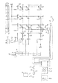
1つの行は、並列ラッチレジスタ2 内のその関連したビットを低レベルに設定し、残りのビットを高レベル設定することによって選択され、それによって、その行のためのトランジスタスイッチがオン状態にされる。レジスタ2 におけるデータはマイクロプロセッサ3 によって設定され、そのマイクロプロセッサ3 は、最初にデータを直列入力並列出力シフトレジスタ1 にロードし、その後、端子6 にパルスを与えることによってそれをレジスタ2 にストローブする。データは、その直列データ入力4 およびクロック入力5 によってレジスタ1 中にロードされる。レジスタ1 および2 は、それぞれmビットである。
【0013】
列の選択もまた、マイクロプロセッサ3 の制御の下で行われる。マイクロプロセッサ3 は、データ入力9 およびクロック入力10のそれぞれによって直列入力並列出力レジスタ7 にデータをロードし、その後、レジスタ7 におけるデータをストローブ端子11へのパルスによって並列ラッチレジスタ8 へ移動させる。列は、レジスタ8 におけるその関連したビットが高レベルのときに、そのトランジスタスイッチSCによって選択される。電流は、選択された行からランプLを通って列スイッチSCへ通り、その後、閉じられたスイッチ20を介して接地点へ流れる。レジスタ8 は接地端子(図示されていない)を有しており、それは、接地点あるいはトランジスタSCのエミッタのいずれかに接続されることができる。
【0014】
行選択期間TR 中、マイクロプロセッサ3 は、レジスタ8 をTA 秒毎に1回の割合で連続的に256回設定し、そこにおいてTA =TR /256である。これによって、観察者によって認められるように、各ランプの輝度は256の異なる値の任意の1つに設定されることができる。ランプが設定される輝度は、そのランプに特有のマイクロプロセッサメモリにおける位置Hに保持されたランプに特定のパラメータGの値に依存している。値Gの範囲は、1乃至255である。G=255である場合、ランプは、列選択期間TR 全体にわたってオン状態にされるように最大の輝度でオン状態にされる。G=1である場合、ランプは最小の輝度でオン状態にされる。
【0015】
一般的に、マイクロプロセッサ3 は、行xの選択期間中にGx,y の連続した期間TA だけレジスタ8 のビットyを高レベルに設定することによってランプLx,y (すなわち、行x、列yにおけるランプ)の輝度を制御し、ここにおいて、Gx,y は、ランプLx,y のメモリ位置Hx,y に記憶されたGの値である。従って、ランプを選択するためにレジスタ8 におけるビットが設定される時間の割合によって、そのランプの輝度が決定される。
【0016】
説明されたディスプレイモードにおける動作とは別に、図1および2のディスプレイはまた、光感知ユニット21の能力に依存して2つの初期設定モードの1つに設定されることができる。そのようなユニットが使用された場合、スイッチ26は位置27に設定され、スイッチ20は閉じられたままである。光感知ユニット21は、ランプLのマトリックスに向けられたビデオカメラであってもよい。ランプLは、全てのランプに対してGを255に等しく設定することによって全てが最大の輝度でオン状態にされる。ランプは、それらを加熱しないように0.1秒以下の短い期間オン状態にされる。ビデオカメラ21の出力はマイクロプロセッサ3 に伝送され、マトリックスの画像はメモリに記憶される。カメラ21からマイクロプロセッサ3 への伝送は、アナログ−デジタル変換器22および赤外線送信機23の補助によって行われ、赤外線送信機23は、デジタル化された画像データを光学通路24を通じて赤外線受信機25に伝送する。受信機25は、マトリックスを収容しているキャビネットに取付けられている。送信機23は、カメラもしくはその三脚に取付けられ、受信機に指向されている。カメラ21は、変換器22が必要でない場合にはデジタル式の静止した(スチール)カメラである。記憶された画像は、全てのランプの輝度読取りを得るためにマイクロプロセッサ3 によって解析される。輝度読取りはマイクロプロセッサ3 によって走査され、それによって、どのランプLの輝度が最も小さいかを決定し、この最も弱いランプの輝度が基準の輝度とされる。これに続いて、各ランプの輝度読取りは、そのメモリ位置HにあるランプのGの値を設定するためにマイクロプロセッサ3 によって使用される。Gの値は、次の式によって与えられる。
【0017】
G=(255×基準輝度)÷(ランプの輝度読取り値)
Gの値は、四捨五入されて最も近い整数にされる。これによって、初期設定処理が完了する。カメラは省くことができ、システムは、全てのランプが実質的に等しい輝度を有しているように見える状態で表示する準備ができている。弱いランプは、均一性を得るために強いランプよりも多くの電力を得る。ランプがオン状態にされ、それ故にそれに電力が与えられる時間の割合は、ランプのGの値に比例する。
【0018】
使用によるLEDランプの不均衡なフェーディングを補償するために、初期設定は例えば毎年1回等周期的に実行されることができる。カメラから受信された情報を解析するソフトウェアを簡単化するために、各ランプがそれ自体で順番にオン状態になり、ランプがオンであるときにカメラによって画像が撮影されるように測定方法を変更することができる。画像は、1秒につき数枚の割合で撮られることができる。その方法は、カメラの分解能が低い場合に、カメラが一時にマトリックスの1/4だけに向けられるように変更されることができる。画素を読取る際にサインの表面からの反射として現れる周囲光の効果を排除するために、システムは、それがオンであるときおよびオフであるときの両方に画素からの光を測定し、真の読取りのときとの差を得るように構成されることができる。
【0019】
別の方法として、カメラ21は、ラップトップコンピュータに接続されることができ、そのラップトップコンピュータのディスプレイスクリーンは、カメラによって見られた画像を示す。ラップトップコンピュータは、画素の光強度を解析し、後にメモリコンパートメントHに記憶されるためにディスプレイに送られるGの値を計算するために使用される。Gの値の伝送は、実質的にメモリHである媒体上にそれらを記録することによって行われることができる。
【0020】
別の選択肢として、通常のフィルムのカメラもしくはポラロイドカメラがGの値の設定に使用されることができる。2枚の写真が撮られ、1枚はランプが全てオンであり、もう1枚はそれらがオフの状態で撮られたものである。写真は、それらを読取るためのスキャナと、2枚の写真の間の差を算定し、Gの値を計算するためのパーソナルコンピュータとを使用して解析される。Gの値は、続いて非揮発性のタイプであることが好ましいメモリHに送られる。
【0021】
ディスプレイマトリックスはカラー用であり、そこにおいて、画素領域は幅広い範囲の異なったカラーの任意の1つに設定されることができる。この場合において、1つは赤、1つは緑、1つは青である3個のLEDが画素に対して使用される。3個のLEDは、共通のディフューザの後方に設けられることができる。その代りに、それらは近くに一緒に設けられることができ、それによって、一定の距離をおいて見られたときに、画素領域は3色の発光されたカラーが組合わされた1色のものであると眼が感じる。カラーマトリックスの行1の画素1に対して、3つの異なるカラーのLEDがL1,1 、L1,2 、L1,3 として行に沿って配線され、行1の画素2に対して、それらはL1,4 、L1,5 、L1,6 として配線される。前方の行2は、同じ原理を使用して配線される。画素の付勢の期間中、レジスタ8 におけるその3つの関連したビットが設定される期間は、Gの値だけでなく、画素に対して要求される色調を達成するために必要な3個の画素ランプの関連した強度を決定するメモリにおいて保持されている別の値にも依存して設けられる。従って、画素に対して要求される光出力Urgb は、その3個のLEDランプを以下のように駆動することによって達成される。
【0022】
赤ランプ: Nr =Gr ・Pr
緑ランプ: Ng =Gg ・Pg
青ランプ: Nb =Gb ・Pb
ここにおいて、Nr 、Ng 、Nb は、赤、緑、および青のランプがそれぞれ駆動されるTR の期間中の時間TA の数であり、Gr 、Gg 、Gb は、赤、緑、および青のランプのそれぞれのGの値であり、Pr 、Pg 、Pb は、それぞれが1以下であり、メモリにおいて保持され、カラー画素を発生するために必要とされる赤、緑、青の光の量をそれぞれ決定する。例えば、カラー画素が最大の強度の青緑色の光を発生するために要求された場合、Pr =0、Pg =1、Pb =1である。これまでは、赤ランプはカラーにおいて同一であり、同様に、緑ランプおよび青ランプにおいてもそうであると仮定されてきた。3色のランプの1以上のランプがカラーおよび強度の両方において不整合である場合について、後に説明される。
【0023】
初期設定期間中、カメラを光センサ21として使用する代りに、光電池を使用することが可能である。この場合において、各ランプは、光電池が光を受取ることによって順にオンにされ、ランプ光のデジタル読取りは、マイクロプロセッサのメモリに記録される。
【0024】
カメラあるいは光電池を使用した初期設定の代りに、光出力ではなくLEDの電流を測定することができる。この場合において、スイッチ20は開かれ、スイッチ26は端子28に設定される。各ランプLは、その行導体および列導体を選択することによって順にオンにされ、その電流の測定は、例えば1オームである抵抗30と、増幅器31と、アナログ−デジタル変換器32の補助によって行われる。測定結果は、ランプに関連したマイクロプロセッサ3 のメモリの位置に記憶される。全てのランプの電流が測定および記憶された後、どのランプが最も弱い電流を有しているかを決定するために測定結果が走査される。この最も弱い電流は、基準電流として確立される。その後、マイクロプロセッサは、以下のように与えられるGの値を供給するために使用される。
【0025】
G=(255×基準電流)÷(ランプの測定された電流値)
Gの値が与えられた後、スイッチ20は閉じ位置に戻され、表示の準備ができる。この状態において、システムは、ランプの不均衡な電圧降下およびトランジスタの電圧降下における変化によって生じたランプの輝度の変化を補償する。
【0026】
図2におけるシステムは、周囲光が弱くなったときに全てのランプを暗くするように構成されている。デジタル出力を有する光センサ40は、周囲光を測定し、そのデジタル値をマイクロプロセッサ3 に伝送するように構成されている。例えば、夕暮れあるいは夜等において感知された周囲光の低い値に対して、マイクロプロセッサ3 は、各行とその次の行の駆動の間に時間遅延を導入する。これによってディスプレイの光出力は減少するが、ランプの関連した輝度を変更することはなく、それは依然としてGの値によって制御されている。
【0027】
図1および2におけるランプLは、より電力を与えるために直列に一緒に接続された幾つかのLEDをそれぞれ具備している。その代りに、それらは、LEDとは異なるタイプであってもよい。例えば、それらはタングステンフィラメントランプであってもよい。タングステンランプを選択する簡単な方法は、図3のbにおいて図示されているように、そのそれぞれに通常のダイオードDを直列に提供することである。タングステンランプの光出力は、時間と共に徐々に弱まる。これは、長期にわたって使用した後にバルブの内部表面上に黒い被覆が形成されるからであり、しばしばオン状態にされていたバルブは、そうでないバルブよりも暗くなる。
【0028】
図4において、本発明の別の実施形態が示されている。光学手段によるランプの整合に関連したこの動作は、図2のものと同じである。ここにおけるランプは定電流で駆動され、その大きさは、温度センサ41の出力に従って変化するように構成されている。温度センサ41はディスプレイ上に設けられ、それによって、LEDと同じ周囲温度をさらされる。LEDの周囲温度は、LEDあるいはその近隣に電力が与えられないときのLEDの温度のことである。デジタルで示されることができる温度センサ41の出力は、マイクロプロセッサ3 に供給される。
【0029】
マイクロプロセッサ3 は、測定された温度ta に従って4ビットのレジスタ54を設定するように構成される。ta が、例えば50℃等の所定のしきい温度tc 以下であるとき、レジスタ52における値は15に設定される。測定された温度ta がtc 以上に上昇すると、15よりも低い値がマイクロプロセッサ3 によってレジスタ52に設定される。レジスタ52の出力はデジタル−アナログ変換器53に供給され、その出力は順に利得が1の電力増幅器54に供給される。従って、トランジスタCCのベースに与えられた電圧は、マイクロプロセッサ3 によって制御される。列Cが選択されたとき、そのトランジスタCCは、LEDの電圧降下とは関係なく、増幅器54の出力電圧に依存し、それによって、感知された温度ta に従って調整される定電流を関連した抵抗50と共に選択されたLEDに配る定電流装置として機能する。抵抗50の値は、レジスタ52が15に設定されたときに、LED電流がLEDの製造業者によって許容され得る限りにおいて最大の大きさになるように選択される。tc 以上の感知された温度に対して、レジスタ52における値は、LED接合部の温度が所定の制限tu 以上に上昇せず、LED製造業者によって定められた最大の接合部温度の定格(典型的に110℃)を超過しないように選択された最も高い値に設定される。この方法において、サインの日中の輝度は、一方ではLED製造業者による最大の電流および温度の定格内に維持されながら自動的に最大にされる。1例として、マイクロプロセッサ3 は、ta がtc を超過したときに、次の式に従ってレジスタ52の内容Yを設定するように構成されることができる。
【0030】
Y=15−a・(ta −tc )
ここにおいてaは、0.25程度の定数である。
【0031】
カメラ21を使用して、図4の構成は、図2に関連して説明されたものと同じ方法で全てのランプに等しい光出力を与えるように設定されることができる。この構成は、列から列への定電流の変化の影響、異なるLEDの初期の光の効率による変化の影響、および劣化のために生じる変化の影響を補償する。
【0032】
図2の構成において、ランプがLEDタイプである場合、マイクロプロセッサ3 は、センサ41によって感知された温度が高いときにランプLがオン状態にされる時間の割合を減少し、それによってLED接合部の温度が製造業者の定格を超過することを防ぐように構成されることができる。時間の割合の減少は、夜間にディスプレイを暗くすることに関連して前述されたように、ある行の駆動と次の行の駆動との間に遅延を導入することによって達成されることができる。
【0033】
図2および図4の両方に適用可能な本発明の別の実施形態において、マイクロプロセッサ3 は、辺りが暗くなるにつれてサインの輝度を暗くするだけでなく、サインの表面上に直接強力な日光が当たる等の極端な周囲光の状況の下でサインの全体の輝度を増加させるために光センサ40を使用するように構成される。マイクロプロセッサ3 は、強力な周囲光を検出する際に、ランプが等しい光出力を有するようにランプを駆動するのを止め、その代りに、ランプの最大の輝度を達成するために期間TR 全体にわたって各ランプを駆動するか、あるいはランプの輝度が例えば2等の所定の係数だけ他の任意のランプの輝度を超過しない最大の期間にわたって各ランプを駆動するように構成される。この場合において、均一性は、最大の全体輝度のために完全にあるいは部分的に犠牲にされるが、それは周囲光が極端な場合だけである。周囲光が低下したとき、マイクロプロセッサ3 は、ランプの輝度が等しくなるように設定し始める。
【0034】
図2および図4の構成におけるランプは、ディスプレイマトリックスのランプである必要はない。それらは計器ディスプレイパネルのランプであってもよい。計器パネルのランプは、各グループがそのグループに特有の輝度に設定されたランプを有している異なったグループであることもある。カメラ21を使用して第1のグループのランプを初期設定する期間中の場合において、最高の輝度を有することを要求されたグループは、最大の輝度でオン状態にされ、グループ内のどのランプが最も弱いかを決定し、その輝度は、前述されたように基準輝度とされる。その後、グループ内のランプのGの値は、ランプに等しい輝度を与えるように設定される。これに続いて、残りのそれぞれのグループに対してグループ内の各ランプは、次の式によって与えられたGの値を割当てられる。
【0035】
G=[(255×基準輝度)÷(ランプの輝度読取り値)]×RBn
ここにおいて、RBn は、基準輝度に関するグループnのランプの輝度の要求された割合である。RB1 、RB2 、RB3 等の定数の値は、メモリにおいて永久的に保持され、計器パネルの設計者によって最初に選択される。設計者はまた、各ランプがどのグループであるかを特定し、この情報はメモリに永久的に記録される。
【0036】
計器パネルは、点灯されたときにディフューザ上にプリントして可視状態にする後方ランプをそれぞれが設けられた予めプリントされた光ディフューザを含んでいる。この場合において、全ての後背照明されたディフューザは1つのグループとして扱われることができ、初期設定の結果として、全てのディフューザが別のグループの輝度に関して予め定められた等しい輝度を有することができる。パネルのランプは、全てが同じタイプである必要はなく、それらは、全てが同じ値の限流抵抗器を有している必要はない。
【0037】
また別の実施形態において、図2および4の構成のいずれかを使用して、本発明は、それ自体はカラーにおいて整合されていないLEDランプを使用してカラーが整合されている画素を有するディスプレイを提供するように構成されている。この実施形態は、緑のLEDランプがカラーにおいて整合されていないということに基づいて、RGBカラーディスプレイマトリックスに関して説明される。この実施形態において、強度係数がPg である緑色だけがカラー画素に対して必要とされるとき、緑色のLEDランプをオンにする代りに、
Ng =Gg ・Pg 期間TA
とし、前述のように行選択時間TR の期間中、制御によって赤ランプもまたオン状態にされて
Nrgs =Gr ・Pg ・Zrg期間TA
となり、ここにおいて、Zrgは、緑色のLEDランプのカラー補正係数であり、全ての画素に対して同じ主波長(すなわち、同じ感知された色)の緑色を達成するために緑色のLEDランプによって放射された光に加えられなければならない赤い光の割合を特定するものであり、非揮発性メモリに保持されている。このような方法で赤い光を加えて全ての画素に整合させるために、それらのランプが同じ温度であるときには、それらが緑色にオンされたときに同じ外見的な色を有する。
【0038】
準備の期間中、カラーカメラ21はディスプレイに向けられ、画素に対するGr の値は、光の測定のためのカメラの赤のチャンネルを使用して設定される。同様に、Gg の値は緑のチャンネルを使用して設定され、Gb の値は青のチャンネルを使用して設定される。ランプの強度を均一にした後、画素に対するZrgの値は以下のように設定される。緑色のLEDランプは、同じ光強度Wgeで一時に1個、一時に数個、あるいは同時に全てがオンにされる。各画素に対して、緑色のLEDランプから発せられる赤い光の強度Wrgがカメラの赤チャンネルを使用して測定され、記録される。その後、Wrgの値が走査され、緑色のLEDランプが最も赤い光を発生する画素に対応してWrg(max)を捜す。このランプのカラーは、基準カラーと見なされる。各画素に対して、Zrgの値は、
Zrg=[Wrg(max)−Wrg]/Wge
によって評価され、その後、それは非揮発性メモリに記憶される。この式によって、緑色にオンされた全ての画素は、基準カラーの赤のランプ対緑のランプの比率と同じ比率Wrg(max)/Wgeを有する光を放射する。
【0039】
青は、カラーにおいて緑色のランプを整合するために赤の代りに使用されることができる。選択的に、青は、選択された量以上の赤を有する緑色のランプを修正するために使用されることができ、赤は、緑色のランプの残りを訂正するために使用されることができる。画素の整合において、マトリックスのランプと同じ手段によって測定された基準強度および基準カラーのランプは、選択されたランプのマトリックスを基準として使用する代りに、ランプのマトリックスが設定される基準として使用されることができる。この方法で、製作された全てのディスプレイが共通の基準に整合されることができる。カラーの整合は、それぞれの場合において緑を使用して、赤のランプおよび青のランプに適用されることができる。
【0040】
上に説明されたカラー修正システムは、モノクロームディスプレイの画素のカラーを整合するために使用されることもできる。すなわち、例えば、黄色のLED単色ディスプレイの画素は、多数の黄色のLEDによって囲まれた赤のLEDをそれぞれ設けられ、赤のLEDは、上述の方法で画素の色調を標準化するために使用され、一定の距離を隔てて見たときに全ての画素が黄色の同じ明確なシェードになるようにする。
【0041】
LEDランプがカラーの劣化、すなわち、使用によるカラーの変化を受けた場合、ランプは一定時間の後にカラーを適切に整合することを中止する。カラーの劣化によるカラーの不整合は、ときどき再度準備することによって減少されることができる。
【0042】
LEDマトリックスは、ランプの強度において、表示されたメッセージが変わる際の過渡的な熱効果によって生じたダイナミックな変化を受ける。温度が上昇するにつれて、光出力は係数Jだけ低下する。Jは、あるLEDに対して1℃につき.01程度である。
【0043】
本発明のさらに別の実施形態として、ディスプレイシステムは、以下のように温度依存のダイナミックな強度係数によって各LEDランプへの駆動を変更することによってダイナミックな変化を修正するように構成される。
【0044】
E=1/(1−J・Δt)
ここにおいて、Δtはランプの温度tの変化である。ランプの温度は、その接合部における温度である。
【0045】
図2における基本的な構成を使用して、各ランプに対するEの値は、準備期間中におけるランプが全て同じ温度tpであるときと、表示の期間中におけるランプが異なる温度であるときの両方において電流Iを測定することによって決定される。これは以下に説明される。スイッチSR,SCが、例えば無視できる程度の“オン”抵抗を有するMOS電界効果トランジスタ等の理想的なスイッチであると仮定し、抵抗30の測定の影響を考慮しないと、選択されたランプの電流Iは、次式により与えられ、
I=(VD −VL )/RS
ここにおいて、VL は、ランプの両端の電圧である。VD およびRS の値は、温度とは関係なく、それによって、ランプの温度の変化Δtによるランプの電流の変化Δlは、次式によって与えられる。
【0046】
Δl/Δt=−(ΔVL /Δt)/RS
LEDランプに対して、(ΔVL /Δt)は定数B(1℃につき約−.002ボルトに等しい)であるので、
Δl/Δt=−B/RS
となり、この式から、
Δt=Δl・RS /B
となり、Eに対する式においてこれを置換すると、次のようになる。
【0047】
E=1/(1+Δl・RS ・J/B) …………………………(1)
図2における構成を使用して各ランプに対する補正係数Eを評価および使用する方法が以下のように行われる。準備に先行して、ディスプレイは、全てのランプLが同じ一定の温度tp に到達することができるように1分以上の時間消灯される。その後、Gの値は、例えば前述のようにカメラ21を使用し、ランプの温度を変えないように短い間だけランプが駆動されるように注意して設定される。Gの値が設定された後、スイッチ20は開かれ、スイッチ26は位置28に設定され、各ランプLはその温度を変えないように短い間だけ順にオンにされ、その電流Ip は測定されて非揮発性メモリに記録される。ディスプレイの準備が実行された温度tp は、センサ21から読取られ、非揮発性メモリに記録される。スイッチ20は、MOS電界効果タイプであることが好ましい。
【0048】
表示の期間中、スイッチ26は位置28に設定され、行Rが選択される度に以下の方法が実行される。
【0049】
a)スイッチ20が開かれ、行の各ランプの電流Iが急速に測定され、一時的に記録される。これは、レジスタ8 に沿って“1”をシフトして行われる。測定が急速であるために、ランプからの結果的な光は非常に弱く見ることができない。
【0050】
b)行における各ランプに対して、Eの値がマイクロプロセッサ3 によって以下の式から計算され、
E=1/{1+[I−Ip ]・Rs ・J/B}………………………(2)
一時的に記憶される。この式は、式(1)から得られる。
【0051】
c)スイッチ20がマイクロプロセッサ3 によって閉じられ、行は、表示するために、Gの代りに使用される値A・E・Gで各ランプに対して駆動される。係数Eを含むことによって、ランプ間の温度差による輝度の不整合は排除される。係数Aは、全てのランプに対して同じである。Aは、A・Eが1を超えないように選択される。例えば、それは0.5になるように選択されることができる。
【0052】
上述のプロセスによって、光出力は、周囲温度およびランプ間の温度差の両方とは関係がなくなる。
【0053】
所定のLEDに対するJ/Bの値は、温度tp におけるランプの電流Ip および輝度Wp を測定し、その後、ランプがその(接合部)温度をある未知の値tu に上昇させるように数秒間強力にランプを駆動し、その後、その未知の温度における電流Iu および輝度Wu を測定することによって準備の終わりにおいて決定されることができる。値は、以下のように相関しており、
1−Wu /Wp =J・(tu −tp )
(lu −lp )・Rs =B・(tu −tp )
これから、
J/B=(1−Wu /Wp )/(lu −lp )・Rs
となる。
【0054】
J/Bに対する値は、この最後の式から計算される。J/Bは、各ランプに対して個々に決定および記憶されることができる。
【0055】
上述のプロセスの変形として、ランプの温度の差のために生じるランプの輝度の変化を排除しながら、ディスプレイの輝度を周囲温度の上昇と共に減少させることが可能である。この場合において、以下の値E' が、上述のステップ(b)におけるEの代りに使用され、
E' =
1/{1+[l−lp +(ta −tp )・B/Rs ]Rs ・J/B}…(3)ここにおいて、ta は、表示の期間中にセンサ41から読取られた周囲温度値である。[l−lp +(ta −tp )・B/Rs ]における第3項は、ディスプレイの周囲温度がtp からta へ変化したときのランプの電流への影響を示している。
【0056】
LEDマトリックスは、ダイナミックな接合部の温度の変化によって生じたランプのカラーのダイナミックな変化を受ける。この効果は、緑および黄色のランプではより顕著に現れる。これらによって、温度が上昇するに従ってそれらのカラーが赤に変わる。
【0057】
強度の整合、ダイナミックな強度整合、カラー整合、およびダイナミックなカラーの整合を提供する本発明の1実施形態が、1つのカラー画素につき、1色に1つずつ、合計3個のLEDを有する図2の構成を使用してRGBディスプレイに関して以下に説明される。カラー整合は、緑のランプに対してのみ必要とされると仮定される。この場合において、カラー画素は以下のように駆動され、
Nr =Er ・A・[Gr ・Pg ]・[1+Zrg+Zrgd ]
Ng =Eg ・A・[Gg ・Pg ]
Nb =Eb ・A・[Gb ・Pb ]
ここにおいて、Er 、Eg 、Eb は、画素の赤、緑、および青のランプのそれぞれに対するEの値である。新しい項Zrgd は、ダイナミックなカラー補正係数であり、以下のように与えられる。
【0058】
Zrgd =(ta +tmr−t)・Q
ここにおいて、tmrは、接合部の温度の最大の予測された温度の上昇が周囲温度ta を超過した場合のための例えば50℃等の設計上の許容誤差であり、ここにおいてtは、前述のように、ランプの温度である。Qは、その温度が1℃上昇したときに生じる、緑のランプによって発生された緑の光に対する赤の光の割合の変化を定める定数である。その温度tが上昇するにつれ、緑色のランプはより赤の成分を発生するが、Zrgd によって、赤いランプはより少なくなり、温度に関係なく赤対緑の全体の比率を維持する。Zrgd は、以下のように示される。
【0059】
Zrgd =[(ta −tp +tmr)−(t−tp )]・Q
ランプの温度の変化Δtは、ランプの電流の変化Δlに関連しているので、
Δt=Δl・Rs /B
となり、従って、(t−tp )は置き換えられることができ、
Zrgd =(ta −tp +tmr)・Q−(I−Ip )Q・Rs /B
となり、そこから、
Zrgd =
[(ta −tp +tmr)・S・B/Rs ]−(I−Ip )・S …(4)
となり、ここにおいて、
S=Q・Rs /B
である。
【0060】
画素に対するSの値は、その接合部の温度がtp であるときのその電流Ip 、その緑色の光Wgp、およびその赤の光Wrgp を準備時間に決定するために緑のランプを点灯することによって決定されることができ、その後、接合部が高い温度tu であるときのその電流Iu 、その緑色の光Wgu、およびその赤の光Wrgu を決定することができる。Sの値は、
S=[Wrgu /Wgu−Wrgp /Wgp]/(lgu−lgp)
の式から計算され、非揮発性メモリに記憶される。式中の[Wrgu /Wgu−Wrgp /Wgp]は、2組の測定結果の間の赤い光対緑の光の比率における変化である。
【0061】
画素に対するZrgd の値は、式(4)から計算される。式(4)における[(ta −tp +tmr)・S・B/Rs ]中の係数は徐々に変化するため、1分に1度評価されることができる。別の係数(I−Ip )・Sは10ミリ秒毎に計算され、それはZrgd の値である。
【0062】
その代りに、温度と共に減少する赤い光を加える代りに、温度と共に増加する青い光を画素に加えることによって、緑のダイナミックなカラー訂正が行われることができる。
【0063】
RGB表示は、強度の劣化による不均衡と同様に、カラーの劣化による不均衡を減少するために、例えば1年に1度、再準備されることができる。
【0064】
今まで説明されてきたダイナミックな補償は、ある準備時間と次の準備時間との間に生じる劣化のためにランプの電圧−電流特性が著しく変化することのないディスプレイに適用することができる。
【0065】
低下と共に電圧−電流特性の著しい変化を示すタイプのランプが使用された場合、頻繁に準備することなくダイナミックな補償の正確度における低下の影響を最小にするために、システムは、例えば1日に1回午前3時にそれ自体で反復的に試験するように構成される。この時に、ディスプレイは、全てのランプが温度センサ41によって与えられた同じ温度tm に冷却されるように1分以上消灯される。温度tm は記録され、各ランプ毎にランプ電流Im が測定および記録される。続く表示期間中、ダイナミックな強度補正のステップ(b)において、Im が式(2)あるいは選択的に式(3)のIp の代りに使用される。Im はまた、ダイナミックなカラー補正係数Zrgd のために式(4)においてもIp の代りに使用される。特典として、システムは、この場合において再度準備せずにランプにおける劣化を検出することができる。システムは、Im をIp と比較し、
Im <[Ip +(B/R)・(tm −tp )]
である場合、ランプの内部抵抗は増加しており、劣化を表す。ランプの劣化の不均衡によって生じるランプの輝度の差を減少するために、ランプの輝度は、式の両側の間の差に依存した量だけシステムによって強められることができる。
【0066】
ΔV=−Δl・Rs であるので、ランプの電流の代りにランプの電圧を測定することによってダイナミックな補償を行うことが可能である。図4の構成において、ランプを駆動し、その列のスイッチSSを閉じることによって、増幅器31およびアナログ−デジタル変換器32を介してランプ電圧を読取ることができる。スイッチSRおよびSSは、この場合において、最小な電圧降下を有するMOS電界効果タイプであることが好ましい。
【0067】
図2および図4の構成のそれぞれに対して、カメラセンサ21をフォトトランジスタ等の単一のフォトセンサと置換することができ、その出力は、1メガサイクルの水晶等の同調された回路に供給され、それは、復調器に供給する。この場合において、準備期間中の測定において、ランプLは、1秒につき100万パルスのパルス列で一時にそれぞれ1個ずつ点灯される。
【0068】
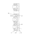
ランプLは、一緒に接合されたタイル上に設けられ、各タイルは、例えばランプの16×16のマトリックスを有している。図5において図示されているタイル60は、印刷回路板61の背面にはんだ付けされたランプLと、板の前面に設けられた半透明の光ガイドシート62とを含んでいる。シート62は、各ランプLと向かい合った光拡散部63と、シート62からの光を受けるためにタイルの中心に設けられたフォトトランジスタ64に向かい合った光拡散部65とを有している。拡散部63,65 は、シート62においてファセット、溝、あるいは粗面によって構成されている。フォトセンサ64の出力は、適切な電子装置を介して1メガサイクルだけ通過させるフィルタに供給される。毎日午前3時に、システムは、1秒につき100万パルスで順に各ランプを点灯(付勢)し、そのような点灯(付勢)期間中にフィルタ回路の出力を測定し、測定結果を記録し、同じ方法で行われた先行する測定に関して、劣化によってランプの光出力が変化したか否かを確定し、光の検出された変化を補正するように構成される。センサ64は、タイルから全てのタイルに共通であるセンサに光を伝送する光ファイバガイドと置換されることもできる。代りに、各タイルは、それに近くないタイル上のランプを感知するためにそれぞれ使用される2つの光ファイバガイドを設けられることもできる。この手段によって、各ランプ拡散部63を適切に個々に調整することができるだけでなく、タイル上のランプ位置とは関係なくランプの感知を達成することができ、それよって、ランプと拡散部65との間の光伝送における差を補償するための異なる増倍係数を使用せずに初期設定するように感知システムを使用することができる。全ての光ファイバガイドのための共通のセンサは、赤、緑、および青の光の成分を別個に測定するように構成された1個の装置であってもよい。
【0069】
シフトレジスタ1 および7 は、マイクロプロセッサ3 もしくはそれに接続された任意の外部メモリからの直接のバイトあるいはワードで駆動レジスタ2 および8 を迅速に負荷するように構成されたゲートに置換されることができる。
【0070】
表示のために必要な画素を特定するPr 、Pg 、Pb 等の情報は、ここでは指令情報として分類される。対照的に、温度、電流、Gの値、Bの値、Zrgの値、Eの値等のランプの特性に関する情報あるいはパラメータは、本明細書では物理的情報として分類される。
【図面の簡単な説明】
【図1】本発明によるランプマトリックスディスプレイの構成を示す図。
【図2】ディスプレイの制御回路図。
【図3】ディスプレイにおいて使用できる2種類のランプの概略図。
【図4】ディスプレイの別の制御回路図。
【図5】ランプからの光を感知するための構造の断面図。[0001]
BACKGROUND OF THE INVENTION
The present invention relates to enhancing the appearance of a display matrix in which each pixel comprises an LED lamp. It can also be applied to matrix displays that use other types of lamps, such as incandescent filament lamps, and also to display panels that use lamps that do not need to be arranged in a uniform manner.
[0002]
[Prior art]
The problem in designing the LED lamp matrix is to achieve uniformity so that all lamps give the same light output. The light output of a new LED at a given temperature depends on its light efficiency measured as light intensity in unit current and the operating current. Further, the LED is subjected to a decrease in strength such as fading due to long-term use.
[0003]
For most types of LED lamps, the efficiency of light, often expressed in the form of emission intensity at 20 mA, can vary from sample to sample in a ratio of about 5: 1. For some types, the diodes are screened from the production line such that the maximum light efficiency from sample to sample versus the minimum light efficiency is a low ratio, such as 2: 1.
[0004]
In a multiplex driven LED matrix, the current is normally limited in each LED by a resistor in series with the LED when it is turned on, and the matrix avoids reverse breakdown of the LED and reduces power consumption. It is preferably driven from a 5 volt supply to maintain. The current I in the selected LED in such a case is given by
I = (5-VL) ÷ Rs
Where VLIs the forward voltage drop of the LED and RsIs the resistance value of the current limiting resistor. VLCan vary from 1.8 volts to 3 volts for some types of LEDs, and using such types of LEDs, the current I is the maximum value 3.2 / RsTo the
[0005]
Yet another factor affecting the uniformity of the LED display matrix is that not all of the LED junctions are at the same temperature. An LED that is on or previously on is hotter than one that was off. The temperature difference between the hottest and coldest joints at any one time is on the order of 50 ° C. This represents a further 2: 1 mismatch in intensity, as the light intensity of the LED drops by 1% per 1 ° C. This effect is dynamic. The time constant of the temperature change at the junction is on the order of 1 second for the LED itself and typically on the order of tens of seconds for the heat sink that is the printed circuit board.
[0006]
Not only is there a mismatch effect in intensity, but there is also a color mismatch effect. LED lamps are initially mismatched in colors on the order of 11 nanometers at some green LED wavelengths when received from the manufacturer. Further, the LEDs are subject to dynamic color mismatch due to the lamp dynamic temperature mismatch. Furthermore, LEDs are subject to color degradation, i.e. color changes due to long-term use, which itself causes color mismatch, because the lamp is not used uniformly, In any case, it is not guaranteed to deteriorate at the same rate.
[0007]
[Problems to be solved by the invention]
In television and photographic technology, a 1.05: 1 intensity mismatch ratio is established as recognizable when the green color mismatch is 0.7 nanometers. The above changes in LED operation are more widespread, thus preventing achieving high quality images with the LED matrix. It is an object of the present invention to provide an LED display matrix in which all lamps give the same light output, are matched in intensity and color, and are not affected by dynamic effects, and these results are reduced to a low cost matrix drive. Is achieved by the system. Another object of the present invention is to configure the display to be as bright as possible during daylight while maintaining within the maximum current and junction temperature ratings specified by the LED manufacturer.
[0008]
[Means for Solving the Problems]
The present invention provides a control system for measuring the characteristics of a lamp, measuring ambient light striking the lamp, and also measuring the ambient temperature of the lamp in some embodiments with the aid of a video or digital camera. To achieve. These measurement results are used by the control system to optimize the appearance of the display. In one embodiment, the difference in light output between lamps is minimized to a predetermined limit for all ambient light intensities. Exceeding this lamp uniformity limit, lighting is partially or totally sacrificed to achieve maximum brightness. The control system changes the brightness of each lamp individually by changing the ratio of the time that the bits of the register that selects the lamp are set. In one embodiment, the brightness of the lamp also depends on a constant current circuit that sends a current to the lamp that depends on the ambient temperature of the lamp.
[0009]
In another embodiment, for each pixel of the display, the color of the first lamp of the pixel is adjusted by turning on the lamp of the second different color pixel, so that all in color Pixels are aligned. In another embodiment of the invention, electrical characteristics such as current are continuously measured during display for each lamp. This measurement result is used to reduce lamp-to-lamp mismatch in brightness and color resulting from lamp imbalance temperature.
[0010]
DETAILED DESCRIPTION OF THE INVENTION
In FIGS. 1 and 2, an embodiment of the present invention is shown comprising a display matrix having m rows and n columns of lamps L. FIG. The lamp L comprises a light emitting diode whose anode is connected to the row conductor R and whose cathode is connected to the column conductor C, as shown in FIG. When the lamp L is lit, it constitutes a light emitting area. When the lamp L is not lit, it constitutes a dark area as opposed to a light emitting area. The lamp is installed on one or more panels not shown.
[0011]
Information is short period TRAre displayed on the matrix by sequentially driving each row R, and the driving is continuously performed in the order of 1, 2, 3,... M, 1, 2, 3,. Repeated. The period T during which one row is drivenRWithin, the selected lamps L in the row are illuminated by turning on the transistors SC of their associated row conductor C. TRIs about 0.1 milliseconds.
[0012]
A row is selected by setting its associated bit in
[0013]
Column selection is also made under the control of the
[0014]
Row selection period TRMicroprocessor 3 sets register 8 to TASet 256 times continuously at a rate of once per second, where TA= TR/ 256. This allows the brightness of each lamp to be set to any one of 256 different values, as recognized by the observer. The brightness at which the lamp is set depends on the value of the parameter G specific to the lamp held at position H in the microprocessor memory specific to that lamp. The range of the value G is 1 to 255. If G = 255, the lamp is in the column selection period TRIt is turned on at maximum brightness so that it is turned on throughout. If G = 1, the lamp is turned on with minimal brightness.
[0015]
In general, the
[0016]
Apart from operating in the described display mode, the display of FIGS. 1 and 2 can also be set to one of two default modes depending on the capabilities of the
[0017]
G = (255 × reference brightness) ÷ (lamp brightness reading)
The value of G is rounded to the nearest integer. Thereby, the initial setting process is completed. The camera can be omitted and the system is ready to display with all lamps appearing to have substantially equal brightness. A weak lamp gets more power than a strong lamp to achieve uniformity. The percentage of time that the lamp is turned on and is therefore powered is proportional to the G value of the lamp.
[0018]
In order to compensate for the unbalanced fading of the LED lamps due to use, the initial setting can be carried out, for example, once a year on a regular basis. To simplify software that analyzes information received from the camera, the measurement method has been changed so that each lamp is turned on in turn and the camera takes an image when the lamp is on. can do. Images can be taken at a rate of several per second. The method can be modified so that when the camera resolution is low, the camera is directed to only a quarter of the matrix at a time. To eliminate the effect of ambient light that appears as reflections from the surface of the sign when reading the pixel, the system measures the light from the pixel both when it is on and when it is true It can be configured to obtain the difference from when reading.
[0019]
Alternatively, the
[0020]
Alternatively, a normal film camera or polaroid camera can be used to set the G value. Two pictures were taken, one with all the lamps on and the other with them off. The photos are analyzed using a scanner for reading them and a personal computer for calculating the difference between the two photos and calculating the value of G. The value of G is then sent to the memory H, which is preferably a non-volatile type.
[0021]
The display matrix is for color, where the pixel area can be set to any one of a wide range of different colors. In this case, three LEDs are used for the pixel, one red, one green and one blue. Three LEDs can be provided behind a common diffuser. Instead, they can be placed close together so that when viewed at a certain distance, the pixel area is of one color combined with three emitted colors. The eyes feel when there is. For
[0022]
Red lamp: Nr= Gr・ Pr
Green lamp: Ng= Gg・ Pg
Blue lamp: Nb= Gb・ Pb
Where Nr, Ng, NbT, where the red, green and blue lamps are respectively drivenRTime T during the periodAThe number of Gr, Gg, GbIs the value of G for each of the red, green and blue lamps and Pr, Pg, PbAre each 1 or less and determine the amount of red, green, and blue light, respectively, that is held in memory and is required to generate a color pixel. For example, if a color pixel is required to generate blue-green light of maximum intensity, Pr= 0, Pg= 1, Pb= 1. So far it has been assumed that red lamps are identical in color, as well as green and blue lamps. The case where one or more of the three color lamps are mismatched in both color and intensity will be described later.
[0023]
Instead of using the camera as the photosensor 21 during the initial setting period, a photocell can be used. In this case, each lamp is turned on in turn as the photovoltaic cell receives light, and a digital reading of the lamp light is recorded in the memory of the microprocessor.
[0024]
Instead of the initial setting using a camera or photocell, the LED current can be measured rather than the light output. In this case, switch 20 is opened and switch 26 is set to
[0025]
G = (255 × reference current) ÷ (measured current value of the lamp)
After the value of G is given, the
[0026]
The system in FIG. 2 is configured to darken all lamps when ambient light is weakened. The
[0027]
The lamps L in FIGS. 1 and 2 each comprise several LEDs connected together in series to provide more power. Alternatively, they may be of a different type than the LED. For example, they may be tungsten filament lamps. A simple way to select a tungsten lamp is to provide a normal diode D in series with each one, as illustrated in FIG. 3b. The light output of the tungsten lamp gradually decreases with time. This is because after a long period of use, a black coating is formed on the internal surface of the bulb, and valves that are often turned on are darker than those that are not.
[0028]
In FIG. 4, another embodiment of the present invention is shown. This operation related to the alignment of the lamp by the optical means is the same as that of FIG. The lamp here is driven by a constant current, and the size thereof is configured to change according to the output of the
[0029]
The
[0030]
Y = 15−a · (ta-Tc)
Here, a is a constant of about 0.25.
[0031]
Using the
[0032]
In the configuration of FIG. 2, if the lamp is of the LED type, the
[0033]
In another embodiment of the invention applicable to both FIG. 2 and FIG. 4, the
[0034]
The lamps in the configurations of FIGS. 2 and 4 need not be display matrix lamps. They may be instrument display panel lamps. The lamps on the instrument panel may be different groups, with each group having a lamp set to a brightness specific to that group. In the case of initializing lamps of the first group using the
[0035]
G = [(255 × reference luminance) ÷ (lamp luminance reading)] × RBn
Where RBnIs the required percentage of the brightness of the group n lamps with respect to the reference brightness. RB1, RB2, RBThreeThe constant values such as are kept permanently in memory and are initially selected by the instrument panel designer. The designer also identifies which group each lamp is in and this information is permanently recorded in memory.
[0036]
The instrument panel includes pre-printed light diffusers each provided with a rear lamp that, when lit, prints on the diffuser to make it visible. In this case, all back illuminated diffusers can be treated as one group, and as a result of the initialization, all diffusers can have a predetermined equal brightness with respect to the brightness of another group. The panel lamps need not all be of the same type and they need not all have current limiting resistors of the same value.
[0037]
In yet another embodiment, using any of the configurations of FIGS. 2 and 4, the present invention provides a display having pixels that are color-matched using LED lamps that are not themselves color-matched. Configured to provide. This embodiment is described with respect to an RGB color display matrix based on the fact that green LED lamps are not matched in color. In this embodiment, the intensity factor is PgInstead of turning on the green LED lamp when only green is needed for color pixels,
Ng= Gg・ PgPeriod TA
And row selection time T as described aboveRDuring this period, the red lamp is also turned on by the control.
Nrgs= Gr・ Pg・ ZrgPeriod TA
Where ZrgIs the color correction factor of the green LED lamp and is added to the light emitted by the green LED lamp to achieve the same dominant wavelength (ie the same perceived color) green for all pixels. It specifies the percentage of red light that must be kept in non-volatile memory. To add red light in this way to match all pixels, when the lamps are at the same temperature, they have the same appearance color when they are turned on in green.
[0038]
During the preparation period, the
Zrg= [Wrg(Max) -Wrg] / Wge
Is then stored in non-volatile memory. According to this equation, all pixels turned on green will have the same ratio W as the ratio of the reference color red lamp to the green lamp.rg(Max) / WgeEmits light having
[0039]
Blue can be used instead of red to match a green lamp in color. Optionally, blue can be used to correct a green lamp that has more than a selected amount of red, and red can be used to correct the rest of the green lamp . In pixel matching, the reference intensity and reference color lamps measured by the same means as the matrix lamps are used as the basis for which the lamp matrix is set, instead of using the selected lamp matrix as a reference. be able to. In this way, all manufactured displays can be matched to a common standard. Color matching can be applied to the red and blue lamps using green in each case.
[0040]
The color correction system described above can also be used to match the color of the pixels of a monochrome display. That is, for example, the pixels of a yellow LED monochromatic display are each provided with a red LED surrounded by a number of yellow LEDs, and the red LED is used to standardize the color of the pixel in the manner described above, All pixels should have the same clear shade of yellow when viewed at a certain distance.
[0041]
If the LED lamp undergoes color degradation, i.e., a color change due to use, the lamp stops properly aligning the color after a certain time. Color mismatch due to color degradation can be reduced from time to time by preparing again.
[0042]
The LED matrix undergoes dynamic changes in lamp intensity caused by transient thermal effects as the displayed message changes. As the temperature increases, the light output decreases by a factor J. J for each LED at 1 ° C. It is about 01.
[0043]
As yet another embodiment of the present invention, the display system is configured to correct for dynamic changes by changing the drive to each LED lamp with a temperature dependent dynamic intensity factor as follows.
[0044]
E = 1 / (1-J · Δt)
Here, Δt is a change in the lamp temperature t. The lamp temperature is the temperature at the junction.
[0045]
Using the basic configuration in FIG. 2, the value of E for each lamp is both when the lamps are all at the same temperature tp during the preparation period and when the lamps are at different temperatures during the display period. Determined by measuring the current I. This is explained below. Assuming that the switches SR, SC are ideal switches, such as MOS field effect transistors having negligible “on” resistance, for example, the current of the selected lamp is considered without taking into account the measurement effect of the
I = (VD-VL) / RS
Where VLIs the voltage across the lamp. VDAnd RSThe value of is independent of temperature, so that the change in lamp current Δl due to the change in lamp temperature Δt is given by:
[0046]
Δl / Δt = − (ΔVL/ Δt) / RS
For LED lamps, (ΔVL/ Δt) is a constant B (equal to about -.002 volts per degree Celsius),
Δl / Δt = −B / RS
From this equation,
Δt = Δl · RS/ B
And substituting this in the equation for E yields:
[0047]
E = 1 / (1 + Δl · RS・ J / B) ………………………… (1)
A method of evaluating and using the correction factor E for each lamp using the configuration in FIG. 2 is performed as follows. Prior to preparation, the display is a constant temperature t where all lamps L are the same.pIt is turned off for more than 1 minute so that it can reach Thereafter, the value of G is set with care, for example, using the
[0048]
During the display period, switch 26 is set to position 28 and the following method is performed each time row R is selected.
[0049]
a) The
[0050]
b) For each lamp in the row, the value of E is calculated by the
E = 1 / {1+ [I−Ip] ・ Rs・ J / B} ………………………… (2)
Temporarily stored. This equation is obtained from equation (1).
[0051]
c) The
[0052]
With the process described above, the light output is independent of both the ambient temperature and the temperature difference between the lamps.
[0053]
The value of J / B for a given LED is the temperature tpLamp current I atpAnd brightness WpAnd then the lamp gives its (junction) temperature a certain unknown value tuThe lamp is driven strongly for a few seconds to increase to the current IuAnd brightness WuCan be determined at the end of preparation by measuring. The values are correlated as follows:
1-Wu/ Wp= J ・ (tu-Tp)
(Lu-Lp) ・ Rs= B ・ (tu-Tp)
from now on,
J / B = (1-Wu/ Wp) / (Lu-Lp) ・ Rs
It becomes.
[0054]
The value for J / B is calculated from this last equation. J / B can be determined and stored individually for each lamp.
[0055]
As a variation of the above-described process, it is possible to reduce the brightness of the display with increasing ambient temperature while eliminating the change in lamp brightness caused by the difference in lamp temperature. In this case, the following value E ′ is used instead of E in step (b) above:
E '=
1 / {1+ [l-lp+ (Ta-Tp) ・ B / Rs] RsJ / B} (3) where taIs the ambient temperature value read from the
[0056]
The LED matrix undergoes a dynamic change in lamp color caused by a dynamic junction temperature change. This effect is more pronounced with green and yellow lamps. These change their color to red as the temperature increases.
[0057]
One embodiment of the present invention that provides intensity matching, dynamic intensity matching, color matching, and dynamic color matching has a total of three LEDs, one for each color pixel. This is described below for an RGB display using two configurations. It is assumed that color matching is only required for green lamps. In this case, the color pixels are driven as follows:
Nr= Er・ A ・ [Gr・ Pg] ・ [1 + Zrg+ Zrgd]
Ng= Eg・ A ・ [Gg・ Pg]
Nb= Eb・ A ・ [Gb・ Pb]
Where Er, Eg, EbIs the value of E for each of the red, green and blue lamps of the pixel. New term ZrgdIs a dynamic color correction coefficient and is given as follows.
[0058]
Zrgd= (Ta+ Tmr-T) ・ Q
Where tmrIs the maximum predicted temperature increase of the junction temperature is the ambient temperature taIs a design tolerance, such as 50 ° C., for example, where t is the lamp temperature, as described above. Q is a constant that determines the change in the ratio of red light to green light generated by the green lamp that occurs when the temperature rises by 1 ° C. As the temperature t rises, the green lamp produces a more red component, but ZrgdWith less red lamps, the overall ratio of red to green is maintained regardless of temperature. ZrgdIs shown as follows.
[0059]
Zrgd= [(Ta-Tp+ Tmr)-(T-tp]] ・ Q
Since the lamp temperature change Δt is related to the lamp current change Δl,
Δt = Δl · Rs/ B
Therefore, (t−tp) Can be replaced,
Zrgd= (Ta-Tp+ Tmr) ・ Q- (I-Ip) Q ・ Rs/ B
From there,
Zrgd=
[(Ta-Tp+ Tmr) ・ S ・ B / Rs]-(I-Ip) ・ S (4)
Where
S = Q ・ Rs/ B
It is.
[0060]
The value of S for a pixel is that the temperature of the junction is tpIts current I whenp, That green light Wgp, And its red light WrgpCan be determined by illuminating the green lamp to determine the preparation time, after which the junction has a high temperature tuIts current I whenu, That green light Wgu, And its red light WrguCan be determined. The value of S is
S = [Wrgu/ Wgu-Wrgp/ Wgp] / (Lgu-Lgp)
And is stored in non-volatile memory. [W in the formulargu/ Wgu-Wrgp/ Wgp] Is the change in the ratio of red light to green light between the two sets of measurement results.
[0061]
Z for pixelrgdIs calculated from equation (4). [(Ta-Tp+ Tmr) ・ S ・ B / RsThe coefficient in [] changes gradually and can be evaluated once per minute. Another coefficient (I-Ip) ・ S is calculated every 10 milliseconds, which is ZrgdIs the value of
[0062]
Instead, instead of adding red light that decreases with temperature, green dynamic color correction can be performed by adding blue light that increases with temperature to the pixel.
[0063]
The RGB display can be re-prepared, for example, once a year, to reduce imbalance due to color degradation, as well as imbalance due to intensity degradation.
[0064]
The dynamic compensation described so far can be applied to displays in which the voltage-current characteristics of the lamp do not change significantly due to degradation that occurs between one and the next preparation time.
[0065]
When a type of lamp is used that exhibits a significant change in voltage-current characteristics with a decrease, the system can be used, for example, to minimize the effects of a decrease in dynamic compensation accuracy without frequent preparation. It is configured to test repeatedly on its own at 3 am. At this time, the display shows that all lamps have the same temperature t given by the temperature sensor 41.mIt is turned off for 1 minute or more so that it is cooled. Temperature tmIs recorded, and for each lamp, the lamp current ImIs measured and recorded. During the subsequent display period, in step (b) of dynamic intensity correction, ImIn the formula (2) or optionally in the formula (3)pUsed instead of. ImIs also a dynamic color correction factor ZrgdTherefore, in formula (4), IpUsed instead of. As a benefit, the system can detect the deterioration in the lamp without preparing again in this case. The system is ImIpCompared to
Im<[Ip+ (B / R) · (tm-Tp]]
, The internal resistance of the lamp is increasing, indicating degradation. In order to reduce the difference in lamp brightness caused by the lamp degradation imbalance, the lamp brightness can be enhanced by the system by an amount that depends on the difference between the two sides of the equation.
[0066]
ΔV = −Δl · RsThus, it is possible to perform dynamic compensation by measuring the lamp voltage instead of the lamp current. In the configuration of FIG. 4, the lamp voltage can be read through
[0067]
For each of the configurations of FIGS. 2 and 4, the
[0068]
The lamps L are provided on tiles joined together, and each tile has, for example, a 16 × 16 matrix of lamps. The
[0069]
[0070]
P that identifies the pixels required for displayr, Pg, PbSuch information is classified here as command information. In contrast, temperature, current, G value, B value, ZrgInformation or parameters relating to the characteristics of the lamp, such as the value of E, the value of E, are classified as physical information in this specification.
[Brief description of the drawings]
FIG. 1 is a diagram showing a configuration of a lamp matrix display according to the present invention.
FIG. 2 is a control circuit diagram of a display.
FIG. 3 is a schematic diagram of two types of lamps that can be used in a display.
FIG. 4 is another control circuit diagram of the display.
FIG. 5 is a cross-sectional view of a structure for sensing light from a lamp.
Claims (9)
各々第1の名目上の色の光を生成する前記マトリックス内の複数の第1のLED光源、および各々第2の名目上の色の光を生成するためにある近隣の複数の第2のLED光源を持っており、前記第1のLED光源は生成された光の実際の色に差があり、
前記第1のLED光源によって生成された光の実際の色を名目上の色に修正する第1の情報を記憶する、前記第1のLED光源の各々と一対一の関係に関連付けられたメモリと、
前記第1および第2のLED光源を附勢する駆動装置を含み、前記第1の名目上の色の表示光が前記第1のLED光源の任意の与えられた1つから要求される場合、その光源の表示光がその前記近隣の第2のLED光源からの光の変化によって修正されるように設けられた制御システムとを含み、前記光の変化は前記第1のLED光源の各々のための前記第1の情報および前記要求された表示光の量に基づいており、
前記光の変化が前記色の差により引き起こされた前記マトリックス中の外見上の色不整合を減少する役目をするディスプレイシステム。A display system having a display matrix,
A plurality of first LED light sources in the matrix, each generating a first nominal color light, and a plurality of neighboring second LEDs, each for generating a second nominal color light The first LED light source has a difference in the actual color of the generated light,
The actual color of the first to the LED light source thus generated light storing first information for modifying the nominal color, memory associated with each one-to-one relationship between the first LED light source When,
Including a drive for energizing the first and second LED light sources, wherein the first nominal color display light is required from any given one of the first LED light sources; A control system provided such that the display light of the light source is modified by a change in light from the neighboring second LED light source, wherein the light change is for each of the first LED light sources Based on the first information and the requested amount of display light,
A display system that serves to reduce the apparent color mismatch in the matrix caused by the light change.
Priority Applications (1)
| Application Number | Priority Date | Filing Date | Title |
|---|---|---|---|
| JP20033496A JP4236291B2 (en) | 1996-07-30 | 1996-07-30 | Display system |
Applications Claiming Priority (1)
| Application Number | Priority Date | Filing Date | Title |
|---|---|---|---|
| JP20033496A JP4236291B2 (en) | 1996-07-30 | 1996-07-30 | Display system |
Publications (2)
| Publication Number | Publication Date |
|---|---|
| JPH1078766A JPH1078766A (en) | 1998-03-24 |
| JP4236291B2 true JP4236291B2 (en) | 2009-03-11 |
Family
ID=16422574
Family Applications (1)
| Application Number | Title | Priority Date | Filing Date |
|---|---|---|---|
| JP20033496A Expired - Lifetime JP4236291B2 (en) | 1996-07-30 | 1996-07-30 | Display system |
Country Status (1)
| Country | Link |
|---|---|
| JP (1) | JP4236291B2 (en) |
Families Citing this family (6)
| Publication number | Priority date | Publication date | Assignee | Title |
|---|---|---|---|---|
| JP2002229513A (en) * | 2001-02-06 | 2002-08-16 | Tohoku Pioneer Corp | Device for driving organic el display panel |
| TW504928B (en) * | 2001-04-03 | 2002-10-01 | Chunghwa Picture Tubes Ltd | Compensation method for improving color purity and color temperature of plasma display panel by adjusting the intensity of input image signals |
| KR101614415B1 (en) | 2005-12-06 | 2016-04-21 | 돌비 레버러토리즈 라이쎈싱 코오포레이션 | Modular electronic displays |
| JP5172299B2 (en) * | 2007-11-30 | 2013-03-27 | エルジー ディスプレイ カンパニー リミテッド | Conversion rule setting method and image display device |
| KR100902245B1 (en) * | 2008-01-18 | 2009-06-11 | 삼성모바일디스플레이주식회사 | Organic light emitting display and driving method thereof |
| JP7155697B2 (en) * | 2018-07-18 | 2022-10-19 | セイコーエプソン株式会社 | DISPLAY DEVICE AND CONTROL METHOD OF DISPLAY DEVICE |
Family Cites Families (17)
| Publication number | Priority date | Publication date | Assignee | Title |
|---|---|---|---|---|
| JPS59181880A (en) * | 1983-03-31 | 1984-10-16 | Toshiba Electric Equip Corp | Video display device |
| JP2509506Y2 (en) * | 1990-05-07 | 1996-09-04 | スタンレー電気株式会社 | LED display device |
| JPH05103335A (en) * | 1991-10-03 | 1993-04-23 | Jiemuko:Kk | Method and device for correcting color |
| JP3067342B2 (en) * | 1991-10-17 | 2000-07-17 | ソニー株式会社 | Telecine equipment |
| JPH05241551A (en) * | 1991-11-07 | 1993-09-21 | Canon Inc | Image processor |
| JP3268001B2 (en) * | 1992-03-25 | 2002-03-25 | シャープ株式会社 | LED dot matrix type display device |
| JP3199828B2 (en) * | 1992-04-17 | 2001-08-20 | キヤノン株式会社 | Color image processing equipment |
| JP3202816B2 (en) * | 1992-12-25 | 2001-08-27 | 株式会社日立国際電気 | Display device and control method thereof |
| JPH06342269A (en) * | 1993-06-01 | 1994-12-13 | Toshiba Corp | Led display device |
| JPH0728427A (en) * | 1993-07-07 | 1995-01-31 | Toyoda Gosei Co Ltd | Led plane display |
| JP3390214B2 (en) * | 1993-07-19 | 2003-03-24 | パイオニア株式会社 | Display device drive circuit |
| JP3313830B2 (en) * | 1993-07-19 | 2002-08-12 | パイオニア株式会社 | Display device drive circuit |
| JP2950178B2 (en) * | 1994-12-28 | 1999-09-20 | 日亜化学工業株式会社 | How to turn on multiple color LED display units |
| JP3124208B2 (en) * | 1995-03-30 | 2001-01-15 | 株式会社東芝 | LED display and LED display system |
| JPH08317414A (en) * | 1995-05-18 | 1996-11-29 | Toshiba Corp | Led display device |
| JPH0998443A (en) * | 1995-09-29 | 1997-04-08 | Matsushita Electric Ind Co Ltd | Color correction device |
| JPH1026959A (en) * | 1996-07-11 | 1998-01-27 | Matsushita Electric Ind Co Ltd | Led display device |
-
1996
- 1996-07-30 JP JP20033496A patent/JP4236291B2/en not_active Expired - Lifetime
Also Published As
| Publication number | Publication date |
|---|---|
| JPH1078766A (en) | 1998-03-24 |
Similar Documents
| Publication | Publication Date | Title |
|---|---|---|
| US6081073A (en) | Matrix display with matched solid-state pixels | |
| US6329758B1 (en) | LED matrix display with intensity and color matching of the pixels | |
| US7510300B2 (en) | Light emitting device and display apparatus and read apparatus using the light emitting device | |
| US6069676A (en) | Sequential color display device | |
| US7557518B2 (en) | Solid-state, color-balanced backlight with wide illumination range | |
| JP4357718B2 (en) | System for calibrating an irradiation source | |
| CN100451763C (en) | Use of a plurality of light sensors to regulate a direct-firing backlight for a display | |
| US7372499B2 (en) | Electronic flash, electronic camera and light emitting head | |
| KR100854192B1 (en) | Flat lighting source, luminance correcting circuit, luminance correcting method and liquid crystal display | |
| US20080303918A1 (en) | Color correcting for ambient light | |
| US20060227085A1 (en) | Led illumination source/display with individual led brightness monitoring capability and calibration method | |
| US20070242459A1 (en) | Backlight system, liquid crystal display including the same, and method of adjusting backlight | |
| US20050259439A1 (en) | Chroma compensated backlit display | |
| TWI383370B (en) | Chrominance compensation method and panel lightening method in a display apparatus | |
| CN101292574A (en) | Digitally controlled luminaire system | |
| TW200809721A (en) | LED backlight for LCD with color uniformity recalibration over lifetime | |
| WO1998052182A1 (en) | Display system with brightness correction | |
| CN101071259A (en) | Optical source control device and image display device | |
| JP2007165632A (en) | Led backlight apparatus and image display device | |
| US20100253613A1 (en) | Led backlight and electronic control | |
| KR102520632B1 (en) | How to Control a Segmented Flash System | |
| JP4236291B2 (en) | Display system | |
| JP2005011628A (en) | Lighting device and light source adjustment method of lighting device | |
| JP3790693B2 (en) | Electronic color chart device | |
| JP2001100697A (en) | Display device |
Legal Events
| Date | Code | Title | Description |
|---|---|---|---|
| A131 | Notification of reasons for refusal |
Free format text: JAPANESE INTERMEDIATE CODE: A131 Effective date: 20060516 |
|
| A601 | Written request for extension of time |
Free format text: JAPANESE INTERMEDIATE CODE: A601 Effective date: 20060816 |
|
| A602 | Written permission of extension of time |
Free format text: JAPANESE INTERMEDIATE CODE: A602 Effective date: 20060821 |
|
| A521 | Request for written amendment filed |
Free format text: JAPANESE INTERMEDIATE CODE: A523 Effective date: 20061115 |
|
| A02 | Decision of refusal |
Free format text: JAPANESE INTERMEDIATE CODE: A02 Effective date: 20080108 |
|
| A521 | Request for written amendment filed |
Free format text: JAPANESE INTERMEDIATE CODE: A523 Effective date: 20080428 |
|
| A911 | Transfer to examiner for re-examination before appeal (zenchi) |
Free format text: JAPANESE INTERMEDIATE CODE: A911 Effective date: 20080513 |
|
| A131 | Notification of reasons for refusal |
Free format text: JAPANESE INTERMEDIATE CODE: A131 Effective date: 20081014 |
|
| A521 | Request for written amendment filed |
Free format text: JAPANESE INTERMEDIATE CODE: A523 Effective date: 20081024 |
|
| TRDD | Decision of grant or rejection written | ||
| A01 | Written decision to grant a patent or to grant a registration (utility model) |
Free format text: JAPANESE INTERMEDIATE CODE: A01 Effective date: 20081118 |
|
| A01 | Written decision to grant a patent or to grant a registration (utility model) |
Free format text: JAPANESE INTERMEDIATE CODE: A01 |
|
| A61 | First payment of annual fees (during grant procedure) |
Free format text: JAPANESE INTERMEDIATE CODE: A61 Effective date: 20081216 |
|
| R150 | Certificate of patent or registration of utility model |
Free format text: JAPANESE INTERMEDIATE CODE: R150 |
|
| FPAY | Renewal fee payment (event date is renewal date of database) |
Free format text: PAYMENT UNTIL: 20111226 Year of fee payment: 3 |
|
| FPAY | Renewal fee payment (event date is renewal date of database) |
Free format text: PAYMENT UNTIL: 20111226 Year of fee payment: 3 |
|
| FPAY | Renewal fee payment (event date is renewal date of database) |
Free format text: PAYMENT UNTIL: 20121226 Year of fee payment: 4 |
|
| FPAY | Renewal fee payment (event date is renewal date of database) |
Free format text: PAYMENT UNTIL: 20121226 Year of fee payment: 4 |
|
| FPAY | Renewal fee payment (event date is renewal date of database) |
Free format text: PAYMENT UNTIL: 20131226 Year of fee payment: 5 |
|
| R250 | Receipt of annual fees |
Free format text: JAPANESE INTERMEDIATE CODE: R250 |
|
| S531 | Written request for registration of change of domicile |
Free format text: JAPANESE INTERMEDIATE CODE: R313531 |
|
| S801 | Written request for registration of abandonment of right |
Free format text: JAPANESE INTERMEDIATE CODE: R311801 |
|
| ABAN | Cancellation due to abandonment | ||
| R350 | Written notification of registration of transfer |
Free format text: JAPANESE INTERMEDIATE CODE: R350 |