JP4227679B2 - Impedance converter - Google Patents
Impedance converter Download PDFInfo
- Publication number
- JP4227679B2 JP4227679B2 JP12439998A JP12439998A JP4227679B2 JP 4227679 B2 JP4227679 B2 JP 4227679B2 JP 12439998 A JP12439998 A JP 12439998A JP 12439998 A JP12439998 A JP 12439998A JP 4227679 B2 JP4227679 B2 JP 4227679B2
- Authority
- JP
- Japan
- Prior art keywords
- diode
- voltage
- grid
- triode
- bias
- Prior art date
- Legal status (The legal status is an assumption and is not a legal conclusion. Google has not performed a legal analysis and makes no representation as to the accuracy of the status listed.)
- Expired - Fee Related
Links
Images


Classifications
-
- H—ELECTRICITY
- H03—ELECTRONIC CIRCUITRY
- H03F—AMPLIFIERS
- H03F3/00—Amplifiers with only discharge tubes or only semiconductor devices as amplifying elements
- H03F3/181—Low frequency amplifiers, e.g. audio preamplifiers
-
- H—ELECTRICITY
- H03—ELECTRONIC CIRCUITRY
- H03F—AMPLIFIERS
- H03F1/00—Details of amplifiers with only discharge tubes, only semiconductor devices or only unspecified devices as amplifying elements
- H03F1/30—Modifications of amplifiers to reduce influence of variations of temperature or supply voltage or other physical parameters
Description
【0001】
【発明の属する技術分野】
本発明はインピーダンスを変換するインピーダンス変換器に関し、さらに詳しく言えば、コンデンサマイクロホンに好適な真空管を用いたインピーダンス変換器に関するものである。
【0002】
【従来の技術】
インピーダンス変換器には、入力電圧を高いインピーダンスで受けて、低いインピーダンスで出力するものがある。このインピーダンス変換器には、各種の用途があり、例えばコンデンサマイクロホンに使用される。
【0003】
コンデンサマイクロホンは、小さな値の有効静電容量を持つので、周波数応答を低域の周波数まで確保するために、コンデンサマイクロホンからの音声電圧を高い入力インピーダンスで受ける必要がある。また、コンデンサマイクロホンは、ケーブルなどで増幅器に接続されるために、コンデンサマイクロホンの音声電圧を増幅器に送るとき、低い出力インピーダンスが必要である。このために、コンデンサマイクロホンには、高い入力インピーダンスと低い出力インピーダンスとを持つインピーダンス変換器が内蔵される。
【0004】
また、コンデンサマイクロホンによる音声を良好に保つために、インピーダンス変換器には、真空管を用いたものがある。このインピーダンス変換器を図10に示す。このインピーダンス変換器は、バイアス回路110、三極管120、負荷抵抗130、入力端子141,142、電源端子143、出力端子144およびグランド端子145を備え、バイアス回路110は、グリッド抵抗111、バイアス抵抗112およびコンデンサ113を備える。
【0005】
入力端子141,142は、コンデンサマイクロホン100を接続するための端子である。コンデンサマイクロホン100は、音が加えられると振動する振動板(図示を省略)と、固定電極(図示を省略)との間の静電容量変化に基づいて、音声電圧を出力するが、ここでは、音声電圧を発生する電圧発生回路101と、先の振動板および固定電極により形成されるコンデンサ102とによって、コンデンサマイクロホン100を等価的に表している。コンデンサ102の有効静電容量は5〜100[pF]程度の値である。
【0006】
電源端子143には、三極管120を駆動するための直流電源Vbが加えられ、出力端子144からは、三極管120の出力電圧が加えられる。グランド端子145は、アースに接続され、また、入力端子142にも接続されている。
【0007】
三極管120は、増幅用の真空管(増幅管)であり、インピーダンス変換用である。このために、三極管120のプレートが電源端子143に接続され、カソードフォロワ(プレート接地)として用いられる。三極管120のグリッドには、入力端子141が接続され、カソードには、出力端子144が接続されている。また、グリッド・カソード間には、バイアス回路110が接続されている。
【0008】
バイアス回路110は、三極管120にバイアス電圧を与える。このために、バイアス回路110のバイアス抵抗112は、負荷抵抗130と直列にされ、直列に接続された抵抗112,130がグリッド・グランド端子145間に接続されている。
【0009】
バイアス抵抗112は、三極管120に流れるプレート電流Ipよって電圧降下を発生する。この電圧降下は、グリッド抵抗111によって、三極管120のグリッドにバイアス電圧として加えられる。コンデンサ113は、バイアス抵抗112に流れる交流成分をバイパスする。
【0010】
このような構成のインピーダンス変換器は、コンデンサマイクロホン100が発生した音声電圧を高いインピーダンスで受けて、この音声電圧を低いインピーダンスで出力端子144から出力する。
【0011】
【発明が解決しようとする課題】
しかしながら、先に述べた技術には、入力インピーダンスがバイアス回路110のグリッド抵抗111で制限されてしまうという課題が発生する。すなわち、三極管120がカソードフォロワで用いられているとき、三極管120の出力インピーダンスが相互コンダクタンスで与えられ、この出力インピーダンスの値は、1/相互コンダクタンスになる。
【0012】
このため、出力インピーダンスを低くするには、三極管120として高い値の相互コンダクタンスを持つ真空管を選択する必要がある。しかしながら、相互コンダクタンスの高い真空管は、各電極間が接近していることから、グリッド漏洩電流が多く流れる傾向があり、これが原因で真空管の動作が不安定になる。
【0013】
他方において、入力インピーダンスを大きくするために、グリッド抵抗111を大きくすると、グリッド漏洩電流によってグリッド抵抗111の両端電圧が大きくなることから、真空管のバイアス電圧が変化し、これによって真空管の動作が不安定になる。
【0014】
また、三極管120をカソードフォロワーで使用する場合においては、カソードを加熱するヒーターに残留するハムノイズが静電結合によってカソードから出力されてしまうことがある。
【0015】
本発明は、このような課題を解決するためになされたもので、その目的は、グリッド抵抗による制限を除いて、従来より高い入力インピーダンスを有するインピーダンス変換器を提供することにある。
【0016】
【課題を解決するための手段】
上記目的を達成するために、本発明は、プレート接地された増幅管と、上記増幅管のグリッドに加えるバイアス電圧を発生するバイアス回路とを有するインピーダンス変換器において、上記バイアス回路は、上記増幅管のグリッドに向けて電流を流すように上記バイアス電圧を上記グリッドに加える第1のダイオードと、上記第1のダイオードと逆並列に接続された第2のダイオードと、上記増幅管のカソードから負荷抵抗に向けて電流を流すように、上記カソードと上記負荷抵抗との間に接続された第3のダイオードとを備え、上記増幅管に流れるプレート電流によって上記第3のダイオードに発生する電圧を、上記第1のダイオードおよび上記第2のダイオードを介して上記増幅管のグリッドに上記バイアス電圧として加えることを特徴としている。
【0017】
本発明において、上記第3のダイオードにコンデンサを並列に接続することが好ましい。
【0018】
また、上記増幅管のカソードを加熱するヒータに電圧を加えるヒータ回路を含む態様においては、上記ヒータ回路は、上記増幅管のヒータを交流的に短絡する電気二重層コンデンサを備えることが好ましい。
【0019】
本発明において、上記増幅管のグリッドに加えられる入力電圧は、コンデンサマイクロホンからの音声出力であることが好ましい。
【0020】
本発明によれば、第1のダイオードと第2のダイオードとを並列に接続し、この2つのダイオードを介して、増幅管のグリッドにバイアス電圧を加える。2つのダイオードは、グリッドの電圧がバイアス電圧に収束するように働く。このときには、2つのダイオードに電流が流れないので、この2つのダイオードが高抵抗として動作する。この結果、入力インピーダンスを従来に比べて高くすることができる。
【0021】
また、カソードと負荷抵抗との間に接続された第3のダイオードに発生する電圧を、増幅管に加えるバイアス電圧とする。電流が流れてダイオードに発生する電圧がほぼ一定であるので、バイアス電圧を一定に保つことができる。
【0022】
さらに、静電容量の大きな電気二重層コンデンサをヒータに対して、並列に接続するので、ヒータが原因で増幅管のカソードに発生する雑音を除くことができる。
【0023】
【発明の実施の形態】
次に、本発明の技術的思想をよりよく理解するために、まず図1ないし図4を参照しながら、本発明の参考実施例について説明する。なお、この参考実施例において、先に説明した図10と同一もしくは同一と見なされる構成要素には、それと同じ参照符号が付けられている。
【0024】
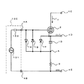
図1は、この参考実施例に係るマイクロホンのインピーダンス変換器を示すブロック図である。これによると、このマイクロホンのインピーダンス変換器は、バイアス回路1、三極管2、負荷抵抗3、入力端子4A,4B、電源端子4C、出力端子4Dおよびグランド端子4Eを備え、バイアス回路1は、ダイオード1A,1B、バイアス抵抗1Cおよびコンデンサ1Dを備える。なお、図1では、三極管2のカソードを加熱するヒータ回路の図示を省略している。
【0025】
これらの構成要素の中で、負荷抵抗3および端子4A〜4Eは、図10の負荷抵抗130および端子141〜145と同一であるので、これらの説明を省略する。
【0026】
三極管2は、図10の三極管120と同じように、カソードフォロワで用いられる。ただし、三極管2は、高い相互コンダクタンスを持つ真空管である。三極管2の相互コンダクタンスは、例えば、12500[μMHO]程度のものである。また、三極管2の推奨されるグリッド抵抗は、1[MΩ]である。
【0027】
バイアス回路1は、ダイオード1A,1Bによって、三極管2のグリッドにバイアス電圧を与える回路である。バイアス抵抗1Cの一端が三極管2のカソードに接続され、他端が負荷抵抗3に接続されている。この接続によって、三極管2のプレート電流Ipがバイアス抵抗1Cに流れ、バイアス電圧がバイアス抵抗1Cに発生する。
【0028】
コンデンサ1Dは、バイアス抵抗1Cに並列に接続されている。この接続によって、コンデンサ1Dは、バイアス抵抗1Cを流れる音声信号をバイパスする。ダイオード1A,1Bは、シリコンダイオードである。ダイオード1A,1Bとしては、逆電流が小さく、かつ、接合容量が小さいものが最適である。この参考実施例では、逆電流が5[pA]であり、接合容量が1.2[pF]であるものが、ダイオード1A,1Bとして用いられている。
【0029】
ダイオード1Aのアノードが三極管2のグリッドに接続され、カソードが、バイアス抵抗1Cと負荷抵抗3との結合点Aに接続されている。ダイオード1Bは、ダイオード1Aとは逆並列に接続されている。すなわち、ダイオード1Bのカソードがダイオード1Aのアノードに接続され、ダイオード1Bのアノードがダイオード1Aのカソードに接続されている。これらのダイオード1A,1Bは、次のようにして、三極管2にバイアス電圧を与える。すなわち、図2に示すように、結合点Aに発生するバイアス電圧が電圧Vcであるとき、グリッド電圧を電圧Vdとする。
【0030】
仮に、グリッド電圧Vdがバイアス電圧Vcに比べて低くなるように変動すると、図3の太線で示す、ダイオード1Aの静特性の中で、順方向の電圧・電流特性B1によって、ダイオード1Aに電流が流れる。このときのダイオード1Aによる、0.7[V]前後の値の電圧降下Vfが発生するので、グリッド電圧Vdは、バイアス電圧Vcに比べて、電圧降下Vf分だけ低くなる。この結果、バイアス電圧Vcが浅くなるので、三極管2のプレート電流Ipが増加し、バイアス電圧Vcの値が大きくなる。これにより、グリッド電圧Vdの変動分が抑えられる。
【0031】
このような、グリッド電圧Vdの変動を抑える作用によって、ダイオード1Aの電流が減少し、この作用は、電流がダイオード1Aに流れなくなるまで続く。この結果、ダイオード1Aの静特性の中で、円Cで示す部分の拡大図(図4に示す)から明らかなように、ダイオード1Aの電流がゼロ以下、すなわち、ダイオード1Aの電圧降下Vfがゼロになるように、グリッド電圧Vdの変動が収束し、グリッド電圧Vdがバイアス電圧Vcに等しくなる。
【0032】
また逆に、グリッド電圧Vdがバイアス電圧Vcに比べて高くなるように変動すると、ダイオード1Bによって、グリッド電圧Vdの変動が収束し、グリッド電圧Vdがバイアス電圧Vcに等しくなる。
【0033】
こうして、ダイオード1A,1Bによる収束作用によって、電流がダイオード1A,1Bに流れなくなる。また、ダイオード1A,1Bによる収束作用は、瞬時に行なわれる。この結果、ダイオード1A,1Bは、高抵抗と同じように動作する。この後、コンデンサマイクロホン100からの音声電圧が加えられたときも、同じようにして、ダイオード1A,1Bは高抵抗と同じように動作する。
【0034】
次に、この参考実施例の動作について説明する。直流電源Vbが三極管2に入力されると、直流電源Vbが三極管2のプレートに加えられる。動作の開始段階では、三極管2には、プレート電流Ipが流れていないので、バイアス抵抗1Cによるバイアス電圧がゼロである。これによって、三極管2に大きなプレート電流Ipが流れ、大きなバイアス電圧が発生し、バイアス電圧によって、グリッド電圧が三極管2のグリッドに加えられる。
【0035】
しかる後、バイアス電圧が三極管2の電圧・電流特性と、バイアス抵抗1Cおよび負荷抵抗3とで決められると共に、ダイオード1A,1Bによって、グリッド電圧がバイアス電圧に収束される。この収束状態のときに、ダイオード1A,1Bが高抵抗として動作する。
【0036】
この状態のときに、入力端子4A,4Bにコンデンサマイクロホン100からの音声電圧が加えられると、ダイオード1A,1Bが高抵抗の状態を保って、この音声電圧が三極管2のグリッドに加えられる。すなわち、コンデンサマイクロホン100からの音声電圧が高入力インピーダンスで受け取られる。また、三極管2がカソードフォロワであるので、音声電圧は、低インピーダンスで出力される。
【0037】
このようにして、上記参考実施例によれば、バイアス抵抗の代わりに、ダイオード1A,1Bを用いることによって、このバイアス抵抗11で制限されていた入力インピーダンスを、高くすることができる。
【0038】
次に、図5により、本発明の第1実施例について説明する。なお、先に説明した図1のマイクロホンのインピーダンス変換器と同一もしくは同一と見なされる構成要素には、それと同じ参照符号が付けられている。また、図5では、三極管2のカソードを加熱するヒータ回路の図示を省略している。
【0039】
この第1実施例に係るインピーダンス変換器では、図1のバイアス回路1の中で、バイアス抵抗1Cの代わりに、ダイオード1Eを用いる。ダイオード1Eは、シリコンダイオードであり、ダイオード1Eのアノードが三極管2のカソードに接続され、ダイオード1Eのカソードが結合点Aに接続されている。
【0040】
ダイオード1Eは、三極管2用のバイアス電圧を発生する。すなわち、三極管2のプレート電流Ipがダイオード1Eを流れることによって、ダイオード1Eには、電圧降下が発生する。この電圧降下は、先の図3に示すように、バイアス抵抗1Cによる電圧降下に比較して、ほぼ一定の値である。三極管2のグリッドには、ダイオード1Eの電圧降下によるバイアス電圧が加えられる。
【0041】
この結果、三極管2のバラツキによって、プレート電流Ipの値が異なっても、ダイオード1Eによる電圧降下がほぼ一定であるので、三極管2のバラツキの影響を除くことができる。また、ダイオード1Eが三極管2のグリッド電圧をほぼ一定にするので、三極管2のプレート電流Ipを安定化することができる。
【0042】
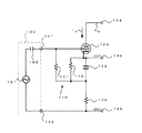
次に、図6により、本発明の第2実施例について説明する。なお、先に説明した図5のマイクロホンのインピーダンス変換器と同一もしくは同一と見なされる構成要素には、それと同じ参照符号が付けられている。また、図6では、三極管2,4のカソードを加熱するヒータ回路の図示を省略している。
【0043】
この第2実施例に係るインピーダンス変換器は、図1,2で用いられている負荷抵抗3の代わりに、定電流負荷を用いる。三極管4と抵抗7との回路は、定電流負荷として動作する。三極管4のプレートが結合点Aに接続され、カソードがグランド端子4Eに接続されている。抵抗7は、三極管4のグリッドとグランド端子4Eとの間に接続されている。
【0044】
この結果、三極管4のグリッドとカソードとが、抵抗7によって常に同電位に保たれるので、三極管4は、一定のプレート電流を流す。これによって、三極管4と抵抗7との回路は、三極管2に対して定電流負荷となる。
【0045】
また、第2実施例では、小さな値の抵抗5が、電源端子4Cと三極管2のプレートとの間に接続されている。さらに、コンデンサ6が、三極管2のプレートと三極管4のグリッドとの間に接続されている。これによって、抵抗5に発生する音声電圧がコンデンサ6を通って三極管4のグリッドに加えられる。この結果、音声電圧の歪みを改善することができる。
【0046】
次に、図7により、本発明の第3実施例について説明する。なお、先に説明した図6のマイクロホンのインピーダンス変換器と同一もしくは同一と見なされる構成要素には、それと同じ参照符号が付けられている。
【0047】
この第3実施例に係るインピーダンス変換器では、ヒータ回路を次のようにしている。すなわち、三極管2のカソードを加熱するヒータ21と、三極管4を加熱するヒータ41とが直列に接続され、ヒータ21,41の直列回路が、加熱用の電圧を入力する端子4Fと、グランド端子4Eとの間に接続されている。また、ヒータ21,41の直列回路には、コンデンサ11が並列に接続されている。
【0048】
コンデンサ11は、電気二重層コンデンサである。電気二重層コンデンサ11は、図8に示すように、電解質13Cをはさむように、活性炭電極13A,13Bを設けた構造をしている。電極として用いられる活性炭電極13A,13Bは、表面積が大きいため、電解コンデンサに比較して大きな静電容量を持つ。
【0049】
一方、ヒータ21,41は、熱が伝わりやすいように、三極管2,4のカソードに接近して設けられている。このために、ヒータ21,41と、三極管2,4のカソードとの間には、静電容量が発生する。この静電容量による静電結合によって、雑音(以下、ヒータ雑音と記す)が音声電圧に加えられて、出力端子4Dから出力される。
【0050】
ヒータ雑音は、ヒータ21,41の動作抵抗と、高温加熱による熱雑音と、一様でない電子放出とに起因する。たとえば、ヒータ21,41が酸化物陰極の場合、ヒータ21,41の動作抵抗が21[Ω]であり、加熱温度が980〜1200[K]である。
【0051】
このようなヒータ雑音を発生するヒータ21,41を、コンデンサ11は、大きな容量によって交流的に短絡する。これによって、コンデンサ11がヒータ雑音を除くことができる。
【0052】
この第3実施例は以下に示す良好な特性を持つ。コンデンサマイクロホン100のコンデンサ102として65[pF]のものを用い、直流電圧Vb(B電源)を120[V]、消費電流8[mA]とし、ヒータ電圧Vh(A電源)を6.3[V]、消費電流0.3[A]とした場合、次のようになる。
最大出力レベル:26[dBV]
(THD 1パーセント、1[kHz])
残留雑音:−112[dBV](A−WEIGHT)
出力インピーダンス:160[Ω]
通過損失:−1[dB]
【0053】
基準出力レベルを−33[dBV]とした場合、第3実施例の特性は、次のようになる。
ヘッドマージン:59[dB]
S/N比:79[dB]
ダイナミックレンジ:138[dB]
【0054】
第3実施例に実際のコンデンサマイクロホンを接続した場合の特性は、次のようになる。
周波数応答:20〜20[kHz]
感度:−33[dB/Pa](1[kHz])
出力インピーダンス:200[Ω]
S/N比:76[dB](A−WEIGHT)
最大許容入力音圧レベル:150[dB]
(THD 1パーセント、1[kHz])
ダイナミックレンジ:132[dB]以上
【0055】
第3実施例の、0度および180度の指向性による周波数応答特性を図9に示す。これによると、応答周波数が低域まで延びている点、通過損失が小さい点から、第3実施例が十分に高い入力インピーダンスと小さい入力容量とを持つことが示される。
【0056】
最後に、第3実施例の性能と、他社であるA社〜F社との性能との比較結果を表1に示す。
【0057】
【表1】

この表1から明らかなように、第3実施例は、他のインピーダンス変換器に比較して、優れたダイナミックレンジを持つ。
【0059】
以上、第1ないし第3実施例について説明したが、本発明は、これに限定されるものではない。例えば、上記実施例では、ダイオード1A,1B,1Eとして、1つのダイオードを用いたが、複数のダイオードを直列に接続したものを、1つのダイオードとして用いてもよい。
【0060】
特に、ダイオード1Eとしては、必要なバイアス電圧が得られるまで、ダイオードを直列に接続したものを用いることができる。同じように、必要に応じて、コンデンサ11に別の電気二重層コンデンサを並列に接続してもよい。
【0061】
【発明の効果】
以上説明したように、本発明によれば、増幅管のグリッドに接続した2つのダイオードによってバイアス電圧を与え、このとき2つのダイオードには、電流が流れない。この結果、大幅な回路変更を不要にして、入力インピーダンスを従来に比べて高くすることができる。
【0062】
また、第3のダイオードに発生する電圧降下をバイアス電圧とするので、バイアス電圧を一定に保つことができる。この結果、従来のカソード抵抗をダイオードに置き換えるだけで、各増幅管の差によってプレート電流がばらついても、バイアス電圧の変化を防ぐことができる。
【0063】
さらに、静電容量の大きな電気二重層コンデンサをヒータに対して、並列に接続するので、ヒータが原因で増幅管のカソードに発生するハム雑音を短絡して、このハム雑音を除くことができる。
【図面の簡単な説明】
【図1】本発明の参考実施例に係るマイクロホンのインピーダンス変換器を示したブロック図。
【図2】上記参考実施例のバイアス回路の動作を説明するための説明図。
【図3】上記参考実施例に用いられるダイオードの特性を示す電圧・電流特性図。
【図4】上記参考実施例に用いられるダイオードの特性の拡大図。
【図5】本発明の第1実施例に係るマイクロホンのインピーダンス変換器を示したブロック図。
【図6】本発明の第2実施例に係るマイクロホンのインピーダンス変換器を示したブロック図。
【図7】本発明の第3実施例に係るマイクロホンのインピーダンス変換器を示したブロック図。
【図8】上記第3実施例に用いられる電気二重層コンデンサを説明するための説明図。
【図9】上記第3実施例の周波数応答を示す特性図。
【図10】従来のインピーダンス変換器を示したブロック図。
【符号の説明】
1 バイアス回路
1A,1B,1E ダイオード
1C バイアス抵抗
1D コンデンサ
2 三極管
3 負荷抵抗
4A,4B 入力端子
4C 電源端子
4D 出力端子
4E グランド端子[0001]
BACKGROUND OF THE INVENTION
The present invention relates to an impedance converter for converting impedance, and more particularly to an impedance converter using a vacuum tube suitable for a condenser microphone.
[0002]
[Prior art]
Some impedance converters receive an input voltage with a high impedance and output with a low impedance. This impedance converter has various uses, for example, is used for a condenser microphone.
[0003]
Since the condenser microphone has a small effective capacitance, it is necessary to receive the voice voltage from the condenser microphone with a high input impedance in order to ensure a frequency response up to a low frequency. Further, since the condenser microphone is connected to the amplifier by a cable or the like, a low output impedance is required when the audio voltage of the condenser microphone is sent to the amplifier. For this purpose, the condenser microphone includes an impedance converter having a high input impedance and a low output impedance.
[0004]
Some impedance converters use a vacuum tube in order to maintain good sound from the condenser microphone. This impedance converter is shown in FIG. The impedance converter includes a bias circuit 110, a
[0005]
The input terminals 141 and 142 are terminals for connecting the
[0006]
A DC power supply Vb for driving the
[0007]
The
[0008]
The bias circuit 110 gives a bias voltage to the
[0009]
The
[0010]
The impedance converter having such a configuration receives the audio voltage generated by the
[0011]
[Problems to be solved by the invention]
However, the technique described above has a problem that the input impedance is limited by the grid resistor 111 of the bias circuit 110. That is, when the
[0012]
For this reason, in order to lower the output impedance, it is necessary to select a vacuum tube having a high transconductance as the
[0013]
On the other hand, if the grid resistance 111 is increased in order to increase the input impedance, the voltage across the grid resistance 111 increases due to the grid leakage current, so that the bias voltage of the vacuum tube changes, which makes the operation of the vacuum tube unstable. become.
[0014]
When the
[0015]
The present invention has been made to solve such a problem, and an object of the present invention is to provide an impedance converter having an input impedance higher than that of the conventional one except for the limitation due to the grid resistance.
[0016]
[Means for Solving the Problems]
In order to achieve the above object, the present invention provides an impedance converter having a plate-grounded amplifier tube and a bias circuit for generating a bias voltage applied to a grid of the amplifier tube, wherein the bias circuit includes the amplifier tube. A first diode for applying the bias voltage to the grid so that a current flows toward the grid, a second diode connected in antiparallel with the first diode, and a load resistor from the cathode of the amplifier tube A third diode connected between the cathode and the load resistor so that a current flows toward the substrate, and a voltage generated in the third diode by a plate current flowing in the amplifier tube is through the first diode and the second diode, characterized in that it added as the bias voltage to the grid of the amplifier tubes It is.
[0017]
In the present invention, it is preferable to connect a capacitor in parallel to the third diode.
[0018]
In an aspect including a heater circuit that applies a voltage to a heater that heats the cathode of the amplifier tube, the heater circuit preferably includes an electric double layer capacitor that short-circuits the heater of the amplifier tube in an AC manner.
[0019]
In the present invention, it is preferable that the input voltage applied to the grid of the amplifier tube is an audio output from a condenser microphone.
[0020]
According to the present invention, a first diode and a second diode are connected in parallel, and a bias voltage is applied to the grid of the amplifier tube via the two diodes. The two diodes serve to converge the grid voltage to the bias voltage. At this time, since no current flows through the two diodes, the two diodes operate as a high resistance. As a result, the input impedance can be increased as compared with the conventional case.
[0021]
Further, the voltage generated in the third diode connected between the cathode and the load resistor is set as a bias voltage applied to the amplifier tube. Since the current flows and the voltage generated in the diode is almost constant, the bias voltage can be kept constant.
[0022]
Furthermore, since the electric double layer capacitor having a large capacitance is connected in parallel to the heater, noise generated at the cathode of the amplifier tube due to the heater can be eliminated.
[0023]
DETAILED DESCRIPTION OF THE INVENTION
Next, in order to better understand the technical concept of the present invention, first with reference to FIGS. 1 to 4, will be described in Reference Examples of the present invention. In this reference embodiment , components that are the same as or the same as those in FIG. 10 described above are given the same reference numerals.
[0024]
FIG. 1 is a block diagram showing an impedance converter of a microphone according to this reference embodiment . According to this, the impedance converter of the microphone includes a
[0025]
Among these components, the
[0026]
The
[0027]
The
[0028]
The capacitor 1D is connected in parallel to the bias resistor 1C. With this connection, the capacitor 1D bypasses the audio signal flowing through the bias resistor 1C. The diodes 1A and 1B are silicon diodes. As the diodes 1A and 1B, those having a small reverse current and a small junction capacitance are optimal. In this reference embodiment , diodes 1A and 1B having a reverse current of 5 [pA] and a junction capacitance of 1.2 [pF] are used.
[0029]
The anode of the
[0030]
If the grid voltage Vd fluctuates so as to be lower than the bias voltage Vc, a current is supplied to the diode 1A due to the forward voltage / current characteristic B1 in the static characteristic of the diode 1A shown by the thick line in FIG. Flowing. At this time, a voltage drop Vf having a value of about 0.7 [V] is generated by the diode 1A. Therefore, the grid voltage Vd is lower than the bias voltage Vc by the voltage drop Vf. As a result, since the bias voltage Vc becomes shallow, the plate current Ip of the
[0031]
By such an action of suppressing the fluctuation of the grid voltage Vd, the current of the diode 1A is reduced, and this action continues until no current flows to the diode 1A. As a result, as apparent from the enlarged view (shown in FIG. 4) of the portion indicated by the circle C in the static characteristics of the diode 1A, the current of the diode 1A is less than zero, that is, the voltage drop Vf of the diode 1A is zero. So that the fluctuation of the grid voltage Vd converges, and the grid voltage Vd becomes equal to the bias voltage Vc.
[0032]
Conversely, when the grid voltage Vd fluctuates so as to be higher than the bias voltage Vc, the fluctuation of the grid voltage Vd is converged by the diode 1B, and the grid voltage Vd becomes equal to the bias voltage Vc.
[0033]
Thus, no current flows through the diodes 1A and 1B due to the convergence effect of the diodes 1A and 1B. Further, the convergence effect by the diodes 1A and 1B is instantaneously performed. As a result, the diodes 1A and 1B operate in the same manner as the high resistance. Thereafter, when the audio voltage from the
[0034]
Next, the operation of this reference embodiment will be described. When the DC power supply Vb is input to the
[0035]
Thereafter, the bias voltage is determined by the voltage / current characteristics of the
[0036]
In this state, when the audio voltage from the
[0037]
Thus, according to the reference embodiment, the input impedance limited by the bias resistor 11 can be increased by using the diodes 1A and 1B instead of the bias resistor.
[0038]
Next, the first embodiment of the present invention will be described with reference to FIG. Note that the same reference numerals are assigned to components that are considered to be the same as or the same as the impedance converter of the microphone of FIG. 1 described above. Further, in FIG. 5, illustration of a heater circuit for heating the cathode of the
[0039]
In the impedance converter according to the first embodiment , a
[0040]
The
[0041]
As a result, the voltage drop due to the
[0042]
Next, a second embodiment of the present invention will be described with reference to FIG. Note that the same reference numerals are assigned to components that are considered to be the same as or the same as the impedance converter of the microphone of FIG. 5 described above. Further, in FIG. 6, illustration of a heater circuit for heating the cathodes of the
[0043]
The impedance converter according to the second embodiment uses a constant current load instead of the
[0044]
As a result, since the grid and the cathode of the
[0045]
In the second embodiment , a resistor 5 having a small value is connected between the
[0046]
Next, a third embodiment of the present invention will be described with reference to FIG. Note that the same reference numerals are assigned to components that are considered to be the same as or the same as the impedance converter of the microphone of FIG. 6 described above.
[0047]
In the impedance converter according to the third embodiment , the heater circuit is as follows. That is, a
[0048]
The capacitor 11 is an electric double layer capacitor. As shown in FIG. 8, the electric double layer capacitor 11 has a structure in which activated carbon electrodes 13A and 13B are provided so as to sandwich an electrolyte 13C. Since the activated carbon electrodes 13A and 13B used as electrodes have a large surface area, they have a large capacitance compared to the electrolytic capacitor.
[0049]
On the other hand, the
[0050]
The heater noise is caused by operating resistance of the
[0051]
The capacitor 11 short-circuits the
[0052]
This third embodiment has the following good characteristics. The
Maximum output level: 26 [dBV]
(
Residual noise: -112 [dBV] (A-WEIGHT)
Output impedance: 160 [Ω]
Passage loss: -1 [dB]
[0053]
When the reference output level is −33 [dBV], the characteristics of the third embodiment are as follows.
Head margin: 59 [dB]
S / N ratio: 79 [dB]
Dynamic range: 138 [dB]
[0054]
The characteristics when an actual condenser microphone is connected to the third embodiment are as follows.
Frequency response: 20-20 [kHz]
Sensitivity: -33 [dB / Pa] (1 [kHz])
Output impedance: 200 [Ω]
S / N ratio: 76 [dB] (A-WEIGHT)
Maximum allowable input sound pressure level: 150 [dB]
(
Dynamic range: 132 [dB] or more
FIG. 9 shows frequency response characteristics according to directivity of 0 degrees and 180 degrees in the third embodiment . According to this, it is shown that the third embodiment has a sufficiently high input impedance and a small input capacitance from the point that the response frequency extends to a low band and the point that the passage loss is small.
[0056]
Finally, Table 1 shows a comparison result between the performance of the third example and the performances of other companies, Company A to Company F.
[0057]
[Table 1]
As is apparent from Table 1, the third embodiment has an excellent dynamic range as compared with other impedance converters.
[0059]
Has been described with the first to third embodiments, the present invention is not limited thereto. For example, in the above embodiment, one diode is used as the
[0060]
In particular, as the
[0061]
【The invention's effect】
As described above, according to the present invention, the bias voltage is applied by the two diodes connected to the grid of the amplifier tube, and at this time, no current flows through the two diodes. As a result, it is possible to make the input impedance higher than in the prior art without requiring a significant circuit change.
[0062]
In addition, since the voltage drop generated in the third diode is used as the bias voltage, the bias voltage can be kept constant. As a result, by simply replacing the conventional cathode resistance with a diode, a change in bias voltage can be prevented even if the plate current varies due to the difference between the amplifier tubes.
[0063]
Furthermore, since the electric double layer capacitor having a large capacitance is connected in parallel to the heater, the hum noise generated at the cathode of the amplifier tube due to the heater can be short-circuited to eliminate this hum noise.
[Brief description of the drawings]
FIG. 1 is a block diagram showing a microphone impedance converter according to a reference embodiment of the present invention.
FIG. 2 is an explanatory diagram for explaining the operation of the bias circuit of the reference embodiment.
FIG. 3 is a voltage / current characteristic diagram showing characteristics of a diode used in the reference embodiment.
FIG. 4 is an enlarged view of characteristics of a diode used in the reference embodiment.
FIG. 5 is a block diagram showing a microphone impedance converter according to the first embodiment of the present invention;
FIG. 6 is a block diagram showing an impedance converter of a microphone according to a second embodiment of the present invention.
FIG. 7 is a block diagram showing an impedance converter of a microphone according to a third embodiment of the present invention.
FIG. 8 is an explanatory diagram for explaining an electric double layer capacitor used in the third embodiment.
FIG. 9 is a characteristic diagram showing a frequency response of the third embodiment.
FIG. 10 is a block diagram showing a conventional impedance converter.
[Explanation of symbols]
DESCRIPTION OF
Claims (4)
上記バイアス回路は、上記増幅管のグリッドに向けて電流を流すように上記バイアス電圧を上記グリッドに加える第1のダイオードと、上記第1のダイオードと逆並列に接続された第2のダイオードと、上記増幅管のカソードから負荷抵抗に向けて電流を流すように上記カソードと上記負荷抵抗との間に接続された第3のダイオードとを備え、上記増幅管に流れるプレート電流によって上記第3のダイオードに発生する電圧を、上記第1のダイオードおよび上記第2のダイオードを介して上記増幅管のグリッドに上記バイアス電圧として加えることを特徴とするインピーダンス変換器。In an impedance converter having a plate-grounded amplifier tube and a bias circuit for generating a bias voltage applied to the grid of the amplifier tube,
The bias circuit includes: a first diode that applies the bias voltage to the grid so that a current flows toward the grid of the amplifier tube; and a second diode that is connected in antiparallel with the first diode; A third diode connected between the cathode and the load resistor so that a current flows from the cathode of the amplifier tube toward the load resistor, and the third diode is generated by a plate current flowing through the amplifier tube. The impedance converter is characterized in that the voltage generated in is applied as the bias voltage to the grid of the amplifier tube via the first diode and the second diode.
Priority Applications (2)
| Application Number | Priority Date | Filing Date | Title |
|---|---|---|---|
| JP12439998A JP4227679B2 (en) | 1998-05-07 | 1998-05-07 | Impedance converter |
| US09/299,851 US6453048B1 (en) | 1998-05-07 | 1999-04-26 | Impedance converter for a condenser microphone |
Applications Claiming Priority (1)
| Application Number | Priority Date | Filing Date | Title |
|---|---|---|---|
| JP12439998A JP4227679B2 (en) | 1998-05-07 | 1998-05-07 | Impedance converter |
Publications (2)
| Publication Number | Publication Date |
|---|---|
| JPH11317996A JPH11317996A (en) | 1999-11-16 |
| JP4227679B2 true JP4227679B2 (en) | 2009-02-18 |
Family
ID=14884486
Family Applications (1)
| Application Number | Title | Priority Date | Filing Date |
|---|---|---|---|
| JP12439998A Expired - Fee Related JP4227679B2 (en) | 1998-05-07 | 1998-05-07 | Impedance converter |
Country Status (2)
| Country | Link |
|---|---|
| US (1) | US6453048B1 (en) |
| JP (1) | JP4227679B2 (en) |
Cited By (2)
| Publication number | Priority date | Publication date | Assignee | Title |
|---|---|---|---|---|
| US9736586B2 (en) | 2015-12-21 | 2017-08-15 | Kabushiki Kaisha Audio-Technica | Condenser microphone |
| US9893691B2 (en) | 2015-12-25 | 2018-02-13 | Kabushiki Kaisha Audio-Technica | Impedance converter and condenser microphone |
Families Citing this family (22)
| Publication number | Priority date | Publication date | Assignee | Title |
|---|---|---|---|---|
| JP4057212B2 (en) * | 2000-02-15 | 2008-03-05 | 三菱電機株式会社 | Microphone device |
| FI109641B (en) * | 2000-03-10 | 2002-09-13 | Nokia Corp | microphone structure |
| WO2002073792A2 (en) * | 2001-03-09 | 2002-09-19 | Techtronic A/S | An electret condensor microphone preamplifier that is insensitive to leakage currents at the input |
| JP3890301B2 (en) * | 2003-01-15 | 2007-03-07 | 株式会社オーディオテクニカ | Condenser microphone |
| JP4426902B2 (en) * | 2004-05-14 | 2010-03-03 | 株式会社オーディオテクニカ | Condenser microphone |
| JP4440121B2 (en) | 2005-01-06 | 2010-03-24 | Necエレクトロニクス株式会社 | Voltage supply circuit and microphone unit |
| US7929716B2 (en) | 2005-01-06 | 2011-04-19 | Renesas Electronics Corporation | Voltage supply circuit, power supply circuit, microphone unit using the same, and microphone unit sensitivity adjustment method |
| JP2006245740A (en) * | 2005-03-01 | 2006-09-14 | Sanyo Electric Co Ltd | Amplifier circuit and electret condenser microphone using same |
| US20070229123A1 (en) * | 2006-03-30 | 2007-10-04 | Chien-Chin Hsiao | Semiconductor device for microphone applications |
| JP4764234B2 (en) * | 2006-04-07 | 2011-08-31 | 株式会社東芝 | Impedance conversion circuit and electronic device |
| JP2008147806A (en) * | 2006-12-07 | 2008-06-26 | Audio Technica Corp | Condenser microphone and manufacturing method therefor |
| JP5081245B2 (en) * | 2007-08-22 | 2012-11-28 | パナソニック株式会社 | Directional microphone device |
| US8401208B2 (en) * | 2007-11-14 | 2013-03-19 | Infineon Technologies Ag | Anti-shock methods for processing capacitive sensor signals |
| JP5060980B2 (en) * | 2008-01-31 | 2012-10-31 | 株式会社オーディオテクニカ | Condenser microphone unit and its fixed pole |
| JP2009225100A (en) * | 2008-03-17 | 2009-10-01 | Nec Electronics Corp | Semiconductor integrated circuit and capacitor microphone |
| JP5201594B2 (en) * | 2009-04-24 | 2013-06-05 | 株式会社オーディオテクニカ | Condenser microphone and its impedance converter |
| JP5201596B2 (en) * | 2009-05-22 | 2013-06-05 | 株式会社オーディオテクニカ | Microphone impedance converter and microphone |
| US8253471B2 (en) * | 2009-10-09 | 2012-08-28 | Fairchild Semiconductor Corporation | High impedance bias network |
| JP5631256B2 (en) * | 2011-04-25 | 2014-11-26 | 株式会社オーディオテクニカ | Condenser microphone unit and condenser microphone |
| JP5967823B2 (en) * | 2012-10-24 | 2016-08-10 | 株式会社オーディオテクニカ | Variable directivity condenser microphone |
| JP6667379B2 (en) * | 2016-06-16 | 2020-03-18 | 株式会社オーディオテクニカ | Microphone power supply |
| CN110690282B (en) * | 2019-08-23 | 2022-10-18 | 福建省福联集成电路有限公司 | Transistor-based resistor structure and manufacturing method thereof |
Family Cites Families (9)
| Publication number | Priority date | Publication date | Assignee | Title |
|---|---|---|---|---|
| JPS57193198A (en) * | 1981-05-22 | 1982-11-27 | Toshiba Corp | Electrostatic microphone |
| US4629910A (en) * | 1982-04-21 | 1986-12-16 | At&T Bell Laboratories | High input impedance circuit |
| SE452083C (en) * | 1983-02-25 | 1990-11-15 | Rune Rosander | MICROPHONE |
| IT1239899B (en) * | 1990-03-22 | 1993-11-23 | Sgs Thomson Microelectronics | LOW NOISE AND HIGH INPUT IMPEDANCE AMPLIFIER, PARTICULARLY FOR MICROPHONES |
| JP2734265B2 (en) * | 1991-12-12 | 1998-03-30 | 日本電気株式会社 | Amplifier circuit for electret condenser microphone |
| JP3437237B2 (en) * | 1994-01-21 | 2003-08-18 | 松下電器産業株式会社 | Amplifier |
| US5446413A (en) * | 1994-05-20 | 1995-08-29 | Knowles Electronics, Inc. | Impedance circuit for a miniature hearing aid |
| SE506362C2 (en) * | 1996-04-22 | 1997-12-08 | Bilsom Ab | microphone circuit |
| US6160450A (en) * | 1999-04-09 | 2000-12-12 | National Semiconductor Corporation | Self-biased, phantom-powered and feedback-stabilized amplifier for electret microphone |
-
1998
- 1998-05-07 JP JP12439998A patent/JP4227679B2/en not_active Expired - Fee Related
-
1999
- 1999-04-26 US US09/299,851 patent/US6453048B1/en not_active Expired - Lifetime
Cited By (2)
| Publication number | Priority date | Publication date | Assignee | Title |
|---|---|---|---|---|
| US9736586B2 (en) | 2015-12-21 | 2017-08-15 | Kabushiki Kaisha Audio-Technica | Condenser microphone |
| US9893691B2 (en) | 2015-12-25 | 2018-02-13 | Kabushiki Kaisha Audio-Technica | Impedance converter and condenser microphone |
Also Published As
| Publication number | Publication date |
|---|---|
| US6453048B1 (en) | 2002-09-17 |
| JPH11317996A (en) | 1999-11-16 |
Similar Documents
| Publication | Publication Date | Title |
|---|---|---|
| JP4227679B2 (en) | Impedance converter | |
| US5128566A (en) | Variable attenuator circuit | |
| JP3263089B2 (en) | Low voltage analog front end | |
| CN108429541A (en) | Predistorter for compensating for linearity of amplifier | |
| JPH11340785A (en) | Active low-pass filter | |
| US7262666B2 (en) | Amplifier circuit having an extended Wilson current-mirror self-bias boosting circuit | |
| US5352992A (en) | Amplifier circuit | |
| EP0828344A2 (en) | Integrated circuit and method for generating a transimpedance function | |
| JP3404209B2 (en) | Transimpedance amplifier circuit | |
| JP2004527169A (en) | Amplifier circuit | |
| JP2016103765A (en) | Impedance conversion circuit for capacitor microphone | |
| JPH08316759A (en) | Broad band amplifier | |
| JP4083551B2 (en) | Preamplifier | |
| JP4208065B2 (en) | Vacuum tube circuit | |
| JP2000516792A (en) | Amplifiers suitable for cable network applications | |
| KR101665586B1 (en) | Amplifier circuit using vacuum tube | |
| CN216904827U (en) | Current-controlled audio amplifier | |
| JPS6125244B2 (en) | ||
| JPH0418482B2 (en) | ||
| Hilbourne et al. | Transistor power amplifiers | |
| JP3255073B2 (en) | AGC circuit | |
| CN209462348U (en) | Electronic tube power amplifier | |
| JP3332724B2 (en) | Differential amplifier | |
| JP5201594B2 (en) | Condenser microphone and its impedance converter | |
| JP3569902B2 (en) | OTL (OutputTransformerLess) vacuum tube power amplifier |
Legal Events
| Date | Code | Title | Description |
|---|---|---|---|
| A521 | Written amendment |
Free format text: JAPANESE INTERMEDIATE CODE: A523 Effective date: 20050425 |
|
| A621 | Written request for application examination |
Free format text: JAPANESE INTERMEDIATE CODE: A621 Effective date: 20050425 |
|
| A131 | Notification of reasons for refusal |
Free format text: JAPANESE INTERMEDIATE CODE: A131 Effective date: 20080109 |
|
| A521 | Written amendment |
Free format text: JAPANESE INTERMEDIATE CODE: A523 Effective date: 20080305 |
|
| A131 | Notification of reasons for refusal |
Free format text: JAPANESE INTERMEDIATE CODE: A131 Effective date: 20080507 |
|
| A521 | Written amendment |
Free format text: JAPANESE INTERMEDIATE CODE: A523 Effective date: 20080701 |
|
| TRDD | Decision of grant or rejection written | ||
| A01 | Written decision to grant a patent or to grant a registration (utility model) |
Free format text: JAPANESE INTERMEDIATE CODE: A01 Effective date: 20081105 |
|
| A01 | Written decision to grant a patent or to grant a registration (utility model) |
Free format text: JAPANESE INTERMEDIATE CODE: A01 |
|
| A61 | First payment of annual fees (during grant procedure) |
Free format text: JAPANESE INTERMEDIATE CODE: A61 Effective date: 20081201 |
|
| FPAY | Renewal fee payment (event date is renewal date of database) |
Free format text: PAYMENT UNTIL: 20111205 Year of fee payment: 3 |
|
| R150 | Certificate of patent or registration of utility model |
Free format text: JAPANESE INTERMEDIATE CODE: R150 |
|
| FPAY | Renewal fee payment (event date is renewal date of database) |
Free format text: PAYMENT UNTIL: 20121205 Year of fee payment: 4 |
|
| FPAY | Renewal fee payment (event date is renewal date of database) |
Free format text: PAYMENT UNTIL: 20141205 Year of fee payment: 6 |
|
| R250 | Receipt of annual fees |
Free format text: JAPANESE INTERMEDIATE CODE: R250 |
|
| R250 | Receipt of annual fees |
Free format text: JAPANESE INTERMEDIATE CODE: R250 |
|
| R250 | Receipt of annual fees |
Free format text: JAPANESE INTERMEDIATE CODE: R250 |
|
| LAPS | Cancellation because of no payment of annual fees |