JP4227291B2 - Scanning optical device and image forming apparatus using the same - Google Patents
Scanning optical device and image forming apparatus using the same Download PDFInfo
- Publication number
- JP4227291B2 JP4227291B2 JP2000181482A JP2000181482A JP4227291B2 JP 4227291 B2 JP4227291 B2 JP 4227291B2 JP 2000181482 A JP2000181482 A JP 2000181482A JP 2000181482 A JP2000181482 A JP 2000181482A JP 4227291 B2 JP4227291 B2 JP 4227291B2
- Authority
- JP
- Japan
- Prior art keywords
- diffraction
- optical element
- diffraction order
- light beam
- scanning
- Prior art date
- Legal status (The legal status is an assumption and is not a legal conclusion. Google has not performed a legal analysis and makes no representation as to the accuracy of the status listed.)
- Expired - Fee Related
Links
Images


Description
【0001】
【発明の属する技術分野】
本発明は回折光学素子を用いた走査光学装置に関し、特に光源手段から出射した光束を偏向素子で偏向させfθ特性を有する結像素子を介して被走査面上を光走査して画像情報を記録するようにした、例えば電子写真プロセスを有するレーザービームプリンターやデジタル複写機等の装置に好適なものである。
【0002】
【従来の技術】
従来よりレーザービームプリンター(LBP)やデジタル複写機等の走査光学装置においては画像信号に応じて光源手段から光変調され出射した光束を、例えば回転多面鏡(ポリゴンミラー)より成る光偏向器により周期的に偏向させ、fθ特性を有する結像光学系によって感光性の記録媒体(感光ドラム)面上にスポット状に集束させ、その面上を光走査して画像記録を行っている。
【0003】
図9は従来の走査光学装置の要部概略図である。
【0004】
同図において光源手段91から出射した発散光束はコリメーターレンズ92により略平行光束とされ、絞り93によって該光束を制限して副走査方向にのみ所定の屈折力を有するシリンドリカルレンズ(シリンダーレンズ)94に入射する。シリンドリカルレンズ94に入射した略平行光束のうち主走査面内においてはそのまま略平行光束の状態で射出する。また副走査面内においては集束して回転多面鏡(ポリゴンミラー)から成る光偏向器95の偏向面(反射面)95aにほぼ線像として結像している。
【0005】
そして光偏向器95の偏向面95aで偏向反射された光束をfθ特性を有する走査光学系(fθレンズ)96を介して被走査面としての感光ドラム面98上に導光し、該光偏向器95を矢印A方向に回転させることによって、該感光ドラム面98上を矢印B方向(主走査方向)に光走査して画像情報の記録を行なっている。
【0006】
【発明が解決しようとする課題】
上記の走査光学装置では非球面を用いて高精度な収差補正が可能なこと、また射出成形による低コスト化が行なえることから走査光学系としてプラスチック樹脂製のレンズを用いた例が数多く提案されている。
【0007】
しかしながらプラスチックレンズは環境変動による収差変動(特にピントずれや倍率ずれ)が大きく、走査光学装置のスポット径を小さくした場合に問題となる。
【0008】
そこで最近ではこのプラスチックレンズ固有の収差変動を補償するために、例えば特開平10-68903 号公報に提案されているように走査光学系として回折光学素子を導入している例もある。同公報では例えば環境温度が上昇した場合、プラスチックレンズの屈折率低下による収差変化を光源である半導体レーザーの波長変動による収差変化で補償されるよう予め回折光学素子を用い色収差を発生させている。
【0009】
また回折光学素子はそれ単独で用いた場合、素子の肉厚が一定となり射出成形で製造する場合、成形性に優れているという特徴をもつ。
【0010】
このように回折光学素子は走査光学装置の光学系として非常に有用なものであるが、その反面、屈折光学素子と異なり回折光学素子では光の利用効率(以下「回折効率η」と呼ぶ、η=設計次数出射光量/入射光量)が様々な条件により異なるという問題点がある。以下に回折格子モデルを使用し説明する。
【0011】
図10は回折光学素子の回折格子モデルの説明図である。同図における回折光学素子は、その格子ピッチp(μm)、格子深さh(μm)の連続格子より成る。尚、格子ピッチpと格子深さhとの比をアスペクト比ARと呼び、AR=格子ピッチp/格子深さhと定義する。
【0012】
ここで回折格子モデルの基盤に対し入射角θiで入射した光束は回折され、設計回折次数方向へ回折される。しかしながら特に格子ピッチpが小さくなってくると理論上回折効率が悪化し、被走査面上における設計回折次数の光量が低下し、設計回折次数以外の回折光(以下「付加回折光」と称す。)も目立ちはじめフレアーやゴースト等の原因となる。
【0013】
図11は図10に示した回折格子モデルにおいて格子部(回折格子)への入射角をθi=0としたときの回折効率のアスペクト比依存性を示す説明図である。同図では格子深さhを一定とし、格子ピッチpを変えることによりアスペクト比ARを振っているが、アスペクト比が4より小さくなると急激に回折効率が悪くなることが分かる。
【0014】
図12は図10に示した回折格子モデルにおいてアスペクト比=3.4(ピッチp=10.2μm、深さh=3.0μm)、格子部への入射角をθi=23°としたときの使用回折次数光、及び付加回折次数における回折効率を示した説明図である。尚、回折効率計算は厳密結合波解析法で算出している。
【0015】
従来では回折格子は使用回折次数の回折効率を向上させることのみから格子形状が決定されていたため、付加回折光は考慮されず特に使用(設計)回折次数に対して+側の回折次数の付加回折光は、
(1)使用回折次数に対して走査速度が遅いため相対的に露光量が多くなる。
(2)使用回折次数に対して回折方向が内側(走査光学系の光軸寄り)となり、必ず被走査面の画像有効域内に入る。逆に−側の回折次数の回折光は付加回折光の多い最軸外光束の通過位置付近において画像有効域外に出る。
【0016】
という問題点があり、−側回折次数の付加回折光と比較しフレアーやゴースト等への影響が大きく、高精細な画像形成を行う上で問題点が大きい。
【0017】
図13は上述の条件下で回折格子のブレーズ角による付加回折光の露光量比(使用回折次数の露光量に対して)の変化を示す説明図である。
【0018】
同図より使用回折次数の回折効率がピークになるブレーズ角より角度を小さくすれば使用回折次数に対して−側回折次数の角度を大きく設定すれば+側回折次数の付加回折光の露光量が増加し、両者が等しくなるブレーズ角近傍で使用回折光が最大となる。従ってブレーズ角を適当に設定することによって使用回折効率を向上させ、+側、−側の付加回折光による影響を均等、かつ最少にすることが可能となる。
【0019】
本発明は回折格子のブレーズ角を適当に設定するという容易な構成で、かつ簡易な方法で回折光学素子固有の付加回折光によるフレアーやゴースト等の影響を低減し、特にその最軸外における回折効率の低下を低減し、被走査面上における像面照度の均一性を高め、諸変動による収差変化が少なく高精細印字に適した回折光学素子を用いた走査光学装置の提供を目的とする。
【0020】
【課題を解決するための手段】
請求項1の発明の走査光学装置は、光源手段と、前記光源手段から出射した光束を偏向する光偏向器と、前記光偏向器の偏向面にて偏向された光束を被走査面上に結像させる走査光学素子と、を有する走査光学装置であって、
前記走査光学素子は、少なくとも1つの回折光学素子を有し、前記回折光学素子で回折された光束のうち、使用回折次数の回折光束を用いて前記被走査面上にスポットを形成しており、
前記回折光学素子は、前記光偏向器の偏向面にて偏向された最軸外光束に対して、前記使用回折次数以外の回折光束のうち、前記使用回折次数より+側の回折次数の回折光束の光量の総和が前記使用回折次数より−側の回折次数の回折光束の光量の総和よりも小さくなるように形成されていることを特徴としている。
【0033】
【発明の実施の形態】
[実施形態1]
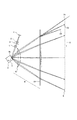
図1は本発明の実施形態1の走査光学装置の要部概略図、図2は本発明の実施形態1の走査光学装置の主走査方向の要部断面図(主走査断面図)である。尚、図2において回折光学素子の格子部(回折格子)は誇張して表現しており、実際の形状とは異なる。
【0034】
図中、1は光源手段であり、例えば半導体レーザーより成っている。2は第1の光学素子としてのコリメーターレンズであり、光源手段1から出射された発散光束を略平行光束に変換している。3は開口絞りであり、通過光束(光量)を制限している。4はシリンドリカルレンズであり、副走査方向にのみ所定の屈折力を有しており、開口絞り3を通過した光束を副走査断面内で後述する光偏向器の偏向面(反射面)にほぼ線像として結像させている。
【0035】
5は偏向素子としての例えばポリゴンミラー(回転多面鏡)より成る光偏向器であり、モーター等の駆動手段(不図示)により図中矢印A方向に一定速度で回転している。
【0036】
6は第2の光学素子としてのfθ特性を有する走査光学素子であり、屈折光学素子61と回折光学素子62とを有している。屈折光学素子61は主走査方向と副走査方向とで互いに異なるパワーを有する単一のプラスチック製のトーリックレンズより成っている。回折光学素子62は主走査方向と副走査方向とで互いに異なるパワーを有するプラスチック製の長尺の回折素子より成っている。
【0037】
本実施形態における回折光学素子62は光偏向器5で偏向された光束のうち、被走査面8の両端部に対応する最軸外光束が該回折光学素子62を通過する位置において、該回折光学素子62で回折される回折次数の回折光のうち、該被走査面8上にスポットを形成させるために使用する使用回折次数の回折光(本実施形態では+2次回折光)に対し、+側回折次数の付加回折光(使用する回折次数以外の回折光)の光量の総和が、−側回折次数の付加回折光の光量の総和よりも小さくなるよう回折格子形状を設定している。この回折格子形状はブレーズ形状より成っている。
【0038】
回折光学素子62以降、図2中の実線72は使用(設計)回折次数である+2次光束、破線71,73は各々順に付加回折光である+1次光束、+3次光束である。尚、付加回折光71,73は最軸外光束のみ図示、+1、+3次以外の付加回折光は不図示である。
【0039】
この回折光学素子62は射出成形により製作されたプラスチック製であるが、ガラス基盤の上にレプリカで回折格子を製作しても同等の効果が得られる。本実施形態では光偏向器5の回転軸と被走査面8の中点から該光偏向器5側にトーリックレンズ61、該被走査面8側に回折光学素子62を配している。これらの光学素子は共に上述の如く主走査方向と副走査方向とに異なるパワーを有しており、光偏向器5からの偏向光束を被走査面8に結像させると共に光偏向器5の偏向面5aの倒れを補正している。
【0040】
8は被走査面である感光ドラム面である。
【0041】
本実施形態において画像情報に応じて半導体レーザー1から光変調され出射した発散光束はコリメーターレンズ2によって略平行光束に変換され、開口絞り3によって該光束(光量)を制限してシリンドリカルレンズ4に入射する。シリンドリカルレンズ4に入射した略平行光束のうち主走査断面内においてはそのままの状態で射出する。また副走査断面内においては収束して光偏向器5の偏向面5aにほぼ線像(主走査方向に長手の線像)として結像している。そして光偏向器5の偏向面5aで偏向された光束はトーリックレンズ61と回折光学素子62とを介して感光ドラム面8上にスポット状に結像され、該光偏向器5を矢印A方向に回転させることによって、該感光ドラム面8上を矢印B方向(主走査方向)に等速度で光走査している。これにより記録媒体である感光ドラム面8上に画像記録を行なっている。
【0042】
本実施形態における走査光学素子6を構成するトーリックレンズ61と回折光学素子62の形状はそれぞれ、
▲1▼トーリックレンズ..主走査方向が10次までの関数で表せる非球面形状、
トーリックレンズと光軸との交点を原点とし、光軸方向をx軸、主走査面内において光軸と直交する軸をy軸、副走査面内において光軸と直交する軸をz軸としたとき、
主走査方向と対応する母線方向が、
【0043】
【外1】

【0044】
副走査方向(光軸を含み主走査方向に対して直交する方向)と対応する子線方向が、
【0045】
【外2】
(但し、r0 は光軸上の子線曲率半径、D2 、D4 、D6 、D8 、D10は係数)
▲2▼回折光学素子..主走査方向が6次まで、副走査方向が主走査方向の位置により異なる2次の位相関数で表される回折面
φ=mλ=b2Y2 +b4Y4 +b6Y6 +(d0 +d1Y1 +d2Y2 +d3Y3 +d4Y4)Z2
(但し、mは回折次数:実施形態1〜3では+2次回折光を使用)
【0046】
表-1に本実施形態における光学配置とトーリックレンズの非球面係数及び回折光学素子の位相項を示す。本実施形態における回折光学素子の格子部の材質の屈折率はn=1.51742、波長はλ=780(nm)、最軸外光束において回折格子に入射する光束の入射角はθi=23°、格子ピッチはp=10.2(μm)である。
【0047】
【表1】
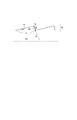
図3は本実施形態における回折光学素子の主走査方向の要部断面図であり、格子部を拡大して示したものである。同図では単一格子のみを図示してある。
【0049】
同図において回折格子21は主にパワーを発生させる傾斜部31、傾斜部31の端部と基盤部22とをつなぐ壁部32とより構成されており、基盤部22と傾斜部31はブレーズ角θを成し、傾斜部31と壁部32は常に直角を成している。
【0050】
本実施形態では前述の如く光偏向器5で偏向された光束のうち、被走査面8の両端部に対応する最軸外光束が回折光学素子62を通過する位置において、該回折光学素子62で回折される回折次数の回折光のうち、該被走査面8上にスポットを形成させるために使用する使用回折次数の回折光(+2次回折光)に対し、+側回折次数の付加回折光の光量の総和が、−側回折次数の付加回折光の光量の総和よりも小さくなるよう回折格子形状を設定している。ここで最軸外光束が回折光学素子62を通過する位置における回折格子のブレーズ角θは、
θ=sin-1(mλ/p(n-1))
但し、
m:使用回折次数
λ:波長
p:格子ピッチ
n:格子部の材質の屈折率
の関係を満たすよう設定されており、最軸外光束の通過位置では、
θ=17.811°と成っている。
【0051】
尚、上記の最軸外光束が回折光学素子62を通過する位置における回折格子のブレーズ角θを、
θ=tan-1(mλ/p(n-1))
の関係を満たすよう設定しても良い。
【0052】
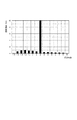
図4は本実施形態における使用回折次数、及び付加回折次数における回折効率を示した説明図である。尚、回折効率計算は厳密結合波解析法で算出している。
【0053】
同図に示すように本実施形態における回折格子では使用回折次数に対し+側回折次数の付加回折光の光量の総和が、−側回折次数の付加回折光の光量の総和よりも小さく設定されていることがわかる。
【0054】
このように本実施形態では相対的に走査速度が遅いため露光量が大きく、かつ画像有効域内に回折するため目立ちやすい+側回折次数の回折光束を低減するという効果を有する。
【0055】
本実施形態では上述の如く回折光学素子の回折格子のブレーズ角を適当に設定するという容易な方法により、使用回折次数の回折効率を低下させることなく、回折光学素子を走査光学装置で使用する上で問題となる+側回折次数の回折光束によるフレアーやゴースト等を低減し、高精細印字に適した走査光学装置を実現することが可能となる。
【0056】
[実施形態2]
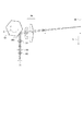
図5は本発明の実施形態2の回折光学素子の主走査方向の要部断面図であり、格子部を拡大して示したものである。同図において図3に示した要素と同一要素には同符番を付している。同図では単一格子のみを図示してある。
【0057】
本実施形態において前述の実施形態1と異なる点は回折格子のブレーズ角θの設定方法を実施形態1と異ならせた点、即ち被走査面の両端部だけでなく該被走査面全域において使用回折次数に対し+側回折次数の光量の総和を−側回折次数の光量の総和に対して小さくした点であり、その他の走査光学素子の設定パラメーターや格子ピッチ等は実施形態1と略同様であり、これにより同様な効果を得ている。
【0058】
即ち、本実施形態においては回折光学素子の回折格子のブレーズ角θを、
θ=tan-1(mλ/p(n-1))
の関係を満たすよう設定しており、入射光束の通過位置では、
θ=17.008°
と成っている。
【0059】
尚、上記回折光学素子の回折格子のブレーズ角θを、
θ=sin-1(mλ/p(n-1))
の関係を満たすよう設定しても良い。
【0060】
図6は本実施形態における使用回折次数、及び付加回折次数における回折効率を示した説明図である。尚、回折効率計算は厳密結合波解析法で算出している。
【0061】
同図に示すように本実施形態における回折格子では使用回折次数に対し+側回折次数の付加回折光の光量の総和が、−側回折次数の付加回折光の光量の総和よりも小さく設定されていることがわかる。
【0062】
図7は各像高における隣接回折次数(本実施形態ではm=+1、+3次)での回折効率を示す説明図である。同図は隣接回折次数のみの図示であるが、全像高において+側回折次数である+3次光束の回折効率の方が−側回折次数である+1次光束の回折効率より小さく設定されている。
【0063】
このように本実施形態では相対的に走査速度が遅いため露光量が大きく、かつ画像有効域内に回折するため目立ちやすい+側回折次数の回折光束を低減するという効果を有する。
【0064】
本実施形態では上述の如く回折光学素子の回折格子のブレーズ角を適当に設定するという容易な方法により、使用回折次数の回折効率を低下させることなく、回折光学素子を走査光学装置で使用する上で問題となる+側回折次数の回折光束によるフレアーやゴースト等を低減することができる。また本実施形態の固有の特徴として画像有効部全域で回折格子のブレーズ角を適当に設定することにより、画像全域におけるフレアーやゴースト等の低減効果を有し、より高精細印字に適した走査光学装置を実現することが可能となる。
【0065】
[実施形態3]
次に本発明の実施形態3について説明する。
【0066】
本実施形態において前述の実施形態1と異なる点は、回折格子のブレーズ角θの設定方法を実施形態1と異ならせた点、即ち被走査面の両端部において付加回折光の光量だけでなく走査速度も考慮し、その露光量が+側回折次数と−側回折次数とで等しくなるよう格子形状を設定した点であり、その他の走査光学素子の設定パラメーターや格子ピッチ等は実施形態1と略同様であり、これにより同様な効果を得ている。
【0067】
即ち、本実施形態では光偏向器で偏向された光束のうち、被走査面の両端部に対応する最軸外光束が回折光学素子を通過する位置において、該回折光学素子で回折される回折次数の回折光のうち、該被走査面上にスポットを形成させるために使用する使用回折次数の回折光(+2次回折光)に対し、
0.5<(Pm-1 /Vm-1 )/(Pm+1 /Vm+1 )<2.0 ‥‥(a)
但し、
m :使用回折次数
Px :回折次数x次における付加回折光の強度
Vx :回折次数x次における被走査面上における走査速度の関係を満たすように設定しており、このとき最軸外光束が回折光学素子を通過する位置における回折格子のブレーズ角θは、
θ=17.30°
と成っている。
【0068】
これによって隣接する付加回折光による該被走査面上での露光量が略等しくなるようにしている。
【0069】
図8は本実施形態における使用回折次数、及び付加回折次数における回折効率を示した説明図である。尚、回折効率計算は厳密結合波解析法で算出している。
【0070】
同図に示すように本実施形態における回折格子の隣接付加回折光である1次回折光と3次回折光の強度P1 ,P3 は、
P1 =0.56%、P3 =0.42%
また、それぞれの回折次数における走査速度Vx は、
V1 =9.47E+5mm/sec、V3 =7.38E+5mm/sec
であり(但し、E+5は×105 のことである。)、各々を走査速度で除することによる露光量比は、
(P1 /V1 )/(P3 /V3 )=1.04
となる。これは単に−側回折次数に対し+側回折次数の付加回折光の光量を小さくするという格子形状の制御を行うだけでなく、走査速度を考慮した露光量を+側と−側で等しくすることにより両者の影響を均等に、かつ最小にするものである。
【0071】
ここで各回折次数における走査速度について説明する。
【0072】
使用次数(本実施例では+1次)の走査速度は
VS =2fS×(2π/60)(mm/sec) ‥‥(b)
但し、f:fθ係数
S:モーター回転数
で表わすことができる。付加回折次数の走査速度はfθ係数が異なるために上式(b)のように一義的には算出できない。
【0073】
本実施例では実際に付加回折次数の光線到達位置を光線トレースにより算出し、これを時間で微分することで走査速度としている。
【0074】
また露光量比は上記数式(a)の範囲に抑えられていれば使用回折次数の回折効率はほぼ変化せず、かつ+回折次数及び−回折次数の影響を均等にでき、本実施形態の効果を発揮できるものである。また付加回折光の露光量は使用回折次数の露光量に対して2%以下に抑えられていることが望ましく、本実施形態においてもその範囲内である。
【0075】
このように本実施形態では上述の如く回折光学素子の回折格子のブレーズ角を適当に設定するという容易な方法により、使用回折次数の回折効率を低下させることなく、回折光学素子を走査光学装置で使用する上で問題となる+側回折次数の回折光束によるフレアーやゴースト等を低減することができる。
【0076】
また本実施形態の固有の特徴として+側回折次数と−側回折次数の走査速度を考慮した露光量を略等しくすることにより、+側回折次数だけでなく−側回折次数の回折光束によるフレアーやゴースト等を低減する効果も有する。
【0077】
尚、本実施形態では被走査面の両端部において付加回折光の露光量が+側回折次数と−側回折次数とで等しくなるよう格子形状を設定したが、被走査面全域においても上記数式(a)を満足するように格子形状を設定すれば、より高精細印字に適した走査光学装置を実現することが可能となる。
【0078】
図14は、本発明の走査光学装置を用いた画像形成装置の構成例を示す副走査方向の要部断面図である。図中、符号104は画像形成装置を示す。また、符号100は先に説明した本発明の実施形態1〜3のいずれかの走査光学装置を示す。101は静電潜像担持体たる感光ドラムであり、該感光ドラム101の上方には該感光ドラム101の表面を一様に帯電せしめる帯電ローラ102が該表面に当接している。該帯電ローラ102の当接位置よりも下方の上記感光ドラム101の回転方向下流側の帯電された表面には、走査光学装置100によって走査される光ビーム103が照射されるようになっている。
【0079】
光ビーム103は、画像データに基づいて変調されており、この光ビーム103を照射することによって上記感光ドラム101の表面に静電潜像を形成せしめる。該静電潜像は、上記光ビーム103の照射位置よりもさらに上記感光ドラム101の回転方向下流側で該感光ドラム101に当接するように配設された現像装置107によってトナー像として現像される。該トナー像は、上記感光ドラム101の下方で該感光ドラム101に対向するように配設された転写ローラ108によって被転写材たる用紙112上に転写される。該用紙112は上記感光ドラム101の前方(図14において右側)の用紙カセット109内に収納されているが、手差しでも給紙が可能である。該用紙カセット109端部には、給紙ローラ110が配設されており、該用紙カセット109内の用紙112を搬送路へ送り込む。
【0080】
以上のようにして、未定着トナー像を転写された用紙112はさらに感光ドラム101後方(図14において左側)の定着器へと搬送される。該定着器は内部に定着ヒータ(図示せず)を有する定着ローラ113と該定着ローラ113に圧接するように配設された加圧ローラ114とで構成されており、転写部から搬送されてきた用紙112を上記定着ローラ113と加圧ローラ114の圧接部にて加圧しながら加熱することにより用紙112上の未定着トナー像を定着せしめる。更に定着ローラ113の後方には排紙ローラ116が配設されており、定着された用紙112をプリンタの外に排出せしめる。
【0081】
【発明の効果】
本発明によれば前述の如く回折光学素子の回折格子におけるブレーズ角を適当に設定することにより、付加回折光の回折効率を最適化し、+側回折次数の付加回折光の光量が、−側回折次数の付加回折光の光量よりも小さくなるようにし、相対的に走査速度が遅いため露光量が大きく、かつ画像有効域内に回折するため目立ちやすい+側回折次数の回折光束を低減するという効果を有し、これにより容易な構成で、かつ簡易な方法で回折光学素子の特にその最軸外における回折効率の低下を低減し、被走査面上における像面照度の一様性を高め、諸変動による収差変化が少なく高精細印字に適した走査光学装置を達成することができる。
【図面の簡単な説明】
【図1】本発明の実施形態1の走査光学装置の要部概略図
【図2】本発明の実施形態1の走査光学装置の主走査方向の要部断面図
【図3】本発明の実施形態1の回折光学素子の主走査方向の要部断面図
【図4】本発明の実施形態1の回折光学素子の使用回折次数、及び付加回折次数を示す説明図
【図5】本発明の実施形態2の回折光学素子の主走査方向の要部断面図
【図6】本発明の実施形態2の回折光学素子の使用回折次数、及び付加回折次数を示す説明図
【図7】本発明の実施形態2の各像高における隣接回折次数(本実施形態ではm=+1、+3次)での回折効率を示す説明図
【図8】本発明の実施形態2の回折光学素子の使用回折次数、及び付加回折次数を示す説明図
【図9】従来の走査光学装置の要部概略図
【図10】従来の回折光学素子の格子モデルの説明図
【図11】回折光学素子の回折効率のアスペクト比依存性を示す説明図
【図12】回折光学素子の付加回折光を示す説明図
【図13】回折光学素子の露光量のブレーズ角依存性を示す説明図
【図14】本発明の走査光学装置を用いた画像形成装置の構成例を示す副走査方向の要部断面図
【符号の説明】
1 光源手段(半導体レーザー)
2 第1の光学素子(コリメーターレンズ
3 絞り
4 シリンドリカルレンズ
5 偏向素子(ポリゴンミラー)
6 走査光学素子
61 トーリックレンズ
62 回折光学素子
8 被走査面(感光ドラム面)
21 回折格子
22 基盤
31 傾斜部
32 壁部
72 使用回折次数光束(+2次光)
71 −側付加回折光束(+1次光)
73 +側付加回折光束(+3次光)
100 走査光学装置
101 感光ドラム
102 帯電ローラ
103 光ビーム
104 画像形成装置
107 現像装置
108 転写ローラ
109 用紙カセット
110 給紙ローラ
112 用紙
113 定着ローラ
114 加圧ローラ
116 排紙ローラ[0001]
BACKGROUND OF THE INVENTION
The present invention relates to a scanning optical apparatus using a diffractive optical element, and in particular, records image information by deflecting a light beam emitted from a light source means by a deflecting element and optically scanning a surface to be scanned through an imaging element having fθ characteristics. For example, it is suitable for an apparatus such as a laser beam printer or a digital copying machine having an electrophotographic process.
[0002]
[Prior art]
Conventionally, in a scanning optical device such as a laser beam printer (LBP) or a digital copying machine, a light beam modulated and emitted from a light source means in accordance with an image signal is periodically generated by an optical deflector composed of, for example, a rotating polygon mirror. The image is recorded in such a manner that the light is deflected and focused on a photosensitive recording medium (photosensitive drum) surface in a spot shape by an imaging optical system having fθ characteristics, and the surface is optically scanned.
[0003]
FIG. 9 is a schematic view of the main part of a conventional scanning optical device.
[0004]
In the figure, a divergent light beam emitted from a light source means 91 is made into a substantially parallel light beam by a
[0005]
The light beam deflected and reflected by the
[0006]
[Problems to be solved by the invention]
In the above scanning optical device, it is possible to correct aberrations with high accuracy using an aspheric surface, and it is possible to reduce the cost by injection molding, so many examples using a plastic resin lens as a scanning optical system have been proposed. ing.
[0007]
However, the plastic lens has a large aberration fluctuation (particularly focus deviation and magnification deviation) due to environmental fluctuations, which becomes a problem when the spot diameter of the scanning optical device is reduced.
[0008]
Therefore, recently, in order to compensate for the aberration variation inherent to the plastic lens, there is an example in which a diffractive optical element is introduced as a scanning optical system as proposed in, for example, Japanese Patent Laid-Open No. 10-68903. In this publication, for example, when the environmental temperature rises, chromatic aberration is generated in advance using a diffractive optical element so that an aberration change due to a decrease in the refractive index of a plastic lens is compensated by an aberration change due to a wavelength variation of a semiconductor laser as a light source.
[0009]
In addition, when used alone, the diffractive optical element has a characteristic that the thickness of the element is constant and the moldability is excellent when manufactured by injection molding.
[0010]
As described above, the diffractive optical element is very useful as an optical system of the scanning optical device. On the other hand, unlike the refractive optical element, the diffractive optical element uses light utilization efficiency (hereinafter referred to as “diffraction efficiency η”, η = Design order emission light amount / incident light amount) varies depending on various conditions. A description will be given below using a diffraction grating model.
[0011]
FIG. 10 is an explanatory diagram of a diffraction grating model of a diffractive optical element. The diffractive optical element in the figure is composed of a continuous grating having a grating pitch p (μm) and a grating depth h (μm). The ratio of the grating pitch p to the grating depth h is called an aspect ratio AR, and AR = lattice pitch p / lattice depth h is defined.
[0012]
Here, the light beam incident on the base of the diffraction grating model at an incident angle θi is diffracted and diffracted in the direction of the designed diffraction order. However, especially when the grating pitch p is decreased, the diffraction efficiency is theoretically deteriorated, the light amount of the designed diffraction order on the surface to be scanned is decreased, and diffracted light other than the designed diffraction order (hereinafter referred to as “additional diffracted light”). ) Is also noticeable and causes flare and ghosting.
[0013]
FIG. 11 is an explanatory diagram showing the aspect ratio dependence of diffraction efficiency when the incident angle to the grating portion (diffraction grating) is θi = 0 in the diffraction grating model shown in FIG. In this figure, the grating depth h is constant and the aspect ratio AR is varied by changing the grating pitch p. However, it can be seen that when the aspect ratio becomes smaller than 4, the diffraction efficiency suddenly deteriorates.
[0014]
FIG. 12 shows the diffraction grating model shown in FIG. 10 with an aspect ratio of 3.4 (pitch p = 10.2 μm, depth h = 3.0 μm) and an incident angle to the grating portion of θi = 23 °. It is explanatory drawing which showed the diffraction efficiency in use diffraction order light and an additional diffraction order. The diffraction efficiency is calculated by a strict coupled wave analysis method.
[0015]
Conventionally, the diffraction grating has been determined only by improving the diffraction efficiency of the used diffraction order, so the additional diffracted light is not taken into consideration, and the + side with respect to the used (design) diffraction order.ofThe additional diffracted light of the diffraction order is
(1)Since the scanning speed is slow with respect to the diffraction order used, the exposure amount is relatively increased.
(2)The diffraction direction is on the inner side (close to the optical axis of the scanning optical system) with respect to the used diffraction order, and always falls within the effective image area of the surface to be scanned. Conversely,-sideofThe diffracted light of the diffraction order goes out of the effective image area in the vicinity of the passing position of the most off-axis light beam with much additional diffracted light.
[0016]
Compared with the additional diffracted light of the-side diffraction order, the influence on flare, ghost, etc. is large, and the problem is great in forming a high-definition image.
[0017]
FIG. 13 is an explanatory diagram showing the change in the exposure amount ratio of the additional diffracted light (relative to the exposure amount of the used diffraction order) due to the blaze angle of the diffraction grating under the above-described conditions.
[0018]
From the figure, if the angle is smaller than the blaze angle at which the diffraction efficiency of the used diffraction order reaches its peak, the exposure amount of the additional diffracted light of the + side diffraction order can be increased by setting the angle of the − side diffraction order larger than the used diffraction order. The diffracted light is maximized near the blaze angle where both increase and become equal. Accordingly, by appropriately setting the blaze angle, it is possible to improve the use diffraction efficiency, and to make the influence of the added diffracted light on the + side and − side uniform and minimal.
[0019]
The present invention has an easy configuration of appropriately setting the blaze angle of the diffraction grating, and reduces the influence of flare, ghost, etc. caused by additional diffracted light inherent to the diffractive optical element by a simple method. An object of the present invention is to provide a scanning optical device using a diffractive optical element that reduces reduction in efficiency, improves uniformity of image surface illuminance on the surface to be scanned, reduces aberration change due to various fluctuations, and is suitable for high-definition printing.
[0020]
[Means for Solving the Problems]
A scanning optical device according to a first aspect of the present invention comprises:Scanning optics comprising: a light source means; an optical deflector for deflecting a light beam emitted from the light source means; and a scanning optical element for forming an image of the light beam deflected by a deflection surface of the optical deflector on a surface to be scanned. A device,
The scanning optical element has at least one diffractive optical element, and among the light beams diffracted by the diffractive optical element, a spot is formed on the scanned surface using a diffracted light beam of a used diffraction order,
The diffractive optical element is a diffracted light beam having a diffraction order on the + side of the used diffraction order among the diffracted light beams other than the used diffraction order with respect to the most off-axis light beam deflected by the deflecting surface of the optical deflector. Is characterized in that the sum of the light amounts is smaller than the sum of the light amounts of the diffracted light beams having the diffraction order on the minus side of the used diffraction order.
[0033]
DETAILED DESCRIPTION OF THE INVENTION
[Embodiment 1]
FIG. 1 is a schematic diagram of a main part of a scanning optical apparatus according to
[0034]
In the figure,
[0035]
[0036]
A scanning
[0037]
In the present embodiment, the diffractive
[0038]
After the diffractive
[0039]
The diffractive
[0040]
[0041]
In the present embodiment, a divergent light beam that is light-modulated and emitted from the
[0042]
The shapes of the
(1) Toric lens. . An aspherical shape in which the main scanning direction can be expressed by a function up to the 10th order;
The intersection between the toric lens and the optical axis is the origin, the optical axis direction is the x axis, the axis orthogonal to the optical axis in the main scanning plane is the y axis, and the axis orthogonal to the optical axis in the sub scanning plane is the z axis. When
The bus direction corresponding to the main scanning direction is
[0043]
[Outside 1]
[0044]
The sub-scanning direction (the direction including the optical axis and orthogonal to the main scanning direction) and the sub-line direction are
[0045]
[Outside 2]
(However, r0 Is the radius of curvature on the optical axis, D2 , DFour , D6 , D8 , DTenIs a coefficient)
(2) Diffractive optical element. . Diffraction surface expressed by secondary phase function with main scanning direction up to 6th order and sub-scanning direction depending on position in main scanning direction
φ = mλ = b2Y2 + bFourYFour + b6Y6 + (d0 + d1Y1 + d2Y2 + dThreeYThree + dFourYFour) Z2
(Where m is the diffraction order: in
[0046]
Table 1 shows the optical arrangement, the aspheric coefficient of the toric lens, and the phase term of the diffractive optical element in this embodiment. In this embodiment, the refractive index of the material of the grating portion of the diffractive optical element is n = 1.51742, the wavelength is λ = 780 (nm), and the incident angle of the light beam incident on the diffraction grating in the most off-axis light beam is θi = 23 °. The lattice pitch is p = 10.2 (μm).
[0047]
[Table 1]
FIG. 3 is a cross-sectional view of the main part in the main scanning direction of the diffractive optical element in the present embodiment, and shows an enlarged view of the grating part. In the figure, only a single grating is shown.
[0049]
In the figure, the
[0050]
In the present embodiment, among the light beams deflected by the
θ = sin-1(Mλ / p (n-1))
However,
m: Used diffraction order
λ: wavelength
p: lattice pitch
n: Refractive index of the grating material
Is set so as to satisfy the relationship of
θ = 17.811 °.
[0051]
Note that the blaze angle θ of the diffraction grating at the position where the most off-axis light beam passes through the diffractive
θ = tan-1(Mλ / p (n-1))
It may be set to satisfy the relationship.
[0052]
FIG. 4 is an explanatory diagram showing the diffraction efficiency in use diffraction orders and additional diffraction orders in the present embodiment. The diffraction efficiency is calculated by a strict coupled wave analysis method.
[0053]
As shown in the figure, in the diffraction grating according to the present embodiment, the total amount of the additional diffracted light having the + side diffraction order is set smaller than the total amount of the additional diffracted light having the − side diffraction order with respect to the used diffraction order. I understand that.
[0054]
As described above, this embodiment has an effect of reducing the diffracted light beam of the + side diffraction order that is conspicuous because the exposure amount is large because the scanning speed is relatively slow and the diffraction is performed within the effective image area.
[0055]
In the present embodiment, the diffractive optical element is used in the scanning optical apparatus without reducing the diffraction efficiency of the used diffraction order by an easy method of appropriately setting the blaze angle of the diffraction grating of the diffractive optical element as described above. Thus, it becomes possible to realize a scanning optical device suitable for high-definition printing by reducing flare, ghost, and the like caused by the diffracted light beam of the + side diffraction order.
[0056]
[Embodiment 2]
FIG. 5 is a cross-sectional view of the main part in the main scanning direction of the diffractive optical element according to
[0057]
In this embodiment, the difference from the first embodiment is that the method for setting the blaze angle θ of the diffraction grating is different from that in the first embodiment, that is, not only the both ends of the surface to be scanned but also the entire area to be scanned. The sum of the light amounts of the + side diffraction orders is made smaller than the sum of the light amounts of the − side diffraction orders with respect to the orders, and the setting parameters and the grating pitch of the other scanning optical elements are substantially the same as those in the first embodiment. As a result, similar effects are obtained.
[0058]
That is, in this embodiment, the blaze angle θ of the diffraction grating of the diffractive optical element is
θ = tan-1(Mλ / p (n-1))
In order to satisfy the relationship of
θ = 17.008 °
It consists of.
[0059]
The blaze angle θ of the diffraction grating of the diffractive optical element is
θ = sin-1(Mλ / p (n-1))
It may be set to satisfy the relationship.
[0060]
FIG. 6 is an explanatory diagram showing the diffraction efficiency in the used diffraction order and the additional diffraction order in the present embodiment. The diffraction efficiency is calculated by a strict coupled wave analysis method.
[0061]
As shown in the figure, in the diffraction grating according to the present embodiment, the total amount of the additional diffracted light having the + side diffraction order is set smaller than the total amount of the additional diffracted light having the − side diffraction order with respect to the used diffraction order. I understand that.
[0062]
FIG. 7 is an explanatory diagram showing diffraction efficiency at adjacent diffraction orders (in this embodiment, m = + 1, + 3rd order) at each image height. Although only the adjacent diffraction orders are shown in the drawing, the diffraction efficiency of the + 3rd order light beam, which is the + side diffraction order, is set smaller than the diffraction efficiency of the + 1st order light beam, which is the −side diffraction order, at all image heights. .
[0063]
As described above, this embodiment has an effect of reducing the diffracted light beam of the + side diffraction order that is conspicuous because the exposure amount is large because the scanning speed is relatively slow and the diffraction is performed within the effective image area.
[0064]
In the present embodiment, the diffractive optical element is used in the scanning optical apparatus without reducing the diffraction efficiency of the used diffraction order by an easy method of appropriately setting the blaze angle of the diffraction grating of the diffractive optical element as described above. It is possible to reduce flare, ghost, and the like due to the diffracted light beam of the + side diffraction order, which is a problem in (5). In addition, as a unique feature of the present embodiment, by appropriately setting the blaze angle of the diffraction grating in the entire image effective area, there is an effect of reducing flare and ghost in the entire image area, and scanning optics suitable for higher-definition printing. An apparatus can be realized.
[0065]
[Embodiment 3]
Next, a third embodiment of the present invention will be described.
[0066]
This embodiment is different from the first embodiment described above in that the method for setting the blaze angle θ of the diffraction grating is different from that in the first embodiment, that is, scanning is performed not only on the amount of additional diffracted light but also on both ends of the scanned surface. Considering the speed, the grating shape is set so that the exposure amount becomes equal between the + side diffraction order and the − side diffraction order, and the setting parameters, the grating pitch, etc. of other scanning optical elements are substantially the same as those in the first embodiment. The same effect is obtained by this.
[0067]
That is, in this embodiment, out of the light beams deflected by the optical deflector, the diffraction order that is diffracted by the diffractive optical element at the position where the most off-axis light beam corresponding to both ends of the scanned surface passes through the diffractive optical element. Of the diffracted light of the used diffraction order (+ second order diffracted light) used to form a spot on the scanned surface,
0.5 <(Pm-1 / Vm-1 ) / (Pm + 1 / Vm + 1 ) <2.0 (a)
However,
m: Used diffraction order
Px : Intensity of additional diffracted light at diffraction order x order
Vx : It is set so as to satisfy the relationship of the scanning speed on the surface to be scanned in the diffraction order x order.
θ = 17.30 °
It consists of.
[0068]
As a result, the exposure amount on the surface to be scanned by the adjacent additional diffracted light is made substantially equal.
[0069]
FIG. 8 is an explanatory diagram showing the diffraction efficiency in the used diffraction order and the additional diffraction order in the present embodiment. The diffraction efficiency is calculated by a strict coupled wave analysis method.
[0070]
As shown in the figure, the intensities P1 and P3 of the first-order diffracted light and the third-order diffracted light that are adjacent additional diffracted lights of the diffraction grating in this embodiment are
P1 = 0.56%, P3 = 0.42%
The scanning speed Vx at each diffraction order is
V1 = 9.47E + 5mm / sec, V3 = 7.38E + 5mm / sec
(However, E + 5 is × 10 5), and the exposure ratio by dividing each by the scanning speed is
(P1 / V1 ) / (PThree / VThree ) = 1.04
It becomes. This not only controls the grating shape by reducing the amount of additional diffracted light of the + side diffraction order relative to the − side diffraction order, but also makes the exposure amount considering the scanning speed equal on the + side and − side. Therefore, the influence of both is equally and minimized.
[0071]
Here, the scanning speed at each diffraction order will be described.
[0072]
The scanning speed of the used order (in this embodiment, the + 1st order) is
VS = 2fS × (2π / 60) (mm / sec) (b)
Where f: fθ coefficient
S: Motor rotation speed
It can be expressed as The scanning speed of the additional diffraction order cannot be calculated uniquely as in the above equation (b) because the fθ coefficient is different.
[0073]
In this embodiment, the beam arrival position of the additional diffraction order is actually calculated by ray tracing, and this is differentiated by time to obtain the scanning speed.
[0074]
Further, if the exposure amount ratio is suppressed within the range of the above formula (a), the diffraction efficiency of the used diffraction order does not substantially change, and the influence of the + diffraction order and the −diffraction order can be made uniform, and the effect of this embodiment can be achieved. Can be demonstrated. Further, it is desirable that the exposure amount of the additional diffracted light be suppressed to 2% or less with respect to the exposure amount of the used diffraction order, and this range is also in this embodiment.
[0075]
As described above, in this embodiment, the diffractive optical element can be used by the scanning optical device without reducing the diffraction efficiency of the used diffraction order by an easy method of appropriately setting the blaze angle of the diffraction grating of the diffractive optical element as described above. It is possible to reduce flare, ghost, and the like caused by the diffracted light beam of the + side diffraction order, which is a problem in use.
[0076]
Further, as an inherent feature of the present embodiment, the exposure amount considering the scanning speeds of the + side diffraction order and the − side diffraction order is made substantially equal, so that not only the + side diffraction order but also the flare caused by the diffracted light beam of the − side diffraction order can be obtained. It also has the effect of reducing ghosts and the like.
[0077]
In the present embodiment, the grating shape is set so that the exposure amount of the additional diffracted light is equal between the + side diffraction order and the − side diffraction order at both ends of the surface to be scanned. If the lattice shape is set so as to satisfy a), it becomes possible to realize a scanning optical device suitable for higher definition printing.
[0078]
FIG. 14 is a cross-sectional view of a main part in the sub-scanning direction showing a configuration example of an image forming apparatus using the scanning optical device of the present invention. In the figure,
[0079]
The
[0080]
As described above, the
[0081]
【The invention's effect】
According to the present invention, as described above, by appropriately setting the blaze angle in the diffraction grating of the diffractive optical element, the diffraction efficiency of the additional diffracted light is optimized, and the amount of the additional diffracted light of the + side diffraction order is reduced to the − side diffraction. The amount of the additional diffracted light of the order is made smaller, the exposure amount is large because the scanning speed is relatively slow, and the diffraction light beam of the + side diffraction order that is conspicuous because it diffracts within the effective image area is reduced. With this, it is easy to configure, and in a simple way, reduces the decrease in diffraction efficiency of the diffractive optical element, especially off its most axis, improves the uniformity of image plane illuminance on the surface to be scanned, and various variations Therefore, a scanning optical device suitable for high-definition printing can be achieved.
[Brief description of the drawings]
FIG. 1 is a schematic diagram of a main part of a scanning optical device according to a first embodiment of the present invention.
FIG. 2 is a cross-sectional view of the main part in the main scanning direction of the scanning optical apparatus according to the first embodiment of the present invention.
FIG. 3 is a cross-sectional view of the main part in the main scanning direction of the diffractive optical element according to the first embodiment of the present invention.
FIG. 4 is an explanatory diagram showing a used diffraction order and an additional diffraction order of the diffractive optical element according to the first embodiment of the present invention.
FIG. 5 is a cross-sectional view of main parts in the main scanning direction of a diffractive optical element according to
FIG. 6 is an explanatory diagram showing a used diffraction order and an additional diffraction order of the diffractive optical element according to the second embodiment of the present invention.
7 is an explanatory diagram showing diffraction efficiency at adjacent diffraction orders (m = + 1, + 3rd order in this embodiment) at each image height according to the second embodiment of the present invention; FIG.
FIG. 8 is an explanatory diagram showing a used diffraction order and an additional diffraction order of the diffractive optical element according to the second embodiment of the present invention.
FIG. 9 is a schematic diagram of a main part of a conventional scanning optical device.
FIG. 10 is an explanatory diagram of a grating model of a conventional diffractive optical element.
FIG. 11 is an explanatory diagram showing the aspect ratio dependence of the diffraction efficiency of a diffractive optical element.
FIG. 12 is an explanatory diagram showing additional diffracted light of a diffractive optical element.
FIG. 13 is an explanatory diagram showing the blaze angle dependence of the exposure amount of a diffractive optical element.
FIG. 14 is a cross-sectional view of an essential part in the sub-scanning direction showing a configuration example of an image forming apparatus using the scanning optical apparatus of the present invention.
[Explanation of symbols]
1 Light source means (semiconductor laser)
2 First optical element (collimator lens
3 Aperture
4 Cylindrical lens
5 Deflection element (polygon mirror)
6 Scanning optical elements
61 Toric Lens
62 Diffractive optical element
8 Scanned surface (photosensitive drum surface)
21 Diffraction grating
22 Base
31 Inclined part
32 walls
72 Used diffraction order luminous flux (+ second order light)
71 -side additional diffracted light beam (+ 1st order light)
73 + side additional diffracted light beam (+ third order light)
100 Scanning optical device
101 Photosensitive drum
102 Charging roller
103 Light beam
104 Image forming apparatus
107 Developing device
108 Transfer roller
109 Paper cassette
110 Paper feed roller
112 paper
113 Fixing roller
114 Pressure roller
116 Paper discharge roller
Claims (6)
前記走査光学素子は、少なくとも1つの回折光学素子を有し、前記回折光学素子で回折された光束のうち、使用回折次数の回折光束を用いて前記被走査面上にスポットを形成しており、
前記回折光学素子は、前記光偏向器の偏向面にて偏向された最軸外光束に対して、前記使用回折次数以外の回折光束のうち、前記使用回折次数より+側の回折次数の回折光束の光量の総和が前記使用回折次数より−側の回折次数の回折光束の光量の総和よりも小さくなるように形成されていることを特徴とする走査光学装置。Scanning optics having a light source means, an optical deflector for deflecting a light beam emitted from the light source means, and a scanning optical element for forming an image of the light beam deflected by the deflecting surface of the optical deflector on the surface to be scanned A device,
The scanning optical element has at least one diffractive optical element, and among the light beams diffracted by the diffractive optical element, a spot is formed on the scanned surface using a diffracted light beam of a used diffraction order,
The diffractive optical element is a diffracted light beam having a diffraction order on the + side of the used diffraction order among the diffracted light beams other than the used diffraction order with respect to the most off-axis light beam deflected by the deflecting surface of the optical deflector. The scanning optical device is characterized in that the total amount of light is smaller than the total amount of diffracted light beams of the diffraction order on the minus side of the used diffraction order.
θ=tan−1(mλ/p(n−1))
但し、
m:使用回折次数
λ:波長
p:前記回折光学素子の回折格子の格子ピッチ
n:前記回折光学素子の回折格子の格子部の材質の屈折率
を満たすように設定されている請求項2に記載の走査光学装置。At the position where the most off-axis light beam passes through the diffractive optical element, the blaze angle θ of the diffraction grating of the diffractive optical element is:
θ = tan −1 (mλ / p (n−1))
However,
3. The diffraction order of the diffraction grating of the diffraction optical element is set to satisfy the refractive index of the material of the diffraction grating of the diffraction optical element. Scanning optical device.
θ=sin−1(mλ/p(n−1))
但し、
m:使用回折次数
λ:波長
p:前記回折光学素子の回折格子の格子ピッチ
n:前記回折光学素子の回折格子の格子部の材質の屈折率
を満たすように設定されている請求項2に記載の走査光学装置。At the position where the most off-axis light beam passes through the diffractive optical element, the blaze angle θ of the diffraction grating of the diffractive optical element is:
θ = sin −1 (mλ / p (n−1))
However,
3. The diffraction order of the diffraction grating of the diffraction optical element is set to satisfy the refractive index of the material of the diffraction grating of the diffraction optical element. Scanning optical device.
Priority Applications (1)
| Application Number | Priority Date | Filing Date | Title |
|---|---|---|---|
| JP2000181482A JP4227291B2 (en) | 1999-06-17 | 2000-06-16 | Scanning optical device and image forming apparatus using the same |
Applications Claiming Priority (3)
| Application Number | Priority Date | Filing Date | Title |
|---|---|---|---|
| JP11-170779 | 1999-06-17 | ||
| JP17077999 | 1999-06-17 | ||
| JP2000181482A JP4227291B2 (en) | 1999-06-17 | 2000-06-16 | Scanning optical device and image forming apparatus using the same |
Publications (3)
| Publication Number | Publication Date |
|---|---|
| JP2001059947A JP2001059947A (en) | 2001-03-06 |
| JP2001059947A5 JP2001059947A5 (en) | 2007-08-02 |
| JP4227291B2 true JP4227291B2 (en) | 2009-02-18 |
Family
ID=26493676
Family Applications (1)
| Application Number | Title | Priority Date | Filing Date |
|---|---|---|---|
| JP2000181482A Expired - Fee Related JP4227291B2 (en) | 1999-06-17 | 2000-06-16 | Scanning optical device and image forming apparatus using the same |
Country Status (1)
| Country | Link |
|---|---|
| JP (1) | JP4227291B2 (en) |
Families Citing this family (1)
| Publication number | Priority date | Publication date | Assignee | Title |
|---|---|---|---|---|
| JP5027446B2 (en) * | 2005-07-01 | 2012-09-19 | Hoya株式会社 | Scanning lens and diffraction lens |
-
2000
- 2000-06-16 JP JP2000181482A patent/JP4227291B2/en not_active Expired - Fee Related
Also Published As
| Publication number | Publication date |
|---|---|
| JP2001059947A (en) | 2001-03-06 |
Similar Documents
| Publication | Publication Date | Title |
|---|---|---|
| KR100499880B1 (en) | Optical element, scanning optical system having the same, and image forming apparatus | |
| US20060221423A1 (en) | Optical scanning apparatus and image forming apparatus using the same | |
| JP4684470B2 (en) | Optical scanning device and image forming apparatus using the same | |
| US7550712B2 (en) | Optical scanning system with reduced spherical aberration and image forming apparatus using the same | |
| KR20030017433A (en) | Scanning optical device and image forming apparatus using the same | |
| JP4850358B2 (en) | Scanning optical device and image forming apparatus using the same | |
| JP2004070107A (en) | Optical scanner and image forming apparatus using the same | |
| JP4617004B2 (en) | Scanning optical device and image forming apparatus using the same | |
| JP4827279B2 (en) | Optical scanning device and image forming apparatus using the same | |
| JP4564620B2 (en) | Scanning optical device and image forming apparatus using the same | |
| JP4454898B2 (en) | Scanning optical system and image forming apparatus having the same | |
| JP4323977B2 (en) | Optical scanning device and image forming apparatus using the same | |
| JP4227291B2 (en) | Scanning optical device and image forming apparatus using the same | |
| JP4850331B2 (en) | Scanning optical device and color image forming apparatus using the same | |
| JP3733294B2 (en) | Scanning optical device and image forming apparatus using the same | |
| JP3667236B2 (en) | Scanning optical device and image forming apparatus using the same | |
| JP3559710B2 (en) | Diffractive optical element and scanning optical device using the same | |
| JP4240777B2 (en) | Scanning optical device and image forming apparatus using the same | |
| JP4817526B2 (en) | Optical scanning device and image forming apparatus using the same | |
| US6785030B2 (en) | Optical element and optical scanning device using the same | |
| JP4266490B2 (en) | Scanning optical device and image forming apparatus using the same | |
| JP4551569B2 (en) | Optical scanning device and image forming apparatus using the same | |
| JP4280748B2 (en) | Optical scanning device and image forming apparatus using the same | |
| JP4343466B2 (en) | Optical scanning device and image forming apparatus using the same | |
| JP4731859B2 (en) | Optical scanning device and image forming apparatus using the same |
Legal Events
| Date | Code | Title | Description |
|---|---|---|---|
| A521 | Written amendment |
Free format text: JAPANESE INTERMEDIATE CODE: A523 Effective date: 20070613 |
|
| A621 | Written request for application examination |
Free format text: JAPANESE INTERMEDIATE CODE: A621 Effective date: 20070613 |
|
| A977 | Report on retrieval |
Free format text: JAPANESE INTERMEDIATE CODE: A971007 Effective date: 20080916 |
|
| A131 | Notification of reasons for refusal |
Free format text: JAPANESE INTERMEDIATE CODE: A131 Effective date: 20080924 |
|
| A521 | Written amendment |
Free format text: JAPANESE INTERMEDIATE CODE: A523 Effective date: 20081017 |
|
| TRDD | Decision of grant or rejection written | ||
| A01 | Written decision to grant a patent or to grant a registration (utility model) |
Free format text: JAPANESE INTERMEDIATE CODE: A01 Effective date: 20081111 |
|
| A01 | Written decision to grant a patent or to grant a registration (utility model) |
Free format text: JAPANESE INTERMEDIATE CODE: A01 |
|
| A61 | First payment of annual fees (during grant procedure) |
Free format text: JAPANESE INTERMEDIATE CODE: A61 Effective date: 20081128 |
|
| FPAY | Renewal fee payment (event date is renewal date of database) |
Free format text: PAYMENT UNTIL: 20111205 Year of fee payment: 3 |
|
| R150 | Certificate of patent or registration of utility model |
Free format text: JAPANESE INTERMEDIATE CODE: R150 Ref document number: 4227291 Country of ref document: JP Free format text: JAPANESE INTERMEDIATE CODE: R150 |
|
| FPAY | Renewal fee payment (event date is renewal date of database) |
Free format text: PAYMENT UNTIL: 20121205 Year of fee payment: 4 |
|
| FPAY | Renewal fee payment (event date is renewal date of database) |
Free format text: PAYMENT UNTIL: 20131205 Year of fee payment: 5 |
|
| LAPS | Cancellation because of no payment of annual fees |