JP4195778B2 - Apparatus and method for instruction prefetch amount control of microprocessor - Google Patents
Apparatus and method for instruction prefetch amount control of microprocessor Download PDFInfo
- Publication number
- JP4195778B2 JP4195778B2 JP2001041237A JP2001041237A JP4195778B2 JP 4195778 B2 JP4195778 B2 JP 4195778B2 JP 2001041237 A JP2001041237 A JP 2001041237A JP 2001041237 A JP2001041237 A JP 2001041237A JP 4195778 B2 JP4195778 B2 JP 4195778B2
- Authority
- JP
- Japan
- Prior art keywords
- instruction
- shift register
- prefetch
- address
- input
- Prior art date
- Legal status (The legal status is an assumption and is not a legal conclusion. Google has not performed a legal analysis and makes no representation as to the accuracy of the status listed.)
- Expired - Fee Related
Links
Images


Classifications
-
- G—PHYSICS
- G06—COMPUTING; CALCULATING OR COUNTING
- G06F—ELECTRIC DIGITAL DATA PROCESSING
- G06F9/00—Arrangements for program control, e.g. control units
- G06F9/06—Arrangements for program control, e.g. control units using stored programs, i.e. using an internal store of processing equipment to receive or retain programs
- G06F9/30—Arrangements for executing machine instructions, e.g. instruction decode
- G06F9/38—Concurrent instruction execution, e.g. pipeline, look ahead
- G06F9/3802—Instruction prefetching
-
- G—PHYSICS
- G06—COMPUTING; CALCULATING OR COUNTING
- G06F—ELECTRIC DIGITAL DATA PROCESSING
- G06F12/00—Accessing, addressing or allocating within memory systems or architectures
- G06F12/02—Addressing or allocation; Relocation
- G06F12/08—Addressing or allocation; Relocation in hierarchically structured memory systems, e.g. virtual memory systems
- G06F12/0802—Addressing of a memory level in which the access to the desired data or data block requires associative addressing means, e.g. caches
- G06F12/0862—Addressing of a memory level in which the access to the desired data or data block requires associative addressing means, e.g. caches with prefetch
Description
【0001】
【発明の属する技術分野】
本発明はマイクロプロセッサに関し、より詳細にはプリフェッチ性能を最適化するための方法および装置に関する。
【0002】
【従来の技術】
最近のマイクロプロセッサは典型的には命令プリフェッチ処理を実施する。プリフェッチ処理は、プロセッサハードウエアがキャッシュのうちのより高いレベルから、あるいはメモリから命令を命令キャッシュにロードあるいはプリフェッチ(先取り)することを試みるための機構である。命令キャッシュへのロードが、プロセッサが命令をフェッチする時点より前に行われる場合には、キャッシュミスおよび関連する性能の犠牲は生じないであろう。これらの各プリフェッチ動作は、多数の命令を命令キャッシュへロードしようとするであろう。そのようにロードされる命令の数は典型的には、キャッシュライン内の命令の数に等しい。キャッシュラインは、キャッシュに対して読み出し、または書き込みされることができる基本的なデータの量と定義される。
【0003】
命令プリフェッチは、プリフェッチ命令を介してプログラムによって、ハードウエアによって、またはその両方の組み合わせによって開始される。プリフェッチは、ほんのいくつかの命令をロードしようとする場合もあれば、長いシーケンスの命令をロードしようとする場合もある。問題は、長いシーケンスの命令をプリフェッチする際に生じる可能性がある。具体的には、制御流れの変化または分岐に起因して実行されることのない命令がプリフェッチされる場合がある。この状況では、2つの理由によって性能が劣化する可能性がある。第一に、各プリフェッチは、プロセッサおよびシステムリソース、例えばより高いレベルのキャッシュ、システムバスおよびメモリユニットを用いる必要がある。プリフェッチによって、これらのリソースが用いられる場合には、例えばロードあるいはストア動作のような他の動作がそれらのリソースを利用できなくなる。第二に、命令が命令キャッシュへプリフェッチされるとき、既存の命令を上書きすることによって、それらの命令のためのメモリ空間が作られなければならない。これらの既存の命令はワーキングセットの一部を形成する場合がある、すなわちそれらの命令は、近いうちにプロセッサによって必要とされる可能性がある。従って、多数の命令が命令キャッシュへプリフェッチされているが、まだプロセッサによってフェッチされていない場合に生じる過剰なプリフェッチ処理によって、リソースは無駄にされ、命令キャッシュ内の有用な命令は、一度も用いられることのない命令によって置き換えられる可能性がある。
【0004】
従って、プロセッサが現在の命令ポインタから命令をフェッチしている場所より前にプリフェッチされる命令の数を制限する必要がある。命令ポインタより前のある一定の距離で、プロセッサがプリフェッチすることができる機構を設けることが望ましく、かつ大きな利点になるであろう。
【0005】
【発明が解決しようとする課題】
かかるプリフェッチ処理が、フェッチングプロセスのレイテンシーを隠すことに役立つとともに、あまりにも前方でプリフェッチを行って、メモリバンド幅のようなリソースを無駄にし、命令キャッシュ内の有用な命令を置き換えてしまうようなことなしに、命令フェッチにおけるキャッシュミスを防ぐことである。
【0006】
【課題を解決するための手段】
代表的な実施形態では、本発明は、マイクロプロセッサによる命令アドレスプリフェッチの比率を制御するための方法および装置を提供する。以前のプリフェッチ処理のための方法は、プロセッサが現在の命令ポインタから命令をフェッチしている場所より前にプリフェッチされる命令の数を制限することに注力しておらず、メモリバンド幅を無駄にし、命令キャッシュ内の有用な命令を置き換えてしまう可能性を生じていた。
【0007】
代表的な実施形態では、シフトレジスタ内のビットを用いて、プリフェッチされている命令アドレスの数をカウントする。命令プリフェッチアドレスがプロセッサに発行されるとき、プリフェッチされたアドレスはレジスタに追加され、左側から論理「1」がシフトレジスタ内にシフトされる。プロセッサに各プリフェッチを発行することによって、命令のキャッシュラインは、命令キャッシュに書き込まれるようになる。キャッシュライン上の最後のプリフェッチされた命令がフェッチされるとき、右側から論理「0」がシフトレジスタ内にシフトされる。論理1が、シフトレジスタ内の予め選択されたビットにシフトされているとき、キャッシュライン上の最後の命令がプロセッサによってフェッチされ、シフトレジスタ内の予め選択されたビットに論理0がシフトされて戻されるまで、プリフェッチ処理は一時的に中断される。要するに、プリフェッチ時にはシフトレジスタに左側から論理1がシフトされ、命令ポインタが新しいキャッシュラインを横切るとき、シフトレジスタに右側から論理0がシフトされる。この機構は、プリフェッチされているが、まだプロセッサによってフェッチされていないキャッシュラインが、多くても「n」個しかないことを確実にするであろう。言い換えると、左から「n」番目のビットを検査することによって、プリフェッチは、命令ポインタの前の「n」個のキャッシュラインに保持されることができる。
【0008】
本特許明細書に記載される、従来のマイクロプロセッサプリフェッチ処理技術より優れた実施形態の主な利点は、過剰なプリフェッチ処理が排除されることである。プロセッサによってフェッチされているものよりも、必要以上に多くの命令を命令キャッシュにプリフェッチすることにより、メモリバンド幅のようなリソースが無駄にされ、命令キャッシュ内の有用な命令が、一度も用いられることのない可能性がある命令によって置き換えられる可能性がある。現在の命令ポインタの前のプリフェッチの数は厳密に制御される。それにより、本発明の実施形態は、貴重なシステムリソースを節約する。
【0009】
【発明の実施の形態】
本発明の他の態様および利点は、例を用いて本発明の原理を示している添付図面とともに取り上げられる以下の詳細な説明から明らかになるであろう。
【0010】
添付図面は、本発明をより十分に記載するために用いられ、当業者が本発明およびその固有の利点をより十分に理解するために用いることができる視覚的な表現を与える。これらの図面では、同様の参照番号は、対応する構成要素を同一視する。
【0011】
例示のために図面に示されるように、本特許明細書は、マイクロプロセッサによる命令アドレスプリフェッチの比率を制御するための新規の方法に関連する。以前のプリフェッチ処理のための方法は、プロセッサが現在の命令ポインタから命令をフェッチしている場所より前にプリフェッチされる命令の数を制限することに注力しておらず、メモリバンド幅を無駄にし、命令キャッシュ内の有用な命令を置き換えてしまう可能性を生じていた。以下の詳細な説明およびいくつかの図面では、同様の構成要素は同様の参照番号で特定される。
【0012】
代表的な実施形態では、シフトレジスタ内のビットを用いて、プリフェッチされているが、まだプロセッサによってフェッチされていない命令アドレスの数をカウントする。命令プリフェッチアドレスがプロセッサに発行されるとき、左側から論理「1」がシフトレジスタ内にシフトされる。プロセッサに各プリフェッチを発行することによって、命令のキャッシュラインは、命令キャッシュに書き込まれるようになる。キャッシュライン上の最後の命令がフェッチされるとき、右側から論理「0」がシフトレジスタ内にシフトされる。論理1が、シフトレジスタ内の予め選択されたビットへシフトされているとき、キャッシュライン上の最後の命令がプロセッサによってフェッチされ、シフトレジスタ内の予め選択されたビットへ論理0がシフトされて戻されるまで、プリフェッチ処理は一時的に中断される。要するに、プリフェッチ時にはシフトレジスタへ左側から論理1がシフトされ、命令ポインタが新しいキャッシュラインを横切るとき、シフトレジスタへ右側から論理0がシフトされる。この機構は、プリフェッチされているが、まだプロセッサによってフェッチされていないキャッシュラインが、多くても「n」個しかないことを確実にするであろう。言い換えると、左から「n」番目のビットを検査することによって、プリフェッチは、命令ポインタの前の「n」個のキャッシュラインに保持されることができる。
【0013】
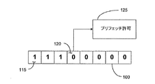
図1Aは、本特許明細書の種々の代表的な実施形態に記載されるようなプリフェッチイネーブルシフトレジスタ100の図である。代表的な実施形態では、プリフェッチイネーブルシフトレジスタ100は、例えば8ビットシフトレジスタとすることができる双方向シフトレジスタ100であり、ここではシフトレジスタ100と呼ぶことにする。シフトレジスタ100は、多数のビット位置115を含み、図1Aでは明瞭に示すために、左側の第1のビットのみが識別番号を付されている。プリフェッチイネーブル検出ビット120は、ここでは予め選択されたビット120とも呼ばれ、代表的な実施例では、シフトレジスタ100の左から4番目のビット位置115である。より一般的には、プリフェッチイネーブル検出位置120は、シフトレジスタ100のn番目のビット位置である。プリフェッチ許可条件125は、図1Aに示されるように、論理0がプリフェッチイネーブル検出ビット120に格納されている限り活性化されている。
【0014】
図1Bは、本特許明細書の種々の代表的な実施形態に記載されるようなプリフェッチイネーブルシフトレジスタ100の別の図である。図1Aに示される状況は、命令アドレスのプリフェッチ後に図1Bの状態になる。図1Bでは、論理1(130)が、左側入力150からプリフェッチイネーブルシフトレジスタ100内にシフトされている。ここでは、論理1がプリフェッチイネーブル検出ビット120に格納されている。図1Bに示されるように、プリフェッチイネーブル検出ビット120に論理1が格納されている限り、プリフェッチ非許可条件135が活性化されている。さらに、プリフェッチイネーブル検出ビット120に論理0が再び格納されるまで、命令アドレスのプリフェッチは防止される。
【0015】
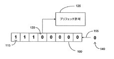
図1Cは、本特許明細書の種々の代表的な実施形態に記載されるようなプリフェッチイネーブルシフトレジスタ100のさらに別の図である。図1Bに示される状況は、キャッシュライン上の最後の命令の実行後に図1Cの状態になる。図1Cでは、論理0(140)が、右側入力155からプリフェッチイネーブルシフトレジスタ100内にシフトされている。ここでは、プリフェッチイネーブル検出ビット120に論理0が格納されている。図1Cに示されるように、プリフェッチイネーブル検出ビット120に論理0が格納されている限り、プリフェッチ許可条件125が再び活性化され、かつそのまま保持される。さらに、論理1がプリフェッチイネーブル検出ビット120に再び格納されるまで、命令アドレスのプリフェッチ処理はイネーブルにされている。プリフェッチ許可条件125をイネーブルにするために、プリフェッチイネーブル検出ビット120において論理0を選択することは典型的ではあるが、任意である。論理0の補数である論理1を選択することもできる。この場合には、命令アドレスのプリフェッチ後に、論理0がプリフェッチイネーブルシフトレジスタ100内にシフトされ、キャッシュライン上での最後の命令の実行後に、論理1がプリフェッチイネーブルシフトレジスタ100内にシフトされる。種々の代表的な実施形態において、左側および右側入力150および155は入れ替えられることに留意されたい。
【0016】
図2は、本特許明細書の種々の代表的な実施形態に記載されるような命令アドレスをプリフェッチするための装置200の図である。装置200は、プリフェッチ命令アドレスレジスタ205と、インクリメンタ(incrementor)215と、プリフェッチイネーブルシフトレジスタ100を含むプロセッサ制御回路210とを備える。また図2には、ターゲット命令アドレス220と、プリフェッチ命令アドレス225と、命令キャッシュ270と、プロセッサ250と、メモリ280と、プログラム記憶媒体290と、プリフェッチ受入信号255と、新規プリフェッチ条件信号260と、キャッシュライン272上の最後の命令がフェッチされたことを示す、キャッシュライン上でフェッチされた最後命令の信号265とが示される。プロセッサ250はここでは、マイクロプロセッサ250とも呼ばれる。命令キャッシュ270は典型的には2つ以上のキャッシュライン272を含み、図2にはそのうちの1つのみが示されており、また各キャッシュライン272は、少なくとも1つの命令のアドレスを含むが、一般的には多数の命令アドレスを含む。別個に示されているが、実際には、プロセッサ250は典型的には、限定はしないが、メモリ280、命令キャッシュ270およびプロセッサ制御回路210を含む、図2に示されるいくつかの構成要素を含んでいる。メモリ280は、プロセッサ250によって実行されるべき命令用の記憶装置、並びにその機能を実行する際にプロセッサ250によって必要とされる他のメモリを含む。プログラム記憶媒体290は、図には示されないが、プリフェッチを実行し、かつ制御するためのソフトウエアプログラム用のメモリ記憶装置を含む。プログラム記憶媒体290は例えば、ハードディスク、フロッピーディスク、ランダムアクセスメモリ(RAM)、リードオンリーメモリ(ROM)あるいは任意の他のコンピュータアクセス可能記憶媒体とすることができる。またプリフェッチ命令アドレスレジスタ205は、アドレスレジスタ205とも呼ばれる。
【0017】
図2では、SET A(230)が論理的に真になる場合、ターゲット命令アドレス220が、プリフェッチ命令アドレスレジスタ205へ書き込まれる。このアドレスを用いて、プリフェッチ処理を開始するための開始メモリ位置を生成する。プリフェッチ条件が新規プリフェッチ条件信号260を介して検出される場合、SET A(230)は論理的に真になる。代表的な実施形態では、プリフェッチ条件は典型的には、プリフェッチ動作を開始するためにプロセッサ制御回路210に命令するソフトウエアにコード化される。この条件が図2に示されており、新規プリフェッチ条件信号260が、プロセッサ250からプロセッサ制御回路210に流れることが示されている。その後、この条件に対応するターゲット命令アドレス220が準備され、プリフェッチ命令アドレスレジスタ205へ書き込まれる。
【0018】
プリフェッチイネーブルシフトレジスタ100のプリフェッチイネーブル検出ビット120に論理0が格納され、かつプリフェッチが、命令キャッシュ270に発行される、または命令キャッシュ270により受け取られる場合、このようなことはプリフェッチ受入信号255によって示されるが、このときSET B(235)が論理的に真になる。その後命令アドレスのプリフェッチ処理は以下のように進む。(1)信号260を介して示される、新しいプリフェッチ条件がプロセッサ250によって検出される場合、開始ターゲット命令アドレス220が、INPUT A(240)を介してプリフェッチ命令アドレスレジスタ205へ書き込まれ、(2)ターゲット命令アドレス220がインクリメンタ215に送出され、(3)インクリメンタ215がその命令アドレスを次の順番のアドレスの値にインクリメントし、(4)信号255を介して示されるプリフェッチが、命令キャッシュ270によって受け入れられる場合、INPUT B(245)を介して、インクリメントされた命令アドレスがプリフェッチ命令アドレスレジスタ205へ書き込まれる。その後、命令アドレスのプリフェッチ処理は、停止プリフェッチ条件と出会うまで、あるいは論理1(130)がプリフェッチイネーブルシフトレジスタ100のプリフェッチイネーブル検出ビット120へ書き込まれるまで、以下のステップを通してループを進み続ける。(1)インクリメントされた命令アドレスがインクリメンタ215に送出され、(2)インクリメンタ215がそのアドレスを次の順番のアドレスの値にインクリメントし、(3)信号255を介して示されるプリフェッチが、命令キャッシュ270によって受け入れられる場合、インクリメントされた命令アドレスが、INPUT B(245)を介してプリフェッチ命令アドレスレジスタ205へ書き込まれる。必要に応じて、プリフェッチ命令アドレス225は、命令キャッシュ270に転送される。プロセッサ250が、信号265を介して示され、命令キャッシュ270においてプロセッサ250によって読み出される、キャッシュライン272上の最後の命令をフェッチした後、右側から論理0(140)が、プリフェッチイネーブルシフトレジスタ100へ書き込まれる。またプロセッサ250は、図2には示されない停止プリフェッチ標識をプロセッサ制御回路210に発行し、プロセッサ制御回路210はプリフェッチ動作を停止する。代表的な実施形態では、命令アドレス225のプリフェッチは順次処理されているが、他の命令アドレスの方式も可能であり、本発明は順次命令アドレスに限定されない。
【0019】
図3は、本特許明細書の種々の代表的な実施形態に記載されるような、命令アドレス300をプリフェッチするための方法の流れ図である。プリフェッチ条件が検出される場合、ブロック305は制御をブロック310に渡す。プリフェッチ条件は、例えば、プリフェッチ処理が分岐ターゲットにおいて開始することを示す特別に符号化された分岐命令を実行することである。実行されるべき命令を生成するソフトウエアは、ターゲットアドレスで開始する命令のブロックがプリフェッチ処理から恩恵を受けるものと決定する場合、分岐に特別な符号化(「hints」のようなIA64アーキテクチャにおいて知られている)を加える。そうでない場合には、ブロック305が繰り返される。
【0020】
ブロック310は、SET A(230)を真に設定することによって、プリフェッチ条件に関連するターゲット命令アドレス220を、プリフェッチ命令アドレスレジスタ205へ書き込む。その後、ブロック310は制御をブロック315に渡す。
【0021】
ブロック315は、プリフェッチイネーブルシフトレジスタ100を初期化する。その例の実施形態では、シフトレジスタ100は8ビット位置を含み、シフトレジスタ100のビット位置115は「10000000」に設定される。その後、ブロック315は制御をブロック320に渡す。
【0022】
プリフェッチイネーブルシフトレジスタ100内のプリフェッチイネーブル検出ビット120(n番目のビット位置120)が論理0に等しく、かつ命令キャッシュ270がプリフェッチの受け入れ準備ができている場合、ブロック320は制御をブロック325に渡す。そうでない場合には、ブロック320は制御をブロック335に渡す。
【0023】
ブロック325は、次の命令アドレスをプリフェッチ命令アドレスレジスタ205へ書き込む。この時点で、SET B(235)は、論理的に真に設定されている。その後ブロック325は制御をブロック330に渡す。
【0024】
ブロック330は、論理1(130)を左側からプリフェッチイネーブルシフトレジスタ100内にシフトする。その後ブロック330は制御をブロック333に渡す。
【0025】
ブロック333は、プリフェッチ命令アドレス225を命令キャッシュ270へ書き込む。その後ブロック333は制御をブロック335に渡す。
【0026】
プロセッサが、命令キャッシュ270のキャッシュライン272上の最後の命令をフェッチする場合、ブロック335は制御をブロック340に渡す。そうでない場合には、ブロック335は制御をブロック345に渡す。
【0027】
ブロック340は、右側から論理0(140)をプリフェッチイネーブルシフトレジスタ100内にシフトする。その後ブロック340は制御をブロック345に渡す。
【0028】
停止プリフェッチ条件が発生するとき、ブロック345は制御をブロック305に渡す。停止プリフェッチ条件は、例えば、分岐を実行して、プリフェッチされていない新しい命令のシーケンスから実行し始めるために、プロセッサを向け直すことである。代表的な実施形態では、ソフトウエアプログラムが行うあらゆる分岐によって、停止プリフェッチ条件が生じるであろう。そうでない場合には、ブロック345は制御をブロック320に渡す。
【0029】
従来のマイクロプロセッサプリフェッチ処理技術より優れた、本特許明細書に記載されるような実施形態の主な利点は、過剰なプリフェッチ処理を排除することである。プロセッサによってフェッチされている命令よりも、必要以上に多くの命令を命令キャッシュ内にプリフェッチすることによって、メモリは無駄にされ、命令キャッシュ内の有用な命令が、一度も使用される可能性のない命令に置き換えられる可能性がある。現在の命令ポインタの前のプリフェッチの数は厳密に制御される。それにより本発明の実施形態は、貴重なシステムリソースを節約する。
【0030】
本発明は好ましい実施形態に関連して詳細に記載されてきたが、記載された実施形態は例示のために示されており、限定するためではない。記載された実施形態の形態および細部に種々の変更を行って、請求の範囲内において等価な実施形態を実現できることは当業者には理解されよう。
【0031】
本発明を要約すると次のようになる。プリフェッチ性能を最適化するための装置(200)と方法である。論理1(130)が左側からシフトレジスタ(100)のビット内へ、プリフェッチされる各命令アドレス(225)毎にシフトされる。命令アドレス(225)がプロセッサによりフェッチされ、論理0(140)が右側からシフトレジスタ(100)のビット位置(115)へシフトされる。一旦、開始されれば、シフトレジスタ(100)のn番目のビット(120)に論理1が格納されるまで、プリフェッチは続行する。n番目のビット(120)の論理1を検出することにより、またプリフェッチされた命令アドレス(225)がプリフェッチ命令アドレスレジスタ(205)から除去され、論理0がシフトレジスタ(100)のn番目のビット(120)へシフトされて戻されるまで、プリフェッチは中断する。従って、自立的なプリフェッチエージェントにより現在の命令ポインタのあまりにも前方でのプリフェッチが防止され、結果として、無駄なメモリバンド幅、及び命令キャッシュ(270)の有用な命令の置換が防止される。
【0032】
以下においては、本発明の種々の構成要件の組み合わせからなる例示的な実施態様を示す。
1.コンピュータによって実行可能な命令からなるソフトウエアプログラムを具体的に組み入れ、コンピュータによって読出し可能なコンピュータプログラム記憶媒体(290)であって、前記コンピュータが、命令アドレス(225)をプリフェッチするための方法を実行するためのマイクロプロセッサ(250)を含み、前記命令アドレスをプリフェッチするための方法が、
シフトレジスタ(100)内の予め選択されたビット位置(120)が予め選択された論理値(140)に設定され、かつ前記マイクロプロセッサ(250)が、プリフェッチ命令アドレス(225)の受け入れ準備ができているとき、
前記プリフェッチ命令アドレス(225)をアドレスレジスタ(205)へ書き込むステップと、
前記プリフェッチ命令アドレス(225)を命令キャッシュ(270)へ書き込むステップと、
前記プリフェッチ命令アドレス(225)を、次のプリフェッチ命令アドレス(225)のアドレスの値にインクリメントするステップと、
前記命令キャッシュ(270)が前記プリフェッチ命令アドレス(225)を受け入れたとき、
前記シフトレジスタ(100)が左側入力(150)と右側入力(155)とを有し、各入力(150、155)が前記シフトレジスタ(100)内に論理値(130、140)をシフトする能力を有していて、前記予め選択された論理値(140)の補数(130)を前記左側入力(150)において前記シフトレジスタ(100)内にシフトするステップと、
前記マイクロプロセッサ(250)が前記命令キャッシュ(270)内のキャッシュライン(272)からの最後の命令をフェッチするとき、前記予め選択された論理値(140)に等しい値を、前記右側入力(155)において前記シフトレジスタ(100)内にシフトするステップとを含む、コンピュータプログラム記憶媒体(290)。
2.前記方法が、
上記1に記載のステップの前に、かつプリフェッチ条件(260)がプロセッサ制御回路(210)によって検出されたときに、
前記プリフェッチ条件(260)に関連するターゲット命令アドレス(220)を、前記アドレスレジスタ(205)へ書き込むステップと、及び
前記左側入力(150)に接続されたビット位置(115)において前記予め選択された論理値(140)の補数に、かつ前記シフトレジスタ(100)の他の全てのビット位置(115)において前記予め選択された論理値(140)に、前記シフトレジスタ(100)を初期化するステップとをさらに含む、上記1に記載のコンピュータプログラム記憶媒体(290)。
3.前記方法が、
停止プリフェッチ条件(345)が発生するとき、命令アドレス(225)のプリフェッチ処理を終了するステップをさらに含む、上記2に記載のコンピュータプログラム記憶媒体(290)。
4.前記予め選択された論理値(140)が論理0であり、前記予め選択された論理値(140)の補数(130)が論理1である、上記2に記載のコンピュータプログラム記憶媒体(290)。
5.前記予め選択された論理値(140)が論理1であり、前記予め選択された論理値(140)の補数(130)が論理0である、上記2に記載のコンピュータプログラム記憶媒体(290)。
6.命令アドレス(225)をプリフェッチするためのコンピュータが使用可能な方法であって、
シフトレジスタ(100)内の予め選択されたビット位置(120)が予め選択された論理値(140)に設定され、マイクロプロセッサ(250)が、前記プリフェッチ命令アドレス(225)を受け入れる準備ができているとき、
前記プリフェッチ命令アドレス(225)をアドレスレジスタ(205)へ書き込むステップと、
前記プリフェッチ命令アドレス(225)を命令キャッシュ(270)へ書き込むステップと、
前記プリフェッチ命令アドレス(225)を、次のプリフェッチ命令アドレス(225)のアドレスの値にインクリメントするステップと、
前記命令キャッシュ(270)が前記プリフェッチ命令アドレス(225)を受け入れたとき、
前記シフトレジスタ(100)が左側入力(150)と右側入力(155)とを有し、各入力(150、155)が前記シフトレジスタ(100)内に前記論理値(130、140)をシフトする能力を有していて、前記予め選択された論理値(140)の補数(130)を前記左側入力(150)において前記シフトレジスタ(100)内にシフトするステップと、
前記マイクロプロセッサ(250)が前記命令キャッシュ(270)内のキャッシュライン(272)からの最後の命令をフェッチするとき、前記予め選択された論理値(140)に等しい値を、前記右側入力(155)において前記シフトレジスタ(100)内にシフトするステップとを含む、コンピュータが使用可能な方法。
7.前記方法が、
上記6に記載のステップの前に、かつプリフェッチ条件(260)がプロセッサ制御回路(210)によって検出されたとき、
前記プリフェッチ条件(260)に関連するターゲット命令アドレス(220)を、前記アドレスレジスタ(205)へ書き込むステップと、
前記左側入力(150)に接続されたビット位置(115)において前記予め選択された論理値(140)の補数に、かつ前記シフトレジスタ(100)の他の全てのビット位置(115)において前記予め選択された論理値(140)に、前記シフトレジスタ(100)を初期化するステップとをさらに含む、上記6に記載のコンピュータが使用可能な方法。
8.前記方法が、
停止プリフェッチ条件(345)が発生するとき、命令アドレス(225)のプリフェッチ処理を終了するステップをさらに含む、上記7に記載のコンピュータが使用可能な方法。
9.前記予め選択された論理値(140)が論理0であり、前記予め選択された論理値(140)の補数(130)が論理1である、上記7に記載のコンピュータが使用可能な方法。
10.命令アドレス(225)をプリフェッチするための装置(200)であって、
入力および出力を有するインクリメンタ(215)と、
SET A(230)およびSET B(235)制御ポートと、入力INPUT A(240)およびINPUT B(245)と、出力とを有するアドレスレジスタ(205)であって、そのアドレスレジスタ(205)の前記出力は、前記インクリメンタ(215)の前記入力に接続され、前記インクリメンタ(215)の前記出力は前記INPUT B(245)に接続される、アドレスレジスタ(205)と、
左側入力(150)と、右側入力(155)と、2つ以上のビット位置(115)とを含むシフトレジスタ(100)であって、そのシフトレジスタ(100)は、SET B(235)を介して前記アドレスレジスタ(205)に接続され、各入力(150、155)が、論理値(130、140)を前記シフトレジスタ(100)内にシフトする能力を有し、プロセッサ制御回路(210)によってプリフェッチ条件(260)が検出されたとき、前記アドレスレジスタ(205)は前記INPUT A(240)を介して、前記プリフェッチ条件(260)に関連するターゲット命令アドレス(220)を受け入れる能力を有しており、前記シフトレジスタ(100)が、前記左側入力(150)に接続されるビット位置(115)を前記予め選択された論理値(140)の補数(130)に、かつ前記シフトレジスタ(100)の全ての他のビット位置(115)を前記予め選択された論理値(140)に初期化されることができ、前記シフトレジスタ(100)内の予め選択されたビット位置(120)が前記予め選択された論理値(140)に設定され、かつマイクロプロセッサ(250)が前記プリフェッチ命令アドレス(225)を受け入れる準備ができているとき、前記SET B(235)が前記アドレスレジスタ(205)に格納されたアドレスの前記インクリメンタ(215)によるインクリメントをイネーブルにし、命令キャッシュ(270)が前記プリフェッチ命令アドレス(225)を受け入れたとき、前記シフトレジスタ(100)は前記予め選択された論理値(140)の前記補数(130)を前記左側入力(150)において前記シフトレジスタ(100)内にシフトする能力を有し、前記マイクロプロセッサ(250)が前記命令キャッシュ(270)のキャッシュライン(272)からの最後の命令をフェッチするとき、前記シフトレジスタ(100)は、前記予め選択された論理値(140)に等しい値を、前記右側入力(155)において前記シフトレジスタ(100)内にシフトする能力を有する、シフトレジスタ(100)とを含む、装置(200)。
【0033】
【発明の効果】
本発明によれば、プリフェッチ処理を最適化することによりメモリバンド幅のようなリソースを無駄にし、命令キャッシュ内の有用な命令を置き換えてしまうことなく、命令フェッチにおけるキャッシュミスを防ぐことができる。
【図面の簡単な説明】
【図1A】本特許明細書の種々の代表的な実施形態に記載されるようなプリフェッチイネーブルシフトレジスタの図である。
【図1B】本特許明細書の種々の代表的な実施形態に記載されるようなプリフェッチイネーブルシフトレジスタの別の図である。
【図1C】本特許明細書の種々の代表的な実施形態に記載されるようなプリフェッチイネーブルシフトレジスタのさらに別の図である。
【図2】本特許明細書の種々の代表的な実施形態に記載されるような命令アドレスプリフェッチのための装置の図である。
【図3】本特許明細書の種々の代表的な実施形態に記載されるような命令アドレスをプリフェッチするための方法を示す流れ図である。
【符号の説明】
100 プリフェッチイネーブルシフトレジスタ
115 ビット位置
120 プリフェッチイネーブル検出ビット
130 補数
140 論理0
150 左側入力
155 右側入力
200 装置
205 プリフェッチ命令アドレスレジスタ
210 プロセッサ制御回路
220 ターゲット命令アドレス
225 プリフェッチ命令アドレス
230 SET A
235 SET B
240 INPUT A
245 INPUT B
250 マイクロプロセッサ
260 プリフェッチ条件信号
270 命令キャッシュ
272 キャッシュライン
290 コンピュータプログラム記憶媒体[0001]
BACKGROUND OF THE INVENTION
The present invention relates to microprocessors, and more particularly to a method and apparatus for optimizing prefetch performance.
[0002]
[Prior art]
Modern microprocessors typically perform instruction prefetch processing. Prefetch processing is a mechanism for the processor hardware to attempt to load or prefetch (prefetch) instructions from a higher level of the cache or from memory into the instruction cache. If the instruction cache is loaded before the processor fetches the instruction, there will be no cache miss and associated performance penalty. Each of these prefetch operations will attempt to load multiple instructions into the instruction cache. The number of instructions so loaded is typically equal to the number of instructions in the cache line. A cache line is defined as the basic amount of data that can be read from or written to the cache.
[0003]
Instruction prefetch is initiated by a program via a prefetch instruction, by hardware, or a combination of both. Prefetch may attempt to load just a few instructions or may load a long sequence of instructions. Problems can arise when prefetching long sequences of instructions. Specifically, instructions that are not executed due to control flow changes or branches may be prefetched. In this situation, performance can be degraded for two reasons. First, each prefetch must use processor and system resources such as higher level caches, system buses and memory units. If these resources are used by prefetching, other operations, such as load or store operations, will not be able to use them. Second, when instructions are prefetched into the instruction cache, memory space for those instructions must be created by overwriting existing instructions. These existing instructions may form part of the working set, i.e., they may be needed by the processor in the near future. Thus, excessive prefetch processing that occurs when a large number of instructions are prefetched into the instruction cache, but not yet fetched by the processor, wastes resources, and useful instructions in the instruction cache are used once. There is a possibility of being replaced by an instruction that never happens.
[0004]
Therefore, there is a need to limit the number of instructions that are prefetched before the processor is fetching instructions from the current instruction pointer. It would be desirable and would be a great advantage to provide a mechanism that allows the processor to prefetch at a certain distance before the instruction pointer.
[0005]
[Problems to be solved by the invention]
Such prefetching helps to hide the latency of the fetching process, prefetches too forward, wastes resources such as memory bandwidth, and replaces useful instructions in the instruction cache. It is to prevent cache misses in instruction fetches.
[0006]
[Means for Solving the Problems]
In an exemplary embodiment, the present invention provides a method and apparatus for controlling the ratio of instruction address prefetch by a microprocessor. Previous methods for prefetch processing are not focused on limiting the number of instructions prefetched before the processor is fetching instructions from the current instruction pointer, which wastes memory bandwidth. This has created the possibility of replacing useful instructions in the instruction cache.
[0007]
In an exemplary embodiment, the bits in the shift register are used to count the number of instruction addresses that are prefetched. When an instruction prefetch address is issued to the processor, the prefetched address is added to the register and a logic “1” is shifted into the shift register from the left side. By issuing each prefetch to the processor, the instruction cache line is written to the instruction cache. When the last prefetched instruction on the cache line is fetched, a logic “0” is shifted into the shift register from the right. When a
[0008]
The main advantage of the embodiments described in this patent document over the conventional microprocessor prefetch processing technique is that excessive prefetch processing is eliminated. By prefetching more instructions into the instruction cache than needed by the processor, resources such as memory bandwidth are wasted and useful instructions in the instruction cache are used once. May be replaced by instructions that may never happen. The number of prefetches before the current instruction pointer is strictly controlled. Thereby, embodiments of the present invention save valuable system resources.
[0009]
DETAILED DESCRIPTION OF THE INVENTION
Other aspects and advantages of the present invention will become apparent from the following detailed description, taken in conjunction with the accompanying drawings, illustrating by way of example the principles of the invention.
[0010]
The accompanying drawings are used to more fully describe the present invention and provide a visual representation that can be used by those skilled in the art to better understand the present invention and its inherent advantages. In these drawings, like reference numbers identify corresponding components.
[0011]
As shown in the drawings for purposes of illustration, this patent specification relates to a novel method for controlling the ratio of instruction address prefetch by a microprocessor. Previous methods for prefetch processing are not focused on limiting the number of instructions prefetched before the processor is fetching instructions from the current instruction pointer, which wastes memory bandwidth. This has created the possibility of replacing useful instructions in the instruction cache. In the following detailed description and in the several drawings, like components are identified with like reference numerals.
[0012]
In an exemplary embodiment, the bits in the shift register are used to count the number of instruction addresses that have been prefetched but not yet fetched by the processor. When an instruction prefetch address is issued to the processor, a logic “1” is shifted into the shift register from the left. By issuing each prefetch to the processor, the instruction cache line is written to the instruction cache. When the last instruction on the cache line is fetched, a logic “0” is shifted into the shift register from the right. When a
[0013]
FIG. 1A is a diagram of a prefetch enable
[0014]
FIG. 1B is another diagram of a prefetch enable
[0015]
FIG. 1C is yet another diagram of a prefetch enable
[0016]
FIG. 2 is a diagram of an
[0017]
In FIG. 2, when SET A (230) is logically true, the
[0018]
This is indicated by a prefetch accept
[0019]
FIG. 3 is a flowchart of a method for prefetching an
[0020]
[0021]
[0022]
If the prefetch enable detect bit 120 (nth bit position 120) in the prefetch enable
[0023]
[0024]
[0025]
[0026]
If the processor fetches the last instruction on
[0027]
[0028]
Block 345 passes control to block 305 when a stop prefetch condition occurs. A stop prefetch condition is, for example, to execute a branch and redirect the processor to begin execution from a new sequence of instructions that has not been prefetched. In the exemplary embodiment, every branch taken by the software program will cause a stop prefetch condition. Otherwise, block 345 passes control to block 320.
[0029]
The main advantage of the embodiments as described in this patent, over conventional microprocessor prefetch processing techniques, is to eliminate excessive prefetch processing. By prefetching more instructions than necessary into the instruction cache than the instructions being fetched by the processor, memory is wasted and useful instructions in the instruction cache can never be used. May be replaced with an instruction. The number of prefetches before the current instruction pointer is strictly controlled. Thereby, embodiments of the present invention save valuable system resources.
[0030]
Although the present invention has been described in detail in connection with the preferred embodiments, the described embodiments are shown by way of illustration and not limitation. Those skilled in the art will recognize that various modifications can be made to the form and details of the described embodiments to achieve equivalent embodiments within the scope of the claims.
[0031]
The present invention is summarized as follows. An apparatus (200) and method for optimizing prefetch performance. A logic 1 (130) is shifted from the left into the bits of the shift register (100) for each prefetched instruction address (225). The instruction address (225) is fetched by the processor, and a logical 0 (140) is shifted from the right side to the bit position (115) of the shift register (100). Once started, prefetching continues until a
[0032]
In the following, exemplary embodiments consisting of combinations of various constituents of the present invention are shown.
1. A computer program storage medium (290) that specifically incorporates a software program comprising instructions executable by a computer and that is readable by the computer, the computer performing a method for prefetching an instruction address (225) Including a microprocessor (250) for prefetching the instruction address,
The preselected bit position (120) in the shift register (100) is set to a preselected logic value (140) and the microprocessor (250) is ready to accept the prefetch instruction address (225). When
Writing the prefetch instruction address (225) to an address register (205);
Writing the prefetch instruction address (225) to an instruction cache (270);
Incrementing the prefetch instruction address (225) to the address value of the next prefetch instruction address (225);
When the instruction cache (270) accepts the prefetch instruction address (225),
The shift register (100) has a left input (150) and a right input (155), and each input (150, 155) is capable of shifting a logic value (130, 140) into the shift register (100). Shifting the complement (130) of the preselected logic value (140) into the shift register (100) at the left input (150);
When the microprocessor (250) fetches the last instruction from the cache line (272) in the instruction cache (270), a value equal to the preselected logic value (140) is entered into the right input (155 ) In the shift register (100).
2. The method comprises
Before the step described in 1 above and when a prefetch condition (260) is detected by the processor control circuit (210),
Writing a target instruction address (220) associated with the prefetch condition (260) to the address register (205); and
In the bit position (115) connected to the left input (150) the complement of the preselected logic value (140) and in all other bit positions (115) of the shift register (100) The computer program storage medium (290) of
3. The method comprises
The computer program storage medium (290) of claim 2, further comprising the step of ending the prefetch processing of the instruction address (225) when the stop prefetch condition (345) occurs.
4). The computer program storage medium (290) of claim 2, wherein the preselected logical value (140) is a logical 0 and the complement (130) of the preselected logical value (140) is a logical one.
5. The computer program storage medium (290) of claim 2, wherein the preselected logical value (140) is a logical one and the complement (130) of the preselected logical value (140) is a logical zero.
6). A computer usable method for prefetching an instruction address (225) comprising:
The preselected bit position (120) in the shift register (100) is set to a preselected logic value (140) and the microprocessor (250) is ready to accept the prefetch instruction address (225). When
Writing the prefetch instruction address (225) to an address register (205);
Writing the prefetch instruction address (225) to an instruction cache (270);
Incrementing the prefetch instruction address (225) to the address value of the next prefetch instruction address (225);
When the instruction cache (270) accepts the prefetch instruction address (225),
The shift register (100) has a left input (150) and a right input (155), and each input (150, 155) shifts the logical value (130, 140) into the shift register (100). Shifting the complement (130) of the preselected logic value (140) into the shift register (100) at the left input (150), having the capability;
When the microprocessor (250) fetches the last instruction from the cache line (272) in the instruction cache (270), a value equal to the preselected logic value (140) is entered into the right input (155 ) In the shift register (100).
7). The method comprises
Before the step described in 6 above and when the prefetch condition (260) is detected by the processor control circuit (210),
Writing a target instruction address (220) associated with the prefetch condition (260) to the address register (205);
In the bit position (115) connected to the left input (150) the complement of the preselected logic value (140) and in all other bit positions (115) of the shift register (100) 7. The computer usable method of claim 6, further comprising initializing the shift register (100) to a selected logical value (140).
8). The method comprises
8. The computer usable method of claim 7, further comprising the step of ending the prefetch processing of the instruction address (225) when the stop prefetch condition (345) occurs.
9. 8. The computer usable method of claim 7, wherein the preselected logical value (140) is a logical zero and the complement (130) of the preselected logical value (140) is a logical one.
10. A device (200) for prefetching an instruction address (225),
An incrementer (215) having an input and an output;
An address register (205) having a SET A (230) and SET B (235) control port, an input INPUT A (240) and an INPUT B (245), and an output of the address register (205) An output connected to the input of the incrementer (215), the output of the incrementer (215) connected to the INPUT B (245), an address register (205);
A shift register (100) including a left input (150), a right input (155), and two or more bit positions (115), the shift register (100) being routed through a SET B (235) Connected to the address register (205), and each input (150, 155) has the ability to shift logical values (130, 140) into the shift register (100), and is controlled by the processor control circuit (210) When a prefetch condition (260) is detected, the address register (205) has the ability to accept a target instruction address (220) associated with the prefetch condition (260) via the INPUT A (240). The shift register (100) sets the bit position (115) connected to the left input (150) to the complement (130) of the preselected logic value (140), and the shift register (100) All other Can be initialized to the preselected logic value (140), and the preselected bit position (120) in the shift register (100) can be initialized to the preselected logic value (140). When set to the value (140) and the microprocessor (250) is ready to accept the prefetch instruction address (225), the SET B (235) is stored in the address register (205). When increment by the incrementer (215) is enabled and the instruction cache (270) accepts the prefetch instruction address (225), the shift register (100) is the complement of the preselected logic value (140). (130) has the ability to shift into the shift register (100) at the left input (150), the microprocessor (250) When fetching the last instruction from the cache line (272) of the cache (270), the shift register (100) sets a value equal to the preselected logic value (140) at the right input (155). A device (200) comprising a shift register (100) having the ability to shift into the shift register (100).
[0033]
【The invention's effect】
According to the present invention, it is possible to prevent a cache miss in an instruction fetch without wasting resources such as memory bandwidth by optimizing the prefetch process and replacing a useful instruction in the instruction cache.
[Brief description of the drawings]
FIG. 1A is a diagram of a prefetch enable shift register as described in various exemplary embodiments of this patent specification.
FIG. 1B is another diagram of a prefetch enable shift register as described in various representative embodiments of this patent specification.
FIG. 1C is yet another diagram of a prefetch enable shift register as described in various representative embodiments of this patent specification.
FIG. 2 is an illustration of an apparatus for instruction address prefetch as described in various representative embodiments of this patent specification.
FIG. 3 is a flow diagram illustrating a method for prefetching an instruction address as described in various exemplary embodiments of this patent specification.
[Explanation of symbols]
100 prefetch enable shift register
115 bit position
120 Prefetch enable detection bit
130's complement
140
150 Left input
155 Right input
200 devices
205 Prefetch instruction address register
210 Processor control circuit
220 Target instruction address
225 Prefetch instruction address
230 SET A
235 SET B
240 INPUT A
245 INPUT B
250 microprocessor
260 Prefetch condition signal
270 instruction cache
272 cash line
290 Computer program storage media
Claims (3)
シフトレジスタ内の予め選択されたビット位置が予め選択された論理値に設定され、かつ前記マイクロプロセッサが、プリフェッチ命令アドレスの受け入れ準備ができているとき、
前記プリフェッチ命令アドレスをアドレスレジスタへ書き込むステップと、
プリフェッチが命令キャッシュに発行されるステップと、
前記プリフェッチ命令アドレスを、次のプリフェッチ命令アドレスのアドレスの値にインクリメントするステップと、
前記命令キャッシュが前記プリフェッチを実行したとき、
前記シフトレジスタが左側入力と右側入力とを有し、各入力が前記シフトレジスタ内に論理値をシフトする能力を有していて、前記予め選択された論理値の補数を前記左側入力において前記シフトレジスタ内にシフトするステップと、
前記マイクロプロセッサが前記命令キャッシュ内のキャッシュラインからの最後の命令をフェッチするとき、前記予め選択された論理値に等しい値を、前記右側入力において前記シフトレジスタ内にシフトするステップとを含む、コンピュータプログラム記憶媒体。 Set look put software program of instructions executable by a computer, a readable computer program storage medium by a computer, includes a microprocessor for the computer to perform a method for prefetching instruction , a method for pre-fetching the instruction is,
When a preselected bit position in the shift register is set to a preselected logic value and the microprocessor is ready to accept a prefetch instruction address;
Writing the prefetch instruction address to an address register;
A step flop Rife' switch is issued to the instruction cache,
Incrementing the prefetch instruction address to the value of the address of the next prefetch instruction address;
When said instruction cache executes the prefetching,
The shift register has a left input and a right input, each input having the ability to shift a logic value into the shift register, and the complement of the preselected logic value is shifted at the left input. Shifting into a register;
Shifting the value equal to the preselected logic value into the shift register at the right input when the microprocessor fetches the last instruction from a cache line in the instruction cache. Program storage medium.
シフトレジスタ内の予め選択されたビット位置が予め選択された論理値に設定され、マイクロプロセッサが、プリフェッチ命令アドレスを受け入れる準備ができているとき、
前記プリフェッチ命令アドレスをアドレスレジスタへ書き込むステップと、
プリフェッチが命令キャッシュに発行されるステップと、
前記プリフェッチ命令アドレスを、次のプリフェッチ命令アドレスのアドレスの値にインクリメントするステップと、
前記命令キャッシュがプリフェッチを実行したとき、
前記シフトレジスタが左側入力と右側入力とを有し、各入力が前記シフトレジスタ内に前記論理値をシフトする能力を有していて、前記予め選択された論理値の補数を前記左側入力において前記シフトレジスタ内にシフトするステップと、
前記マイクロプロセッサが前記命令キャッシュ内のキャッシュラインからの最後の命令をフェッチするとき、前記予め選択された論理値に等しい値を、前記右側入力において前記シフトレジスタ内にシフトするステップとを含む、コンピュータが使用可能な方法。Computer for prefetching instruction is an available method,
Preselected bit positions in the shift register is set to a preselected logic value, when the microprocessor is ready to accept a prefetch instruction address,
Writing the prefetch instruction address to an address register;
A step flop Rife' switch is issued to the instruction cache,
Incrementing the prefetch instruction address to the value of the address of the next prefetch instruction address;
When executing the instruction cache Gapu Rife' Ji,
The shift register has a left input and a right input, each input having the ability to shift the logic value into the shift register, and the complement of the preselected logic value at the left input Shifting into a shift register;
Shifting the value equal to the preselected logic value into the shift register at the right input when the microprocessor fetches the last instruction from a cache line in the instruction cache. Can be used.
入力および出力を有するインクリメンタと、
SET AおよびSET B制御ポートと、入力INPUT AおよびINPUT Bと、出力とを有するアドレスレジスタであって、そのアドレスレジスタの前記出力は、前記インクリメンタの前記入力に接続され、前記インクリメンタの前記出力は前記INPUT Bに接続される、アドレスレジスタと、
左側入力と、右側入力と、2つ以上のビット位置とを含むシフトレジスタであって、そのシフトレジスタは、SET Bを介して前記アドレスレジスタに接続され、各入力が、論理値を前記シフトレジスタ内にシフトする能力を有し、プロセッサ制御回路によってプリフェッチ条件が検出されたとき、前記アドレスレジスタは前記INPUT Aを介して、前記プリフェッチ条件に関連するターゲット命令アドレスを受け入れる能力を有しており、前記シフトレジスタが、前記左側入力に接続されるビット位置を前記予め選択された論理値の補数に、かつ前記シフトレジスタの全ての他のビット位置を前記予め選択された論理値に初期化されることができ、前記シフトレジスタ内の予め選択されたビット位置が前記予め選択された論理値に設定され、かつマイクロプロセッサが前記プリフェッチ命令アドレスを受け入れる準備ができているとき、前記SET Bが前記アドレスレジスタに格納されたアドレスの前記インクリメンタによるインクリメントをイネーブルにし、命令キャッシュがプリフェッチを実行したとき、前記シフトレジスタは前記予め選択された論理値の前記補数を前記左側入力において前記シフトレジスタ内にシフトする能力を有し、前記マイクロプロセッサが前記命令キャッシュのキャッシュラインからの最後の命令をフェッチするとき、前記シフトレジスタは、前記予め選択された論理値に等しい値を、前記右側入力において前記シフトレジスタ内にシフトする能力を有する、シフトレジスタとを含む、命令をプリフェッチするための装置。An apparatus for prefetch instruction,
An incrementer having an input and an output;
An address register having a SET A and SET B control port, inputs INPUT A and INPUT B, and an output, the output of the address register being connected to the input of the incrementer, An output connected to the INPUT B, an address register;
A shift register including a left input, a right input, and two or more bit positions, the shift register being connected to the address register via SET B, each input having a logical value in the shift register The address register has the ability to accept a target instruction address associated with the prefetch condition via the INPUT A when a prefetch condition is detected by the processor control circuit; The shift register initializes the bit position connected to the left input to the complement of the preselected logic value and all other bit positions of the shift register to the preselected logic value. And the preselected bit position in the shift register is set to the preselected logic value. Is, and when ready to microprocessor receiving said prefetch instruction address is made, the SET B is to enable incrementing by said incrementer of address stored in said address register, perform the instruction cache Gapu Rife' Ji The shift register has the ability to shift the complement of the pre-selected logic value into the shift register at the left input, and the microprocessor can store the last instruction from the cache line of the instruction cache. when fetching, the shift register is a value equal to said preselected logical value has the ability to shift the shift register in the right input, and a shift register, instruction apparatus for prefetching .
Applications Claiming Priority (2)
| Application Number | Priority Date | Filing Date | Title |
|---|---|---|---|
| US09/506,972 US6647487B1 (en) | 2000-02-18 | 2000-02-18 | Apparatus and method for shift register rate control of microprocessor instruction prefetches |
| US09/506972 | 2000-02-18 |
Publications (3)
| Publication Number | Publication Date |
|---|---|
| JP2001236220A JP2001236220A (en) | 2001-08-31 |
| JP2001236220A5 JP2001236220A5 (en) | 2006-11-24 |
| JP4195778B2 true JP4195778B2 (en) | 2008-12-10 |
Family
ID=24016755
Family Applications (1)
| Application Number | Title | Priority Date | Filing Date |
|---|---|---|---|
| JP2001041237A Expired - Fee Related JP4195778B2 (en) | 2000-02-18 | 2001-02-19 | Apparatus and method for instruction prefetch amount control of microprocessor |
Country Status (2)
| Country | Link |
|---|---|
| US (1) | US6647487B1 (en) |
| JP (1) | JP4195778B2 (en) |
Families Citing this family (7)
| Publication number | Priority date | Publication date | Assignee | Title |
|---|---|---|---|---|
| US6973542B1 (en) * | 2000-07-18 | 2005-12-06 | International Business Machines Corporation | Detecting when to prefetch inodes and then prefetching inodes in parallel |
| CN100353346C (en) * | 2002-09-20 | 2007-12-05 | 联发科技股份有限公司 | Embedding system and instruction prefetching device and method thereof |
| JP2004192021A (en) * | 2002-12-06 | 2004-07-08 | Renesas Technology Corp | Microprocessor |
| US7337483B2 (en) * | 2004-01-23 | 2008-03-04 | Allen Medical Systems, Inc. | Surgical positioning apparatus |
| US7707359B2 (en) * | 2005-12-09 | 2010-04-27 | Oracle America, Inc. | Method and apparatus for selectively prefetching based on resource availability |
| KR101360221B1 (en) * | 2007-09-13 | 2014-02-10 | 삼성전자주식회사 | Method of managing instruction cache and processor using the method |
| US10528352B2 (en) | 2016-03-08 | 2020-01-07 | International Business Machines Corporation | Blocking instruction fetching in a computer processor |
Family Cites Families (5)
| Publication number | Priority date | Publication date | Assignee | Title |
|---|---|---|---|---|
| US5473756A (en) * | 1992-12-30 | 1995-12-05 | Intel Corporation | FIFO buffer with full/empty detection by comparing respective registers in read and write circular shift registers |
| JP2621772B2 (en) * | 1993-10-29 | 1997-06-18 | 日本電気株式会社 | Serial transmission device |
| US5819079A (en) * | 1995-09-11 | 1998-10-06 | Intel Corporation | Instruction fetch on demand for uncacheable memory which avoids memory mapped I/O side effects in a processor with speculative instruction fetch |
| US5987539A (en) * | 1996-06-05 | 1999-11-16 | Compaq Computer Corporation | Method and apparatus for flushing a bridge device read buffer |
| US5809566A (en) * | 1996-08-14 | 1998-09-15 | International Business Machines Corporation | Automatic cache prefetch timing with dynamic trigger migration |
-
2000
- 2000-02-18 US US09/506,972 patent/US6647487B1/en not_active Expired - Lifetime
-
2001
- 2001-02-19 JP JP2001041237A patent/JP4195778B2/en not_active Expired - Fee Related
Also Published As
| Publication number | Publication date |
|---|---|
| US6647487B1 (en) | 2003-11-11 |
| JP2001236220A (en) | 2001-08-31 |
Similar Documents
| Publication | Publication Date | Title |
|---|---|---|
| US5941981A (en) | System for using a data history table to select among multiple data prefetch algorithms | |
| CA1204219A (en) | Method and apparatus for prefetching instructions | |
| US6134634A (en) | Method and apparatus for preemptive cache write-back | |
| US5829028A (en) | Data cache configured to store data in a use-once manner | |
| US6088789A (en) | Prefetch instruction specifying destination functional unit and read/write access mode | |
| US6665776B2 (en) | Apparatus and method for speculative prefetching after data cache misses | |
| US20200364054A1 (en) | Processor subroutine cache | |
| US6401192B1 (en) | Apparatus for software initiated prefetch and method therefor | |
| JP2906315B2 (en) | Method and circuit for storing instructions in a cache memory | |
| US6910104B2 (en) | Icache-based value prediction mechanism | |
| US5666505A (en) | Heuristic prefetch mechanism and method for computer system | |
| KR100638935B1 (en) | Processor with memory and data prefetch unit | |
| JP4195778B2 (en) | Apparatus and method for instruction prefetch amount control of microprocessor | |
| KR101049319B1 (en) | Method and apparatus for reducing lookups in branch target address cache | |
| US6851033B2 (en) | Memory access prediction in a data processing apparatus | |
| US20090240914A1 (en) | Recycling long multi-operand instructions | |
| US20040225866A1 (en) | Branch prediction in a data processing system | |
| US6769057B2 (en) | System and method for determining operand access to data | |
| JP3830236B2 (en) | Method and data processing system for using quick decode instructions | |
| US5724533A (en) | High performance instruction data path | |
| US7343481B2 (en) | Branch prediction in a data processing system utilizing a cache of previous static predictions | |
| KR20000003930A (en) | Instruction patch apparatus for decreasing loss when being instruction cache miss | |
| KR100265332B1 (en) | Branch prediction method | |
| US20070239939A1 (en) | Apparatus for Performing Stream Prefetch within a Multiprocessor System | |
| JPH10187531A (en) | Prefetch system for cache memory |
Legal Events
| Date | Code | Title | Description |
|---|---|---|---|
| A521 | Written amendment |
Free format text: JAPANESE INTERMEDIATE CODE: A523 Effective date: 20061006 |
|
| A621 | Written request for application examination |
Free format text: JAPANESE INTERMEDIATE CODE: A621 Effective date: 20061006 |
|
| A977 | Report on retrieval |
Free format text: JAPANESE INTERMEDIATE CODE: A971007 Effective date: 20080604 |
|
| A131 | Notification of reasons for refusal |
Free format text: JAPANESE INTERMEDIATE CODE: A131 Effective date: 20080617 |
|
| A521 | Written amendment |
Free format text: JAPANESE INTERMEDIATE CODE: A523 Effective date: 20080819 |
|
| TRDD | Decision of grant or rejection written | ||
| A01 | Written decision to grant a patent or to grant a registration (utility model) |
Free format text: JAPANESE INTERMEDIATE CODE: A01 Effective date: 20080909 |
|
| A01 | Written decision to grant a patent or to grant a registration (utility model) |
Free format text: JAPANESE INTERMEDIATE CODE: A01 |
|
| A61 | First payment of annual fees (during grant procedure) |
Free format text: JAPANESE INTERMEDIATE CODE: A61 Effective date: 20080929 |
|
| R150 | Certificate of patent or registration of utility model |
Ref document number: 4195778 Country of ref document: JP Free format text: JAPANESE INTERMEDIATE CODE: R150 Free format text: JAPANESE INTERMEDIATE CODE: R150 |
|
| FPAY | Renewal fee payment (event date is renewal date of database) |
Free format text: PAYMENT UNTIL: 20111003 Year of fee payment: 3 |
|
| FPAY | Renewal fee payment (event date is renewal date of database) |
Free format text: PAYMENT UNTIL: 20111003 Year of fee payment: 3 |
|
| S111 | Request for change of ownership or part of ownership |
Free format text: JAPANESE INTERMEDIATE CODE: R313113 |
|
| FPAY | Renewal fee payment (event date is renewal date of database) |
Free format text: PAYMENT UNTIL: 20111003 Year of fee payment: 3 |
|
| R350 | Written notification of registration of transfer |
Free format text: JAPANESE INTERMEDIATE CODE: R350 |
|
| FPAY | Renewal fee payment (event date is renewal date of database) |
Free format text: PAYMENT UNTIL: 20121003 Year of fee payment: 4 |
|
| R250 | Receipt of annual fees |
Free format text: JAPANESE INTERMEDIATE CODE: R250 |
|
| FPAY | Renewal fee payment (event date is renewal date of database) |
Free format text: PAYMENT UNTIL: 20131003 Year of fee payment: 5 |
|
| R250 | Receipt of annual fees |
Free format text: JAPANESE INTERMEDIATE CODE: R250 |
|
| R250 | Receipt of annual fees |
Free format text: JAPANESE INTERMEDIATE CODE: R250 |
|
| R250 | Receipt of annual fees |
Free format text: JAPANESE INTERMEDIATE CODE: R250 |
|
| R250 | Receipt of annual fees |
Free format text: JAPANESE INTERMEDIATE CODE: R250 |
|
| R250 | Receipt of annual fees |
Free format text: JAPANESE INTERMEDIATE CODE: R250 |
|
| R250 | Receipt of annual fees |
Free format text: JAPANESE INTERMEDIATE CODE: R250 |
|
| R250 | Receipt of annual fees |
Free format text: JAPANESE INTERMEDIATE CODE: R250 |
|
| R250 | Receipt of annual fees |
Free format text: JAPANESE INTERMEDIATE CODE: R250 |
|
| LAPS | Cancellation because of no payment of annual fees |