JP2004192021A - Microprocessor - Google Patents
Microprocessor Download PDFInfo
- Publication number
- JP2004192021A JP2004192021A JP2002355311A JP2002355311A JP2004192021A JP 2004192021 A JP2004192021 A JP 2004192021A JP 2002355311 A JP2002355311 A JP 2002355311A JP 2002355311 A JP2002355311 A JP 2002355311A JP 2004192021 A JP2004192021 A JP 2004192021A
- Authority
- JP
- Japan
- Prior art keywords
- instruction
- branch
- stage
- branch destination
- code
- Prior art date
- Legal status (The legal status is an assumption and is not a legal conclusion. Google has not performed a legal analysis and makes no representation as to the accuracy of the status listed.)
- Pending
Links
- 239000000872 buffer Substances 0.000 claims abstract description 50
- 230000015654 memory Effects 0.000 claims description 30
- 238000001514 detection method Methods 0.000 claims description 18
- 238000010586 diagram Methods 0.000 description 26
- 238000000034 method Methods 0.000 description 14
- 230000000694 effects Effects 0.000 description 5
- 230000003111 delayed effect Effects 0.000 description 4
- 230000006870 function Effects 0.000 description 3
- 239000000284 extract Substances 0.000 description 2
- 238000003672 processing method Methods 0.000 description 2
- 238000007796 conventional method Methods 0.000 description 1
Images


Classifications
-
- G—PHYSICS
- G06—COMPUTING; CALCULATING OR COUNTING
- G06F—ELECTRIC DIGITAL DATA PROCESSING
- G06F9/00—Arrangements for program control, e.g. control units
- G06F9/06—Arrangements for program control, e.g. control units using stored programs, i.e. using an internal store of processing equipment to receive or retain programs
- G06F9/30—Arrangements for executing machine instructions, e.g. instruction decode
- G06F9/38—Concurrent instruction execution, e.g. pipeline, look ahead
- G06F9/3802—Instruction prefetching
- G06F9/3804—Instruction prefetching for branches, e.g. hedging, branch folding
-
- G—PHYSICS
- G06—COMPUTING; CALCULATING OR COUNTING
- G06F—ELECTRIC DIGITAL DATA PROCESSING
- G06F9/00—Arrangements for program control, e.g. control units
- G06F9/06—Arrangements for program control, e.g. control units using stored programs, i.e. using an internal store of processing equipment to receive or retain programs
- G06F9/30—Arrangements for executing machine instructions, e.g. instruction decode
- G06F9/38—Concurrent instruction execution, e.g. pipeline, look ahead
- G06F9/3836—Instruction issuing, e.g. dynamic instruction scheduling or out of order instruction execution
- G06F9/3842—Speculative instruction execution
-
- G—PHYSICS
- G06—COMPUTING; CALCULATING OR COUNTING
- G06F—ELECTRIC DIGITAL DATA PROCESSING
- G06F9/00—Arrangements for program control, e.g. control units
- G06F9/06—Arrangements for program control, e.g. control units using stored programs, i.e. using an internal store of processing equipment to receive or retain programs
- G06F9/30—Arrangements for executing machine instructions, e.g. instruction decode
- G06F9/38—Concurrent instruction execution, e.g. pipeline, look ahead
- G06F9/3885—Concurrent instruction execution, e.g. pipeline, look ahead using a plurality of independent parallel functional units
Abstract
Description
【0001】
【発明の属する技術分野】
この発明は、命令プリフェッチ(先取り)機能およびパイプライン処理機能を有するマイクロプロセッサに関し、特に条件分岐命令についての処理を効率よく行うことでCPU性能を向上させ得るマイクロプロセッサに関するものである。
【0002】
【従来の技術】
マイクロプロセッサの高速化の手法として、命令をパイプライン的に実行するいわゆるパイプライン処理方式がある。このようなパイプライン処理方式において、条件分岐命令を効率よく処理するために、遅延分岐と呼ばれる方式が従来から用いられてきた。
【0003】
条件分岐命令は、演算命令や転送命令等の実行結果が反映された条件フラグ等に従って分岐するか否かが決定されるものである。また、遅延分岐とは、分岐命令の次の番地にある命令を遅延スロットに投入することによって空きスロットを除去する方式であり、この方式を用いることによってマイクロプロセッサの性能向上が見込まれる。このような遅延分岐に関しては、特許文献1などにその開示がある。
【0004】
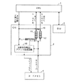
例えば図16に示すような、命令フェッチおよび命令デコードを実行する第1ステージST0、アドレス生成およびメモリリードを実行する第2ステージST1、演算実行およびメモリライトを実行する第3ステージST3を有する3段階のステージからなるパイプライン処理ステージを考える。そして、このようなパイプライン処理ステージにおいて、条件フラグを書き換える演算命令(cmp)の直後に条件分岐命令(cbr)処理が行われるとする。図16から判るように、パイプライン処理では、第3ステージにおいて、cmp実行後に条件分岐命令(cbr)の条件判定を行ってから分岐先あるいは非分岐先の命令がフェッチされるため、2サイクル分の空きスロット(遅延スロット)が生じることになる。
【0005】
そこで、このような場合、遅延分岐方式を利用すると、図16の場合では、条件が不成立の場合は遅延スロットにcbrの次命令を投入し、条件が成立の場合は遅延スロットにcbrの分岐先の命令を投入することができれば、性能向上が最大となる。
【0006】
しかし、このような遅延分岐方式を採用するためには、分岐予測回路を内蔵して、cbrをデコードした時に分岐条件不成立が予測されたときは遅延スロットにcbrの次命令を投入し、分岐条件成立が予測されたときは遅延スロットにcbrの分岐先の命令を投入するようにすればよい。
【0007】
このような分岐予測方式としては、これまでの分岐実行実績に基づき、分岐/否分岐を予測し、分岐/否分岐の判定の結果が判明する前に分岐処理または非分岐処理を進めている。より具体的には、例えば、過去に実行した分岐命令について、当該分岐命令の存在するアドレスと分岐先アドレスとを対にして記憶する履歴テーブルをマイクロプロセッサ内に備えておき、再びこの条件分岐命令を実行する際には、前記履歴テーブルに記憶しておいた分岐先アドレスを用いることで、分岐判定における分岐先アドレスの計算終了前に、当該分岐命令を実行している(例えば、特許文献2,特許文献3参照)。
【0008】
【特許文献1】
特開平4−127237号公報
【特許文献2】
特開平1−239638号公報
【特許文献3】
特開平4−112327号公報
【0009】
【発明が解決しようとする課題】
しかしながら、上記のような分岐予測方式は、予測テーブルの大きさ、応用によって異なるが、ヒット率を90〜95%ぐらいにするには、4Kビット程度の予測テーブルが必要であり、回路が大規模になり、マイクロコンピュータのチップ面積の増大を招くという問題があった。また、リアルタイム性が要求される機器制御用の組み込み用途では、最悪性能の見積もりが重要視されるので、プログラムの実行履歴によって性能が変動しやすい分岐予測回路の内蔵化は、ユーザに敬遠される傾向がある。
【0010】
この発明は上記に鑑みてなされたもので、分岐予測回路を内蔵することなくパイプラインステージの遅延スロットを有効に活用することで、CPU性能を向上し得るマイクロプロセッサを得ることを目的とする。
【0011】
【課題を解決するための手段】
上記目的を達成するため、この発明にかかるマイクロプロセッサは、複数ステージのパイプライン処理を実行するマイクロプロセッサにおいて、命令を記憶するメモリと、一方に前記メモリからプリフェッチされた命令のうちの非分岐命令が格納され、他方に前記プリフェッチされた命令のうちの分岐命令からの分岐先以降にある分岐先命令が格納される2系統のキューバッファと、パイプライン処理を実行する複数の処理ステージを有し、最終段の処理ステージ以外の処理ステージが2系統形成されているパイプライン処理ステージと、前記パイプライン処理ステージの最終段の処理ステージにおいて、分岐命令の条件が成立したか否かを判定し、この判定結果に基づき前記2系統形成されている処理ステージの何れかを最終段の処理ステージに投入する切り替えを行う第1の切り替え手段と、前記判定結果に基づいて前記2系統のキューバッファから前記パイプライン処理ステージの2系統の処理ステージへの接続を切り替える第2の切り替え手段とを備えることを特徴とする。
【0012】
この発明によれば、一方にプリフェッチされた非分岐命令が格納され、他方にプリフェッチされた分岐先命令が格納される2系統のキューバッファと、パイプライン処理を実行する複数の処理ステージを有し、最終段の処理ステージ以外の処理ステージが2系統形成されているパイプライン処理ステージとを備え、2系統形成されているパイプラインの処理ステージに、非分岐命令および分岐先命令を夫々投入して、分岐命令の条件が成立したか否かの判定信号に基づき2系統形成されている処理ステージの何れかを最終段の処理ステージに投入する切り替え制御を行うようにしたので、分岐予測回路を内蔵することなくパイプラインステージの遅延スロットを有効に活用し、CPU性能を向上させることができる。
【0013】
【発明の実施の形態】
以下に添付図面を参照して、この発明にかかるマイクロプロセッサの好適な実施の形態を詳細に説明する。
【0014】
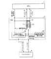
実施の形態1.
図1は本発明の実施の形態1を示すマイクロプロセッサの概略図であり、図2は図1のCPUの内部構成を示す図である。
【0015】
図1に示すマイクロプロセッサは、中央処理装置(CPU)1と、命令用のキャッシュ領域(バスインターフェース回路)としてのコードインターフェース回路(CIU)2、データ用のキャッシュ領域(バスインターフェース回路)としてのデータインターフエース回路(DIU)3および実行するプログラムの命令列が記憶されている主記憶などのコードメモリ4を備えている。CIU2はアドレスバスおよび命令コード用のコードバスを介してコードメモリ4に接続されている。CPU1とCIU2とはオペコードバスA,Bを介して接続されている。なお、図1では、バスインターフェースユニットをCIUとDIUに分離したハーバードアーキテクチャの構成をとっているが、命令とデータの区別をせずに、同一のキャッシュメモリ領域でデータを管理するユニファイドキャッシュ方式を採用するようにしてもよい。
【0016】
CIU2は、分岐命令生成/アドレス生成回路10と、2系統のキューバッファ11,12と、2系統のキューバッファ11,12の2出力とオペコードバスA,Bとの間の切り替えを行う切り替えスイッチ13とを備えている。
【0017】
キューバッファ11,12は、それぞれコードメモリ4からコードバスを介してプリフェッチ(先取り)した命令(コード)を複数個記憶することができるバッファであり、図示しない入力ポインタおよび出力ポインタによってコードメモリ4からプリフェッチした命令のキューバッファ11,12に対する書き込み制御およびキューバッファ11,12に格納された命令の読み出し制御を実行する。
【0018】
分岐命令生成/アドレス生成回路10は、コードバス上に条件分岐命令があるか否かを検出し、分岐命令がないときは図示しないプログラムカウンタの値を随時インクリメントしてアドレスを生成し、分岐命令を検出した場合は分岐命令をデコードし、その情報から分岐命令の分岐先アドレスを生成し、これらの生成したアドレスをアドレスバスを介してコードメモリ4に出力する。また、分岐命令生成/アドレス生成回路10は、CPU1から入力される切り替え信号Saと分岐命令検出信号Sc(図示せず;コードバス上での条件分岐命令を検出する信号)とに基づき2系統のキューバッファ11,12の入力側の選択切り替えを行うためのキュー選択信号Sbを形成し、形成したキュー選択信号Sbをキューバッファ11,12に出力する。キュー選択信号Sbの状態に応じて、コードバスからの命令が2系統のキューバッファ11,12の何れに入力されるかが決定される。
【0019】
また、キューバッファ11,12の出力は切り替えスイッチ13を経由して、オペコードバスA,Bに接続されている。切り替えスイッチ13にはCPU1からの切り替え信号Saが入力されており、切り替えスイッチ13は切り替え信号Saに基づいて、キューバッファ11,12の出力を夫々オペコードバスA,Bに接続する状態と、キューバッファ11,12の出力を夫々オペコードバスB,Aに接続する状態とに切り替える。
【0020】
CPU1からの切り替え信号Saは、後で詳述するが、CPU1が条件分岐命令の分岐の条件が成立したと判断する度に、“High”から“Low”にあるいは“Low”から“High”に切り替えられるものである。したがって、切り替えスイッチ13は、CPU1が条件分岐命令の分岐の条件が成立したと判断する度に、オペコードバスA,Bに対するキューバッファ11,12の接続が逆になる。また、キュー選択信号Sbは、前述したように、コードバス上のデータをキューバッファ11,12のどちらに書き込むかを選択するための信号であり、切り替え信号Saおよび分岐命令検出信号Scの状態に応じて、コードバス上に出力された分岐先のコードあるいはシーケンシャルな動作に従うコードをキューバッファ11,12のどちらに書き込むかが決定される。
【0021】
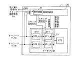
つぎに、CPU1は、図2に示すように、制御回路部20とデータパス部30から構成されている。データパス部30には、パイプライン処理を実行するための複数段の処理ステージを有している。この場合は、3ステージ(ST0,ST1,ST2)でパイプライン処理を実行するものとする。第1ステージST0では、命令フェッチおよび命令デコードを実行し、第2ステージST1では、アドレス生成およびメモリリードを実行し、第3ステージST3では、演算実行およびメモリライトを実行する。
【0022】
ここで、複数ステージ中の最終ステージ(この場合は第3ステージST3)を除く他のステージ(この場合は第1および第2ステージST0,ST1)には、分岐条件が不成立の場合の通常のシーケンシャルな順序の命令に関わる処理を実行するためのシーケンシャル用第1および第2ステージST0_A、ST1_Aと、分岐先の命令に関わる処理を実行するための分岐先用第1および第2ステージST0_B、ST1_Bを有している。第2ステージST1と第3ステージST2との間には、セレクタ31が配され、このセレクタ31によってシーケンシャル用第2ステージST1_Aおよび分岐先用第2ステージST1_Bの何れを選択して第3ステージST2に出力するかが選択される。セレクタ31は制御回路部20からの分岐/非分岐判定信号Sdによってその選択動作を実行する。シーケンシャル用第1ステージST0_AはオペコードバスAに接続され、分岐先用第1ステージST0_BはオペコードバスBに接続されている。
【0023】
データパス部30の制御は制御回路部20から入力される制御信号に従って行われる。そのうちの分岐/非分岐判定信号Sdが第2ステージST1から第3ステージST2へのデータパスをST1_AとST1_Bのどちらを使用するかを選択する。
【0024】
つぎに、CIU2とコードメモリ4との間の動作を図3のタイムチャートを用いて説明する。ここではシーケンシャルな動作に従うコードをキューバッファ11に格納し、分岐時の分岐先のコードをキューバッファ12に格納するものとする。また、コードメモリ4ヘのアクセスはクロック同期で行われ、アクセスサイクル数は1サイクルとする。
【0025】
cycle1〜cycle3ではシーケンシャル動作に従うコード先取り動作をしている。分岐命令検出信号Scが“Low”の時はアドレスバスはプログラムカウンタの値から順次インクリメントされた値となる。また、キュー選択信号Sbが“Low”の時はコードバスのデータはキューバッファ11に書き込まれる。
【0026】
ここでcycle3でコードバス上に分岐命令がのっているとする。このとき分岐命令生成/アドレス生成回路10がそれを検出し、分岐先アドレスを算出する。次のサイクル(cycle4)で分岐命令検出回路Aは分岐先のアドレスを出力する。また、同サイクル(cycle4)で分岐命令生成/アドレス生成回路10はキュー選択信号Sbを“High”にアサートする。この結果、コードバス上の分岐先のコードはキューバッファ12に取り込まれる。cycle5以降は、シーケンシャルな動作に従うコード先取り動作に戻る。なお、分岐先命令(分岐先のコードおよび分岐先のコードに続く命令)はこの後、キューバッファ12に書き込まれていくが、その後分岐先のコードに続く命令中に再度分岐命令が存在している場合は、この分岐命令からの分岐先命令はキューバッファ11に書き込まれていく。
【0027】
なお、1サイクル期間に、キューバッファ11または12に取り込まれるコード長は、1命令に対応する長さにしてもよいし、複数の命令に対応する長さにしてもよい。取り込まれるコード長を1命令に対応する長さとした場合は、分岐先のコードを取り込む際に、複数のサイクルに亘って分岐先以降のコードを取り込む必要がある。
【0028】
以上のような構成にすれば、CPU1で条件分岐命令を実行する前に分岐先の命令を先取りすることが可能となる。
【0029】
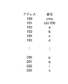
次にCPUの動作を図1〜図3の他に、図4〜図6を用いて説明する。図4は、条件フラグを書き換える演算命令(cmp)の直後に条件分岐命令(cbr)がある場合のアセンブラ言語レベルでのプログラムの一例を示した図であり、アドレス100には条件フラグを書き換える演算命令cmpが、アドレス101には条件分岐命令cbr200(条件が成立した時アドレス200に分岐)が記述されている。更にアドレス102には命令aが、アドレス103には命令bが、アドレス104には命令cが、アドレス105には命令dが、アドレス200には命令pが、命令201には命令qが、命令202には命令rが、命令203には命令sが記述されている。
【0030】
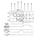
図5は、図4のプログラムを実行したときの、条件分岐命令(cbr)の分岐条件が成立した場合のパイプライン動作と、分岐/非分岐判定信号SdとCIU2へ出力する切り替え信号Saの変化タイミングを示した図である。
【0031】
以下、図1〜図5を参照して分岐条件が成立した場合の具体的動作について説明する。
【0032】
最初の状態では、切り替え信号Saおよび分岐/非分岐判定信号は“Low”である。したがって、キューバッファ11がオペコードバスAに接続されるとともにキューバッファ12がオペコードバスBに接続され、さらにセレクタ31はオペコードA側のST1_Aを選択して第3ステージST2に出力している。
【0033】
まず、第1サイクルで、CIU2が命令cmpを図1のオペコードバスAに供給すると、CPU1は命令cmpをシーケンシャル用第1ステージST0_Aに投入する。第2サイクルで、CIU2が命令cbr200をオペコードバスAに供給すると、cbr200はシーケンシャル用第1ステージST0_Aに投入される。cbr200は分岐命令であるので、それ以前のサイクルでCIU2のキューバッファ12には分岐先のコードが取り込まれている。したがって、オペコードバスBには分岐先のコード(命令p,命令q,命令r,…)が供給されている。
【0034】
第3サイクルで、CPU1はオペコードバスA上に出力されている非分岐先命令aをシーケンシャル用第1ステージST0_Aに投入するとともに、オペコードバスB上に出力されている分岐先命令pを分岐先用第1ステージST0_Bに投入する。さらに第4サイクルでは、CPU1はオペコードバスA上に出力されている非分岐先命令bをシーケンシャル用第1ステージST0_Aに投入するとともに、オペコードバスB上に出力されている分岐先命令qを分岐先用第1ステージST0_Bに投入する。
【0035】
次に、第4サイクルにおいて、cbr200命令の実行ステージST2で、CPU1の制御回路部20が分岐命令の条件成立と判定すると、これに応答してCPU1の制御回路部20は次のサイクル(この場合は第5サイクル)で切り替え信号Saおよび分岐/非分岐判定信号Sdを“High”にアサートする。なお、この場合、分岐/非分岐判定信号Sdは、データパス部30の処理ステージ数(この場合は3ステージ)から1を引いた数(3−1)に対応するサイクル期間(この場合は2)だけ“High”に立ち上がり、その後“Low”に戻るようにする。一方、切り替え信号Saは次の分岐命令の条件成立を判定するまで、“High”を維持している。
【0036】
したがって、第5および第6サイクルでは、セレクタ31は分岐先用第2ステージST1_Bを選択して第3ステージST2に出力する。このため、第5サイクルでは命令pが第3ステージST2へ投入され、また第6サイクルでは命令qが第3ステージST2へ投入される。
【0037】
一方、CIU2に入力される切り替え信号Saが“High”となった時点で、切り替えスイッチ13は逆側に切り替わる。すなわち、切り替えスイッチ13は、切り替え信号Saが“High”となった以降は、キューバッファ12に格納されていた分岐先側の命令(r,s,…)をオペコードバスAに出力し、キューバッファ11に格納されていた非分岐命令をオペコードバスBに出力するようにその接続を切り替える。したがって、第5サイクルで、CIU2が命令rをオペコードバスAに供給すると、CPU1は命令rをシーケンシャル用第1ステージST0_Aに投入する。第6サイクルで、CIU2が命令sをオペコードバスAに供給すると、CPU1は命令sをシーケンシャル用第1ステージST0_Aに投入する。
【0038】
また、前述したように、第7サイクル以降は、分岐/非分岐判定信号Sdは“Low”に切り替わるので、セレクタ31はシーケンシャル用第2ステージST1_Aを選択して第3ステージST2に出力する。このため、第7サイクルでは命令rが第3ステージST2へ投入され、また第8サイクルでは命令sが第3ステージST2へ投入されることになる。
【0039】
図6は、図4のプログラムを実行したときの、条件分岐命令(cbr)の分岐条件が成立しなかった場合のパイプライン動作と、分岐/非分岐判定信号SdとCIU2へ出力する切り替え信号Saの変化タイミングを示した図である。
【0040】
以下、図1〜図4、図6を参照して分岐条件が成立しない場合の具体的動作について説明する。
【0041】
最初の状態では、切り替え信号Saおよび分岐/非分岐判定信号は“Low”である。したがって、キューバッファ11がオペコードバスAに接続されるとともにキューバッファ12がオペコードバスBに接続され、さらにセレクタ31はオペコードA側のST1_Aを選択して第3ステージST2に出力している。
【0042】
まず、第1サイクルで、CIU2が命令cmpをオペコードバスAに供給すると、CPU1は命令cmpをシーケンシャル用第1ステージST0_Aに投入する。第2サイクルで、CIU2が命令cbr200をオペコードバスAに供給すると、cbr200はシーケンシャル用第1ステージST0_Aに投入される。cbr200は分岐命令であるので、それ以前のサイクルでCIU2のキューバッファ12には分岐先のコードが取り込まれている。したがって、オペコードバスBには分岐先のコード(命令p,命令q,命令r,…)が供給されている。
【0043】
第3サイクルで、CPU1はオペコードバスA上に出力されている非分岐先命令aをシーケンシャル用第1ステージST0_Aに投入するとともに、オペコードバスB上に出力されている分岐先命令pを分岐先用第1ステージST0_Bに投入する。さらに第4サイクルでは、CPU1はオペコードバスA上に出力されている非分岐先命令bをシーケンシャル用第1ステージST0_Aに投入するとともに、オペコードバスB上に出力されている分岐先命令qを分岐先用第1ステージST0_Bに投入する。
【0044】
次に、第4サイクルにおいて、cbr200命令の実行ステージST2で、CPU1の制御回路部20が分岐命令の条件が不成立と判定したとする。このため、CPU1の制御回路部20から出力される切り替え信号Saおよび分岐/非分岐判定信号Sdは“Low”のままである。
【0045】
したがって、第5サイクル以降において、セレクタ31はシーケンシャル用第2ステージST1_Aを選択して第3ステージST2に出力する。このため、第5サイクルでは命令aが第3ステージST2へ投入され、また第6サイクルでは命令bが第3ステージST2へ投入される。
【0046】
一方、第5サイクル以降も切り替え信号Saは“Low”のままであるので、以前と同様、キューバッファ11がオペコードバスAに接続されるとともにキューバッファ12がオペコードバスBに接続される。したがって、第5サイクルで、CIU2が命令cをオペコードバスAに供給すると、CPU1は命令cをシーケンシャル用第1ステージST0_Aに投入する。第6サイクルで、CIU2が命令dをオペコードバスAに供給すると、CPU1は命令dをシーケンシャル用第1ステージST0_Aに投入する。
【0047】
また、第7サイクル以降も分岐/非分岐判定信号Sdは“Low”のままであるので、セレクタ31はシーケンシャル用第2ステージST1_Aを選択して第3ステージST2に出力する。このため、第7サイクルでは命令cが第3ステージST2へ投入され、また第8サイクルでは命令dが第3ステージST2へ投入されることになる。
【0048】
このように実施の形態1においては、一方にプリフェッチされた非分岐命令が格納され、他方にプリフェッチされた分岐先命令が格納される2系統のキューバッファ11,12と、パイプライン処理を実行する複数の処理ステージを有し、最終段の処理ステージ以外の処理ステージが2系統形成されているパイプライン処理ステージ(データパス部30)とを備え、2系統形成されているパイプラインの処理ステージに、非分岐命令および分岐先命令を夫々投入して、分岐命令の条件が成立したか否かの判定信号に基づき2系統形成されている処理ステージの何れかを最終段の処理ステージに投入する切り替え制御を行うようにしたので、分岐予測回路を内蔵することなくパイプラインステージの遅延スロットを有効に活用し、CPU性能を向上させることができる。
【0049】
実施の形態2.
つぎに、図7および図8を用いてこの発明の実施の形態2について説明する。図7は実施の形態2に関わるマイクロプロセッサの概略図である。図7に示す実施の形態2においては、各キューバッファ11,12が空か否かを夫々判定するエンプティ判定回路14a,14bをCIU2内に追加するようにしている。エンプティ判定回路14aはキューバッファ11が空になるとアサートされるエンプティ信号EPaをCPU1の制御回路部20に出力する。エンプティ判定回路14bはキューバッファ12が空になるとアサートされるエンプティ信号EPbをCPU1の制御回路部20に出力する。
【0050】
つぎに図7および図8を参照して、遅延スロット投入時に非分岐先のコードがキューバッファ11に蓄積されていない場合で、分岐条件が成立する場合の動作について説明する。プログラムは先の図4に示すものであるとする。
【0051】
命令cbr200が投入されるところ(第2ステージ)までは、図5に示したものと同じ動作であるので説明は省略する。
【0052】
cbr200は分岐命令であるので、第3サイクルで、CPU1はオペコードバスA上に出力されているはずである非分岐先命令aおよびオペコードバスB上に出力されているはずである分岐先命令pを夫々シーケンシャル用第1ステージST0_Aおよび分岐先用第1ステージST0_Bに投入しようとするが、この場合は、第3サイクルにおいてエンプティ信号EPaが“High”にアサートされているので、シーケンシャル用第1ステージST0_Aには何も投入されず、分岐先命令pのみが分岐先用第1ステージST0_Bに投入される。
【0053】
第4サイクルでは、キューバッファ11に非分岐先命令aが格納されたため、エンプティ信号EPaが“Low”にネゲートされる。CIU2は、オペコードバスAに非分岐先命令aを、オペコードバスBに分岐先命令qを供給し、CPU1はそれらの命令をシーケンシャル用第1ステージST0_Aおよび分岐先用第1ステージST0_Bに投入する。
【0054】
さらに、第4サイクルにおいて、cbr200命令の実行ステージST2で、CPU1の制御回路部20が分岐命令の条件成立と判定すると、これに応答してCPU1の制御回路部20は次のサイクル(この場合は第5サイクル)で切り替え信号Saおよび分岐/非分岐判定信号Sdを“High”にアサートする。
【0055】
したがって、第5および第6サイクルでは、セレクタ31は分岐先用第2ステージST1_Bを選択して第3ステージST2に出力する。このため、第5サイクルでは命令pが第3ステージST2へ投入され、また第6サイクルでは命令qが第3ステージST2へ投入される。
【0056】
一方、CIU2に入力される切り替え信号Saが“High”となった時点で、切り替えスイッチ13は逆側に切り替わる。すなわち、切り替えスイッチ13は、切り替え信号Saが“High”となった以降は、キューバッファ12に格納されていた分岐先側の命令(r,s,…)をオペコードバスAに出力し、キューバッファ11に格納されていた非分岐命令をオペコードバスBに出力するようにその接続を切り替える。したがって、第5サイクルで、CIU2が命令rをオペコードバスAに供給すると、CPU1は命令rをシーケンシャル用第1ステージST0_Aに投入する。第6サイクルで、CIU2が命令sをオペコードバスAに供給すると、CPU1は命令sをシーケンシャル用第1ステージST0_Aに投入する。
【0057】
また、前述したように、第7サイクル以降は、分岐/非分岐判定信号Sdは“Low”に切り替わるので、セレクタ31はシーケンシャル用第2ステージST1_Aを選択して第3ステージST2に出力する。このため、第7サイクルでは命令rが第3ステージST2へ投入され、また第8サイクルでは命令sが第3ステージST2へ投入されることになる。
【0058】
このようにこの実施の形態2によれば、CIU2からCPU1にキューバッファ11,12が空であることを示すエンプティ信号EPa,EPbを入力するようにしたので、パイプライン処理の際に、分岐先のコードおよび非分岐先のコードの両方が揃っていなくても両方のコードが揃うまで処理をとめる必要がなくなり、独立にスキップ投入可能となるので、CPU性能を向上させることができる。
【0059】
実施の形態3.
つぎに、図9〜図11を用いてこの発明の実施の形態3について説明する。図9は実施の形態3に関わるマイクロプロセッサの概略図、図10は実施の形態3に関わるCPUの概略図である。
【0060】
この実施の形態3においては、遅延スロットに投入する分岐先命令と非分岐先命令に同じデータ領域からデータを読み出すなどのデータ資源の競合関係が発生しているか否かをCPU1が判定し、競合関係が発生している場合、分岐先命令および非分岐先命令のうちの一方を選択するようにしている。
【0061】
この実施の形態3のマイクロプロセッサにおいては、図9に示すように、DIU3を介してレジスタ値が設定されるレジスタ15が追加されている。レジスタ15のレジスタ値はソフトウェアによって書き換え可能であり、その出力がスキップ選択信号SeとしてCPU1に入力されている。CPU1はDIU3を介してレジスタ15の値すなわちスキップ選択信号Seを書き込み/読み出しすることができる。
【0062】
また、図10に示すように、CPU1の制御回路部20には、調停回路21が追加されている。調停回路21は、遅延スロットに投入する分岐先命令と非分岐先命令に競合関係が発生したか否かを判定し、競合関係が発生している場合は、入力されたスキップ選択信号Seに基づいてスキップ信号SPa,SPbの何れかをアサートする。スキップ信号SPaがアサートされた場合は、シーケンシャル用第2ステージST0_Aでの処理がスキップされ、またスキップ信号SPbがアサートされた場合は、分岐先用第2ステージST0_Bでの処理がスキップされる。すなわち、この場合は、アドレス生成およびメモリリードを実行する第2ステージST1において、上記の競合関係が発生すると、各処理を同時に実行することができないので、一方の処理をスキップさせる。また、例えば、スキップ選択信号Seが“Low”のときはスキップ信号SPaがアサートされて非分岐先命令がスキップされ、スキップ選択信号Seが“High”のときはスキップ信号SPbがアサートされて分岐先命令がスキップされる。
【0063】
つぎに図11を参照して、遅延スロットに投入する分岐先命令と非分岐先命令に競合関係が発生した場合であって、分岐条件が成立する場合の動作について説明する。プログラムは先の図4に示すものであるとする。
【0064】
図11において、最初の遅延スロットに分岐先命令および非分岐先命令が投入されるところ(第2サイクル)までは、先の実施の形態1,2の動作と同じ動作であるので説明は省略する。
【0065】
第3サイクルにおいて、非分岐先命令aおよび分岐先命令pがシーケンシャル用第1ステージST0_Aおよび分岐先用第1ステージST0_Bに2に投入されると、CPU1の制御回路部20は両命令が競合しているか否かを判定する。そして、競合関係があれば、スキップ選択信号Seを参照し、このスキップ選択信号Seに基づいて一方の命令の第2ステージでの処理をスキップさせる。この場合は、スキップ選択信号Seが“Low”であるので、スキップ信号SPaを“High”にアサートする。この結果、第4サイクルにおいて、非分岐先命令aの第2ステージST1_Aでの処理がスキップされる。
【0066】
また、第4サイクルにおいて、非分岐先命令aおよび分岐先命令qとの競合関係が判定されるが、この場合は競合は発生していないとしているので、第5サイクルにおいて、これら非分岐先命令aおよび分岐先命令qについての第2ステージでの処理は、スキップされることなく実行される。それ以外の動作は、図5に示したものと同じであるので、ここではその説明を省略する。
【0067】
このようにこの実施の形態3によれば、遅延スロット投入時に、競合関係があっても分岐先あるいは非分岐先の命令のうちの何れかの処理をスキップしてどちらかの命令を遅延スロットに投入できるので、CPU性能が向上する。また、ソフトウェアでスキップ対象を制御することができるので、予め条件分岐命令の分岐条件成立が発生する頻度がわかる場合は、頻度が高いほうを優先する(頻度が低いほうをスキップ対象にする)ようにプログラミングすれはプログラム全体の実行時間を短縮することができる。
【0068】
実施の形態4.
つぎに、図12を用いてこの発明の実施の形態4について説明する。図12は実施の形態4に関わるマイクロプロセッサの概略図である。
【0069】
この実施の形態4においては、マイクロプロセッサをシステムLSIに搭載し、スキップ選択信号Seをマイクロプロセッサの外部のハードウェア16からマイクロプロセッサのCPU1に入力するようにしている。他は、実施の形態3と同じである。
【0070】
図12のようにマイクロプロセッサを内蔵した組み込み用途のシステムLSIにおいては、条件分岐命令の分岐条件成立の成否を決定する信号がマイクロプロセッサの外部のハードウェア16に存在する場合がある。このような場合は、図9のレジスタ15の代わりに、このハードウェア16からスキップ選択信号Seとして、CPU1に入力することで、実施の形態3と同様の効果を得ることができる。
【0071】
実施の形態5.
つぎに、図13および図14を用いてこの発明の実施の形態5について説明する。図13は実施の形態5に関わるマイクロプロセッサの概略図である。
【0072】
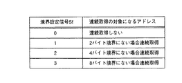
この実施の形態5のマイクロプロセッサにおいては、図13に示すように、CPU1によってDIU3を介してレジスタ値が設定されるレジスタ18が追加されている。レジスタ18のレジスタ値はソフトウェアによって書き換え可能であり、その出力が境界設定信号SfとしてCIU2に入力されている。CPU1はDIU3を介してレジスタ18の値すなわち境界設定信号Sfを書き込み/読み出しすることができる。
【0073】
レジスタ18には、例えば、図14に示すような2ビットの境界設定信号Sfが設定されている。境界設定信号Sfは、分岐命令検出/アドレス生成回路40がコードメモリ4にアクセスして命令コードを読み出す際に、連続アクセスして命令コードを読み出すか否かを指定するための信号である。例えば、分岐命令検出/アドレス生成回路40での1回の読み出しが1バイト単位であるときに、分岐先命令の命令長(コード長)が2バイトである時などに、連続アクセスを行わせるための信号である。
【0074】
図14の場合は、境界設定信号Sfが0のときは連続アクセスは行わない。また、境界設定信号Sfが1のときは、分岐先コードが2バイト境界にないときに連続アクセスを実行させる。境界設定信号Sfが2のときは、分岐先コードが4バイト境界にないときに連続アクセスを実行させる。境界設定信号Sfが3のときは、分岐先コードが8バイト境界にないときに連続アクセスを実行させる。
【0075】
分岐命令検出/アドレス生成回路40は、新たにコードバス上に分岐命令があるのを検出したときに分岐先のアドレスを生成するが、このとき境界設定信号Sfの値と生成した分岐先アドレスの値に基づき、分岐先のコード先取りを連続して行うか否かを判定する機能を有している。そして、この判定結果に応じて分岐先のコード先取りを連続では実行しなかったり、連続して行うようにする。
【0076】
このようにこの実施の形態5によれば、境界設定信号Sfの値と生成した分岐先アドレスの値に基づき、分岐先のコード先取りを連続して行うか否かを判定するようにしているので、分岐先の1回のコード先取りで取得したデータでは分岐先命令として成り立たない場合(例えば、命令長が長い場合)でも、あらかじめ分岐先のコードを余分に先取りできるため、実際に命令がパイプライン処理ステージに投入されるなどの際に、新たに不足分のコードを取得するための待機期間がなくなり、CPU性能が向上する。
【0077】
実施の形態6.
実施の形態6においては、分岐先のコード先取り時にコードを連続して取得するかどうかの情報(連続取得情報)を分岐命令のコードの中に持たせるようにしている。
【0078】
プログラムからコンパイラあるいはアセンブラによってメモリテーブルを作成する際に、分岐先のコードの長さとそのコードがメモリにマッピングされるアドレス情報により、コードを連続取得する必要があるか否かを所定のツールで検出し、その検出情報をもとに各分岐命令内に最適な図14に示すような連続取得情報を夫々設定するようにすれば、プログラム作成時に分岐先のコードの連続取得の可否を意識することなく、実施の形態5と同様の効果が得られる。また、この場合は、実施の形態5に示したレジスタ18は必要なくなる。また、プログラム上でレジスタ18の値を書き換える必要がなくなるので、その分コードメモリ4の低容量化を図ることができる。
【0079】
実施の形態7.
つぎに、図15を用いてこの発明の実施の形態7を説明する。図15は実施の形態5に関わるマイクロプロセッサの概略図である。
【0080】
実施の形態7においては、出現頻度の高い分岐命令に対して、分岐先のコード先取り時にコードを連続して取得するかどうかの情報をコードの中に持たせるようにしている。実施の形態7においては、図15に示すように、CIU2内に連続取得情報検出回路60を追加している。連続取得情報検出回路60は、コードバス上に上述したコード連続取得情報をもたせた分岐命令があるかを検出し、その分岐命令からコード連続取得情報を抽出して、抽出した情報を新たにコード連続取得情報をもたせた分岐命令が検出されるまで保持し、その情報を境界設定信号Sgとして分岐命令検出/アドレス生成回路40に出力する。分岐命令検出/アドレス生成回路40では、先の実施の形態7と同様の動作を実行する。
【0081】
この実施の形態7によれば、全ての分岐命令に連続取得情報をいれる必要がなくなるので、実施の形態5,6の効果に加え、コードメモリ4のメモリ効率が向上するという効果がさらに得られる。
【0082】
実施の形態8.
実施の形態5,6,7において、さらに、分岐先のコード先取りを連続取得するためにコードメモリ4にアクセスする場合のアクセス方式をバーストアクセスになるような回路をCIU2の中に組みこむ。このような構成をとるとコードメモリアクセスに複数サイクル必要な場合、アクセスサイクル数を低減できる場合があるので、プログラム全体の実行時間を短縮することができる。
【0083】
【発明の効果】
以上説明したように、この発明によれば、一方にプリフェッチされた非分岐命令が格納され、他方にプリフェッチされた分岐先命令が格納される2系統のキューバッファと、パイプライン処理を実行する複数の処理ステージを有し、最終段の処理ステージ以外の処理ステージが2系統形成されているパイプライン処理ステージとを備え、2系統形成されているパイプラインの処理ステージに、非分岐命令および分岐先命令を夫々投入して、分岐命令の条件が成立したか否かの判定信号に基づき2系統形成されている処理ステージの何れかを最終段の処理ステージに投入する切り替え制御を行うようにしたので、分岐予測回路を内蔵することなくパイプラインステージの遅延スロットを有効に活用し、CPU性能を向上させることができる。
【図面の簡単な説明】
【図1】この発明の実施の形態1のマイクロプロセッサの構成を示すブロック図である。
【図2】実施の形態1のCPUの内部構成を示すブロック図である。
【図3】CIUとコードメモリとの間の動作を説明するためのタイムチャートである。
【図4】コードメモリに記憶されるプログラムを例示する図である。
【図5】条件分岐命令の分岐条件が成立した場合のパイプライン動作と、分岐/非分岐判定信号Sdおよび切り替え信号Saの変化タイミングを示した図である。
【図6】条件分岐命令の分岐条件が不成立の場合のパイプライン動作と、分岐/非分岐判定信号Sdおよび切り替え信号Saの変化タイミングを示した図である。
【図7】この発明の実施の形態2のマイクロプロセッサの構成を示すブロック図である。
【図8】実施の形態2のマイクロプロセッサの動作を説明するための図である。
【図9】この発明の実施の形態3のマイクロプロセッサの構成を示すブロック図である。
【図10】実施の形態3のCPUの内部構成を示すブロック図である。
【図11】実施の形態3のマイクロプロセッサの動作を説明するための図である。
【図12】この発明の実施の形態4のマイクロプロセッサの構成を示すブロック図である。
【図13】この発明の実施の形態5のマイクロプロセッサの構成を示すブロック図である。
【図14】境界設定信号を説明するための図である。
【図15】この発明の実施の形態7のマイクロプロセッサの構成を示すブロック図である。
【図16】従来技術を示す図である。
【符号の説明】
1 CPU、2 CIU、3 DIU、4 コードメモリ、10,40 分岐命令検出/アドレス生成回路、11,12 キューバッファ、13 切り替えスイッチ、14a,14b エンプティ判定回路、15 レジスタ、16 ハードウェア、18 レジスタ、20 制御回路部、21 調停回路、30 データパス部、31 セレクタ、60 連続取得情報検出回路。[0001]
TECHNICAL FIELD OF THE INVENTION
The present invention relates to a microprocessor having an instruction prefetch (prefetch) function and a pipeline processing function, and more particularly to a microprocessor capable of improving the performance of a CPU by efficiently processing conditional branch instructions.
[0002]
[Prior art]
As a technique for increasing the speed of a microprocessor, there is a so-called pipeline processing method for executing instructions in a pipeline. In such a pipeline processing method, a method called a delayed branch has been conventionally used in order to efficiently process a conditional branch instruction.
[0003]
The conditional branch instruction determines whether or not to branch according to a condition flag or the like in which the execution result of an operation instruction, a transfer instruction, or the like is reflected. In addition, the delayed branch is a method of removing an empty slot by inserting an instruction at an address next to a branch instruction into a delay slot, and using this method is expected to improve the performance of a microprocessor. Such a delayed branch is disclosed in
[0004]
For example, as shown in FIG. 16, three stages including a first stage ST0 for executing instruction fetch and instruction decode, a second stage ST1 for executing address generation and memory read, and a third stage ST3 for executing operation execution and memory write Consider a pipeline processing stage composed of the following stages. Then, in such a pipeline processing stage, it is assumed that the conditional branch instruction (cbr) processing is performed immediately after the operation instruction (cmp) for rewriting the condition flag. As can be seen from FIG. 16, in the pipeline processing, in the third stage, after the cmp is executed, the condition of the conditional branch instruction (cbr) is determined, and then the instruction at the branch destination or the non-branch destination is fetched. Empty slots (delay slots).
[0005]
Therefore, in such a case, when the delay branch method is used, in the case of FIG. 16, if the condition is not satisfied, the instruction following cbr is input to the delay slot, and if the condition is satisfied, the branch destination of cbr is stored in the delay slot. If the instruction can be input, the performance improvement is maximized.
[0006]
However, in order to adopt such a delayed branching method, a branch prediction circuit is built-in, and when a branch condition is not satisfied when cbr is decoded, the next instruction of cbr is input to the delay slot and the branch condition is set. When the establishment is predicted, the instruction of the branch destination of the cbr may be input to the delay slot.
[0007]
As such a branch prediction method, a branch / non-branch is predicted based on a past branch execution result, and branch processing or non-branch processing is advanced before the result of the branch / non-branch determination is found. More specifically, for example, for a branch instruction executed in the past, a history table is stored in the microprocessor in which an address where the branch instruction is present and a branch destination address are stored as a pair, and the conditional branch instruction is stored again. Is executed, the branch instruction is executed before the calculation of the branch destination address in the branch determination is completed by using the branch destination address stored in the history table. And Patent Document 3).
[0008]
[Patent Document 1]
JP-A-4-127237
[Patent Document 2]
JP-A-1-239638
[Patent Document 3]
JP-A-4-112327
[0009]
[Problems to be solved by the invention]
However, the above-described branch prediction method depends on the size and application of the prediction table, but requires a prediction table of about 4 Kbits in order to achieve a hit ratio of about 90 to 95%. Therefore, there is a problem that the chip area of the microcomputer is increased. In addition, in an embedded application for device control that requires real-time performance, estimation of the worst performance is regarded as important, so that the user is not allowed to incorporate a branch prediction circuit whose performance tends to fluctuate depending on the execution history of the program. Tend.
[0010]
The present invention has been made in view of the above, and an object of the present invention is to provide a microprocessor capable of improving CPU performance by effectively utilizing delay slots of a pipeline stage without incorporating a branch prediction circuit.
[0011]
[Means for Solving the Problems]
In order to achieve the above object, a microprocessor according to the present invention is a microprocessor that executes a plurality of stages of pipeline processing, comprising: a memory for storing an instruction; and a non-branch instruction among instructions prefetched from the memory. And two other queue buffers for storing a branch destination instruction following a branch destination from a branch instruction among the prefetched instructions, and a plurality of processing stages for executing pipeline processing. Determining whether a condition of a branch instruction is satisfied in a pipeline processing stage in which two processing stages other than the final processing stage are formed and a final processing stage of the pipeline processing stage; Based on the determination result, one of the processing stages formed in the two systems is set to the final processing stage. First switching means for switching the input to the queue, and second switching means for switching the connection from the two queue buffers to the two processing stages of the pipeline processing stage based on the determination result. It is characterized by having.
[0012]
According to the present invention, there are provided a two-system queue buffer in which one side stores a prefetched non-branch instruction and the other side stores a prefetched branch destination instruction, and a plurality of processing stages for executing pipeline processing. A pipeline processing stage in which two processing stages other than the last processing stage are formed, and a non-branch instruction and a branch destination instruction are respectively input to the processing stages of the pipeline in which two systems are formed. Since the switching control for inputting one of the two processing stages to the final processing stage based on the determination signal as to whether or not the condition of the branch instruction is satisfied is performed, a branch prediction circuit is incorporated. Thus, the delay slot of the pipeline stage can be effectively used, and the CPU performance can be improved.
[0013]
BEST MODE FOR CARRYING OUT THE INVENTION
Preferred embodiments of a microprocessor according to the present invention will be described in detail below with reference to the accompanying drawings.
[0014]
FIG. 1 is a schematic diagram of a microprocessor according to the first embodiment of the present invention, and FIG. 2 is a diagram illustrating an internal configuration of the CPU of FIG.
[0015]
The microprocessor shown in FIG. 1 includes a central processing unit (CPU) 1, a code interface circuit (CIU) 2 as an instruction cache area (bus interface circuit), and data as a data cache area (bus interface circuit). The apparatus includes an interface circuit (DIU) 3 and a
[0016]
The
[0017]
The queue buffers 11 and 12 are buffers capable of storing a plurality of instructions (codes) prefetched (prefetched) from the
[0018]
The branch instruction generation /
[0019]
The outputs of the queue buffers 11 and 12 are connected to opcode buses A and B via a
[0020]
The switching signal Sa from the
[0021]
Next, as shown in FIG. 2, the
[0022]
Here, in the other stages (in this case, the first and second stages ST0 and ST1) except for the final stage (in this case, the third stage ST3) of the plurality of stages, a normal sequential operation is performed when the branch condition is not satisfied. The first and second sequential stages ST0_A and ST1_A for executing processes related to instructions in different orders and the first and second stages ST0_B and ST1_B for branch targets for executing processes related to instructions at branch destinations. Have. A
[0023]
Control of the
[0024]
Next, the operation between the
[0025]
In cycle1 to cycle3, a code prefetch operation according to a sequential operation is performed. When the branch instruction detection signal Sc is “Low”, the address bus has a value sequentially incremented from the value of the program counter. When the queue selection signal Sb is “Low”, data on the code bus is written to the
[0026]
Here, it is assumed that a branch instruction is placed on the code bus in cycle3. At this time, the branch instruction generation /
[0027]
Note that the code length taken into the
[0028]
With such a configuration, it is possible to prefetch a branch destination instruction before the
[0029]
Next, the operation of the CPU will be described with reference to FIGS. 4 to 6 in addition to FIGS. FIG. 4 is a diagram showing an example of a program at an assembler language level in a case where a conditional branch instruction (cbr) is provided immediately after an operation instruction (cmp) for rewriting a condition flag. The instruction cmp describes a conditional branch instruction cbr200 at the address 101 (branch to the
[0030]
FIG. 5 shows the pipeline operation when the branch condition of the conditional branch instruction (cbr) is satisfied when the program of FIG. 4 is executed, and the change of the branch / non-branch determination signal Sd and the switching signal Sa output to the CIU2. FIG. 4 is a diagram showing timing.
[0031]
Hereinafter, a specific operation when the branch condition is satisfied will be described with reference to FIGS.
[0032]
In the initial state, the switching signal Sa and the branch / non-branch determination signal are “Low”. Therefore, the
[0033]
First, in the first cycle, when the
[0034]
In the third cycle, the
[0035]
Next, in the fourth cycle, when the
[0036]
Therefore, in the fifth and sixth cycles, the
[0037]
On the other hand, when the switching signal Sa input to the
[0038]
Further, as described above, the branch / non-branch determination signal Sd switches to “Low” after the seventh cycle, so that the
[0039]
FIG. 6 shows a pipeline operation when the branch condition of the conditional branch instruction (cbr) is not satisfied when the program of FIG. 4 is executed, and a branch / non-branch determination signal Sd and a switching signal Sa output to the CIU2. FIG. 6 is a diagram showing the change timing of the.
[0040]
Hereinafter, a specific operation when the branch condition is not satisfied will be described with reference to FIGS. 1 to 4 and 6.
[0041]
In the initial state, the switching signal Sa and the branch / non-branch determination signal are “Low”. Therefore, the
[0042]
First, in the first cycle, when the
[0043]
In the third cycle, the
[0044]
Next, in the fourth cycle, it is assumed that the
[0045]
Therefore, after the fifth cycle, the
[0046]
On the other hand, since the switching signal Sa remains “Low” even after the fifth cycle, the
[0047]
In addition, since the branch / non-branch determination signal Sd remains “Low” even after the seventh cycle, the
[0048]
As described above, in the first embodiment, two
[0049]
Next, a second embodiment of the present invention will be described with reference to FIGS. FIG. 7 is a schematic diagram of a microprocessor according to the second embodiment. In the second embodiment shown in FIG. 7,
[0050]
Next, with reference to FIG. 7 and FIG. 8, an operation in the case where the code of the non-branch destination is not accumulated in the
[0051]
Until the instruction cbr200 is input (the second stage), the operation is the same as that shown in FIG.
[0052]
Since the
[0053]
In the fourth cycle, since the non-branch destination instruction a is stored in the
[0054]
Further, in the fourth cycle, when the
[0055]
Therefore, in the fifth and sixth cycles, the
[0056]
On the other hand, when the switching signal Sa input to the
[0057]
Further, as described above, the branch / non-branch determination signal Sd switches to “Low” after the seventh cycle, so that the
[0058]
As described above, according to the second embodiment, the empty signals EPa and EPb indicating that the queue buffers 11 and 12 are empty are input from the
[0059]
Next, a third embodiment of the present invention will be described with reference to FIGS. FIG. 9 is a schematic diagram of a microprocessor according to the third embodiment, and FIG. 10 is a schematic diagram of a CPU according to the third embodiment.
[0060]
In the third embodiment, the
[0061]
In the microprocessor according to the third embodiment, as shown in FIG. 9, a
[0062]
As shown in FIG. 10, an
[0063]
Next, with reference to FIG. 11, an operation in a case where a conflict relationship occurs between a branch destination instruction to be inserted into a delay slot and a non-branch destination instruction and a branch condition is satisfied will be described. It is assumed that the program is as shown in FIG.
[0064]
In FIG. 11, the operations up to the point where the branch target instruction and the non-branch target instruction are input to the first delay slot (the second cycle) are the same as the operations in the first and second embodiments, and therefore the description is omitted. .
[0065]
In the third cycle, when the non-branch destination instruction a and the branch destination instruction p are input to the first sequential stage ST0_A and the first stage ST0_B for branch destination, the
[0066]
Further, in the fourth cycle, a conflict relationship between the non-branch destination instruction a and the branch destination instruction q is determined. In this case, since no conflict has occurred, in the fifth cycle these non-branch destination instructions a The processing in the second stage for a and the branch destination instruction q is executed without being skipped. The other operations are the same as those shown in FIG. 5, and the description thereof is omitted here.
[0067]
As described above, according to the third embodiment, when a delay slot is inserted, even if there is a conflicting relationship, the processing of either the branch destination instruction or the non-branch destination instruction is skipped, and either instruction is set to the delay slot. Since it can be inserted, CPU performance is improved. In addition, since the skip target can be controlled by software, if the frequency at which the branch condition of the conditional branch instruction is satisfied is known in advance, the higher frequency is prioritized (the lower frequency is set as the skip target). Programming can reduce the execution time of the entire program.
[0068]
Next, a fourth embodiment of the present invention will be described with reference to FIG. FIG. 12 is a schematic diagram of a microprocessor according to the fourth embodiment.
[0069]
In the fourth embodiment, a microprocessor is mounted on a system LSI, and a skip selection signal Se is input from
[0070]
In a system LSI for embedded use incorporating a microprocessor as shown in FIG. 12, a signal for determining whether or not the branch condition of a conditional branch instruction is satisfied may be present in
[0071]
Embodiment 5 FIG.
Next, a fifth embodiment of the present invention will be described with reference to FIGS. FIG. 13 is a schematic diagram of a microprocessor according to the fifth embodiment.
[0072]
In the microprocessor according to the fifth embodiment, as shown in FIG. 13, a
[0073]
In the
[0074]
In the case of FIG. 14, continuous access is not performed when the boundary setting signal Sf is 0. When the boundary setting signal Sf is 1, continuous access is executed when the branch destination code is not at a 2-byte boundary. When the boundary setting signal Sf is 2, continuous access is executed when the branch destination code is not on a 4-byte boundary. When the boundary setting signal Sf is 3, continuous access is executed when the branch destination code is not at the 8-byte boundary.
[0075]
The branch instruction detection /
[0076]
As described above, according to the fifth embodiment, it is determined whether or not to continuously execute code prefetching of a branch destination based on the value of the boundary setting signal Sf and the generated value of the branch destination address. Even if the data obtained by one code prefetch at the branch destination does not hold as a branch destination instruction (for example, when the instruction length is long), an extra code at the branch destination can be prefetched in advance, so that the instruction is actually pipelined. For example, when the CPU is put into the processing stage, there is no waiting period for acquiring a newly lacking code, and the CPU performance is improved.
[0077]
Embodiment 6 FIG.
In the sixth embodiment, information (continuous acquisition information) as to whether or not to acquire codes continuously at the time of code prefetching of a branch destination is included in the code of the branch instruction.
[0078]
When a memory table is created from a program by a compiler or assembler, a predetermined tool detects whether or not it is necessary to continuously acquire codes based on the length of the code at the branch destination and the address information where the code is mapped to the memory. If the optimum continuous acquisition information as shown in FIG. 14 is set in each branch instruction based on the detection information, it is possible to be conscious of whether or not continuous acquisition of the branch destination code is possible at the time of program creation. Therefore, the same effect as in the fifth embodiment can be obtained. In this case, the
[0079]
Embodiment 7 FIG.
Next, a seventh embodiment of the present invention will be described with reference to FIG. FIG. 15 is a schematic diagram of a microprocessor according to the fifth embodiment.
[0080]
In the seventh embodiment, for a branch instruction having a high appearance frequency, information as to whether or not to acquire the code continuously at the time of prefetching the code of the branch destination is included in the code. In the seventh embodiment, as shown in FIG. 15, a continuous acquisition
[0081]
According to the seventh embodiment, it is not necessary to put continuous acquisition information in all branch instructions. Therefore, in addition to the effects of the fifth and sixth embodiments, the effect that the memory efficiency of the
[0082]
Embodiment 8 FIG.
In the fifth, sixth, and seventh embodiments, a circuit is provided in the
[0083]
【The invention's effect】
As described above, according to the present invention, two queue buffers for storing prefetched non-branch instructions on one side and prefetched branch destination instructions on the other side, and a plurality of queue buffers for executing pipeline processing And a pipeline processing stage in which two processing stages other than the final processing stage are formed. A non-branch instruction and a branch destination Since each instruction is input and one of the two processing stages is input to the final processing stage based on the determination signal as to whether or not the condition of the branch instruction is satisfied, the switching control is performed. The CPU performance can be improved by effectively utilizing the delay slots of the pipeline stage without incorporating a branch prediction circuit.
[Brief description of the drawings]
FIG. 1 is a block diagram illustrating a configuration of a microprocessor according to a first embodiment of the present invention.
FIG. 2 is a block diagram illustrating an internal configuration of a CPU according to the first embodiment;
FIG. 3 is a time chart for explaining an operation between a CIU and a code memory.
FIG. 4 is a diagram illustrating a program stored in a code memory.
FIG. 5 is a diagram illustrating a pipeline operation when a branch condition of a conditional branch instruction is satisfied, and a change timing of a branch / non-branch determination signal Sd and a switching signal Sa.
FIG. 6 is a diagram illustrating a pipeline operation when a branch condition of a conditional branch instruction is not satisfied, and a change timing of a branch / non-branch determination signal Sd and a switching signal Sa.
FIG. 7 is a block diagram showing a configuration of a microprocessor according to a second embodiment of the present invention.
FIG. 8 is a diagram for explaining an operation of the microprocessor according to the second embodiment;
FIG. 9 is a block diagram illustrating a configuration of a microprocessor according to a third embodiment of the present invention.
FIG. 10 is a block diagram showing an internal configuration of a CPU according to a third embodiment.
FIG. 11 is a diagram illustrating an operation of the microprocessor according to the third embodiment.
FIG. 12 is a block diagram illustrating a configuration of a microprocessor according to a fourth embodiment of the present invention.
FIG. 13 is a block diagram showing a configuration of a microprocessor according to a fifth embodiment of the present invention.
FIG. 14 is a diagram for explaining a boundary setting signal.
FIG. 15 is a block diagram showing a configuration of a microprocessor according to a seventh embodiment of the present invention.
FIG. 16 is a diagram showing a conventional technique.
[Explanation of symbols]
1 CPU, 2 CIUs, 3 DIUs, 4 code memories, 10, 40 branch instruction detection / address generation circuits, 11, 12 queue buffers, 13 changeover switches, 14a, 14b empty determination circuits, 15 registers, 16 hardware, 18 registers , 20 control circuit section, 21 arbitration circuit, 30 data path section, 31 selector, 60 continuous acquisition information detection circuit.
Claims (6)
命令を記憶するメモリと、
一方に前記メモリからプリフェッチされた命令のうちの非分岐命令が格納され、他方に前記プリフェッチされた命令のうちの分岐命令からの分岐先以降にある分岐先命令が格納される2系統のキューバッファと、
パイプライン処理を実行する複数の処理ステージを有し、最終段の処理ステージ以外の処理ステージが2系統形成されているパイプライン処理ステージと、
前記パイプライン処理ステージの最終段の処理ステージにおいて、分岐命令の条件が成立したか否かを判定し、この判定結果に基づき前記2系統形成されている処理ステージの何れかを最終段の処理ステージに投入する切り替えを行う第1の切り替え手段と、
前記判定結果に基づいて前記2系統のキューバッファから前記パイプライン処理ステージの2系統の処理ステージへの接続を切り替える第2の切り替え手段と、
を備えることを特徴とするマイクロプロセッサ。In a microprocessor that executes pipeline processing of multiple stages,
A memory for storing instructions;
A two-system queue buffer in which a non-branch instruction of instructions prefetched from the memory is stored on one side and a branch destination instruction following a branch destination from the branch instruction of the prefetched instructions is stored on the other side. When,
A pipeline processing stage having a plurality of processing stages for executing pipeline processing, wherein two processing stages other than the final processing stage are formed;
In the last processing stage of the pipeline processing stage, it is determined whether or not the condition of the branch instruction is satisfied. Based on the determination result, one of the processing stages formed in the two systems is determined as the final processing stage. First switching means for switching the input to
Second switching means for switching a connection from the two queue buffers to the two processing stages of the pipeline processing stage based on the determination result;
A microprocessor comprising:
Priority Applications (2)
| Application Number | Priority Date | Filing Date | Title |
|---|---|---|---|
| JP2002355311A JP2004192021A (en) | 2002-12-06 | 2002-12-06 | Microprocessor |
| US10/445,831 US20040111592A1 (en) | 2002-12-06 | 2003-05-28 | Microprocessor performing pipeline processing of a plurality of stages |
Applications Claiming Priority (1)
| Application Number | Priority Date | Filing Date | Title |
|---|---|---|---|
| JP2002355311A JP2004192021A (en) | 2002-12-06 | 2002-12-06 | Microprocessor |
Publications (1)
| Publication Number | Publication Date |
|---|---|
| JP2004192021A true JP2004192021A (en) | 2004-07-08 |
Family
ID=32463382
Family Applications (1)
| Application Number | Title | Priority Date | Filing Date |
|---|---|---|---|
| JP2002355311A Pending JP2004192021A (en) | 2002-12-06 | 2002-12-06 | Microprocessor |
Country Status (2)
| Country | Link |
|---|---|
| US (1) | US20040111592A1 (en) |
| JP (1) | JP2004192021A (en) |
Families Citing this family (9)
| Publication number | Priority date | Publication date | Assignee | Title |
|---|---|---|---|---|
| JP2006018412A (en) * | 2004-06-30 | 2006-01-19 | Fujitsu Ltd | Address generator and arithmetic circuit |
| TWI328771B (en) * | 2005-07-15 | 2010-08-11 | Nvidia Corp | Pipelined central processing unit structure and method of processing a sequence of instructions |
| TW200849088A (en) * | 2007-06-12 | 2008-12-16 | Holtek Semiconductor Inc | Power-saving data processor |
| CH699208B1 (en) * | 2008-07-25 | 2019-03-29 | Em Microelectronic Marin Sa | Shared memory processor circuit and buffer system. |
| CN105468334A (en) * | 2008-12-25 | 2016-04-06 | 世意法(北京)半导体研发有限责任公司 | Branch decreasing inspection of non-control flow instructions |
| CN106990942A (en) * | 2011-06-29 | 2017-07-28 | 上海芯豪微电子有限公司 | branch processing method and system |
| US9000805B2 (en) * | 2013-01-29 | 2015-04-07 | Broadcom Corporation | Resonant inductor coupling clock distribution |
| US10901743B2 (en) * | 2018-07-19 | 2021-01-26 | International Business Machines Corporation | Speculative execution of both paths of a weakly predicted branch instruction |
| CN111538535B (en) * | 2020-04-28 | 2021-09-21 | 支付宝(杭州)信息技术有限公司 | CPU instruction processing method, controller and central processing unit |
Family Cites Families (6)
| Publication number | Priority date | Publication date | Assignee | Title |
|---|---|---|---|---|
| US4028670A (en) * | 1976-02-06 | 1977-06-07 | International Business Machines Corporation | Fetch instruction for operand address calculation |
| US4532589A (en) * | 1981-12-02 | 1985-07-30 | Hitachi, Ltd. | Digital data processor with two operation units |
| US5511172A (en) * | 1991-11-15 | 1996-04-23 | Matsushita Electric Co. Ind, Ltd. | Speculative execution processor |
| KR100309566B1 (en) * | 1992-04-29 | 2001-12-15 | 리패치 | Method and apparatus for grouping multiple instructions, issuing grouped instructions concurrently, and executing grouped instructions in a pipeline processor |
| US6393527B1 (en) * | 1998-12-18 | 2002-05-21 | Ati International Srl | Prefetch buffer with continue detect |
| US6647487B1 (en) * | 2000-02-18 | 2003-11-11 | Hewlett-Packard Development Company, Lp. | Apparatus and method for shift register rate control of microprocessor instruction prefetches |
-
2002
- 2002-12-06 JP JP2002355311A patent/JP2004192021A/en active Pending
-
2003
- 2003-05-28 US US10/445,831 patent/US20040111592A1/en not_active Abandoned
Also Published As
| Publication number | Publication date |
|---|---|
| US20040111592A1 (en) | 2004-06-10 |
Similar Documents
| Publication | Publication Date | Title |
|---|---|---|
| JP5357017B2 (en) | Fast and inexpensive store-load contention scheduling and transfer mechanism | |
| JP5425627B2 (en) | Method and apparatus for emulating branch prediction behavior of explicit subroutine calls | |
| JP5889986B2 (en) | System and method for selectively committing the results of executed instructions | |
| US5727227A (en) | Interrupt coprocessor configured to process interrupts in a computer system | |
| US6760835B1 (en) | Instruction branch mispredict streaming | |
| US6912650B2 (en) | Pre-prefetching target of following branch instruction based on past history | |
| JP2003196084A (en) | System having read modifying write unit | |
| US20220113966A1 (en) | Variable latency instructions | |
| JP2004192021A (en) | Microprocessor | |
| US20060095746A1 (en) | Branch predictor, processor and branch prediction method | |
| JP2006216040A (en) | Method and apparatus for dynamic prediction by software | |
| JP2006517322A (en) | Method and apparatus for hazard detection and management in pipelined digital processors | |
| US20070079076A1 (en) | Data processing apparatus and data processing method for performing pipeline processing based on RISC architecture | |
| JP5128382B2 (en) | Method and apparatus for executing multiple load instructions | |
| JP2004145454A (en) | Information processor and information processing method | |
| US20080065870A1 (en) | Information processing apparatus | |
| JP2003263313A (en) | Digital processor and method of selecting command | |
| JP3490005B2 (en) | Instruction control apparatus and method | |
| US6769057B2 (en) | System and method for determining operand access to data | |
| WO2020214624A1 (en) | Variable latency instructions | |
| US20040103267A1 (en) | Data processor having cache memory | |
| JP2004062427A (en) | Microprocessor | |
| JP2001022577A (en) | Information processor | |
| US6735686B1 (en) | Data processing device including two instruction decoders for decoding branch instructions | |
| JP2009146227A (en) | Central processing unit, selection circuit, and selecting method |
Legal Events
| Date | Code | Title | Description |
|---|---|---|---|
| A621 | Written request for application examination |
Free format text: JAPANESE INTERMEDIATE CODE: A621 Effective date: 20051102 |
|
| A977 | Report on retrieval |
Free format text: JAPANESE INTERMEDIATE CODE: A971007 Effective date: 20060801 |
|
| A131 | Notification of reasons for refusal |
Free format text: JAPANESE INTERMEDIATE CODE: A131 Effective date: 20060808 |
|
| A02 | Decision of refusal |
Free format text: JAPANESE INTERMEDIATE CODE: A02 Effective date: 20070626 |