JP4194302B2 - Development device and development processing method - Google Patents
Development device and development processing method Download PDFInfo
- Publication number
- JP4194302B2 JP4194302B2 JP2002167565A JP2002167565A JP4194302B2 JP 4194302 B2 JP4194302 B2 JP 4194302B2 JP 2002167565 A JP2002167565 A JP 2002167565A JP 2002167565 A JP2002167565 A JP 2002167565A JP 4194302 B2 JP4194302 B2 JP 4194302B2
- Authority
- JP
- Japan
- Prior art keywords
- substrate
- cleaning liquid
- supply nozzle
- liquid supply
- developer
- Prior art date
- Legal status (The legal status is an assumption and is not a legal conclusion. Google has not performed a legal analysis and makes no representation as to the accuracy of the status listed.)
- Expired - Fee Related
Links
Images


Description
【0001】
【発明の属する技術分野】
本発明は、基板の表面にレジストが塗布されて、露光処理がされた基板に対して、現像液を供給して現像処理を行う現像装置及び現像処理方法に関する。
【0002】
【従来の技術】
半導体ウエハや液晶ディスプレイのLCD基板の表面上に回路パターンを形成するためのマスクは、例えばウエハ表面にフォトレジスト溶液(以下レジストという)の塗布を行い、光等の照射を行った後、前記レジストが例えばネガ形ならば光の当った部分が硬化するので、硬化しない部分即ちレジストの溶けやすい部分を現像液により溶解することにより形成される。また、例えばポジ形レジストであれば露光された部分が現像液で溶解される。
【0003】
例えばネガ型のレジストが現像される様子について説明すると、図16に示すように、先ず露光処理を終えた例えば半導体ウェハ(以下、ウェハという)Wの表面のレジスト10に対して現像液を塗布した後、所定の時間その状態を保持させると、現像液に対して溶解性の部分11が溶解する。続いてウェハWの表面に洗浄液を供給してウェハW上の現像液を洗い流し、乾燥させてレジストパターン12を得る。
【0004】
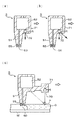
従来の現像装置を用いた現像処理においては、図17(a)に示すように、露光処理されたウエハを略水平姿勢で保持し、かつウェハWを鉛直軸回りに回転可能なスピンチャック13に載置して現像処理が行われる。先ずウェハWの表面全体に現像液Dを塗布し、次いで所定時間例えば60秒程度の静止現像を行って現像反応を進行させる。そして所定の時間が経過すると、図17(b)に示すように、前記ウエハ表面の例えば中心部に対向するようし設定された洗浄液ノズル14から例えば純水等の洗浄液Rを供給すると共に、ウエハWを例えば1000rpm程度の周速度で回転させ、この遠心力の作用によりレジスト溶解成分を含む現像液Dを洗い流して、最後に図17(c)に示すように、ウエハWを高速回転させることにより乾燥させる。
【0005】
【発明が解決しようとしている課題】
しかしながら、近年ウェハWは大型化しており、ウエハWを回転させながら遠心力の作用を利用して現像液Dを洗い流す従来の手法では、ウェハWの周縁部に作用する遠心力と、中心部に作用する遠心力との差が大きくなり、遠心力の弱い中心部においては洗浄が不十分になる場合がある。即ち、例えばレジストパターンの谷間にあるレジストの溶解成分は高濃度になっており、更には一度溶解したレジスト成分が析出したものや未溶解のレジスト粒子等を含んでおり、いわば泥状の状態となっている場合がある。このような溶解生成物は、前記遠心力が小さいと、この遠心力よりも例えばウェハW表面やレジストパターンの壁面との摩擦力が強く作用して、ウェハWを回転しても振り払えずに残ってしまう場合がある。そしてこの溶解生成物がパターン表面(レジスト表面、下地表面)に付着したまま乾燥して現像欠陥となる懸念がある。
【0006】
一方、ウェハWの回転数を増やして中心部の遠心力を大きくする手法が検討されているが、この場合には周縁部の遠心力が強すぎてレジストパターンが剥離してしまったり、あるいは転倒してしまう懸念がある。
【0007】
本発明はこのような事情の下になされたものであり、現像欠陥を低減し、また現像液の洗浄を短時間で行うことのできる技術を提供することにある。
【0008】
【課題を解決するための手段】
本発明の現像装置は、基板の表面にレジストが塗布されて、露光処理がされた基板を現像する現像装置において、
基板を水平に保持する基板保持部と、
この基板保持部に保持された基板の表面に現像液を供給する現像液供給ノズルと、
前記基板の有効領域の幅とほぼ同じかそれ以上の長さに亘って形成された吐出口を有し、現像液が塗布された基板の表面に対して洗浄液を供給するための洗浄液供給ノズルと、
前記吐出口の下端部が現像液の液面よりも下でありかつ基板の表面との離間距離が0.4mm以下の高さ位置で前記洗浄液供給ノズルを、基板の一端側から他端側に亘って移動させる移動機構と、を備えたことを特徴とする。
【0009】
本発明の現像装置によれば、洗浄液供給ノズルの吐出口から吐出された洗浄液が基板の表面に衝突したときに発生する横方向へ押し出しの作用と、洗浄液供給ノズルの側壁面による押し出しの作用とが相俟って、基板表面上のレジスト成分を含む現像液を排出することができる。このため基板の表面に現像液やレジスト成分が残るのを抑えることができるので、現像欠陥の少ないパターンを得ることができる。
【0010】
他の発明の現像装置は、基板の表面にレジストが塗布されて、露光処理がされた基板を現像する現像装置において、
基板を水平に保持する基板保持部と、
この基板保持部に保持された基板の表面に現像液を供給する現像液供給ノズルと、
前記基板の有効領域の幅とほぼ同じかそれ以上の長さに亘って形成された吐出口を有し、現像液が塗布された基板の表面に対して洗浄液を供給するための洗浄液供給ノズルと、
前記洗浄液供給ノズルの進行方向側の側面部に設けられ、前方側に傾斜した気体噴気口と、
前記吐出口の下端部が現像液の液面よりも下になる高さ位置で前記洗浄液供給ノズルを基板の一端側から他端側に亘って移動させる移動機構と、を備えたことを特徴とする。
【0011】
また洗浄液供給ノズルは、例えばその進行方向に複数の吐出口が配列されていてもよく、これら各吐出口には、例えば夫々流量調整部が設けられていてもよい。更には、例えば現像液が塗布された基板を所定の時間回転させた後に、洗浄液を供給するようにしてもよい。更にまた、前記洗浄液供給ノズルの吐出口から洗浄液を吐出しながら基板の一端側から他端側に亘ってを移動させて洗浄を行った後に、例えば基板の中心部に洗浄液を供給しながら基板を回転させる洗浄を行うようにしてもよい。更には、前記気体噴気口は、前記洗浄液供給ノズルの長さ方向に配置され前記基板上に形成された現像液膜に対して所定の 角度で気体を供給するようにしてもよい。
【0012】
本発明の現像処理方法は、基板の表面にレジストが塗布されて露光処理がされた基板を現像する現像処理方法において、
水平に保持された基板の表面に現像液を供給し現像液膜を形成する工程と、
この基板の有効領域の幅と略同じかそれ以上の長さに亘って形成された吐出口を有した洗浄液供給ノズルを当該基板の一端側から他端側に亘って複数回移動させる工程と、
この洗浄液供給ノズルの移動に際し前記基板に向けて洗浄液を供給して洗浄をする工程と、を含み、
前記洗浄液供給ノズルは、吐出口の下端部が前記基板表面上の現像液又は洗浄液に浸漬する高さ位置で移動させることを特徴とする。
【0013】
前記洗浄液供給ノズルから前記基板に向けて洗浄液を供給する工程において、この洗浄液供給ノズルの進行方向側に設けられた気体噴気口から当該基板に向けて気体を噴出するようにしてもよい。また前記気体噴気口は、前記洗浄液供給ノズルの長さ方向に沿って配置されると共に進行方向の前方側に傾斜しており、前記基板に向けて気体を噴出して前記レジストから溶け出した溶解生成物を掃き出すようにしてもよい。
【0014】
他の発明に係る現像処理方法は、基板の表面にレジストが塗布されて露光処理がされた基板を現像する現像処理方法において、
水平に保持された基板の表面に現像液を供給し現像液膜を形成する工程と、
この基板の有効領域の幅と略同じかそれ以上の長さに亘って形成された吐出口の下端部が当該基板表面上の現像液又は洗浄液に浸漬する高さ位置で、洗浄液供給ノズルを基板の一端側から他端側に亘って複数回移動させる工程と、
この洗浄液供給ノズルの移動に際し前記基板に向けて洗浄液を供給して洗浄をする工程と、を含み、
前記複数回の移動において、2回目以降に洗浄液供給ノズルを前記基板の一端側から他端側に亘って移動させるときに当該基板を鉛直軸回りに回転させる工程と、を含むことを特徴とする。ここで、前記洗浄液供給ノズルは、その進行方向に複数の吐出口が配列されていてもよい。また前記基板を鉛直軸回りに回転させる工程において、基板の回転数を変えるようにしてもよい。
【0015】
【発明の実施の形態】
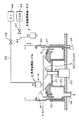
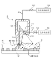
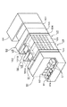
本発明に係る現像装置の第1の実施の形態について説明する。図1は現像装置の概略断面図であり、図2は概略平面図である。図中2は基板である例えば8インチサイズのウエハWの裏面中心部を真空吸着し、略水平に保持するスピンチャックであり、このスピンチャック2は駆動部20により回転および昇降できるように構成されている。ウエハWがスピンチャック2に吸着保持された状態において、ウエハWの側周方を囲むようにして外カップ30と内カップ31とが設けられている。また内カップ31は円筒の上部側が上方内側に傾斜し、上部側開口部が下部側開口部より狭くなるように形成されており、更には外カップ30が昇降部32により上昇すると、外カップ30の移動範囲の一部において連動して昇降するように構成されている。更にスピンチャック2の下方側には、スピンチャック2の回転軸を囲む円板33が設けられており、更には円板33の周り全周に亘って凹部を形成し、底面に排液口34が形成されている液受け部35とが設けられている。また円板33の周縁部には上端がウエハWの裏面に接近する断面山形のリング体36が設けられている。
【0016】
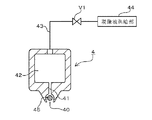
続いてスピンチャック2に吸着保持されたウエハWに現像液を供給(塗布)するための現像供給手段をなす現像液供給ノズル4について説明する。この現像液供給ノズル4は、例えば図1及び図3に示すように、例えばウエハWの有効領域(デバイスの形成領域)の幅と同じかそれ以上の長さに亘る現像液の吐出領域を形成できるように、ノズルの長さ方向に配列された例えばスリット形状の吐出口40と、この吐出口40に現像液流路41を介して連通される現像液貯留部42を備えている。また当該現像液貯留部42は、供給路43例えば配管を介して現像液供給部44と接続されており、その途中には開閉バルブV1が設けられている。なお図中45は吐出口40の内部に配置された例えば石英棒あるいは多孔体をなす緩衝棒であり、この緩衝棒45により流路41からの現像液の吐出圧力が現像液供給ノズル4の長さ方向で均一となり、また吐出口40からの現像液の液漏れが防止されるようになっている。このような現像液供給ノズル4は、図2に示すように、第1の移動機構46により昇降自在であり、更には外カップ30の外側に設けられたガイドレールGに沿って横方向に移動可能に設けられている。なお、現像液供給ノズル4は前記した構成に限られず、例えば単にスリット形状の吐出口40が形成され、緩衝棒45を設けないようにしてもよい。
【0017】
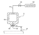
続いてウエハWに洗浄液を供給するための洗浄液供給手段をなす洗浄液供給ノズル5について説明する。この洗浄液供給ノズル5は、図4に示すように、例えばウエハWの有効領域(デバイスの形成領域)の幅と同じかそれ以上の長さに亘る洗浄液の吐出領域を形成できるように、ノズルの長さ方向に配列された例えばスリット形状の吐出口50と、この吐出口50に洗浄液流路51を介して連通される洗浄液貯留部52を備えている。また洗浄液貯留部52は、供給路53例えば配管を介して洗浄液供給部54と接続されており、その途中には開閉バルブV2が設けられている。また55は上述の機能を有する緩衝棒である。
【0018】
この洗浄液供給ノズル5は第2の移動機構56により昇降自在であり、更には待機位置例えばガイドレールGの一端側の位置からウエハWの上方側を通って前記待機位置とウエハWを挟んで対向する位置まで水平移動可能に設けられている。ここで図2において第1の移動機構46及び第2の移動機構56が夫々示されている位置は既述の非作業時における現像液供給ノズル4及び洗浄液供給ノズル5の待機位置であって、ここには例えば上下可動の板状体により構成された第1の移動機構46及び第2の移動機構56の待機部57,58が設けられている。また外カップ30、内カップ31、昇降部32、第1の移動機構46及び第2の移動機構56は箱状の筐体59により囲まれた一ユニットとして形成されており、筐体59内には図示しない搬送口を介して図示しない搬送アームによりウエハWの搬入出がなされる。
【0019】
これまで述べてきた駆動部20、昇降部32、第1の移動機構46及び第2の移動機構56、開閉バルブV1,V2は夫々制御部6と接続されており、例えば駆動部20によるスピンチャック2の昇降に応じて、開閉バルブV1,V2の開閉や、第1の移動機構46による現像液供給ノズル4の移動および第2の移動機構56による洗浄液供給ノズル5の移動を行うように、各部を連動させたコントロールを可能としている。この際前記開閉バルブV1,V2の開閉動作のタイミングや、第1の移動機構46や第2の移動機構56の移動開始や停止のタイミング、移動速度は制御部6により予め設定された処理レシピに基づいて制御されるようになっている。
【0020】
続いて上述の現像装置を用いて現像処理する工程について図5を用いて説明する。先ず外カップ30および内カップ31が共に下降位置に設定された状態にてスピンチャック2を外カップ30の上方まで上昇させ、既に前工程でレジストが塗布されて、露光処理が行われたウエハWが図示しない搬送アームからスピンチャック2に渡される。そしてウエハWが例えば図1中実線で示す所定の位置に来るようにスピンチャック2を下降させる。
【0021】
続いて現像液供給ノズル4が第1の移動機構46により外カップ30とウエハWの周縁との間の吐出開始位置に案内され、次いで吐出口40がウエハW表面レベルよりも例えば1mm程度高い位置に設定される。ここで開閉バルブV1を開いて吐出口40から現像液Dの吐出を開始しながら、図5(a)に示すように、当該現像液供給ノズル4をウエハWの一端側から他端側へ所定の速度例えば65mm/秒程度のスキャン速度で移動させてウェハWの表面に現像液Dを塗布して、膜厚が例えば1mm程度の現像液膜を形成する。続いて図5(b)に示すように、この状態を所定時間例えば60秒程度保持する静止現像を行って現像反応を進行させる。一方、現像液供給ノズル4は、ウエハWの他端側を通過した後、開閉バルブV1を閉じて現像液Dの吐出を停止して待機部57に戻される。
【0022】
続いて洗浄液供給ノズル5が第2の移動機構56により前記吐出開始位置に案内され、次いで洗浄液供給ノズル5が下降して、ノズルの下端部である吐出口50の先端とウエハWの表面との離間距離Lが0.4mm以下例えば0.3mmになるように設定される。なお、ここでいうウェハW表面はレジスト膜の表面を意味するが、本発明が問題にしている現像欠陥が起こるレジスト膜の厚さは通常0.5μm程度であるからレジスト膜の厚さは離間距離Lに比べて十分小さい。そして図5(c)に示すように、開閉バルブV2を開いて吐出口50から洗浄液R例えば純水を例えば2.0リットル/分(流速で0.05m/秒)の流量、例えば1.7kgf/cm2(0.17MPa)の吐出圧で吐出すると共に、洗浄液供給ノズル5を例えば120mm/秒程度のスキャン速度でウエハWの一端側から他端側に亘って移動させる。この操作をスキャン洗浄と呼ぶとすると、その後続けてスキャン洗浄を2回行い、合計3回のスキャン洗浄を行う。この例では8インチサイズのウェハWの一端から他端までスキャンするのに1.7秒程度かかることからスキャン洗浄時間は5.1秒間程度行っていることになる。洗浄液供給ノズル5は開閉バルブV2を閉じて洗浄液Rの吐出を停止して待機部58に戻される。
【0023】
ここでウェハWの表面が洗浄される様子について詳しく説明する。図6に模式的に示すように、洗浄液供給ノズル5がスキャンされる際においては、ウェハW上の現像液Dは、洗浄液供給ノズル5の側壁面により前方側に向かって押されることにより液流れを形成し、この液流れにより前方側のパターンの谷間にあるレジストの溶解生成物(現像パドル)の表層部を掃き出す。そして直ぐ後に通過する洗浄液供給ノズル5の吐出口50から吐出された洗浄液Rが残りの溶解生成物例えばパターンの底部や角部に付着した溶解生成物をその吐出圧により掃き出す。このようにしてパターンの谷間から掃き出された溶解生成物は、ウェハWに供給される洗浄液Rによって希薄化され、後の工程にて洗浄液Rと共にウェハW上から取り除かれることとなる。なお、1回目のスキャン洗浄で溶解生成物の大部分を排除して洗浄し、2回目以降にはウェハWを例えば10〜1000rpmで回転させながらスキャン洗浄を行うようにしてもよく、またスキャン洗浄中に回転数を変化させつつ行ってももちろんよい。
【0024】
説明を図5に戻すと、上述のようにしてウエハWの表面の現像液Dが洗浄液Rで置換された後、昇降部32により外カップ30および内カップ31が上昇位置に設定され、図5(d)に示すように、ウェハWをある程度乾燥させるために例えば4000rpm程度の回転数にてウェハWを回転させて洗浄液Rを振り切るスピン乾燥が行われる。しかる後ウエハWは図示しない搬送アームにより現像装置の外へ搬出されて現像処理が終了する。
【0025】
上述の実施の形態においては、吐出口50から吐出された洗浄液RがウェハWの表面に衝突したときの横方向へ押し出しの作用と、洗浄液供給ノズル5の側壁面による押し出しの作用とが相俟って、横方向に働く強い排出力によりウェハW上にあるレジスト成分を含む現像液Dを排出することができる。このため付着力(ウェハWやパターンの壁面等との摩擦力)が強く作用してパターンの谷間の底部や角部等にある溶解生成物に対しても、その付着力に勝る排出力を発揮してそれらを取り除くことができる。このためウェハWの表面に現像液やレジスト成分が残るのを抑えることができるので、現像欠陥の少ないレジストパターンを得ることができる。
【0026】
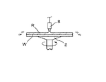
本発明の第2の実施の形態について説明する。この実施の形態は、図4記載の洗浄液供給ノズル5に気体供給手段を付加した実施の形態であるが、上述のノズルよりも吐出口50を長めに設定してある。具体的には、図7に示すように、現像液Dの液面よりも上方側であって洗浄液供給ノズル5の進行方向側の側壁面部に設けられた例えばエアーなどの気体をウェハWの表面に向かって噴出するための気体供給手段としての気体噴気口である吹き出し口70を備えている。この吹き出し口70は、例えば吐出口50の軸線(吐出方向)に対して角度θ例えば0°〜60°傾斜させるように設定されている。また当該吹き出し口70は、例えば直径0.4mmの複数の給気孔から構成され、例えば洗浄液供給ノズル5の長さ方向に間隔をおいて配置されている。更にまた、吹き出し口70は例えば洗浄液供給ノズル5の内部にて気体貯留部71を介して外部からの給気路72例えば配管の一端と接続され、また給気路72の他端は気体供給部73と接続されており、その途中には開閉バルブV3が設けられている。この場合、図5(a)、(b)に記載の工程を経て静止現像が行われたウェハWに対して、洗浄液供給ノズル5により上述と同様の条件で洗浄液Rが供給されると共に、吹き出し口70からウェハWに向かって例えば2.0リットル/分の流量でエアーを噴出する。なお、吹き出し口70は現像液Dの液面よりも下にあってもよいが、この場合には洗浄液供給ノズル5の吐出口50が汚れるので、頻繁に洗浄することが好ましい。従って、吹き出し口70は現像液Dの液面よりも上方に設定するのが得策である。
【0027】
上述の第2の実施の形態においては、供給ノズル5がスキャンされる際に、スキャン方向側にある吹き出し口70から前方側の現像液Dに向けて噴出された気体により、ウェハW上の現像液Dに液流れが起きてレジストの溶解生成物が巻き上げられ、その後に通過する吐出口50から吐出された洗浄液Rによる掃き出し作用と相俟って洗浄効果が向上する。このためウェハWの表面に溶解生成物が残るのが抑えられ、上述の場合と同様の効果を得ることができる。
【0028】
また吹き出し口70は、上述のように斜めに傾斜して設ける構成に限られず、図8(a)に示すように、洗浄液Rの吐出口50の直ぐ前の位置に吹き付けるように真下に向けてもよいし、また図8(b)に示すように、真下および斜めに設けるようにしてもよく、更にまた図8(c)に示すように、例えば図7に記載の斜めに傾斜した吹き出し口70から吹き出されたエアーが現像液Dの液面に到達する位置(図中の点P)に上方から吹き付けられるようにしてもよい。このような構成であっても、エアーを吹き付けることによりレジストの溶解生成物が巻き上げられて、上述の場合と同様の効果を得ることができる。
【0029】
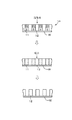
本発明においては、洗浄液供給ノズル5は、一のスリット形状の吐出口を備えた構成に限られず、例えば図10に洗浄液供給ノズル5についての一例を示すように、進行方向に沿って並ぶ複数例えば3個のスリット形状の吐出口50a、50b、50cを設ける構成であってもよく、更には各吐出口50a、50b、50cの夫々に流量調整が可能なように流量調整部例えば流量調整バルブV2a、V2b、V2cを設けるようにしてもよい。この場合、各吐出口の流量は同じに設定してもよいが、例えば粒子径の小さい不溶解物を先ず掃き出ししてから粒子径の大きいものを掃き出すようにするために例えば0.5〜4.0リットル/分の流量範囲において例えば前方側の吐出口50aの流量が最も少なく、吐出口50b、吐出口50cの順に流量が多くなるように設定するのが好ましい。このような構成であっても上述の場合と同様の効果を得ることができ、更には洗浄液Rの供給量を多くすることにより、短い洗浄時間で洗浄することができる。
【0030】
更に本発明においては、図5(c)に記載の洗浄を行った後に、続いて図9に示すように、スピン方式の洗浄を行うようにしてもよい。即ち、洗浄液供給ノズル5により上述と同様の条件で洗浄が行われて洗浄液供給ノズル5が後退した後、例えばウェハWの中心部に洗浄液Rを供給するための別の洗浄液供給ノズル8がウェハWの中心部に対向するように例えば2mm程度の高さ位置に設定され、次いで例えば100〜1000rpm程度の回転数にてウェハWを回転させると共に、例えば1リットル/分の流量で洗浄液RをウェハWの表面に供給する。所定の時間例えば5秒が経過すると、洗浄液Rの供給を停止してスピン乾燥が行われる。この場合、既述のスキャン方式の洗浄の作用と、遠心力を利用したスピン方式の洗浄の作用とが相俟ってより洗浄の効果が向上し、上述の場合と同様の効果を得ることができる。
【0031】
更にまた、本発明においては、ウェハWの表面に現像液Dを供給して静止現像が終了した後、洗浄液Rの供給を行う前に、スピンチャック2を回転させてウェハWを例えば100rpm〜1000rpm程度の回転数にて所定の時間例えば0.5〜3秒間回転さるようにしてもよい。この場合、洗浄液Rを供給する前にウェハW上の現像液Dを遠心力の作用によりある程度振り切っておくことができるので、続いて行われる洗浄液Rの洗浄の作用と併せて、より洗浄の効果が向上し、上述の場合と同様の効果を得ることができる。
【0032】
また本発明においては、吐出口50はスリット形状に限られず、例えばノズルの下面側に長手方向に沿って例えば直径0.4mm程度の吐出孔を間隔をおいて配列する構成であってもよい。更にまた、供給ノズル5と洗浄液供給ノズル6とを別個のノズルとする構成に限られず、例えば図11に示すように、供給路43、53を介して現像液供給部44と洗浄液供給部54とが夫々接続された共通の吐出口70を有する共通ノズル7を備えた構成とし、各バルブV1、バルブV2の切り換えにより現像液Dあるいは洗浄液Rを供給するようにしてもよい。
【0033】
続いて上述の現像装置を例えば現像ユニットに組み込んだ塗布・現像装置一例について図12及び図13を参照しながら説明する。図中B1は基板であるウエハWが例えば13枚密閉収納されたカセットCを搬入出するためのカセット載置部であり、カセットCを複数個載置可能な載置部91aを備えた載置台91と、この載置台91から見て前方の壁面に設けられる開閉部92と、開閉部92を介してカセットCからウエハWを取り出すための受け渡し手段93とが設けられている。
【0034】
カセット載置部B1の奥側には筐体100にて周囲を囲まれる処理部B2が接続されており、この処理部B2には手前側から順に加熱・冷却系のユニットを多段化した棚ユニットU1,U2,U3と、後述する塗布・現像ユニットを含む各処理ユニット間のウエハWの受け渡しを行う主搬送手段101A,101Bとが交互に配列して設けられている。即ち、棚ユニットU1,U2,U3及び主搬送手段101A,101Bはカセット載置部B1側から見て前後一列に配列されており、各々の接続部位には図示しないウエハ搬送用の開口部が形成されており、ウエハWは処理部B1内を一端側の棚ユニットU1から他端側の棚ユニットU2まで自由に移動できるようになっている。また主搬送手段101A,101Bは、カセット載置部B1から見て前後方向に配置される棚ユニットU1,U2,U3側の一面部と、後述する例えば右側の液処理ユニットU4,U5側の一面部と、左側の一面をなす背面部とで構成される区画壁102により囲まれる空間内に置かれている。また図中103,104は各ユニットで用いられる処理液の温度調節装置や温湿度調節用のダクト等を備えた温湿度調節ユニットである。
【0035】
液処理ユニットU4,U5は、例えば図13に示すように塗布液(レジスト液)や現像液といった薬液供給用のスペースをなす収納部105の上に、塗布ユニットCOT、図1、図2記載の現像装置を組み込んだ現像ユニットDEV及び反射防止膜形成ユニットBARC等を複数段例えば5段に積層した構成とされている。また既述の棚ユニットU1,U2,U3は、液処理ユニットU4,U5にて行われる処理の前処理及び後処理を行うための各種ユニットを複数段例えば10段に積層した構成とされている。
【0036】
処理部B2における棚ユニットU3の奥側には、例えば第1の搬送室106及び第2の搬送室107からなるインターフェイス部B3を介して露光部B4が接続されている。インターフェイス部B3の内部には処理部B2と露光部B4との間でウエハWの受け渡しを行うための2つの受け渡し手段108,109の他、棚ユニットU6及びバッファカセットC0が設けられている。
【0037】
この装置におけるウエハの流れについて一例を示すと、先ず外部からウエハWの収納されたカセットCが載置台91に載置されると、開閉部92と共にカセットCの蓋体が外されて受け渡し手段93によりウエハWが取り出される。そしてウエハWは棚ユニットU1の一段をなす受け渡しユニット(図示せず)を介して主搬送手段101Aへと受け渡され、棚ユニットU1〜U3内の一の棚にて、塗布処理の前処理として例えば疎水化処理、冷却処理が行われ、しかる後塗布ユニットCOTにてレジスト液が塗布される。こうして表面にレジスト膜が形成されると、ウエハWは棚ユニットU1〜U3の一の棚をなす加熱ユニットで加熱され、更に冷却された後棚ユニットU3の受け渡しユニットを経由してインターフェイス部B3へと搬入される。このインターフェイス部B3においてウエハWは例えば受け渡し手段108→棚ユニットU6→受け渡し手段109という経路で露光部B4へ搬送され、露光が行われる。露光後、ウエハWは逆の経路で主搬送手段101Aまで搬送され、現像ユニットDEVにて現像されることでレジストマスクが形成される。しかる後ウエハWは載置台91上の元のカセットCへと戻される。
【0038】
また本発明は、被処理基板に半導体ウエハ以外の基板、例えばLCD基板、フォトマスク用レチクル基板の処理にも適用できる。
【0039】
【実施例】
続いて本発明の効果を確認するために上述の現像装置を用いて行った実施例について説明する。
(実施例1)
本例は、本発明の第1の実施の形態に係る現像装置を用いた実施例1である。
この実施例1は、前段の工程にてレジストの塗布および露光処理がされた基板に対して、図5に記載の工程に基づいて現像処理を行ったものであり、その際洗浄液供給ノズル5の離間距離Lおよび洗浄時間Tを種々の設定値に設定した。そして現像処理後の基板の表面に対して表面欠陥検査(KLA-tencor製検査装置)を行って現像欠陥数を測定した。なお、検査においては、0.08μm以上の大きさの現像欠陥をカウントした。以下に具体的な試験条件を示す。
・基板:8インチサイズの半導体ウェハ
・現像液Dの液膜厚さ:1.5mm
・静止現像時間:60秒
・洗浄液供給ノズル5のスキャン速度:120mm/秒
・洗浄液Rの流量:2.0リットル/秒
・離間距離L:0.3mm、0.4mm、(0.6mm)、(1.0mm)、1.5mm、5mm、カッコ内のものは洗浄時間5秒にて実施。
・スキャン洗浄回数(洗浄時間):(各離間距離Lに対して)3回(5秒)、6回(10秒)
【0040】
(実施例1の結果と考察)
実施例1の結果を図14に示す。先ず5秒間の洗浄を行った場合についてみると、離間距離Lが1.5mmよりも大きく設定したときには欠陥数が65000(検出上限値)カウントされているが、1.5mm以下に設定すると欠陥数が低下し始め、0.6mm以下で急激に減少する。そして0.3mm、0.4mmで欠陥数が20程度になっている。また洗浄時間Tを10秒に設定した場合についてみると、離間距離Lが0.3mmおよび0.4mmで50程度、1.5mmでも50程度の欠陥数になっており、欠陥数にそれほど変化は見られないが、1.5mmよりも大きく設定すると欠陥数が増加している。即ち、洗浄液供給ノズル5の吐出口50の先端が現像液D中に浸っており、かつ離間距離Lを0.4mm以下に設定すれば欠陥数を少なくすることができることが確認された。
【0041】
(実施例2)
本例は、本発明の第2の実施の形態に係る現像装置を用いた実施例2である。この実施例2は、実施例1と同じく前段の工程にてレジストの塗布および露光処理がされた基板に対して、図5に記載の工程に基づいて現像処理を行ったものであるが、その際図7記載の洗浄液供給ノズル5を用いて洗浄液Rの供給を行った。現像欠陥の測定については、実施例1と同じである。以下に具体的な試験条件を示す。
・基板:8インチサイズの半導体ウェハ
・現像液Dの膜厚さ:1.5mm
・静止現像時間:60秒
・洗浄液供給ノズル5のスキャン速度:120mm/秒
・洗浄液Rの流量:2.0リットル/秒
・離間距離L:0.4mm、1.5mm
・エアーの流量:2.0リットル/秒
・傾斜角度θ:60°
・スキャン洗浄回数(洗浄時間):9回(15秒)
【0042】
(比較例1)
本例は、気体の供給を行わないことを除いて実施例2と同様の条件で行った比較例2である。
【0043】
(実施例2および比較例1の結果と考察)
実施例2および比較例1の結果を図15に併せて示す。気体の供給を行わない比較例1の結果が現像欠陥数40程度であるのに対し、気体の供給を行った実施例2においては現像欠陥数が10程度に抑えられている。即ち、気体を供給することにより現像液Dに液流れが起きてその液流れにより溶解生成物の掃き出しが行われ、洗浄液Rの掃き出しの作用と相俟って洗浄効果が向上することが確認された。
【0044】
【発明の効果】
以上のように本発明によれば、現像欠陥を低減することができ、また現像液の洗浄を短時間で行うことができる。
【図面の簡単な説明】
【図1】 本発明の現像装置の第1の実施の形態に係る現像装置を示す縦断面図である。
【図2】 本発明の現像装置の第1の実施の形態に係る現像装置を示す平面図である。
【図3】 前記現像装置に用いられる現像液供給ノズルを示す縦断面図である。
【図4】 前記現像装置に用いられる洗浄液供給ノズルを示す縦断面図である。
【図5】 前記現像装置を用いた現像処理の工程を示す説明図である。
【図6】 前記現像装置の洗浄工程の様子を示す説明図である。
【図7】 本発明の現像装置の第2の実施の形態に係る現像装置に用いられる洗浄液供給ノズルを示す縦断面図である。
【図8】 前記第2の実施の形態に係る現像装置に用いられる他の洗浄液ノズルを示す縦断面図である。
【図9】 本発明の現像装置に用いられる他の洗浄液ノズルを示す縦断面図である。
【図10】 本発明の現像装置の他の洗浄手法を示す説明図である。
【図11】 本発明の現像装置に用いられる他の洗浄液ノズルを示す縦断面図である。
【図12】 本発明に係る現像装置を組み込んだ塗布装置の一例を示す斜視図である。
【図13】 本発明に係る現像装置を組み込んだ塗布装置の一例を示す平面図である。
【図14】 本発明の効果を確認するために行った実施例を示す特性図である。
【図15】 本発明の効果を確認するために行った実施例を示す特性図である。
【図16】 現像処理工程の流れを示す説明図である。
【図17】 従来の現像装置を用いたときの現像処理の工程を示す説明図である。
【符号の説明】
W ウエハ
2 スピンチャック
30 外カップ
31 内カップ
4 現像液供給ノズル
40 吐出口
44 洗浄液供給部
5 洗浄液供給ノズル
50 吐出口
54 洗浄液供給部
6 制御部
70 給気口
73 気体供給部
V1、V2、V3 バルブ[0001]
BACKGROUND OF THE INVENTION
The present invention relates to a developing device for supplying a developing solution to a substrate that has been subjected to an exposure process by applying a resist to the surface of the substrate and performing the development process.And development processing methodAbout.
[0002]
[Prior art]
A mask for forming a circuit pattern on the surface of a semiconductor wafer or an LCD substrate of a liquid crystal display, for example, a photoresist solution (hereinafter referred to as a resist) is applied to the wafer surface, irradiated with light or the like, and then the resist For example, in the case of a negative type, a portion exposed to light is cured, and therefore, a non-cured portion, that is, a portion where the resist is easily dissolved is dissolved by a developer. For example, in the case of a positive resist, the exposed portion is dissolved with a developer.
[0003]
For example, a state in which a negative resist is developed will be described. As shown in FIG. 16, first, a developing solution is applied to the
[0004]
In the developing process using the conventional developing apparatus, as shown in FIG. 17A, the exposed wafer is held in a substantially horizontal posture, and the wafer W is rotated on the
[0005]
[Problems to be solved by the invention]
However, in recent years, the size of the wafer W has increased, and in the conventional method of washing away the developer D using the centrifugal force while rotating the wafer W, the centrifugal force that acts on the peripheral portion of the wafer W and the central portion The difference with the acting centrifugal force becomes large, and cleaning may be insufficient in the central portion where the centrifugal force is weak. That is, for example, the dissolved component of the resist in the valleys of the resist pattern has a high concentration, and further includes the one in which the dissolved resist component is precipitated, undissolved resist particles, and so on. It may be. When the centrifugal force is small, such a dissolved product has a stronger frictional force against the surface of the wafer W or the resist pattern wall than the centrifugal force. It may remain. And there exists a possibility that this melted product may dry and leave a development defect while adhering to the pattern surface (resist surface, base surface).
[0006]
On the other hand, a method for increasing the centrifugal force at the center by increasing the number of rotations of the wafer W has been studied. In this case, however, the centrifugal force at the peripheral portion is too strong and the resist pattern may be peeled off or fallen down. There is a concern that it will.
[0007]
The present invention has been made under such circumstances, and it is an object of the present invention to provide a technique capable of reducing development defects and cleaning a developing solution in a short time.
[0008]
[Means for Solving the Problems]
In the developing device of the present invention, a resist is applied to the surface of the substrate, and the substrate subjected to the exposure processing is developed.
A substrate holder for holding the substrate horizontally;
A developer supply nozzle for supplying a developer to the surface of the substrate held by the substrate holder;
A cleaning liquid supply nozzle for supplying a cleaning liquid to the surface of the substrate to which the developer is applied, having a discharge port formed over a length substantially equal to or longer than the width of the effective area of the substrate; ,
The cleaning liquid supply nozzle is moved from one end side to the other end side of the substrate at a height position where the lower end portion of the discharge port is below the liquid level of the developer and the distance from the surface of the substrate is 0.4 mm or less. And a moving mechanism that moves the head over.
[0009]
According to the developing device of the present invention, the lateral pushing action that occurs when the cleaning liquid discharged from the discharge port of the cleaning liquid supply nozzle collides with the surface of the substrate, and the pushing action by the side wall surface of the cleaning liquid supply nozzle. In combination, the developer containing the resist component on the substrate surface can be discharged. For this reason, since it can suppress that a developing solution and a resist component remain on the surface of a board | substrate, a pattern with few image development defects can be obtained.
[0010]
A developing device according to another invention is a developing device that develops a substrate subjected to exposure processing by applying a resist to the surface of the substrate.
A substrate holder for holding the substrate horizontally;
A developer supply nozzle for supplying a developer to the surface of the substrate held by the substrate holder;
A cleaning liquid supply nozzle for supplying a cleaning liquid to the surface of the substrate to which the developer is applied, having a discharge port formed over a length substantially equal to or longer than the width of the effective area of the substrate; ,
A gas blowing port provided on the side surface of the cleaning liquid supply nozzle on the traveling direction side and inclined forward;
A moving mechanism for moving the cleaning liquid supply nozzle from one end side to the other end side of the substrate at a height position where the lower end portion of the discharge port is below the level of the developer. To do.
[0011]
In addition, the cleaning liquid supply nozzle may have, for example, a plurality of discharge ports arranged in the advancing direction, and each of the discharge ports may be provided with a flow rate adjusting unit, for example. Further, for example, the cleaning liquid may be supplied after the substrate coated with the developer is rotated for a predetermined time. Furthermore, after the cleaning liquid is moved from one end side to the other end side of the substrate while discharging the cleaning liquid from the discharge port of the cleaning liquid supply nozzle, the substrate is removed while supplying the cleaning liquid to the central portion of the substrate, for example. You may make it perform the washing | cleaning to rotate. Furthermore,The gas blowing port is arranged in a predetermined direction with respect to the developer film formed on the substrate and disposed in the length direction of the cleaning liquid supply nozzle. Gas may be supplied at an angle.
[0012]
The development processing method of the present invention is a development processing method for developing a substrate that has been subjected to exposure processing by applying a resist to the surface of the substrate.
Supplying a developer to the surface of the substrate held horizontally to form a developer film;
A step of moving the cleaning liquid supply nozzle having a discharge port formed over a length substantially equal to or longer than the width of the effective area of the substrate a plurality of times from one end side to the other end side of the substrate;
A step of supplying a cleaning liquid toward the substrate during the movement of the cleaning liquid supply nozzle and cleaning the substrate,
The cleaning liquid supply nozzle is moved at a height position where a lower end portion of the discharge port is immersed in a developer or cleaning liquid on the substrate surface.
[0013]
In the step of supplying the cleaning liquid from the cleaning liquid supply nozzle toward the substrate, a gas may be ejected from the gas blowing port provided on the traveling direction side of the cleaning liquid supply nozzle toward the substrate. The gas blowing port is disposed along the length direction of the cleaning liquid supply nozzle and is inclined to the front side in the traveling direction, and is dissolved by blowing gas toward the substrate and melting out from the resist. The product may be swept out.
[0014]
A development processing method according to another invention is a development processing method for developing a substrate that has been subjected to exposure processing by applying a resist to the surface of the substrate.
Supplying a developer to the surface of the substrate held horizontally to form a developer film;
The cleaning liquid supply nozzle is placed at the height position where the lower end of the discharge port formed over a length substantially equal to or longer than the effective area of the substrate is immersed in the developer or cleaning liquid on the substrate surface. A step of moving a plurality of times from one end side to the other end side,
A step of supplying a cleaning liquid toward the substrate during the movement of the cleaning liquid supply nozzle and cleaning the substrate,
The plurality of movements includes a step of rotating the substrate around the vertical axis when the cleaning liquid supply nozzle is moved from one end side to the other end side of the substrate in the second and subsequent times. . Here, the cleaning liquid supply nozzle may have a plurality of discharge ports arranged in the traveling direction. Further, in the step of rotating the substrate around the vertical axis, the number of rotations of the substrate may be changed.
[0015]
DETAILED DESCRIPTION OF THE INVENTION
A first embodiment of a developing device according to the present invention will be described. FIG. 1 is a schematic sectional view of the developing device, and FIG. 2 is a schematic plan view. In the figure,
[0016]
Next, the developing
[0017]
Next, the cleaning
[0018]
The cleaning
[0019]
The
[0020]
Next, the process of developing using the above-described developing device will be described with reference to FIG. First, in a state where both the
[0021]
Subsequently, the
[0022]
Subsequently, the cleaning
[0023]
Here, how the surface of the wafer W is cleaned will be described in detail. As schematically shown in FIG. 6, when the cleaning
[0024]
Returning to FIG. 5, after the developer D on the surface of the wafer W is replaced with the cleaning liquid R as described above, the
[0025]
In the above-described embodiment, the lateral pushing action when the cleaning liquid R ejected from the
[0026]
A second embodiment of the present invention will be described. This embodiment is an embodiment in which a gas supply means is added to the cleaning
[0027]
In the above-described second embodiment, when the
[0028]
Further, the
[0029]
In the present invention, the cleaning
[0030]
Furthermore, in the present invention, after the cleaning shown in FIG.FIG.As shown in FIG. 4, spin-type cleaning may be performed. That is, after the cleaning
[0031]
Furthermore, in the present invention, after the developing solution D is supplied to the surface of the wafer W and the static development is completed, before the cleaning solution R is supplied, the
[0032]
In the present invention, the
[0033]
Next, an example of a coating / developing apparatus in which the above developing apparatus is incorporated in, for example, a developing unit will be described with reference to FIGS. In the figure, B1 is a cassette mounting portion for loading and unloading a cassette C in which, for example, 13 wafers W serving as substrates are hermetically stored, and a mounting table including a mounting
[0034]
A processing unit B2 surrounded by a
[0035]
The liquid processing units U4 and U5 are, for example, as shown in FIG. 13, a coating unit COT, as shown in FIG. 1 and FIG. 2, on a
[0036]
An exposure unit B4 is connected to an inner side of the shelf unit U3 in the processing unit B2 through an interface unit B3 including, for example, a
[0037]
An example of the flow of wafers in this apparatus is as follows. First, when the cassette C in which the wafers W are stored is mounted on the mounting table 91 from the outside, the lid of the cassette C is removed together with the opening / closing
[0038]
The present invention can also be applied to processing of a substrate other than a semiconductor wafer, such as an LCD substrate or a photomask reticle substrate, as a substrate to be processed.
[0039]
【Example】
Next, an example carried out using the above-described developing device to confirm the effect of the present invention will be described.
Example 1
This example is Example 1 using the developing device according to the first embodiment of the present invention.
In the first embodiment, the development process is performed on the substrate on which the resist is applied and exposed in the previous process based on the process shown in FIG. The separation distance L and cleaning time T were set to various set values. Then, surface defect inspection (inspection apparatus manufactured by KLA-tencor) was performed on the surface of the substrate after the development treatment to measure the number of development defects. In the inspection, development defects having a size of 0.08 μm or more were counted. Specific test conditions are shown below.
・ Substrate: 8 inch semiconductor wafer
・ Liquid film thickness of developer D: 1.5 mm
・ Still development time: 60 seconds
・ Scanning speed of cleaning liquid supply nozzle 5: 120 mm / second
・ Flow rate of cleaning liquid R: 2.0 liters / second
-Separation distance L: 0.3 mm, 0.4 mm, (0.6 mm), (1.0 mm), 1.5 mm, 5 mm, and the items in parentheses are washed for 5 seconds.
-Number of scan cleaning (cleaning time): 3 times (for each separation distance L) 3 times (5 seconds), 6 times (10 seconds)
[0040]
(Results and discussion of Example 1)
The result of Example 1 is shown in FIG. First, in the case of cleaning for 5 seconds, the number of defects is counted 65,000 (detection upper limit value) when the separation distance L is set to be larger than 1.5 mm, but the number of defects is set to 1.5 mm or less. Begins to decrease and decreases rapidly below 0.6 mm. The number of defects is about 20 at 0.3 mm and 0.4 mm. In the case where the cleaning time T is set to 10 seconds, the number of defects is about 50 when the separation distance L is 0.3 mm and 0.4 mm, and about 50 even when the distance is 1.5 mm. Although not seen, the number of defects increases when it is set larger than 1.5 mm. That is, it was confirmed that the number of defects can be reduced if the tip of the
[0041]
(Example 2)
This example is Example 2 using the developing device according to the second embodiment of the present invention. In this Example 2, as in Example 1, the resist was applied and exposed in the previous process, and the development process was performed based on the process shown in FIG. At this time, the cleaning liquid R was supplied using the cleaning
・ Substrate: 8 inch semiconductor wafer
-Film thickness of developer D: 1.5 mm
・ Still development time: 60 seconds
・ Scanning speed of cleaning liquid supply nozzle 5: 120 mm / second
・ Flow rate of cleaning liquid R: 2.0 liters / second
・ Separation distance L: 0.4 mm, 1.5 mm
・ Air flow rate: 2.0 liters / second
・ Inclination angle θ: 60 °
・ Number of scan cleaning (cleaning time): 9 times (15 seconds)
[0042]
(Comparative Example 1)
This example is Comparative Example 2 performed under the same conditions as in Example 2 except that gas supply is not performed.
[0043]
(Results and discussion of Example 2 and Comparative Example 1)
The results of Example 2 and Comparative Example 1 are also shown in FIG. The result of Comparative Example 1 in which no gas is supplied is about 40 development defects, whereas in Example 2 in which gas is supplied, the number of development defects is suppressed to about 10. That is, it is confirmed that by supplying the gas, a liquid flow is generated in the developer D, and the dissolved product is swept out by the liquid flow. It was.
[0044]
【The invention's effect】
As described above, according to the present invention, development defects can be reduced, and the developer can be washed in a short time.
[Brief description of the drawings]
FIG. 1 is a longitudinal sectional view showing a developing device according to a first embodiment of a developing device of the present invention.
FIG. 2 is a plan view showing the developing device according to the first embodiment of the developing device of the present invention.
FIG. 3 is a longitudinal sectional view showing a developer supply nozzle used in the developing device.
FIG. 4 is a longitudinal sectional view showing a cleaning liquid supply nozzle used in the developing device.
FIG. 5 is an explanatory view showing a development processing step using the developing device.
FIG. 6 is an explanatory diagram showing a state of a cleaning process of the developing device.
FIG. 7 is a longitudinal sectional view showing a cleaning liquid supply nozzle used in a developing device according to a second embodiment of the developing device of the present invention.
FIG. 8 is a longitudinal sectional view showing another cleaning liquid nozzle used in the developing device according to the second embodiment.
FIG. 9 is a longitudinal sectional view showing another cleaning liquid nozzle used in the developing device of the present invention.
FIG. 10 is an explanatory diagram showing another cleaning method of the developing device of the present invention.
FIG. 11 is a longitudinal sectional view showing another cleaning liquid nozzle used in the developing device of the present invention.
FIG. 12 is a perspective view showing an example of a coating apparatus incorporating the developing device according to the present invention.
FIG. 13 is a plan view showing an example of a coating apparatus incorporating a developing device according to the present invention.
FIG. 14 is a characteristic diagram showing an example carried out to confirm the effect of the present invention.
FIG. 15 is a characteristic diagram showing an example carried out to confirm the effect of the present invention.
FIG. 16 is an explanatory diagram showing a flow of a development processing step.
FIG. 17 is an explanatory diagram showing development processing steps when a conventional developing device is used.
[Explanation of symbols]
W wafer
2 Spin chuck
30 outside cup
31 inner cup
4 Developer supply nozzle
40 Discharge port
44 Cleaning liquid supply unit
5 Cleaning liquid supply nozzle
50 Discharge port
54 Cleaning liquid supply part
6 Control unit
70 Air supply port
73 Gas supply part
V1, V2, V3 valves
Claims (13)
基板を水平に保持する基板保持部と、
この基板保持部に保持された基板の表面に現像液を供給する現像液供給ノズルと、
前記基板の有効領域の幅とほぼ同じかそれ以上の長さに亘って形成された吐出口を有し、現像液が塗布された基板の表面に対して洗浄液を供給するための洗浄液供給ノズルと、
前記吐出口の下端部が現像液の液面よりも下でありかつ基板の表面との離間距離が0.4mm以下の高さ位置で前記洗浄液供給ノズルを、基板の一端側から他端側に亘って移動させる移動機構と、を備えたことを特徴とする現像装置。In a developing device for developing a substrate that has been subjected to exposure processing by applying a resist to the surface of the substrate,
A substrate holder for holding the substrate horizontally;
A developer supply nozzle for supplying a developer to the surface of the substrate held by the substrate holder;
A cleaning liquid supply nozzle for supplying a cleaning liquid to the surface of the substrate to which the developer is applied, having a discharge port formed over a length substantially equal to or longer than the width of the effective area of the substrate; ,
The cleaning liquid supply nozzle is moved from one end side to the other end side of the substrate at a height position where the lower end portion of the discharge port is below the liquid level of the developer and the distance from the surface of the substrate is 0.4 mm or less. And a moving mechanism for moving the developing device.
基板を水平に保持する基板保持部と、
この基板保持部に保持された基板の表面に現像液を供給する現像液供給ノズルと、
前記基板の有効領域の幅とほぼ同じかそれ以上の長さに亘って形成された吐出口を有し、現像液が塗布された基板の表面に対して洗浄液を供給するための洗浄液供給ノズルと、
前記洗浄液供給ノズルの進行方向側の側面部に設けられ、前方側に傾斜した気体噴気口と、
前記吐出口の下端部が現像液の液面よりも下になる高さ位置で前記洗浄液供給ノズルを基板の一端側から他端側に亘って移動させる移動機構と、を備えたことを特徴とする現像装置。In a developing device for developing a substrate that has been subjected to exposure processing by applying a resist to the surface of the substrate,
A substrate holder for holding the substrate horizontally;
A developer supply nozzle for supplying a developer to the surface of the substrate held by the substrate holder;
A cleaning liquid supply nozzle for supplying a cleaning liquid to the surface of the substrate to which the developer is applied, having a discharge port formed over a length substantially equal to or longer than the width of the effective area of the substrate; ,
A gas blowing port provided on the side surface of the cleaning liquid supply nozzle on the traveling direction side and inclined forward;
A moving mechanism for moving the cleaning liquid supply nozzle from one end side to the other end side of the substrate at a height position where the lower end portion of the discharge port is below the level of the developer. Developing device.
水平に保持された基板の表面に現像液を供給し現像液膜を形成する工程と、
この基板の有効領域の幅と略同じかそれ以上の長さに亘って形成された吐出口を有した洗浄液供給ノズルを当該基板の一端側から他端側に亘って複数回移動させる工程と、
この洗浄液供給ノズルの移動に際し前記基板に向けて洗浄液を供給して洗浄をする工程と、を含み、
前記洗浄液供給ノズルは、吐出口の下端部が前記基板表面上の現像液又は洗浄液に浸漬する高さ位置で移動させることを特徴とする現像処理方法。In a development processing method for developing a substrate that has been subjected to exposure processing by applying a resist to the surface of the substrate,
Supplying a developer to the surface of the substrate held horizontally to form a developer film;
A step of moving the cleaning liquid supply nozzle having a discharge port formed over a length substantially equal to or longer than the width of the effective area of the substrate a plurality of times from one end side to the other end side of the substrate;
A step of supplying a cleaning liquid toward the substrate during the movement of the cleaning liquid supply nozzle and cleaning the substrate,
The developing method according to claim 1, wherein the cleaning liquid supply nozzle is moved at a height position where a lower end portion of the discharge port is immersed in the developing solution or the cleaning solution on the substrate surface.
水平に保持された基板の表面に現像液を供給し現像液膜を形成する工程と、
この基板の有効領域の幅と略同じかそれ以上の長さに亘って形成された吐出口の下端部が当該基板表面上の現像液又は洗浄液に浸漬する高さ位置で、洗浄液供給ノズルを基板の一端側から他端側に亘って複数回移動させる工程と、
この洗浄液供給ノズルの移動に際し前記基板に向けて洗浄液を供給して洗浄をする工程と、を含み、
前記複数回の移動において、2回目以降に洗浄液供給ノズルを前記基板の一端側から他端側に亘って移動させるときに当該基板を鉛直軸回りに回転させる工程と、を含むことを特徴とする現像処理方法。In a development processing method for developing a substrate that has been subjected to exposure processing by applying a resist to the surface of the substrate,
Supplying a developer to the surface of the substrate held horizontally to form a developer film;
The cleaning liquid supply nozzle is placed at the height position where the lower end of the discharge port formed over a length substantially equal to or longer than the effective area of the substrate is immersed in the developer or cleaning liquid on the substrate surface. A step of moving a plurality of times from one end side to the other end side,
A step of supplying a cleaning liquid toward the substrate during the movement of the cleaning liquid supply nozzle and cleaning the substrate,
The plurality of movements includes a step of rotating the substrate around the vertical axis when the cleaning liquid supply nozzle is moved from one end side to the other end side of the substrate in the second and subsequent times. Development processing method.
Priority Applications (7)
| Application Number | Priority Date | Filing Date | Title |
|---|---|---|---|
| JP2002167565A JP4194302B2 (en) | 2002-06-07 | 2002-06-07 | Development device and development processing method |
| US10/515,635 US7387455B2 (en) | 2002-06-07 | 2003-05-16 | Substrate processing device, substrate processing method, and developing device |
| KR1020097018280A KR100959740B1 (en) | 2002-06-07 | 2003-05-16 | Substrate processing device |
| PCT/JP2003/006149 WO2003105201A1 (en) | 2002-06-07 | 2003-05-16 | Substrate processing device, substrate processing method, and developing device |
| AU2003234811A AU2003234811A1 (en) | 2002-06-07 | 2003-05-16 | Substrate processing device, substrate processing method, and developing device |
| KR1020047009165A KR100935286B1 (en) | 2002-06-07 | 2003-05-16 | Substrate processing device and developing device |
| TW092114445A TWI253098B (en) | 2002-06-07 | 2003-05-28 | Substrate processing apparatus, substrate processing method and developing apparatus |
Applications Claiming Priority (1)
| Application Number | Priority Date | Filing Date | Title |
|---|---|---|---|
| JP2002167565A JP4194302B2 (en) | 2002-06-07 | 2002-06-07 | Development device and development processing method |
Publications (3)
| Publication Number | Publication Date |
|---|---|
| JP2004014869A JP2004014869A (en) | 2004-01-15 |
| JP2004014869A5 JP2004014869A5 (en) | 2005-05-26 |
| JP4194302B2 true JP4194302B2 (en) | 2008-12-10 |
Family
ID=30434773
Family Applications (1)
| Application Number | Title | Priority Date | Filing Date |
|---|---|---|---|
| JP2002167565A Expired - Fee Related JP4194302B2 (en) | 2002-06-07 | 2002-06-07 | Development device and development processing method |
Country Status (1)
| Country | Link |
|---|---|
| JP (1) | JP4194302B2 (en) |
Families Citing this family (4)
| Publication number | Priority date | Publication date | Assignee | Title |
|---|---|---|---|---|
| JP4410076B2 (en) | 2004-10-07 | 2010-02-03 | 東京エレクトロン株式会社 | Development processing equipment |
| JP4641964B2 (en) | 2006-03-30 | 2011-03-02 | 大日本スクリーン製造株式会社 | Substrate processing apparatus and substrate processing method |
| JP4937772B2 (en) * | 2007-01-22 | 2012-05-23 | 東京エレクトロン株式会社 | Substrate processing method |
| KR20130125751A (en) * | 2010-07-09 | 2013-11-19 | 스미또모 베이크라이트 가부시키가이샤 | Method for forming cured film |
-
2002
- 2002-06-07 JP JP2002167565A patent/JP4194302B2/en not_active Expired - Fee Related
Also Published As
| Publication number | Publication date |
|---|---|
| JP2004014869A (en) | 2004-01-15 |
Similar Documents
| Publication | Publication Date | Title |
|---|---|---|
| US7976896B2 (en) | Method of processing a substrate and apparatus processing the same | |
| JP4324527B2 (en) | Substrate cleaning method and developing apparatus | |
| KR101493647B1 (en) | Substrate cleaning method and substrate cleaning apparatus | |
| JP3265238B2 (en) | Liquid film forming apparatus and method | |
| JP4734063B2 (en) | Substrate cleaning apparatus and substrate cleaning method. | |
| JP4451450B2 (en) | Substrate processing method and substrate processing apparatus | |
| TWI619190B (en) | Liquid processing method, memory medium and liquid processing device | |
| TWI253098B (en) | Substrate processing apparatus, substrate processing method and developing apparatus | |
| WO2005098919A1 (en) | Board cleaning apparatus, board cleaning method, and medium with recorded program to be used for the method | |
| JP3899319B2 (en) | Liquid processing apparatus and liquid processing method | |
| TW201840370A (en) | Coating film removal device, coating film removal method, and storage medium | |
| TWI797159B (en) | Substrate processing method, substrate processing device, and storage medium | |
| JP2000147787A (en) | Method and device for developing | |
| JP4194302B2 (en) | Development device and development processing method | |
| JP7001400B2 (en) | Board processing equipment | |
| JP3573445B2 (en) | Developing device and cleaning device | |
| JP4343031B2 (en) | Substrate processing method and substrate processing apparatus | |
| JP3869326B2 (en) | Development processing method | |
| JP2004014869A5 (en) | ||
| JP7329418B2 (en) | Substrate processing method and substrate processing apparatus | |
| JP3990322B2 (en) | Substrate drying method and apparatus | |
| JP3266229B2 (en) | Processing method | |
| JP3453022B2 (en) | Developing device | |
| JP7191216B2 (en) | Substrate processing method | |
| TWI834229B (en) | Substrate processing method and substrate processing device |
Legal Events
| Date | Code | Title | Description |
|---|---|---|---|
| A521 | Written amendment |
Free format text: JAPANESE INTERMEDIATE CODE: A523 Effective date: 20040726 |
|
| A621 | Written request for application examination |
Free format text: JAPANESE INTERMEDIATE CODE: A621 Effective date: 20040726 |
|
| A131 | Notification of reasons for refusal |
Free format text: JAPANESE INTERMEDIATE CODE: A131 Effective date: 20071023 |
|
| A521 | Written amendment |
Free format text: JAPANESE INTERMEDIATE CODE: A523 Effective date: 20071113 |
|
| TRDD | Decision of grant or rejection written | ||
| A01 | Written decision to grant a patent or to grant a registration (utility model) |
Free format text: JAPANESE INTERMEDIATE CODE: A01 Effective date: 20080902 |
|
| A01 | Written decision to grant a patent or to grant a registration (utility model) |
Free format text: JAPANESE INTERMEDIATE CODE: A01 |
|
| A61 | First payment of annual fees (during grant procedure) |
Free format text: JAPANESE INTERMEDIATE CODE: A61 Effective date: 20080922 |
|
| R150 | Certificate of patent or registration of utility model |
Free format text: JAPANESE INTERMEDIATE CODE: R150 Ref document number: 4194302 Country of ref document: JP Free format text: JAPANESE INTERMEDIATE CODE: R150 |
|
| FPAY | Renewal fee payment (event date is renewal date of database) |
Free format text: PAYMENT UNTIL: 20111003 Year of fee payment: 3 |
|
| FPAY | Renewal fee payment (event date is renewal date of database) |
Free format text: PAYMENT UNTIL: 20111003 Year of fee payment: 3 |
|
| FPAY | Renewal fee payment (event date is renewal date of database) |
Free format text: PAYMENT UNTIL: 20141003 Year of fee payment: 6 |
|
| R250 | Receipt of annual fees |
Free format text: JAPANESE INTERMEDIATE CODE: R250 |
|
| R250 | Receipt of annual fees |
Free format text: JAPANESE INTERMEDIATE CODE: R250 |
|
| R250 | Receipt of annual fees |
Free format text: JAPANESE INTERMEDIATE CODE: R250 |
|
| LAPS | Cancellation because of no payment of annual fees |