JP4166397B2 - Manufacturing method of optical member - Google Patents
Manufacturing method of optical member Download PDFInfo
- Publication number
- JP4166397B2 JP4166397B2 JP2000010028A JP2000010028A JP4166397B2 JP 4166397 B2 JP4166397 B2 JP 4166397B2 JP 2000010028 A JP2000010028 A JP 2000010028A JP 2000010028 A JP2000010028 A JP 2000010028A JP 4166397 B2 JP4166397 B2 JP 4166397B2
- Authority
- JP
- Japan
- Prior art keywords
- lens
- optical member
- resin
- light shielding
- gate
- Prior art date
- Legal status (The legal status is an assumption and is not a legal conclusion. Google has not performed a legal analysis and makes no representation as to the accuracy of the status listed.)
- Expired - Fee Related
Links
- 230000003287 optical effect Effects 0.000 title claims description 83
- 238000004519 manufacturing process Methods 0.000 title claims description 25
- 239000011347 resin Substances 0.000 claims description 41
- 229920005989 resin Polymers 0.000 claims description 41
- 230000005540 biological transmission Effects 0.000 claims description 18
- 238000000465 moulding Methods 0.000 claims description 17
- 230000000694 effects Effects 0.000 claims description 10
- 238000000034 method Methods 0.000 claims description 4
- 238000005520 cutting process Methods 0.000 description 10
- 238000010586 diagram Methods 0.000 description 6
- 201000009310 astigmatism Diseases 0.000 description 5
- 230000000903 blocking effect Effects 0.000 description 5
- 238000004904 shortening Methods 0.000 description 4
- 230000002411 adverse Effects 0.000 description 2
- 238000002347 injection Methods 0.000 description 2
- 239000007924 injection Substances 0.000 description 2
- 230000002093 peripheral effect Effects 0.000 description 2
- 238000009826 distribution Methods 0.000 description 1
- 238000005516 engineering process Methods 0.000 description 1
- 230000001678 irradiating effect Effects 0.000 description 1
- 239000000463 material Substances 0.000 description 1
- 230000013011 mating Effects 0.000 description 1
- 230000000149 penetrating effect Effects 0.000 description 1
- 238000005498 polishing Methods 0.000 description 1
- 210000001747 pupil Anatomy 0.000 description 1
- 238000003892 spreading Methods 0.000 description 1
Images


Classifications
-
- G—PHYSICS
- G02—OPTICS
- G02B—OPTICAL ELEMENTS, SYSTEMS OR APPARATUS
- G02B27/00—Optical systems or apparatus not provided for by any of the groups G02B1/00 - G02B26/00, G02B30/00
- G02B27/58—Optics for apodization or superresolution; Optical synthetic aperture systems
-
- G—PHYSICS
- G11—INFORMATION STORAGE
- G11B—INFORMATION STORAGE BASED ON RELATIVE MOVEMENT BETWEEN RECORD CARRIER AND TRANSDUCER
- G11B7/00—Recording or reproducing by optical means, e.g. recording using a thermal beam of optical radiation by modifying optical properties or the physical structure, reproducing using an optical beam at lower power by sensing optical properties; Record carriers therefor
- G11B7/12—Heads, e.g. forming of the optical beam spot or modulation of the optical beam
- G11B7/135—Means for guiding the beam from the source to the record carrier or from the record carrier to the detector
- G11B7/1372—Lenses
- G11B7/1374—Objective lenses
-
- G—PHYSICS
- G11—INFORMATION STORAGE
- G11B—INFORMATION STORAGE BASED ON RELATIVE MOVEMENT BETWEEN RECORD CARRIER AND TRANSDUCER
- G11B7/00—Recording or reproducing by optical means, e.g. recording using a thermal beam of optical radiation by modifying optical properties or the physical structure, reproducing using an optical beam at lower power by sensing optical properties; Record carriers therefor
- G11B7/12—Heads, e.g. forming of the optical beam spot or modulation of the optical beam
- G11B7/22—Apparatus or processes for the manufacture of optical heads, e.g. assembly
Landscapes
- Physics & Mathematics (AREA)
- Optics & Photonics (AREA)
- General Physics & Mathematics (AREA)
- Optical Head (AREA)
- Moulds For Moulding Plastics Or The Like (AREA)
Description
【0001】
【発明の属する技術分野】
本発明は、光学装置に用いられる樹脂製のレンズ等に適用して好適な光学部材の製造方法に関する。
【0002】
【従来の技術】
近年、例えば光ピックアップ装置などの光学装置では安価に製造できる樹脂製のレンズの需要が高まっている。通常、このようなレンズは成形型を用いた樹脂成形によって製造されている。
【0003】
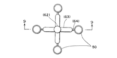
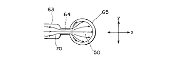
図8は従来の成形により製造されたゲートが切り離される前のレンズ50を示す平面図、図9は図8における9−9断面図、図10は樹脂70のキャビティ65内への充填状態を説明するための説明図である。
【0004】
従来のレンズ50は、図9に示すように、成形型60と61を用いて樹脂成形されていた。これら成形型60、61は、樹脂の注入口であるスプルー62と、流れの路にあたるランナー63と、成形品(レンズ50)が成形されるキャビティ65と、ランナー63からキャビティ65への流入口にあたるゲート64を備えている。
【0005】
そして、レンズ50が成形されるキャビティ65においては、レンズ50の側壁面(外周面)の一部に相当する位置にゲート64を設けて、このゲート64を流入口としてキャビティ65内に樹脂70を充填するようにしていた。すなわち、図10に示すように、樹脂70がキャビティ65内へ充填されるときには、樹脂70はゲート64からこのゲート64と対向するキャビティ65の側壁面側へほぼ一方向に流入するようになっている。そして、キャビティ65内が樹脂70で完全に満たされた後に、樹脂70は冷却されてレンズ50が完成する。
【0006】
【発明が解決しようとする課題】
しかしながら、このように製造されたレンズ50は、樹脂70のほぼ一方向(x方向)の流れに沿った歪みを生じ、その結果、例えば、樹脂70の流れの方向であるx方向とx方向と直交する方向で光の焦点位置が一致しないというように、いわゆる非点収差が発生して、レンズ50が方向性を持つ問題点があった。そのため、このレンズ50を光学装置に搭載するときには、レンズ50の光軸回りの位置を例えば光学装置の光学系として非点収差が最小となるように特定してから固定しなければならず、作業性が悪くなる問題があった。
【0007】
本発明の目的は、光軸回りで方向性を持たない光学部材の製造方法を提供することにある。
【0008】
【課題を解決するための手段】
上記課題を解決するための第1の解決手段として、光軸を有する光学部材を成形型を用いた樹脂成形によって製造するための製造方法であって、前記光学部材の光の透過面あるいは反射面における前記光軸位置に対応して前記成形型にゲートを設け、前記成形型の前記ゲート位置部分に前記透過面あるいは前記反射面よりも粗い粗面を形成し、前記ゲートから樹脂を注入するとともに、前記ゲート位置部分の前記光学部材に前記粗面を転写し、前記光学部材の前記ゲート位置部分に対応した所定の箇所に光の透過あるいは反射を遮る遮光帯である遮光面を形成することを特徴とするものである。
【0010】
さらに、第2の解決手段として、前記遮光面は前記透過面あるいは前記反射面よりも突出させて形成するようにしたことを特徴とするものである。
【0011】
さらに、第3の解決手段として、前記光学部材はレンズであり、前記遮光帯を該レンズの超解像効果のための遮光マスクに利用するようにしたことを特徴とするものである。
【0014】
【発明の実施の形態】
本発明の実施の形態である光学部材の製造方法及びその製造方法で製造した光学部材について、図面を用いて以下に説明する。
【0015】
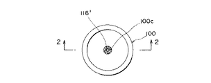
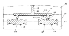
図1は、本発明の製造方法で製造したレンズ100を示す平面図、図2は図1における2−2断面図、図3は成形型110〜112とこの成形型に充填された樹脂120を示す一部断面図、図4はレンズ100を成形型110〜112から取り出す状態を示す説明図、図5は樹脂120のキャビティ117内への充填状態を説明するための説明図である。
【0016】
樹脂成形により形成される光学部材すなわちレンズ100は、図1、図2に示すように、透過面である2つのレンズ面100aと100bからなる凸レンズである。そして、レンズ100の成形時において、レンズ面100aにおける光軸N位置にこの光軸Nを略中心とした円形断面のゲートすなわちピンポイントゲート116(図3参照)を配設するようになっている。図中116′はピンポイントゲート116における樹脂120の切断部を示している。
【0017】
また、レンズ面100aには、切断部116′を取り囲み、かつ、ほぼ同軸状に形成したドーナツ状の凹部100dが形成されており、凹部100dの内底面の全面には遮光帯すなわち遮光面100cが形成されている。遮光面100cはレンズ面100a、100bよりも成形面を粗く形成することによって構成している。このようにして、遮光面100cは光の透過を遮るようになっている。
【0018】
次に、レンズ100の製造方法の実施の形態について説明する。
【0019】
図3、図4に示すように、レンズ100は成形型110と111と112を主に用いて樹脂成形される。これら成形型110、111、112は、樹脂の注入口であるスプルー113と、流れの路にあたるランナー114、115と、成形品(レンズ100)が成形されるキャビティ117と、ランナー114からキャビティ117への流入口にあたるピンポイントゲート116を備えている。
【0020】
そして、成形型110と111との合わせ面に横長のランナー114を形成し、このランナー114の中央部に連結するように成形型110の上方からスプルー113が貫通して形成されている。また、成形型111にはランナー114の両端部側から下方に向かって配設した2つのランナー115と、このランナー115の下端部からキャビティ117に貫通する2つのピンポイントゲート116が形成されている。
【0021】
また、それぞれのピンポイントゲート116に対応して成形型111の下面に形成されたキャビティ117には、レンズ100のレンズ面100aと凹部100dと遮光面100cを形成するためのそれぞれ、曲面117cと、曲面117cの中心(光軸N)位置で曲面117cよりも下方に突出して形成した円筒状の突出部117bと、突出部117bの先端面に形成した粗面117aとを設けてある。また、突出部117bの中心を貫通するように上述したピンポイントゲート116が設けられている。
【0022】
一方、成形型112の上面には、レンズ100のレンズ面100bを形成するための曲面117dが形成されている。なお、曲面117cと117dは研磨加工等により精密な表面に仕上げられている。また、粗面117aは曲面117c、117dに比べて充分に粗い表面となるように加工されているものである。
【0023】
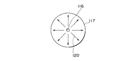
このように構成された成形型110〜112により、レンズ100が成形される。すなわち、スプルー113より所定の圧力により樹脂120が注入される。そして、図5に示すように、樹脂120がキャビティ117内へ充填されるときには、樹脂120はぽピンポイントゲート116からキャビティ117の側壁面(内周面)へ放射状に流入されるようになっている。そして、キャビティ117内が樹脂120で完全に満たされた後に、樹脂120は冷却されてレンズ100が完成する。
【0024】
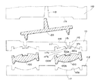
また、図4に示すように、レンズ100を成形型110〜112から取り出すときには、成形型110〜112に設けた図示しない切断手段によりピンポイントゲート116部分の樹脂120が切断されるようになっている。このレンズ100側の切断部116′(図2参照)の切断面は遮光面100cと同様に光を遮断できるような粗面となるように切断することが好ましい。なお、成形型110〜112に切断手段を設けないで、レンズ100を成形型111から取り出すときの引張力によってピンポイントゲート116部分の樹脂120を切断するようにしてもよい。このときは、引張力がレンズ100の特性に悪影響を及ぼさない程度にピンポイントゲート116の断面積をできるかぎり小さくしておくことが好ましい。
【0025】
このように製造されたレンズ100は、図5を用いて説明したように、樹脂120はキャビティ117内で放射状に沿って充填され、すなわち光軸Nに対して回転対称に充填されるので、従来のレンズ50のように非点収差が発生することがなく、レンズ100が方向性を持つことがない。したがって、このレンズ100を光学装置に搭載するときには、レンズ100の光軸N回りの位置を気にせずに固定してよいので、作業性が良くなる効果が得られる。
【0026】
また、図2に示すように、遮光面100cと切断部116′を凹部100dの内底面に設けているので、これらがレンズ面100aよりも突出することがなく、他の部材を接近させて配置することが可能となる。
【0027】
なお、本実施の形態では、成形型110〜112によって、レンズ100を2個成形する2個取りとしたが、これに限らず、1個取りあるいは3個以上の多数個取りとしてもよい。
【0028】
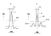
次に、レンズ100に設けた遮光面100cの作用について図6A、Bを用いて説明する。
【0029】
図6Aはレンズ100に遮光面100cを設けない場合の光の集光状態を説明するための説明図、図6Bはレンズ100に遮光面100cを設けた場合の光の集光状態を説明するための説明図である。
【0030】
レンズ100を例えば、光ピックアップ装置に用いる対物レンズに適用した場合には、レンズ100によって集光された光すなわちレーザ光を光ディスクの情報記録面に照射して情報の記録あるいは再生が行われる。このとき、集光されたレーザ光(集光スポット)の径が小さいほど光ディスクにおける情報の記録密度を向上させることができる。
【0031】
集光スポットを小さくする方法として、レーザ光の波長を短くすることと、超解像効果を用いることが知られている。このうち、超解像効果はレンズの中心部(瞳位置)に円形状あるいは方形状などの遮光マスクを設置することによって得られ、波動光学的な回折限界で決定される集光スポット径よりも小さくすることができる。一方、短波長化は、短波長のレーザ光を出射するレーザダイオードを使用することによって実現できるが、レーザダイオードを短波長化するためには常に最先端の技術導入が必要でありコストがアップする問題点がある。
【0032】
図6A、Bは同じ波長のレーザ光を用いたときに、レンズ100に遮光面100c(遮光マスク)を設けない(切断部116′も含まず)場合(A)と設けた場合(B)の光ディスクに集光された状態における集光スポットの強度分布を定性的に示している。図6Aに示すメインビーム200のビーム径D1(半値幅)に対して、図6Bにおけるメインビーム201のビーム径D2(半値幅)が細くなっている。このときメインビーム201の両側にはサイドローブと呼ばれる2次的なレーザ光201a、201aが発生するが、光ディスクの記録/再生にはメインビーム201のみを用いることができるので、レーザ光201a、201aが記録/再生動作に悪影響を及ぼすことはない。
【0033】
このように、レンズ100を光ピックアップ装置に搭載した場合には、波長を短波長化することなく安価なレーザダイオードを用いて集光スポット径を小さくすることができ、高密度な光ディスクの記録あるいは再生に対応することができるメリットが得られる。なお、光ピックアップ装置に限らず他の光学装置にも適用することができる。
【0034】
次に、本発明の他の実施の形態について、図7を用いて説明する。
【0035】
図7は本発明の他の実施の形態のレンズ300を示す断面図である。なお、第1の実施の形態のレンズ100と共通部分には共通の符号を付してある。
【0036】
レンズ300では、レンズ面100aの光軸N位置にピンポイントゲート116を配置するのは第1の実施の形態と同様であるが、本実施の形態では、遮光面300cをレンズ面100aよりも突出した位置に配設している。すなわち、レンズ面100aの光軸Nと同軸で、かつ、レンズ面100aよりも突出した円柱状の突出部300dを形成し、この突出部300dの上端面に遮光面300cを形成している。なお、遮光面300cの中央部にピンポイントゲート116部分の切断部116′が配置される。
【0037】
このようにしたことで、第1の実施の形態と同様の効果が得られるだけでなく、レンズ300を成形型から取り出した後に、切断部116′を再度切断して遮光面300c位置に揃えるような場合に、切断位置をレンズ面100aから上方に離れた位置にすることができるので、レンズ面100aを傷つけることなく切断作業ができる。
【0038】
なお、レンズ300の成形時に、突出部300dの上端面を粗面ではなく平坦な加工面としておき、レンズ300を成形型から取り出した後に、切断部116′を含めた突出部300dの上端面を粗く研いて遮光面300cを形成するようにしてもよい。
【0039】
以上説明した2つの実施の形態においては、ピンポイントゲート116の断面を円形としたが、これに限らず、方形状としても良い。また、遮光面100c、300cの外形を円形としたが、これに限らず、方形状としても良い。
【0040】
また、光学部材として、レンズ100、300を実施の形態として説明したが、これに限らず、対物レンズの他、コリメートレンズ、シリンドリカルレンズ等でもよいし、反射ミラー、ハーフミラー、及びビームスプリッタ等でもよい。
【0041】
以上説明したように、本発明の製造方法で製造した光学部材によれば、光軸を有する光学部材であって、該光学部材は樹脂成形により形成され、光の透過面あるいは反射面における前記光軸位置を樹脂の流入口であるゲート位置とし、該ゲート位置部分に光の透過あるいは反射を遮る遮光帯を設けたことにより、光学部材は、樹脂が光軸部分のゲートから放射状に広がって充填されて形成されているので、すなわち光軸に対して回転対称に充填されているので、従来の一方向の樹脂の充填によって形成されたレンズのように非点収差が発生することがなく、光学部材が方向性を持つことをなくすことができる。また、この光学部材を光学装置に搭載するときには、光学部材の光軸回りの位置を気にせずに固定してよいので、作業性が良くすることができる。また、光学部材を例えばレンズとした場合には、遮光帯を利用して波長を短波長化することなく集光スポット径を小さくする作用を得ることができる。
【0042】
さらに、遮光帯は透過面あるいは反射面よりも粗い面で形成された遮光面であることにより、遮光帯は透過面あるいは反射面に比べて粗く形成するだけでよいので光学部材を簡単に構成できコストも安価なものとすることができる。
【0043】
さらに、遮光面は透過面あるいは反射面よりも突出させて形成したことにより、例えば、光学部材を成形型から取り出した後に、ゲート位置の樹脂を切断して所定の位置に揃えるような場合に、切断位置を透過面あるいは反射面から離れた位置にすることができるので、透過面あるいは反射面を傷つけることなく切断作業ができる。
【0044】
さらに、記光学部材はレンズであり、遮光帯を該レンズの超解像効果のための遮光マスクに利用したことにより、例えば、レンズを光ピックアップ装置に適用した場合には、波長を短波長化することなく、例えば安価なレーザダイオードから出射するレーザ光を用いて集光スポット径を小さくすることができ、高密度な光ディスクの記録あるいは再生に対応することができるメリットが得られる。
【0045】
【発明の効果】
以上説明したように、本発明の光学部材の製造方法によれば、光軸を有する光学部材を成形型を用いた樹脂成形によって製造するための製造方法であって、前記光学部材の光の透過面あるいは反射面における前記光軸位置に対応して前記成形型にゲートを設け、該ゲートから樹脂を注入するとともに、前記光学部材の前記ゲート位置部分に対応した所定の箇所に遮光帯を配設することにより、光学部材は、樹脂が光軸部分のゲートから放射状に広がって充填されて形成されるので、すなわち光軸に対して回転対称に充填されるので、従来の一方向の樹脂の充填によって形成されたレンズのように非点収差が発生することがなく、方向性を持つことのない光学部材を簡単に製造できる。また、光学部材を例えばレンズとした場合には、遮光帯を利用して波長を短波長化することなく集光スポット径を小さくする作用を得ることのできるレンズを簡単に製造することができる。
【0046】
さらに、成形型のゲート位置部分に透過面あるいは反射面よりも粗い粗面を形成し、前記ゲート位置部分の光学部材に前記粗面を転写し遮光帯である遮光面を形成することにより、光学部材の遮光帯に対応した位置の成形型に透過面あるいは反射面に比べて粗い粗面を形成するだけでよいので光学部材を簡単に製造できコストも安価なものとすることができる。
【図面の簡単な説明】
【図1】 本発明の製造方法で製造したレンズ100を示す平面図である。
【図2】 本発明の製造方法で製造したレンズ100に係り、図1における2−2断面図である。
【図3】 本発明の製造方法で製造したレンズ100に係り、成形型110〜112とこの成形型に注入された樹脂120を示す一部断面図である。
【図4】 本発明の製造方法で製造したレンズ100に係り、レンズ100を成形型110〜112から取り出す状態を示す説明図である。
【図5】 本発明の製造方法で製造したレンズ100に係り、樹脂120のキャビティ117内への充填状態を説明するための説明図である。
【図6】 本発明の製造方法で製造したレンズ100に係り、Aはレンズ100に遮光面100cを設けない場合の光の集光状態を説明するための説明図、Bはレンズ100に遮光面100cを設けた場合の光の集光状態を説明するための説明図である。
【図7】 本発明の製造方法で製造した他の形態のレンズ300を示す断面図である。
【図8】 従来のレンズ50に係り、従来の成形により製造されたゲートが切り離される前のレンズ50を示す平面図である。
【図9】 従来のレンズ50に係り、図8における9−9断面図である。
【図10】 従来のレンズ50に係り、樹脂70のキャビティ65内への充填状態を説明するための説明図である。
【符号の説明】
100、300 レンズ
100a、100b レンズ面
100c、300c 遮光面
100d 凹部
110、111、112 成形型
113 スプルー
114、115 ランナー
116 ピンポイントゲート
117 キャビティ
120 樹脂
300d 突出部[0001]
BACKGROUND OF THE INVENTION
The present invention relates to a manufacturing method of application to suitable optical member made of resin such as lenses used in optical devices.
[0002]
[Prior art]
In recent years, for example, an optical device such as an optical pickup device has been increasingly demanded for a resin lens that can be manufactured at low cost. Usually, such a lens is manufactured by resin molding using a mold.
[0003]
FIG. 8 is a plan view showing the
[0004]
The
[0005]
In the
[0006]
[Problems to be solved by the invention]
However, the
[0007]
An object of the present invention is to provide a method for manufacturing an optical Faculty member around the optical axis has a given directionality such.
[0008]
[Means for Solving the Problems]
As a first means for solving the above-mentioned problem , there is provided a manufacturing method for manufacturing an optical member having an optical axis by resin molding using a molding die, wherein the light transmitting surface or reflecting surface of the optical member is used. A gate is provided in the mold corresponding to the optical axis position in the mold, a rough surface rougher than the transmission surface or the reflection surface is formed in the gate position portion of the mold, and resin is injected from the gate. Transferring the rough surface to the optical member at the gate position portion, and forming a light blocking surface as a light blocking zone for blocking light transmission or reflection at a predetermined position corresponding to the gate position portion of the optical member. It is a feature.
[0010]
Further, as a second solving means, the light shielding surface is formed so as to protrude from the transmission surface or the reflection surface.
[0011]
Further, as a third solving means, the optical member is a lens, and the light shielding band is used as a light shielding mask for a super-resolution effect of the lens.
[0014]
DETAILED DESCRIPTION OF THE INVENTION
An optical member manufactured by the manufacturing method and the manufacturing method of the embodiment der Ru optical engine material of the present invention will be described below with reference to the drawings.
[0015]
FIG. 1 is a plan view showing a
[0016]
As shown in FIGS. 1 and 2, the optical member formed by resin molding, that is, the
[0017]
Further, the
[0018]
Next, an embodiment of a method for manufacturing the
[0019]
As shown in FIGS. 3 and 4, the
[0020]
A horizontally
[0021]
Further, in the
[0022]
On the other hand, a curved surface 117 d for forming the
[0023]
The
[0024]
As shown in FIG. 4, when the
[0025]
In the
[0026]
Further, as shown in FIG. 2, since the
[0027]
In the present embodiment, two
[0028]
Next, the effect | action of the light-shielding
[0029]
6A is an explanatory diagram for explaining a light condensing state when the
[0030]
When the
[0031]
As a method for reducing the focused spot, it is known to shorten the wavelength of the laser beam and to use the super-resolution effect. Of these, the super-resolution effect is obtained by installing a circular or rectangular light-shielding mask at the center of the lens (pupil position), which is larger than the focused spot diameter determined by the wave optical diffraction limit. Can be small. On the other hand, shortening the wavelength can be realized by using a laser diode that emits a laser beam with a short wavelength. However, in order to shorten the wavelength of the laser diode, it is always necessary to introduce the most advanced technology, which increases the cost. There is a problem.
[0032]
6A and 6B, when laser light having the same wavelength is used, the
[0033]
Thus, when the
[0034]
Next, another embodiment of the present invention will be described with reference to FIG.
[0035]
FIG. 7 is a cross-sectional view showing a
[0036]
In the
[0037]
By doing so, not only the same effects as in the first embodiment can be obtained, but also after the
[0038]
When the
[0039]
In the two embodiments described above, the
[0040]
Further, although the
[0041]
As described on the following, according to the optical member produced by the production method of the present invention, an optical member having an optical axis, the optical member is formed by resin molding, the in transmitting surface or a reflection surface of the light By setting the optical axis position as the gate position, which is the resin inlet, and providing a light-shielding band that blocks light transmission or reflection at the gate position part, the optical member spreads radially from the gate of the optical axis part. Since it is filled and formed, that is, it is filled in a rotationally symmetrical manner with respect to the optical axis, astigmatism does not occur as in the conventional lens formed by filling the resin in one direction, The optical member can be prevented from having directionality. Further, when this optical member is mounted on an optical device, the workability can be improved because the optical member may be fixed without worrying about the position of the optical member around the optical axis. Further, when the optical member is, for example, a lens, it is possible to obtain an effect of reducing the diameter of the focused spot without shortening the wavelength by using a light shielding band.
[0042]
Further, since the light shielding band is a light shielding surface formed with a rougher surface than the transmission surface or the reflection surface, the light shielding band only needs to be formed rougher than the transmission surface or the reflection surface, so that the optical member can be configured easily. Cost can also be low.
[0043]
Furthermore, the light shielding surface is formed so as to protrude from the transmission surface or the reflection surface.For example, when the optical member is taken out of the mold, the resin at the gate position is cut and aligned at a predetermined position. Since the cutting position can be a position away from the transmission surface or the reflection surface, the cutting operation can be performed without damaging the transmission surface or the reflection surface.
[0044]
Further, the optical member is a lens, and the light shielding band is used as a light shielding mask for the super-resolution effect of the lens. For example, when the lens is applied to an optical pickup device, the wavelength is shortened. For example, it is possible to reduce the diameter of the focused spot by using laser light emitted from an inexpensive laser diode, thereby obtaining the merit of being able to cope with recording or reproduction of a high-density optical disc.
[0045]
【The invention's effect】
As described above, according to the manufacturing method of an optical member of the present invention, a manufacturing method for thus producing a resin molding using a mold an optical member having an optical axis, the light of the optical member A gate is provided in the mold corresponding to the optical axis position on the transmission surface or the reflection surface, resin is injected from the gate, and a light shielding band is disposed at a predetermined position corresponding to the gate position portion of the optical member. Since the optical member is formed by filling the resin radially spreading from the gate of the optical axis portion, that is, filling the resin in a rotationally symmetrical manner with respect to the optical axis, Astigmatism does not occur like a lens formed by filling, and an optical member having no directionality can be easily manufactured. Further, when the optical member is, for example, a lens, it is possible to easily manufacture a lens that can obtain an effect of reducing the diameter of the focused spot without shortening the wavelength by using a light shielding band.
[0046]
Further, a rough surface that is rougher than the transmission surface or the reflection surface is formed at the gate position portion of the mold, and the rough surface is transferred to the optical member at the gate position portion to form a light shielding surface that is a light shielding band. Since it is only necessary to form a rough surface rougher than the transmission surface or the reflection surface on the molding die at a position corresponding to the light shielding band of the member, the optical member can be easily manufactured and the cost can be reduced.
[Brief description of the drawings]
FIG. 1 is a plan view showing a
2 is a cross-sectional view taken along the line 2-2 in FIG. 1 according to the
FIG. 3 is a partial cross-sectional view showing the
FIG. 4 is an explanatory diagram showing a state in which the
5 is an explanatory diagram for explaining a filling state of a
FIGS. 6A and 6B relate to the
7 is a sectional view showing a
FIG. 8 is a plan view showing the
9 relates to a
10 is an explanatory diagram for explaining a filling state of a
[Explanation of symbols]
100, 300
Claims (3)
Priority Applications (2)
| Application Number | Priority Date | Filing Date | Title |
|---|---|---|---|
| JP2000010028A JP4166397B2 (en) | 2000-01-13 | 2000-01-13 | Manufacturing method of optical member |
| US09/757,284 US6437928B2 (en) | 2000-01-13 | 2001-01-08 | Resin-molded optical element and method for manufacturing the same |
Applications Claiming Priority (1)
| Application Number | Priority Date | Filing Date | Title |
|---|---|---|---|
| JP2000010028A JP4166397B2 (en) | 2000-01-13 | 2000-01-13 | Manufacturing method of optical member |
Publications (2)
| Publication Number | Publication Date |
|---|---|
| JP2001194511A JP2001194511A (en) | 2001-07-19 |
| JP4166397B2 true JP4166397B2 (en) | 2008-10-15 |
Family
ID=18538091
Family Applications (1)
| Application Number | Title | Priority Date | Filing Date |
|---|---|---|---|
| JP2000010028A Expired - Fee Related JP4166397B2 (en) | 2000-01-13 | 2000-01-13 | Manufacturing method of optical member |
Country Status (2)
| Country | Link |
|---|---|
| US (1) | US6437928B2 (en) |
| JP (1) | JP4166397B2 (en) |
Families Citing this family (11)
| Publication number | Priority date | Publication date | Assignee | Title |
|---|---|---|---|---|
| JP4771031B2 (en) * | 2001-02-20 | 2011-09-14 | コニカミノルタホールディングス株式会社 | Molded lens, molded lens mold, molded lens manufacturing method, and optical pickup device |
| FR2853903B1 (en) * | 2003-04-16 | 2005-05-27 | Saint Gobain Isover | MINERAL FIBER SIZING COMPOSITION COMPRISING A CARBOXYLIC POLYACIDE AND A POLYAMINE, PROCESS FOR PREPARATION, AND RESULTING PRODUCTS |
| US6951392B2 (en) * | 2003-07-09 | 2005-10-04 | 3M Innovative Properties Company | Lens having at least one lens centration mark and methods of making and using same |
| US7499220B2 (en) * | 2003-08-08 | 2009-03-03 | Alps Electric Co., Ltd. | Optical lens and method of manufacturing the same |
| JP2006058850A (en) * | 2004-07-22 | 2006-03-02 | Alps Electric Co Ltd | Optical lens and manufacturing method thereof |
| JP2005233776A (en) * | 2004-02-19 | 2005-09-02 | Denso Corp | Distance detecting device and manufacturing method thereof |
| US7396704B2 (en) * | 2005-02-15 | 2008-07-08 | Sumitomo Chemical Company, Limited | Lid made of resin for case for accommodating solid-state imaging device and solid-state imaging apparatus |
| JP2008097912A (en) * | 2006-10-10 | 2008-04-24 | Stanley Electric Co Ltd | Projection lens for a vehicle headlamp using a semiconductor light emitting element as a light source |
| JPWO2008099631A1 (en) * | 2007-02-14 | 2010-05-27 | コニカミノルタオプト株式会社 | Composite optical element, optical pickup device, mold, and method of manufacturing composite optical element |
| JP5511072B2 (en) * | 2010-08-05 | 2014-06-04 | パナソニック株式会社 | Backlight device and liquid crystal module |
| TWM520143U (en) * | 2015-12-17 | 2016-04-11 | 大立光電股份有限公司 | Imaging lens module and electronic device |
Family Cites Families (4)
| Publication number | Priority date | Publication date | Assignee | Title |
|---|---|---|---|---|
| JPS61258718A (en) * | 1985-05-10 | 1986-11-17 | Matsushita Electric Ind Co Ltd | Plastic optical apparatus |
| US5716540A (en) * | 1996-02-09 | 1998-02-10 | Johnson & Johnson Vision Products, Inc. | Apparatus and method for producing center gated lens molds for contact lens manufacture |
| JP4025387B2 (en) | 1997-03-31 | 2007-12-19 | フジノン株式会社 | Plastic lens |
| JP4001986B2 (en) * | 1997-10-02 | 2007-10-31 | フジノン株式会社 | Plastic optical lens |
-
2000
- 2000-01-13 JP JP2000010028A patent/JP4166397B2/en not_active Expired - Fee Related
-
2001
- 2001-01-08 US US09/757,284 patent/US6437928B2/en not_active Expired - Fee Related
Also Published As
| Publication number | Publication date |
|---|---|
| US6437928B2 (en) | 2002-08-20 |
| JP2001194511A (en) | 2001-07-19 |
| US20010008468A1 (en) | 2001-07-19 |
Similar Documents
| Publication | Publication Date | Title |
|---|---|---|
| JP4166397B2 (en) | Manufacturing method of optical member | |
| US5299062A (en) | Optical lens | |
| CN100354682C (en) | Lens clamp and its preparation method, metallic mould for producing lens clamp and objective lens device | |
| JP4043560B2 (en) | Optical lens | |
| US6215591B1 (en) | Lens manufacturing method thereof, and optical pickup | |
| JP5159621B2 (en) | Compound lens and manufacturing method thereof | |
| JP4661841B2 (en) | Objective lens manufacturing method and objective lens manufacturing mold | |
| US7660055B2 (en) | Optical element and optical element holder | |
| US6010647A (en) | Multifocal lens and method of making the same | |
| US7403464B2 (en) | Lens and combination lens | |
| JP2013095034A (en) | Method of manufacturing lens, the lens, and optical device | |
| JPS62141652A (en) | Optical head device | |
| US6288998B1 (en) | Optical disk and manufacturing method of original optical disk | |
| US7057817B2 (en) | Optical lens device and production method thereof | |
| JP4075561B2 (en) | Optical element manufacturing method and optical element manufacturing mold | |
| US20030123369A1 (en) | Optical head device and objective lens | |
| JP2004046053A (en) | Objective lens and optical head device | |
| JP2004098538A (en) | Manufacturing method of plastic optical element, mold, and optical element | |
| KR100914813B1 (en) | Optical system of optical pick-up device | |
| US7301880B2 (en) | Write-once optical disc, and method and apparatus for recording/reproducing management information on/from optical disc | |
| JP2003123303A5 (en) | ||
| JPH09197108A (en) | Objective lens for recording/reproducing data in/from optical information recording medium | |
| JP2873519B2 (en) | Optical disk substrate | |
| JP2006327147A (en) | Forming method of plastic lens and plastic lens | |
| JP2004299366A (en) | Optical member molding mold, its manufacturing method, resin-made optical member and optical module |
Legal Events
| Date | Code | Title | Description |
|---|---|---|---|
| A131 | Notification of reasons for refusal |
Free format text: JAPANESE INTERMEDIATE CODE: A131 Effective date: 20071009 |
|
| A521 | Written amendment |
Free format text: JAPANESE INTERMEDIATE CODE: A523 Effective date: 20071113 |
|
| A131 | Notification of reasons for refusal |
Free format text: JAPANESE INTERMEDIATE CODE: A131 Effective date: 20080311 |
|
| A521 | Written amendment |
Free format text: JAPANESE INTERMEDIATE CODE: A523 Effective date: 20080418 |
|
| TRDD | Decision of grant or rejection written | ||
| A01 | Written decision to grant a patent or to grant a registration (utility model) |
Free format text: JAPANESE INTERMEDIATE CODE: A01 Effective date: 20080715 |
|
| A01 | Written decision to grant a patent or to grant a registration (utility model) |
Free format text: JAPANESE INTERMEDIATE CODE: A01 |
|
| A61 | First payment of annual fees (during grant procedure) |
Free format text: JAPANESE INTERMEDIATE CODE: A61 Effective date: 20080730 |
|
| FPAY | Renewal fee payment (event date is renewal date of database) |
Free format text: PAYMENT UNTIL: 20110808 Year of fee payment: 3 |
|
| FPAY | Renewal fee payment (event date is renewal date of database) |
Free format text: PAYMENT UNTIL: 20120808 Year of fee payment: 4 |
|
| LAPS | Cancellation because of no payment of annual fees |