JP4164272B2 - Image processing apparatus and image processing method - Google Patents
Image processing apparatus and image processing method Download PDFInfo
- Publication number
- JP4164272B2 JP4164272B2 JP2002078920A JP2002078920A JP4164272B2 JP 4164272 B2 JP4164272 B2 JP 4164272B2 JP 2002078920 A JP2002078920 A JP 2002078920A JP 2002078920 A JP2002078920 A JP 2002078920A JP 4164272 B2 JP4164272 B2 JP 4164272B2
- Authority
- JP
- Japan
- Prior art keywords
- edge
- processing
- coordinate
- information
- edge coordinate
- Prior art date
- Legal status (The legal status is an assumption and is not a legal conclusion. Google has not performed a legal analysis and makes no representation as to the accuracy of the status listed.)
- Expired - Fee Related
Links
Images


Classifications
-
- G—PHYSICS
- G06—COMPUTING; CALCULATING OR COUNTING
- G06T—IMAGE DATA PROCESSING OR GENERATION, IN GENERAL
- G06T11/00—2D [Two Dimensional] image generation
-
- G—PHYSICS
- G06—COMPUTING; CALCULATING OR COUNTING
- G06T—IMAGE DATA PROCESSING OR GENERATION, IN GENERAL
- G06T7/00—Image analysis
- G06T7/10—Segmentation; Edge detection
- G06T7/13—Edge detection
-
- G—PHYSICS
- G06—COMPUTING; CALCULATING OR COUNTING
- G06T—IMAGE DATA PROCESSING OR GENERATION, IN GENERAL
- G06T9/00—Image coding
- G06T9/20—Contour coding, e.g. using detection of edges
Landscapes
- Engineering & Computer Science (AREA)
- Physics & Mathematics (AREA)
- General Physics & Mathematics (AREA)
- Theoretical Computer Science (AREA)
- Computer Vision & Pattern Recognition (AREA)
- Multimedia (AREA)
- Image Processing (AREA)
- Facsimile Image Signal Circuits (AREA)
- Image Analysis (AREA)
- Controls And Circuits For Display Device (AREA)
- Image Generation (AREA)
Description
【0001】
【発明の属する技術分野】
本発明は、入力したビットマップ画像を処理する画像処理装置及び画像処理方法に関する。
【0002】
【従来の技術】
従来、PostScriptやLIPS,PCL等のページ記述言語(PDL)を処理するプリンタや複合機システムは、バンドバッファもしくはページバッファ等のフレームバッファを持ち、フレームバッファに描画オブジェクトをレンダリングする処理が行われていた。この場合、フレームバッファからその描画オブジェクトの周辺の画像を読み出し、描画オブジェクトと合成した上でフレームバッファに書き戻す作業を、描画オブジェクトすべてについて行っていた。このため、フレームバッファであるメモリに対して、多量のリード・モディファイ・ライトの処理を行う必要があった。従って、プリンタの解像度が高い場合や、カラープリンタにおいて高い階調で出力する場合、レンダリングの時間が非常に長くなるという問題が生じていた。これを解決するために、描画オブジェクトの輪郭情報と、描画オブジェクトの上下関係をあらわすレイヤー情報から、直接最終ピクセルを生成する、レンダリングの方法が、特開2000-137825号公報において提案されている。この方法は、オブジェクトの輪郭情報から、あるピクセル位置に存在するオブジェクトを認識し、つづいてそれらのオブジェクトの上下関係からどのオブジェクトが最上層に存在するかを判断し、最後に最上層に存在するオブジェクトの色情報から、現在注目しているピクセルがどの色かを判断することで、1ピクセル毎にピクセルデータを生成する。そのため、レンダリング時にメモリへのリード・モディファイ・ライトを多量に行う必要がなく、解像度や諧調が増えても、レンダリング時間があまり長くならない。
【0003】
【発明が解決しようとする課題】
しかしながら、上記従来技術では、あるページをレンダリングする前に、あらかじめそのページに存在するオブジェクトの輪郭情報を得ておく必要がある。そのページに文字が多く含まれる場合には、文字のフォントオブジェクトに関する輪郭情報を得ておく必要がある。ところが、文字は種類が多く、また輪郭も複雑なため、輪郭抽出処理に時間がかかるという問題が生じる。
【0004】
また、通常のビットマップフォントは2値ビットマップ画像であり、2値ビットマップ画像から輪郭を抽出する処理は、ビット操作となるため、通常のCPUで処理するには多くのサイクル数を要する処理となり、高速に処理することが困難であるという問題が生じる。
【0005】
また、この輪郭抽出処理に関する問題は、上記レンダリング処理に限らず、OCR処理におけるラスタ−ベクタ処理を実行する際にも生じるものである。
【0006】
すなわち、スキャナからスキャンした画像にOCRをかける場合、ラスタ−ベクタ処理を行っている。ラスタ−ベクタ処理の前半では、ラスタ画像の各画素を検索し、濃度の変化点(エッジ)の座標を求める処理を行い、処理の後半ではエッジの座標から複数エッジ間の関係を推論する事によってベクタを生成する。従来、この座標を求める処理を含め、ラスタ−ベクタ処理のすべての処理をCPUによるソフトウェア処理で行っていた。
【0007】
OCRでは、処理すべきラスタ画像は2値ビットマップ画像である場合が多い。2値ビットマップ画像の各画素を検索する処理では、ビット操作を多量に行う必要があり、通常のCPUではビット操作のために多くのサイクルを消費する。これにより、ソフトウェア処理ではラスタ−ベクタ処理に長い時間を要するという問題が生じる。
【0008】
本発明は、上述した問題点を解決するためのものであり、ラスタ−ベクタ処理を高速に行うことのできる画像処理装置及び画像処理方法を提供することを目的とする。
【0009】
上記目的を達成するため、本発明に係る装置にあっては、ビットマップ画像からエッジ座標情報をライン順に抽出するエッジ座標抽出回路と、コンピュータプログラムを実行することにより、前記エッジ座標抽出回路で抽出されたエッジ座標情報に基づき、前記ビットマップ画像をベクタデータに変換する変換手段と、を含み、前記変換手段による前記ベクタデータへの変換はソフトウェア処理であり、前記エッジ座標抽出回路による前記エッジ座標情報の抽出はハードウェア処理であり、前記エッジ座標抽出回路による前記エッジ座標情報の抽出処理が前記ビットマップ画像の2ライン分終了した時点から、前記変換手段による前記ベクタデータへの変換処理を開始し、その後、前記抽出処理と前記変換処理を並列に実行することを特徴とする。
【0010】
上記目的を達成するため、本発明に係る方法にあっては、ビットマップ画像を処理する画像処理方法であって、エッジ座標抽出回路が、前記ビットマップ画像からエッジ座標情報をライン順に抽出するエッジ座標抽出工程と、CPUにコンピュータプログラムを実行させることにより、CPUが、前記エッジ座標抽出工程で抽出されたエッジ座標情報に基づき、前記ビットマップ画像をベクタデータに変換する変換工程と、を含み、前記エッジ座標抽出回路による前記エッジ座標情報の抽出処理が前記ビットマップ画像の2ライン分終了した時点から、前記CPUによる前記ベクタデータへの変換処理を開始し、その後、前記抽出処理と前記変換処理とを並列に実行することを特徴とする。
【0021】
【発明の実施の形態】
以下、図面を参照して本発明の実施の形態を説明する。
【0022】
(第1の実施形態)
本実施の形態では、ビットマップ−エッジ座標変換を行うデコーダを用いたエッジ座標抽出回路を構成し、ラスタ−ベクタ処理の前半を高速化する。更に、処理の後半をCPU上のソフトウェアで実行する際に、処理の前半とオーバラップさせて並列処理を行う事により、ラスタ−ベクタ処理を短時間に行う。
【0023】
<構成>
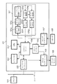
図1は第1の実施形態の構成を示したブロック図である。スキャナ106においてスキャンされた画像は、スキャナインタフェース107を介してマルチファンクションコントローラ111の内部に取り込まれる。取り込まれた画像が多値画像であればイメージプロセッサ110にて二値化し、二値画像であればそのままクロスバースイッチ104を介して、メインメモリ103に格納される。二値化された画像にOCR処理を施すためにCPU102はエッジ座標抽出回路101を起動し、ラスタ−ベクタ変換処理を開始する。エッジ座標抽出回路101が起動されると、リードDMAC101aがメインメモリ103から二値画像を取得し、データセレクタ101bへと送る。
【0024】
データセレクタ101bは、二値画像をバイト単位のストリームに変換してビットマップ−座標デコーダ101cへと送る。ビットマップ−座標デコーダ101cは入力された1バイトの二値画像が持つエッジ数と複数のエッジのx座標を並列にデコードし、その結果をデータ結合部101d(x座標データ結合回路)へ送る。データ結合部101dは、ビットマップ−座標デコーダ101cから受け取ったエッジのx座標をデータバッファに蓄積し、また当該ラインのエッジ数を積算する。データ結合部101dは、メモリへ転送可能な情報量だけエッジのx座標がデータバッファに蓄積された時点で、エッジのx座標のリストをx座標ライトDMAC101fへ転送し、x座標ライトDMAC101fは当該データをメインメモリ103の所定のアドレスへ格納する。
【0025】
ビットマップ−座標デコーダ101cはx方向のバイト数をカウントしており、ラインの終端まで到達した時点でラインの終了をデータ結合部101dへと報せる。ライン終了情報を受け取ったデータ結合部101dは、積算した当該ラインのエッジ数と、当該ラインの先頭のエッジ座標データを格納したアドレスの情報をデータ結合部101e(y座標データ結合回路)へと転送する。データ結合部101eはデータバッファにライン毎のエッジ数と格納アドレスを蓄積し、メモリ転送が可能となった時点でライン毎のエッジ数と格納アドレスをy座標ライトDMAC101gへ転送する。y座標ライトDMAC101gは更に当該データをメインメモリ103の所定のアドレスへ格納する。
【0026】
ビットマップ−座標デコーダ101cはy方向のライン数をカウントしており、二値画像の最終ラインの最終バイトまで到達した時点で、ラインの終了と共に処理の終了をデータ結合部101dへと報せる。処理終了情報を受け取ったデータ結合部101dは、データバッファに蓄積したx座標データをすべてx座標ライトDMAC101fに送ると共に、積算した当該ラインのエッジ数と、当該ラインの先頭のエッジ座標データを格納したアドレスの情報をデータ結合部101eへと、処理終了情報と共に転送する。終了情報を受け取ったデータ結合部101eは、データバッファに格納されたライン毎のエッジ数と格納アドレスを、y座標ライトDMAC101gへ転送し、y座標ライトDMAC101gは当該データをメインメモリ103の所定のアドレスへ格納し処理を終了する。
【0027】
エッジ座標抽出回路101が処理を開始し、2ライン分の処理が終了した時点から、CPU102はラスタ−ベクタ変換処理の後半処理をエッジ座標抽出回路101の処理とは並列に開始する。
【0028】
CPU102は、エッジ座標抽出回路101が出力したエッジ座標情報を元に、隣接したライン間の各エッジの関連性を調べ、ベクタを生成していく。エッジ座標抽出回路101とCPU102が処理を終了すると、二値画像がどのような輪郭を持った画像オブジェクトから成っているかが明らかになり、この情報を元にOCR処理を行う。OCR処理が行われるとスキャナ106でスキャンした画像がどのような方向を向いた文字を持っているかが判別できるため、この情報を元としてN-upのページ結合の処理を行い、結合されたページ画像がプリンタインタフェース109を介してプリンタエンジン108に送られ、プリントアウトされる。
【0029】
また、ホストコンピュータ100からネットワークインタフェース105を介してマルチファンクションコントローラ111にダウンロードされたビットマップフォントデータは、前述のラスタ−ベクタ処理を行う事により、描画オブジェクトとしてPDL描画処理に用いられる。
【0030】
図2は本実施の形態のエッジ座標抽出回路が生成するデータ形式を示した模式図である。元となる二値画像201を、エッジ座標抽出回路101にかけると、各ライン毎のエッジのx座標のリスト202が、x座標ライトDMAC101fによってメインメモリ103に書き込まれる。そして、同時に、各ライン毎のエッジ数203と、リスト202におけるライン先頭を示す行のアドレス(ポインタ)204とからなるリスト205が、y座標ライトDMAC101gによってメインメモリ103に書き込まれる。
【0031】
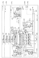
図3は本実施の形態のエッジ座標抽出回路101のデータパスを示したブロック図である。
【0032】
データリードDMAC101aがメモリから取得した二値画像データは、ビットマップレジスタ301に格納され、当該ビットマップデータはデータセレクタ302によってバイト単位に分割されてバイトレジスタ303に格納される。バイトレジスタ303に格納された8ビットのバイトデータは、インバータ317に送られる。インバータ317では、レジスタ316に格納された値に応じて、バイトデータを反転する。
【0033】
レジスタ316には1つ前(左側)のバイトのLSBが保持されている。この値が1であれば、バイトデータの右端の画素が濃度を有していることになる。従って、この場合には、トータルでのエッジ数が奇数になり、エッジでない座標がエッジと認識される可能性がある。そこで、エッジ位置及びエッジ数を調整するため、インバータ317において反転した上でビットマップ−座標デコーダ304に入力する。
【0034】
ビットマップ−座標デコーダ304には、8ビットのバイトデータが示す値と、エッジ位置情報及びエッジ数情報とを対応させて格納したルックアップテーブル(図4〜図9)が用意されており、バイトデータからエッジ位置情報及びエッジ数情報とに同時にデコードする。
【0035】
例えば、図2においては、0行目の最初のバイトデータは、16進数で03であり、LSBは1である。従って、レジスタ316は、この値1を次のバイトデータがバイトレジスタ303から出力されるまで保持している。続くバイトデータは、16進数で80であり、これがレジスタ303に保持されると、インバータ317は、レジスタ316が1であるから、80を7fに変換する。これにより、エッジデコーダ304はエッジ数1、エッジ位置1を出力することになり、連続するバイトデータ間で適正に調整が行われる。
【0036】
ビットマップ−座標デコーダ304によってデコードされた、バイトデータ内に含まれるエッジ数と全てのエッジの位置の座標情報は、エッジ数レジスタ306と下位エッジx座標レジスタ305に格納される。ビットマップ−座標デコーダ101cはx方向のバイトカウンタ307を持っており、これがエッジの上位x座標となる。
【0037】
下位エッジx座標レジスタ305はバレルシフタ311によってシフトされ上位x座標カウンタ307の出力とビット結合されてx座標データ結合レジスタ312に格納される。
【0038】
バイト内のエッジ数はエッジ数カウンタ313に入力され、ライン内のエッジ数をカウントするのに用いられる。ライン内エッジ数の下位ビットと現在バイトのエッジ数であるエッジ数レジスタ306の出力がデコーダ314に入力され、バレルシフタ311のシフト量と、x座標データ結合レジスタ312のロード信号が生成される。
【0039】
このバレルシフタ311の動作について、図2(a)の画像を例にとり説明する。0ライン目の最初のバイトは16進数で03である。デコーダ304によってエッジ位置がデコードされ、図4においてバイトデータ(byte data)が3の行に示すように、エッジ位置情報(edge position)として値"6,0,0,0,0,0,0,0"が下位エッジx座標レジスタ305へ格納される。最初のバイトであるため、デコーダ314が出力するデコード量は0であるから、最初のエッジ位置である6が、上位x座標カウンタ307の値0と結合されて、エッジ位置が6となり、左端のレジスタ312に保持される。
【0040】
0ライン目の続くバイトは80であるが、前バイトのLSBビットが1であったために、インバータ317によって7fに変換され、デコーダ304によって、値"1,0,0,0,0,0,0,0"が下位エッジx座標レジスタ305に格納される。0ライン目の積算エッジ数が最初のバイトで1になっていたため、デコーダ314が1セグメントのシフトをバレルシフタ311に指示し、左から4つの値をレジスタ312に出力する。つまり、値"1,0,0,0,0,0,0,0"は値"0,1,0,0"となってバレルシフタ311から出力される。
【0041】
上位x座標カウンタ307は最初のバイトの処理によって1にカウントアップされているため、バレルシフタの出力"0,1,0,0"の1と結合されて二進数1001、十進で9の値がレジスタ312の左から2番目のレジスタに格納される。これにより図2の204の最初の行に相当する"6,9"の値が生成される。
【0042】
図2では説明を容易にするために1ライン16画素の画像を表したが、ここで示されるエッジ座標抽出回路101は、より現実的に、1ラインが232画素で構成される画像を扱うものである。従って、最終的にレジスタ312には、32ビットのエッジ座標が格納される。
【0043】
x座標データ結合レジスタ312が満杯になると、結合された座標データはx座標ライトDMAC101fに送られ、エッジ座標データ204としてメインメモリ103に格納される。エッジ座標データ204の格納アドレスはアドレスカウンタ315によってカウントされ、ラインの先頭のアドレスはデータ結合部101eに送られる。
【0044】
また、1回の出力でバレルシフタ311からレジスタ312に出力できない場合には、満杯になったレジスタ312からライトDMAC101fに座標データが送られた後に、バレルシフタ311に残った値を適宜シフトしてレジスタ312に送る。
【0045】
ビットマップ−座標デコーダ101cは上位x座標カウンタ307の値とラインの長さのバイト数をライン終了比較器308によって比較しており、上位x座標カウンタ307の値がライン終了まで達したところでライン終了信号がライン終了レジスタ309に保持される。ライン終了情報が発生すると、アドレスカウンタ315の値とラインエッジ数カウンタ313の値がy座標データ結合回路101eへ送られる。ビットマップ−座標デコーダ101cはまたy方向のラインカウンタ310を持っており、ライン終了レジスタ309の情報をカウントしつつ、ビットマップ画像の総ライン数と比較している。ライン数が最終に達すると処理終了信号を発生し、ライトDMAC101f,101gに保持したデータ全てをメモリ103へ書き出すように指示し、全体の処理を終了させる。
【0046】
図4〜図9は本実施の形態のビットマップ−座標デコーダ304の入出力を示した真理値表である。本実施の形態はMSB側がビットマップの左端としており、0が白、1が黒、背景が白としているため、例えばバイトレジスタ303の出力が0x06の場合には、エッジ数の出力が2、第1エッジの位置(下位x座標)が5、第2エッジの位置(下位x座標)が7をデコードし、第3エッジ以降の値に無効を示す0がデコードされ、これらのデータがエッジ数レジスタ306、下位x座標レジスタ311へと格納される。
【0047】
なお、図4〜図9で示したテーブルは、あくまで例示的なものに過ぎず、バイトデータの値とエッジ座標情報及びエッジ数情報とを対応させて格納したテーブルであれば、如何なるテーブルも本発明に適用することができる。
【0048】
以上説明したように、本実施形態によれば、ラスタ−ベクタ処理の前半部分に当たるエッジ抽出処理を高速に行うことが可能となり、さらにエッジ同士の関連を導出してベクタ変換する処理をCPU上のソフトウェアで並列に行うことによって、ラスタ−ベクタ処理を短時間に行うことが可能となる。
【0049】
(第2の実施形態)
既に述べたように、特開2000-137825号公報において、描画オブジェクトの輪郭情報と、描画オブジェクトの上下関係をあらわすレイヤー情報から、直接最終ピクセルを生成する、レンダリングの方法が、提案されている。
【0050】
この方法は、オブジェクトの輪郭情報からどのオブジェクトが存在するかを判断し、つづいてオブジェクトの上下関係からどのオブジェクトが表面に存在するからを判断し、最後に表面に存在するオブジェクトの色情報から、現在注目しているピクセルがどの色かを判断することで、ピクセルを生成することを、1ピクセル毎に行う。そのため、レンダリング時にメモリへのリード・モディファイ・ライトを多量に行う必要がなく、解像度や諧調が増えても、レンダリング時間が飛躍的に長くなることはない。
【0051】
この方法では、レンダリング処理前に、あらかじめオブジェクトの輪郭情報を得ておく必要がある。通常プリントする文章では文字が多く含まれるが、文字のフォントオブジェクトに対しても輪郭情報を得ておく必要がある。
【0052】
本実施の形態では、ビットマップ−エッジ座標変換を行うデコーダを用いたエッジ座標抽出回路を構成し、輪郭情報の抽出処理の前半を高速化する。更に、処理の後半をCPU上のソフトウェアで実行する際に、処理の前半とオーバラップさせて並列処理を行う事により、輪郭情報の抽出処理を短期間に行う。
【0053】
<構成>
図10は第2の実施形態の構成を示したブロック図である。ホストコンピュータ1000によって生成されたプリント情報が、ネットワークを解してマルチファンクションコントローラ1011へと送られる。ネットワークインターフェース1005によって受信されたプリント情報は、クロスバースイッチ1004を介して一度メインメモリ1003へ格納される。続いてCPU1002はメインメモリ1003へ格納されたプリント情報の解析を開始し、描画オブジェクトの輪郭情報、レイヤー情報、色情報等を、ディスプレイリストとしてメインメモリ1003の別の領域に生成していく。描画オブジェクトが文字であった場合には、フォントキャッシュを検索し、キャッシュヒットした場合にはフォントキャッシュ内に登録されている輪郭情報をディスプレイリストに追加し、キャッシュミスした場合にはビットマップフォントメインメモリ1003の別の領域に生成し、続く輪郭情報抽出処理に移行する。
【0054】
ビットマップフォントの輪郭情報を抽出するために、まずCPU1002はエッジ座標抽出回路1001にビットマップフォントが格納されたメモリアドレスを与え、これを起動する。エッジ座標抽出回路1001が起動されると、リードDMAC1001aがメインメモリ1003より、前出のビットマップフォント画像を取得し、データセレクタ1001bへと送る。
【0055】
データセレクタ1001bは、ビットマップフォント画像をバイト単位のストリームに変換してビットマップ−座標デコーダ1001cへと送る。ビットマップ−座標デコーダ1001cは入力された1バイトのビットマップ画像が持つエッジ数と複数のエッジのx座標を並列にデコードし、その結果をデータ結合部1001d(x座標データ結合回路)へ送る。データ結合部1001dはビットマップ−座標デコーダ1001cから受け取ったエッジのx座標をデータバッファに蓄積し、また当該ラインのエッジ数を積算する。データ結合部1001dは、メモリへ転送可能な情報量だけエッジのx座標がデータバッファに蓄積された時点で、エッジのx座標のリストをx座標ライトDMAC101fへ転送し、x座標ライトDMAC1001fは当該データをメインメモリ1003の所定のアドレスへ格納する。
【0056】
ビットマップ−座標デコーダ1001cはx方向のバイト数をカウントしており、ラインの終端まで到達した時点でラインの終了をデータ結合部1001dへと報せる。ライン終了情報を受け取ったデータ結合部1001dは、積算した当該ラインのエッジ数と、当該ラインの先頭のエッジ座標データを格納したアドレスの情報をデータ結部1001e(y座標データ結合回路)へと転送する。データ結合部1001eはデータバッファにライン毎のエッジ数と格納アドレスを蓄積し、メモリ転送が可能となった時点でライン毎のエッジ数と格納アドレスをy座標ライトDMAC1001gへ転送する。y座標ライトDMAC1001gは更に当該データをメインメモリ1003の所定のアドレスへ格納する。
【0057】
ビットマップ−座標デコーダ1001cはy方向のライン数をカウントしており、ビットマップ画像の最終ラインの最終バイトまで到達した時点で、ラインの終了と共に処理の終了をデータ結合部1001dへと報せる。処理終了情報を受け取ったデータ結合部1001dは、データバッファに蓄積したx座標データをすべてx座標ライトDMAC1001fに送ると共に、積算した当該ラインのエッジ数と、当該ラインの先頭のエッジ座標データを格納したアドレスの情報をデータ結合部1001eへと、処理終了情報と共に転送する。終了情報を受け取ったデータ結合部1001eは、データバッファに格納されたライン毎のエッジ数と格納アドレスを、y座標ライトDMAC1001gへ転送し、y座標ライトDMAC1001gは当該データをメインメモリ1003の所定のアドレスへ格納し処理を終了する。
【0058】
エッジ座標抽出回路1001が処理を開始し、2ライン分の処理が終了した時点から、CPU1002はエッジ座標から輪郭情報を抽出する処理をエッジ座標抽出回路1001の処理とは並列に開始する。
【0059】
CPU1002はエッジ座標抽出回路1001が出力したエッジ座標情報を元に、隣接したライン間の各エッジの関連性を調べ、ベクタを生成していく。エッジ座標抽出回路1001とCPU1002が処理を終了すると、ビットマップフォントの輪郭情報が得られる。CPU1002はこの輪郭情報をフォントキャッシュに登録するとともに、ディスプレイリストへも登録する。
【0060】
こうして1ページ分のディスプレイリストが生成されると、CPU1002はこのディスプレイリストを元にレンダリング処理を行い、プリントすべき画像をメインメモリ1003へ生成する。生成された画像はクロスバースイッチ1004、画像処理回路1010を介してプリンタインターフェース1009より、プリントエンジン1008へと送られる。プリントエンジン1008では、受信した画像を記録媒体である紙に記録し、最終的なプリントアウトが得られる。
【0061】
図11は本実施の形態のエッジ座標抽出回路が生成するデータ形式を示した模式図である。元となるビットマップ画像1101を、エッジ座標抽出回路1001にかけると、各ライン毎のエッジのx座標のリスト1102が、x座標ライトDMAC1001fによってメインメモリ1003に書き込まれる。そして、同時に、各ライン毎のエッジ数1103と、リスト1102におけるライン先頭を示す行のアドレス(ポインタ)1104とからなるリスト1105が、y座標ライトDMAC1001gによってメインメモリ1003に書き込まれる。
【0062】
図12は本実施の形態のエッジ座標抽出回路1001のデータパスを示したブロック図である。
【0063】
データリードDMAC101aがメモリから取得したビットマップ画像データは、ビットマップレジスタ1201に格納され、当該ビットマップデータはデータセレクタ1202によってバイト単位に分割されてバイトレジスタ1203に格納される。バイトレジスタ1203に格納されたビットマップデータは、インバータ1217に送られる。インバータ1217では、レジスタ1216に格納された値に応じて、バイトデータを反転する。
【0064】
レジスタ1216には1つ前(左側)のバイトのLSBが保持されている。この値が1であれば、バイトデータの右端の画素が濃度を有していることになる。従って、この場合には、トータルでのエッジ数が奇数になり、エッジでない座標がエッジと認識される可能性がある。そこで、エッジ位置及びエッジ数を調整するため、インバータ1217において反転した上でビットマップ−座標デコーダ1204に入力する。
【0065】
ビットマップ−座標デコーダ1204には、8ビットのバイトデータが示す値と、エッジ位置情報及びエッジ数情報とを対応させて格納したルックアップテーブル(図4〜図9)が用意されており、バイトデータからエッジ位置情報及びエッジ数情報とに同時にデコードする。
【0066】
ビットマップ−座標デコーダ1204によってデコードされた、バイトデータ内に含まれるエッジ数と全てのエッジの位置の座標情報は、エッジ数レジスタ1206と下位エッジx座標レジスタ1205に格納される。ビットマップ−座標デコーダ1001cはx方向のバイトカウンタ1207を持っており、これがエッジの上位x座標となる。
【0067】
下位エッジx座標レジスタ1205はバレルシフタ1211によってシフトされ上位x座標カウンタ1207の出力とビット結合されてx座標データ結合レジスタ1212に格納される。
【0068】
バイト内のエッジ数はエッジ数カウンタ1213に入力され、ライン内のエッジ数がカウントするのに用いられる。ライン内エッジ数の下位ビットと現在バイトのエッジ数であるエッジ数レジスタ1206の出力がデコーダ1214に入力され、バレルシフタ1211のシフト量と、x座標データ結合レジスタ1212のロード信号が生成される。
【0069】
このバレルシフタ1211の動作は、第1の実施形態において、図2(a)の画像を例に説明したものと同様であるので、その詳細な説明は省略する。
【0070】
x座標データ結合レジスタ1212が満杯になると、結合された座標データはx座標ライトDMAC1001fに送られ、エッジ座標データ1104としてメインメモリ1003に格納される。エッジ座標データ1104の格納アドレスはアドレスカウンタ1215によってカウントされ、ラインの先頭のアドレスはデータ結合部1001eに送られる。
【0071】
また、1回の出力でバレルシフタ1211からレジスタ1212に出力できない場合には、満杯になったレジスタ1212からライトDMAC1001fに座標データが送られた後に、バレルシフタ1211に残った値を適宜シフトしてレジスタ1212に送る。
【0072】
ビットマップ−座標デコーダ1001cは上位x座標カウンタ1207の値とラインの長さのバイト数をライン終了比較器1208によって比較しており、上位x座標カウンタ1207の値がライン終了まで達したところでライン終了信号がライン終了レジスタ1209に保持される。ライン終了情報が発生すると、アドレスカウンタ1215の値とラインエッジ数カウンタ1213の値がy座標データ結合回路1001eへ送られる。ビットマップ−座標デコーダ1001cはまたy方向のラインカウンタ1210を持っており、ライン終了レジスタ1209の情報をカウントしつつ、ビットマップ画像の総ライン数と比較している。ライン数が最終に達すると処理終了信号を発生し、ライトDMAC1001f, 1001gに保持したデータ全てをメモリ1003へ書き出すように指示し、全体の処理を終了させる。
【0073】
<ソフトウェア処理>
図13は本実施の形態の輪郭抽出処理のソフトウェアシーケンスを示したフローチャートである。なお本フローチャートの処理は、メインメモリ1003に予め格納されているプログラムに基づき、CPU1002が実行する。
【0074】
はじめに、エッジ座標抽出回路1001が生成するエッジ情報を格納するメモリ領域を確保し(S1301)、続いてエッジ座標抽出回路1001に必要なビットマップフォントが格納されたアドレス等のパラメータを設定し(S1302)、エッジ座標抽出回路1001を起動してエッジ座標抽出処理を開始する(S1303)。
【0075】
次にエッジ座標抽出回路1001が2ライン以上の処理を終えたかを判断し(S1304)、まだ処理を終えていなければ2ライン以上の処理を終えるまで待ち、2ライン以上の処理を終えていれば、注目ラインを2ライン目に指定し、エッジ座標抽出処理と並列にエッジ座標から輪郭情報を生成する処理を開始する(S1305)。
【0076】
エッジ座標から輪郭情報を生成する処理は、注目エッジの初期値が主走査の原点方向にあることを前提に、まず注目ラインの未処理エッジ数が0かを判断する(S1306)。
【0077】
ステップS1306において、未処理エッジ数が0よりも大きい場合には、注目エッジが前ラインから注目ラインへ移った際の傾きを計算し、輪郭情報に付加する(S1307)。次に注目エッジを主走査方向に進め(S1308)、ステップS1306に戻り、再度未処理エッジ数が0かを判断する。
【0078】
ステップS1306において、未処理エッジ数が0で合った場合には、つぎに注目ラインを1進め、注目エッジを主走査原点方向に戻す(S1309)。次にビットマップすべてのラインに対して処理を行ったか、すなわち、残りライン数が0であるかを判断し(S1310)、ラインが残っている場合には次にエッジ抽出回路1001が注目ラインの処理を終えているかを判断し(S1311)、注目ラインの処理を終えていない場合には処理が進むのを待ち、注目ラインの処理が終えている場合には、ステップS1306に戻り、また未処理エッジ数の判断を行う。もしビットマップフォントのすべてのラインに対して処理を終えたならば、処理は終了である。
【0079】
本実施形態において、ビットマップ−座標デコーダ1204の入出力を示した真理値表は、第1の実施形態で示した図4〜9の真理値表と同一である。本実施の形態はMSB側がビットマップの左端としており、0が白、1が黒、背景が白としているため、例えばバイトレジスタ1203の出力が0x06の場合には、エッジ数の出力が2、第1エッジの位置(下位x座標)が5、第2エッジの位置(下位x座標)が7をデコードし、第3エッジ以降の値に無効を示す0がデコードされ、これらのデータがエッジ数レジスタ1206、下位x座標レジスタ1203へと格納される。
【0080】
なお、本実施形態では、第1の実施形態と同様に、図4〜図9で示したテーブルを用いたが、これらは、あくまで例示的なものに過ぎず、レンダリング処理のために別途設定した専用のテーブルを適用してもよい。
【0081】
以上説明したように、本実施形態によれば、オブジェクトの輪郭情報生成処理の前半部分にあたるエッジ抽出処理を高速に行うことが可能となり、さらにエッジ同士の関連を導出して輪郭情報を生成する処理をCPU上のソフトウェアで並列に行うことによって、オブジェクトの輪郭情報生成処理を短時間に行うことが可能となる。
【0082】
特に、文字が多く含まれる文書のレンダリングを行う場合においても、フォントオブジェクト単位で高速な輪郭抽出処理ができるので、高速なプリント処理が実行可能となる。
【0083】
【発明の効果】
本発明によれば、エッジ抽出処理を高速に行うことのできる画像処理装置及び画像処理方法を提供することができる。
【図面の簡単な説明】
【図1】本発明の第1の実施形態の構成を示したブロック図である。
【図2】本発明の第1の実施形態のエッジ座標抽出回路が生成するデータ形式を示した模式図である。
【図3】本発明の第1の実施形態のエッジ座標抽出回路のデータパスを示したブロック図である。
【図4】本発明の実施形態のデコーダ回路の動作の真理値表を示す図である。
【図5】本発明の実施形態のデコーダ回路の動作の真理値表を示す図である。
【図6】本発明の実施形態のデコーダ回路の動作の真理値表を示す図である。
【図7】本発明の実施形態のデコーダ回路の動作の真理値表を示す図である。
【図8】本発明の実施形態のデコーダ回路の動作の真理値表を示す図である。
【図9】本発明の実施形態のデコーダ回路の動作の真理値表を示す図である。
【図10】本発明の第2の実施形態の構成を示したブロック図である。
【図11】本発明の第2の実施形態のエッジ座標抽出回路が生成するデータ形式を示した模式図である。
【図12】本発明の第2の実施形態のエッジ座標抽出回路のデータパスを示したブロック図である。
【図13】本発明の第2の実施形態の輪郭抽出処理のソフトウェアシーケンスを示したフローチャートである。
【符号の説明】
101 : エッジ座標抽出回路
101a : リードDMAC
101b : データセレクタ
101c : ビットマップ−座標デコーダ
101d : x座標データ結合回路
101e : y座標データ結合回路
101f : x座標データライトDMAC
101g : y座標データライトDMAC
102 : CPU
103 : メモリ
104 : クロスバー回路
105 : ネットワークインタフェース
106 : スキャナ
107 : スキャナインタフェース
108 : プリンタ
109 : プリンタインタフェース
110 : イメージ処理回路
111 : マルチファンクションコントローラ
201 : ビットマップ画像
202 : エッジのx座標
203 : ライン内のエッジ数
204 : ラインの先頭へのポインタ
301 : ビットマップデータバッファ
302 : バイトセレクタ
303 : バイトバッファ
304 : ビットマップ−座標デコーダ
305 : 下位 x 座標レジスタ
306 : エッジ数レジスタ
307 : 上位 x 座標カウンタ
308 : ライン終了比較器
309 : ライン終了フラグレジスタ
310 : ライン数カウンタ
311 : バレルシフタ
312 : x座標データ結合レジスタ
313 : ラインエッジ数カウンタ
314 : デコーダ
315 : アドレスカウンタ[0001]
BACKGROUND OF THE INVENTION
The present invention relates to an image processing apparatus and an image processing method for processing an input bitmap image.
[0002]
[Prior art]
Conventionally, printers and multi-function peripheral systems that process page description languages (PDL) such as PostScript, LIPS, and PCL have a frame buffer such as a band buffer or a page buffer, and a process of rendering a drawing object in the frame buffer is performed. It was. In this case, an image around the drawing object is read from the frame buffer, combined with the drawing object, and written back to the frame buffer for all the drawing objects. For this reason, it has been necessary to perform a large amount of read-modify-write processing on the memory serving as the frame buffer. Therefore, when the resolution of the printer is high or when the color printer outputs with high gradation, there has been a problem that the rendering time becomes very long. In order to solve this problem, Japanese Patent Laid-Open No. 2000-137825 proposes a rendering method in which the final pixel is directly generated from the outline information of the drawing object and the layer information representing the vertical relationship of the drawing object. This method recognizes an object existing at a certain pixel position from the contour information of the object, and then determines which object is present in the uppermost layer from the hierarchical relationship of those objects, and finally exists in the uppermost layer. Pixel data is generated for each pixel by determining which color is the pixel of interest from the color information of the object. Therefore, it is not necessary to perform a large amount of read-modify-write to the memory at the time of rendering, and even if the resolution and gradation increase, the rendering time does not become so long.
[0003]
[Problems to be solved by the invention]
However, in the above prior art, before rendering a certain page, it is necessary to obtain outline information of an object existing on the page in advance. If the page contains many characters, it is necessary to obtain outline information about the font object of the characters. However, since there are many types of characters and the contour is complicated, there arises a problem that it takes time for the contour extraction processing.
[0004]
In addition, a normal bitmap font is a binary bitmap image, and the process of extracting the contour from the binary bitmap image is a bit operation, and therefore a process that requires a large number of cycles to be processed by a normal CPU. Thus, there is a problem that it is difficult to process at high speed.
[0005]
Further, the problem related to the contour extraction process is not limited to the rendering process but also occurs when the raster-vector process in the OCR process is executed.
[0006]
That is, when performing OCR on an image scanned from a scanner, raster-vector processing is performed. In the first half of the raster-vector processing, each pixel of the raster image is searched and the coordinates of the density change point (edge) are obtained. In the second half of the processing, the relationship between the edges is inferred from the edge coordinates. Generate a vector. Conventionally, all the raster-vector processing including the processing for obtaining the coordinates has been performed by software processing by the CPU.
[0007]
In OCR, a raster image to be processed is often a binary bitmap image. In the process of searching for each pixel of the binary bitmap image, it is necessary to perform a large amount of bit operations, and a normal CPU consumes many cycles for bit operations. As a result, a problem arises that in software processing, raster-vector processing takes a long time.
[0008]
SUMMARY An advantage of some aspects of the invention is that it provides an image processing apparatus and an image processing method capable of performing raster-vector processing at high speed.
[0009]
In order to achieve the above object, in the apparatus according to the present invention, an edge coordinate extraction circuit that extracts edge coordinate information from a bitmap image in line order, and the edge coordinate extraction circuit execute the computer program to execute extraction. Conversion means for converting the bitmap image into vector data based on the edge coordinate information that has been converted, and the conversion to the vector data by the conversion means is a software process, and the edge coordinates by the edge coordinate extraction circuit The information extraction is a hardware process, and the conversion process to the vector data by the conversion unit is started when the edge coordinate information extraction process by the edge coordinate extraction circuit is completed for two lines of the bitmap image. And then performing the extraction process and the conversion process in parallel. That.
[0010]
To achieve the above object, the method according to the present invention is an image processing method for processing a bitmap image, wherein an edge coordinate extraction circuit extracts edge coordinate information from the bitmap image in line order. A coordinate extraction step; and a conversion step of converting the bitmap image into vector data based on the edge coordinate information extracted in the edge coordinate extraction step by causing the CPU to execute a computer program, When the extraction processing of the edge coordinate information by the edge coordinate extraction circuit is completed for two lines of the bitmap image, the CPU starts the conversion processing to the vector data, and then the extraction processing and the conversion processing Are executed in parallel.
[0021]
DETAILED DESCRIPTION OF THE INVENTION
Embodiments of the present invention will be described below with reference to the drawings.
[0022]
(First embodiment)
In the present embodiment, an edge coordinate extraction circuit using a decoder that performs bitmap-edge coordinate conversion is configured to speed up the first half of raster-vector processing. Further, when the second half of the processing is executed by software on the CPU, the raster-vector processing is performed in a short time by overlapping the first half of the processing and performing parallel processing.
[0023]
<Configuration>
FIG. 1 is a block diagram showing the configuration of the first embodiment. An image scanned by the
[0024]
The
[0025]
The bitmap-coordinate
[0026]
The bitmap-coordinate
[0027]
The
[0028]
Based on the edge coordinate information output from the edge coordinate
[0029]
The bitmap font data downloaded from the
[0030]
FIG. 2 is a schematic diagram showing a data format generated by the edge coordinate extraction circuit of the present embodiment. When the original
[0031]
FIG. 3 is a block diagram showing a data path of the edge coordinate
[0032]
The binary image data acquired from the memory by the data read
[0033]
The
[0034]
The bitmap-coordinate
[0035]
For example, in FIG. 2, the first byte data of the 0th row is 03 in hexadecimal and LSB is 1. Therefore, the
[0036]
The number of edges included in the byte data and the coordinate information of the positions of all edges decoded by the bitmap-coordinate
[0037]
The lower
[0038]
The number of edges in the byte is input to an
[0039]
The operation of the
[0040]
The succeeding byte of the 0th line is 80, but since the LSB bit of the previous byte is 1, it is converted to 7f by the
[0041]
Since the upper
[0042]
In FIG. 2, an image of 16 pixels per line is shown for ease of explanation, but the edge coordinate
[0043]
When the x-coordinate data combination register 312 becomes full, the combined coordinate data is sent to the x-coordinate
[0044]
If the
[0045]
The bitmap-coordinate
[0046]
4 to 9 are truth tables showing input / output of the bitmap-coordinate
[0047]
Note that the tables shown in FIGS. 4 to 9 are merely illustrative, and any table can be used as long as the table stores byte data values in association with edge coordinate information and edge number information. It can be applied to the invention.
[0048]
As described above, according to the present embodiment, the edge extraction processing corresponding to the first half of the raster-vector processing can be performed at high speed, and the processing for deriving the relationship between the edges and performing vector conversion is performed on the CPU. By performing in parallel with software, raster-vector processing can be performed in a short time.
[0049]
(Second Embodiment)
As already described, Japanese Patent Application Laid-Open No. 2000-137825 proposes a rendering method that directly generates the final pixel from the outline information of the drawing object and the layer information representing the vertical relationship of the drawing object.
[0050]
This method determines which object exists from the contour information of the object, then determines which object exists on the surface from the hierarchical relationship of the object, and finally from the color information of the object present on the surface, A pixel is generated for each pixel by determining which color the pixel currently focused on is. Therefore, it is not necessary to perform a large amount of read-modify-write to the memory at the time of rendering, and even if the resolution and gradation increase, the rendering time does not increase dramatically.
[0051]
In this method, it is necessary to obtain outline information of the object in advance before rendering processing. Normally, text to be printed contains many characters, but it is necessary to obtain outline information for the font object of the characters.
[0052]
In this embodiment, an edge coordinate extraction circuit using a decoder that performs bitmap-edge coordinate conversion is configured to speed up the first half of the contour information extraction processing. Further, when the second half of the processing is executed by software on the CPU, the parallel processing is performed by overlapping with the first half of the processing, so that the contour information extraction processing is performed in a short time.
[0053]
<Configuration>
FIG. 10 is a block diagram showing the configuration of the second embodiment. Print information generated by the
[0054]
In order to extract the outline information of the bitmap font, first, the
[0055]
The
[0056]
The bitmap-coordinate
[0057]
The bitmap-coordinate
[0058]
When the edge coordinate
[0059]
Based on the edge coordinate information output from the edge coordinate
[0060]
When the display list for one page is generated in this way, the
[0061]
FIG. 11 is a schematic diagram showing a data format generated by the edge coordinate extraction circuit of the present embodiment. When the
[0062]
FIG. 12 is a block diagram showing a data path of the edge coordinate
[0063]
The bitmap image data acquired from the memory by the data read
[0064]
The
[0065]
The bitmap-coordinate decoder 1204 is provided with a look-up table (FIGS. 4 to 9) that stores a value indicated by 8-bit byte data in association with edge position information and edge number information. Data is simultaneously decoded into edge position information and edge number information.
[0066]
The number of edges included in the byte data and the coordinate information of all edge positions decoded by the bitmap-coordinate decoder 1204 are stored in the
[0067]
The lower
[0068]
The number of edges in the byte is input to an
[0069]
Since the operation of the
[0070]
When the x-coordinate
[0071]
If the
[0072]
The bitmap-coordinate
[0073]
<Software processing>
FIG. 13 is a flowchart showing a software sequence for contour extraction processing according to the present embodiment. Note that the processing of this flowchart is executed by the
[0074]
First, a memory area for storing edge information generated by the edge coordinate
[0075]
Next, it is determined whether or not the edge coordinate
[0076]
In the process of generating the contour information from the edge coordinates, it is first determined whether or not the number of unprocessed edges of the target line is 0 on the assumption that the initial value of the target edge is in the main scanning origin direction (S1306).
[0077]
If the number of unprocessed edges is larger than 0 in step S1306, the inclination when the edge of interest moves from the previous line to the line of interest is calculated and added to the contour information (S1307). Next, the target edge is advanced in the main scanning direction (S1308), and the process returns to step S1306 to determine again whether the number of unprocessed edges is zero.
[0078]
In step S1306, if the number of unprocessed edges is 0, the target line is advanced by 1 and the target edge is returned to the main scanning origin direction (S1309). Next, it is determined whether processing has been performed for all the lines of the bitmap, that is, whether the number of remaining lines is 0 (S1310). If there are remaining lines, the
[0079]
In this embodiment, the truth table showing the input / output of the bitmap-coordinate decoder 1204 is the same as the truth table of FIGS. 4 to 9 shown in the first embodiment. In this embodiment, since the MSB side is the left end of the bitmap, 0 is white, 1 is black, and the background is white. For example, when the output of the
[0080]
In this embodiment, as in the first embodiment, the tables shown in FIGS. 4 to 9 are used. However, these are merely illustrative and are set separately for rendering processing. A dedicated table may be applied.
[0081]
As described above, according to the present embodiment, the edge extraction process corresponding to the first half of the contour information generation process of the object can be performed at high speed, and the process of generating the contour information by deriving the relationship between the edges. Are performed in parallel by software on the CPU, the object contour information generation processing can be performed in a short time.
[0082]
In particular, even when rendering a document containing many characters, a high-speed contour extraction process can be performed for each font object, so that a high-speed print process can be executed.
[0083]
【The invention's effect】
ADVANTAGE OF THE INVENTION According to this invention, the image processing apparatus and image processing method which can perform an edge extraction process at high speed can be provided.
[Brief description of the drawings]
FIG. 1 is a block diagram showing a configuration of a first exemplary embodiment of the present invention.
FIG. 2 is a schematic diagram showing a data format generated by an edge coordinate extraction circuit according to the first embodiment of the present invention.
FIG. 3 is a block diagram showing a data path of the edge coordinate extraction circuit according to the first embodiment of the present invention.
FIG. 4 is a diagram showing a truth table of the operation of the decoder circuit according to the embodiment of the present invention.
FIG. 5 is a diagram showing a truth table of the operation of the decoder circuit according to the embodiment of the present invention.
FIG. 6 is a diagram showing a truth table of the operation of the decoder circuit according to the embodiment of the present invention.
FIG. 7 is a diagram showing a truth table of the operation of the decoder circuit according to the embodiment of the present invention.
FIG. 8 is a diagram showing a truth table of the operation of the decoder circuit according to the embodiment of the present invention;
FIG. 9 is a diagram showing a truth table of the operation of the decoder circuit according to the embodiment of the present invention.
FIG. 10 is a block diagram showing a configuration of a second exemplary embodiment of the present invention.
FIG. 11 is a schematic diagram showing a data format generated by an edge coordinate extraction circuit according to the second embodiment of the present invention.
FIG. 12 is a block diagram illustrating a data path of an edge coordinate extraction circuit according to a second embodiment of this invention.
FIG. 13 is a flowchart showing a software sequence of contour extraction processing according to the second embodiment of the present invention.
[Explanation of symbols]
101: Edge coordinate extraction circuit
101a: Read DMAC
101b: Data selector
101c: Bitmap-coordinate decoder
101d: x-coordinate data combination circuit
101e: y-coordinate data combination circuit
101f: x coordinate data write DMAC
101g: y coordinate data write DMAC
102: CPU
103: Memory
104: Crossbar circuit
105: Network interface
106: Scanner
107: Scanner interface
108: Printer
109: Printer interface
110: Image processing circuit
111: Multi-function controller
201: Bitmap image
202: x coordinate of the edge
203: Number of edges in the line
204: Pointer to the beginning of the line
301: Bitmap data buffer
302: Byte selector
303: Byte buffer
304: Bitmap-coordinate decoder
305: Lower x coordinate register
306: Edge number register
307: Upper x coordinate counter
308: Line end comparator
309: Line end flag register
310: Line number counter
311: Barrel shifter
312: x-coordinate data combination register
313: Line edge number counter
314: Decoder
315: Address counter
Claims (8)
コンピュータプログラムを実行することにより、前記エッジ座標抽出回路で抽出されたエッジ座標情報に基づき、前記ビットマップ画像をベクタデータに変換する変換手段と、
を含み、
前記変換手段による前記ベクタデータへの変換はソフトウェア処理であり、前記エッジ座標抽出回路による前記エッジ座標情報の抽出はハードウェア処理であり、
前記エッジ座標抽出回路による前記エッジ座標情報の抽出処理が前記ビットマップ画像の2ライン分終了した時点から、前記変換手段による前記ベクタデータへの変換処理を開始し、その後、前記抽出処理と前記変換処理とを並列に実行することを特徴とする画像処理装置。An edge coordinate extraction circuit that extracts edge coordinate information from the bitmap image in line order ; and
Conversion means for converting the bitmap image into vector data based on the edge coordinate information extracted by the edge coordinate extraction circuit by executing a computer program;
Only including,
Conversion to the vector data by the conversion means is software processing, extraction of the edge coordinate information by the edge coordinate extraction circuit is hardware processing,
When the edge coordinate information extraction processing by the edge coordinate extraction circuit is completed for two lines of the bitmap image, the conversion means starts conversion processing to the vector data, and then the extraction processing and the conversion An image processing apparatus that executes processing in parallel .
前記エッジ座標抽出回路は、前記二値ビットマップ画像のエッジ座標情報を抽出し、
前記変換手段は、前記コンピュータプログラムを実行することにより、前記エッジ座標抽出回路で抽出されたエッジ座標情報に基づき、前記二値ビットマップ画像をベクタデータに変換することを特徴とする請求項1記載の画像処理装置。The bitmap image is a binary bitmap image;
The edge coordinate extraction circuit extracts edge coordinate information of the binary bitmap image;
2. The conversion means converts the binary bitmap image into vector data based on edge coordinate information extracted by the edge coordinate extraction circuit by executing the computer program. Image processing apparatus.
前記ビットマップ画像から、連続するnビットのデータを抽出する抽出手段と、
前記抽出手段により抽出されたnビットデータから、エッジ位置情報及びエッジ数情報を同時にデコードするデコード手段と、
前記デコード手段によって導き出した、前記nビットデータ毎のエッジ位置情報及びエッジ数情報を結合して、1ライン毎のエッジ位置情報及びエッジ数情報を導き出すデータ結合手段と、
を有することを特徴とする請求項1に記載の画像処理装置。The edge coordinate extraction circuit includes:
Extraction means for extracting continuous n-bit data from the bitmap image;
Decoding means for simultaneously decoding edge position information and edge number information from the n-bit data extracted by the extracting means;
Data combining means for deriving edge position information and edge number information for each line by combining edge position information and edge number information for each of the n-bit data derived by the decoding means;
The image processing apparatus according to claim 1 , further comprising:
エッジ座標抽出回路が、前記ビットマップ画像からエッジ座標情報をライン順に抽出するエッジ座標抽出工程と、
CPUにコンピュータプログラムを実行させることにより、CPUが、前記エッジ座標抽出工程で抽出されたエッジ座標情報に基づき、前記ビットマップ画像をベクタデータに変換する変換工程と、
を含み、
前記エッジ座標抽出回路による前記エッジ座標情報の抽出処理が前記ビットマップ画像の2ライン分終了した時点から、前記CPUによる前記ベクタデータへの変換処理を開始し、その後、前記抽出処理と前記変換処理とを並列に実行することを特徴とする画像処理方法。An image processing method for processing a bitmap image,
An edge coordinate extraction circuit that extracts edge coordinate information from the bitmap image in line order ; and
By causing the CPU to execute a computer program, the CPU converts the bitmap image into vector data based on the edge coordinate information extracted in the edge coordinate extraction step;
Including
When the extraction processing of the edge coordinate information by the edge coordinate extraction circuit is completed for two lines of the bitmap image, the CPU starts the conversion processing to the vector data, and then the extraction processing and the conversion processing Is executed in parallel .
Priority Applications (2)
| Application Number | Priority Date | Filing Date | Title |
|---|---|---|---|
| JP2002078920A JP4164272B2 (en) | 2001-04-24 | 2002-03-20 | Image processing apparatus and image processing method |
| US10/119,759 US7119807B2 (en) | 2001-04-24 | 2002-04-11 | Image processing apparatus and image processing method |
Applications Claiming Priority (3)
| Application Number | Priority Date | Filing Date | Title |
|---|---|---|---|
| JP2001126640 | 2001-04-24 | ||
| JP2001-126640 | 2001-04-24 | ||
| JP2002078920A JP4164272B2 (en) | 2001-04-24 | 2002-03-20 | Image processing apparatus and image processing method |
Publications (3)
| Publication Number | Publication Date |
|---|---|
| JP2003016464A JP2003016464A (en) | 2003-01-17 |
| JP2003016464A5 JP2003016464A5 (en) | 2005-09-08 |
| JP4164272B2 true JP4164272B2 (en) | 2008-10-15 |
Family
ID=26614128
Family Applications (1)
| Application Number | Title | Priority Date | Filing Date |
|---|---|---|---|
| JP2002078920A Expired - Fee Related JP4164272B2 (en) | 2001-04-24 | 2002-03-20 | Image processing apparatus and image processing method |
Country Status (2)
| Country | Link |
|---|---|
| US (1) | US7119807B2 (en) |
| JP (1) | JP4164272B2 (en) |
Families Citing this family (28)
| Publication number | Priority date | Publication date | Assignee | Title |
|---|---|---|---|---|
| US7286515B2 (en) * | 2003-07-28 | 2007-10-23 | Cisco Technology, Inc. | Method, apparatus, and software product for detecting rogue access points in a wireless network |
| US7293088B2 (en) | 2003-07-28 | 2007-11-06 | Cisco Technology, Inc. | Tag location, client location, and coverage hole location in a wireless network |
| US6990428B1 (en) * | 2003-07-28 | 2006-01-24 | Cisco Technology, Inc. | Radiolocation using path loss data |
| JP4085204B2 (en) | 2003-09-05 | 2008-05-14 | 株式会社オーク製作所 | Method for processing drawing vector data and drawing apparatus |
| JP2005100176A (en) * | 2003-09-25 | 2005-04-14 | Sony Corp | Image processor and its method |
| JP4266784B2 (en) * | 2003-11-14 | 2009-05-20 | キヤノン株式会社 | Image processing system and image processing method |
| US7260408B2 (en) | 2004-02-20 | 2007-08-21 | Airespace, Inc. | Wireless node location mechanism using antenna pattern diversity to enhance accuracy of location estimates |
| US7286833B2 (en) | 2004-02-27 | 2007-10-23 | Airespace, Inc. | Selective termination of wireless connections to refresh signal information in wireless node location infrastructure |
| US7116988B2 (en) | 2004-03-16 | 2006-10-03 | Airespace, Inc. | Location of wireless nodes using signal strength weighting metric |
| US7433696B2 (en) | 2004-05-18 | 2008-10-07 | Cisco Systems, Inc. | Wireless node location mechanism featuring definition of search region to optimize location computation |
| US7286835B1 (en) | 2004-09-10 | 2007-10-23 | Airespace, Inc. | Enhanced wireless node location using differential signal strength metric |
| US7047014B1 (en) * | 2004-11-05 | 2006-05-16 | Airespace, Inc. | Raster-to-vector conversion operations adapted to modeling of RF propagation |
| JP2006260080A (en) * | 2005-03-16 | 2006-09-28 | Toshiba Corp | Optical character recognition system and optical character recognition method |
| JP4766657B2 (en) * | 2005-05-02 | 2011-09-07 | キヤノン株式会社 | Image processing apparatus, control method therefor, and program |
| US7613363B2 (en) | 2005-06-23 | 2009-11-03 | Microsoft Corp. | Image superresolution through edge extraction and contrast enhancement |
| US7679620B2 (en) * | 2005-07-28 | 2010-03-16 | Microsoft Corp. | Image processing using saltating samples |
| US7734092B2 (en) * | 2006-03-07 | 2010-06-08 | Ancestry.Com Operations Inc. | Multiple image input for optical character recognition processing systems and methods |
| US7616555B2 (en) | 2006-10-03 | 2009-11-10 | Cisco Technology, Inc. | Minimum variance location estimation in wireless networks |
| US7835749B1 (en) | 2006-10-03 | 2010-11-16 | Cisco Technology, Inc. | Location inspector in wireless networks |
| US7626969B2 (en) | 2006-10-04 | 2009-12-01 | Cisco Technology, Inc. | Relative location of a wireless node in a wireless network |
| US7983667B2 (en) | 2006-10-05 | 2011-07-19 | Cisco Technology, Inc. | Radio frequency coverage map generation in wireless networks |
| JP4873554B2 (en) * | 2006-12-25 | 2012-02-08 | 株式会社リコー | Image distribution apparatus and image distribution method |
| US7904092B2 (en) | 2007-01-04 | 2011-03-08 | Cisco Technology, Inc. | Locally adjusted radio frequency coverage maps in wireless networks |
| WO2009001226A2 (en) * | 2007-06-28 | 2008-12-31 | Telefonaktiebolaget L M Ericsson (Publ) | Data system and method |
| JP4525787B2 (en) * | 2008-04-09 | 2010-08-18 | 富士ゼロックス株式会社 | Image extraction apparatus and image extraction program |
| KR20120090354A (en) * | 2011-02-07 | 2012-08-17 | 삼성전자주식회사 | Edge management unit for 2-dimension vector graphics, graphic processing apparatus and method thereof |
| JP5744574B2 (en) * | 2011-03-07 | 2015-07-08 | キヤノン株式会社 | Image processing apparatus, image processing method, and program |
| CN102436669A (en) * | 2011-10-13 | 2012-05-02 | 中国民用航空总局第二研究所 | Two-dimensional vector map drawing method |
Family Cites Families (15)
| Publication number | Priority date | Publication date | Assignee | Title |
|---|---|---|---|---|
| US4183013A (en) * | 1976-11-29 | 1980-01-08 | Coulter Electronics, Inc. | System for extracting shape features from an image |
| US5058181A (en) * | 1989-01-25 | 1991-10-15 | Omron Tateisi Electronics Co. | Hardware and software image processing system |
| US5054098A (en) * | 1990-05-21 | 1991-10-01 | Eastman Kodak Company | Method of detecting the skew angle of a printed business form |
| US5644366A (en) * | 1992-01-29 | 1997-07-01 | Canon Kabushiki Kaisha | Image reproduction involving enlargement or reduction of extracted contour vector data for binary regions in images having both binary and halftone regions |
| US5303334A (en) * | 1992-03-05 | 1994-04-12 | Adobe Systems Incorporated | System for generating a rasterized graphic image |
| US5872864A (en) * | 1992-09-25 | 1999-02-16 | Olympus Optical Co., Ltd. | Image processing apparatus for performing adaptive data processing in accordance with kind of image |
| JP3249605B2 (en) * | 1992-11-25 | 2002-01-21 | イーストマン・コダックジャパン株式会社 | Document edge detection device |
| CA2116600C (en) * | 1993-04-10 | 1996-11-05 | David Jack Ittner | Methods and apparatus for inferring orientation of lines of text |
| US5471568A (en) * | 1993-06-30 | 1995-11-28 | Taligent, Inc. | Object-oriented apparatus and method for scan line conversion of graphic edges |
| JP3480971B2 (en) * | 1993-10-17 | 2003-12-22 | ヒューレット・パッカード・カンパニー | Method of generating and restoring image data |
| US5870564A (en) * | 1996-03-01 | 1999-02-09 | Novell, Inc. | Near-optimal path apparatus and method |
| US5732248A (en) * | 1996-03-08 | 1998-03-24 | Hewlett-Packard Company | Multistep vector generation for multiple frame buffer controllers |
| US6041205A (en) * | 1996-06-25 | 2000-03-21 | Canon Kabushiki Kaisha | Image processing apparatus for laying out plurality of images in conformity with image orientation |
| US5902987A (en) * | 1997-02-20 | 1999-05-11 | Intermec Ip Corporation | Apparatus and method of rapidly locating edges of machine-readable symbols or other linear images |
| US6828985B1 (en) | 1998-09-11 | 2004-12-07 | Canon Kabushiki Kaisha | Fast rendering techniques for rasterised graphic object based images |
-
2002
- 2002-03-20 JP JP2002078920A patent/JP4164272B2/en not_active Expired - Fee Related
- 2002-04-11 US US10/119,759 patent/US7119807B2/en not_active Expired - Fee Related
Also Published As
| Publication number | Publication date |
|---|---|
| US7119807B2 (en) | 2006-10-10 |
| JP2003016464A (en) | 2003-01-17 |
| US20020154134A1 (en) | 2002-10-24 |
Similar Documents
| Publication | Publication Date | Title |
|---|---|---|
| JP4164272B2 (en) | Image processing apparatus and image processing method | |
| JP5312166B2 (en) | Image processing apparatus, control method, and program | |
| JP4574457B2 (en) | Image processing apparatus and method | |
| JPH05207282A (en) | Picture data processing method and its device | |
| JPH08235346A (en) | Picture processor | |
| US8502830B2 (en) | Image processing apparatus, image processing method, and storage medium | |
| JP2009071626A (en) | Image processor, image processing method, image processing program, and recording medium | |
| JP2009302758A (en) | Image processing device, image conversion method, and computer program | |
| JP5335581B2 (en) | Image processing apparatus, image processing method, and program | |
| JP2009296150A (en) | Image processor, image conversion method and computer program | |
| JP2006172284A (en) | Image processor, image processing method, computer program | |
| JP2008206073A (en) | Image processing apparatus, control method, program, and storage medium | |
| JP7147544B2 (en) | Information processing device and information processing method | |
| JP7134045B2 (en) | Image processing device, image processing method, and program | |
| CN109218556B (en) | Image processing apparatus, rendering processing method, and storage medium for performing rendering processing | |
| JP2008042346A (en) | Image processing method and image processor | |
| US20110205591A1 (en) | Image processing device and image processing method | |
| JP2020099030A (en) | Information processing apparatus and information processing method | |
| JP2001169120A (en) | Method, device, and system for image processing | |
| JP2007122621A (en) | Information processor, information processing method | |
| JP2008165538A (en) | Image processor and control method for image processor | |
| JP3384588B2 (en) | Image data processing device | |
| JP2007140953A (en) | Information processor, image forming system, and data generating method | |
| JP4096650B2 (en) | Printer driver, computer readable medium, and image data conversion apparatus | |
| JPH106553A (en) | Printer and its control method |
Legal Events
| Date | Code | Title | Description |
|---|---|---|---|
| A521 | Written amendment |
Free format text: JAPANESE INTERMEDIATE CODE: A523 Effective date: 20050322 |
|
| A621 | Written request for application examination |
Free format text: JAPANESE INTERMEDIATE CODE: A621 Effective date: 20050322 |
|
| A131 | Notification of reasons for refusal |
Free format text: JAPANESE INTERMEDIATE CODE: A131 Effective date: 20080414 |
|
| A521 | Written amendment |
Free format text: JAPANESE INTERMEDIATE CODE: A523 Effective date: 20080613 |
|
| TRDD | Decision of grant or rejection written | ||
| A01 | Written decision to grant a patent or to grant a registration (utility model) |
Free format text: JAPANESE INTERMEDIATE CODE: A01 Effective date: 20080707 |
|
| A01 | Written decision to grant a patent or to grant a registration (utility model) |
Free format text: JAPANESE INTERMEDIATE CODE: A01 |
|
| A61 | First payment of annual fees (during grant procedure) |
Free format text: JAPANESE INTERMEDIATE CODE: A61 Effective date: 20080728 |
|
| FPAY | Renewal fee payment (event date is renewal date of database) |
Free format text: PAYMENT UNTIL: 20110801 Year of fee payment: 3 |
|
| R150 | Certificate of patent or registration of utility model |
Free format text: JAPANESE INTERMEDIATE CODE: R150 |
|
| FPAY | Renewal fee payment (event date is renewal date of database) |
Free format text: PAYMENT UNTIL: 20120801 Year of fee payment: 4 |
|
| FPAY | Renewal fee payment (event date is renewal date of database) |
Free format text: PAYMENT UNTIL: 20120801 Year of fee payment: 4 |
|
| FPAY | Renewal fee payment (event date is renewal date of database) |
Free format text: PAYMENT UNTIL: 20130801 Year of fee payment: 5 |
|
| LAPS | Cancellation because of no payment of annual fees |