JP4153875B2 - Inverter - Google Patents
Inverter Download PDFInfo
- Publication number
- JP4153875B2 JP4153875B2 JP2003551887A JP2003551887A JP4153875B2 JP 4153875 B2 JP4153875 B2 JP 4153875B2 JP 2003551887 A JP2003551887 A JP 2003551887A JP 2003551887 A JP2003551887 A JP 2003551887A JP 4153875 B2 JP4153875 B2 JP 4153875B2
- Authority
- JP
- Japan
- Prior art keywords
- modules
- inverter
- module
- semiconductor
- plates
- Prior art date
- Legal status (The legal status is an assumption and is not a legal conclusion. Google has not performed a legal analysis and makes no representation as to the accuracy of the status listed.)
- Expired - Lifetime
Links
Images


Classifications
-
- H—ELECTRICITY
- H02—GENERATION; CONVERSION OR DISTRIBUTION OF ELECTRIC POWER
- H02M—APPARATUS FOR CONVERSION BETWEEN AC AND AC, BETWEEN AC AND DC, OR BETWEEN DC AND DC, AND FOR USE WITH MAINS OR SIMILAR POWER SUPPLY SYSTEMS; CONVERSION OF DC OR AC INPUT POWER INTO SURGE OUTPUT POWER; CONTROL OR REGULATION THEREOF
- H02M7/00—Conversion of ac power input into dc power output; Conversion of dc power input into ac power output
- H02M7/42—Conversion of dc power input into ac power output without possibility of reversal
- H02M7/44—Conversion of dc power input into ac power output without possibility of reversal by static converters
- H02M7/48—Conversion of dc power input into ac power output without possibility of reversal by static converters using discharge tubes with control electrode or semiconductor devices with control electrode
-
- H—ELECTRICITY
- H02—GENERATION; CONVERSION OR DISTRIBUTION OF ELECTRIC POWER
- H02M—APPARATUS FOR CONVERSION BETWEEN AC AND AC, BETWEEN AC AND DC, OR BETWEEN DC AND DC, AND FOR USE WITH MAINS OR SIMILAR POWER SUPPLY SYSTEMS; CONVERSION OF DC OR AC INPUT POWER INTO SURGE OUTPUT POWER; CONTROL OR REGULATION THEREOF
- H02M7/00—Conversion of ac power input into dc power output; Conversion of dc power input into ac power output
- H02M7/003—Constructional details, e.g. physical layout, assembly, wiring or busbar connections
-
- H—ELECTRICITY
- H02—GENERATION; CONVERSION OR DISTRIBUTION OF ELECTRIC POWER
- H02M—APPARATUS FOR CONVERSION BETWEEN AC AND AC, BETWEEN AC AND DC, OR BETWEEN DC AND DC, AND FOR USE WITH MAINS OR SIMILAR POWER SUPPLY SYSTEMS; CONVERSION OF DC OR AC INPUT POWER INTO SURGE OUTPUT POWER; CONTROL OR REGULATION THEREOF
- H02M7/00—Conversion of ac power input into dc power output; Conversion of dc power input into ac power output
- H02M7/42—Conversion of dc power input into ac power output without possibility of reversal
- H02M7/44—Conversion of dc power input into ac power output without possibility of reversal by static converters
- H02M7/48—Conversion of dc power input into ac power output without possibility of reversal by static converters using discharge tubes with control electrode or semiconductor devices with control electrode
- H02M7/505—Conversion of dc power input into ac power output without possibility of reversal by static converters using discharge tubes with control electrode or semiconductor devices with control electrode using devices of a thyratron or thyristor type requiring extinguishing means
- H02M7/515—Conversion of dc power input into ac power output without possibility of reversal by static converters using discharge tubes with control electrode or semiconductor devices with control electrode using devices of a thyratron or thyristor type requiring extinguishing means using semiconductor devices only
-
- H—ELECTRICITY
- H05—ELECTRIC TECHNIQUES NOT OTHERWISE PROVIDED FOR
- H05K—PRINTED CIRCUITS; CASINGS OR CONSTRUCTIONAL DETAILS OF ELECTRIC APPARATUS; MANUFACTURE OF ASSEMBLAGES OF ELECTRICAL COMPONENTS
- H05K7/00—Constructional details common to different types of electric apparatus
- H05K7/14—Mounting supporting structure in casing or on frame or rack
- H05K7/1422—Printed circuit boards receptacles, e.g. stacked structures, electronic circuit modules or box like frames
- H05K7/1427—Housings
- H05K7/1432—Housings specially adapted for power drive units or power converters
- H05K7/14325—Housings specially adapted for power drive units or power converters for cabinets or racks
-
- Y—GENERAL TAGGING OF NEW TECHNOLOGICAL DEVELOPMENTS; GENERAL TAGGING OF CROSS-SECTIONAL TECHNOLOGIES SPANNING OVER SEVERAL SECTIONS OF THE IPC; TECHNICAL SUBJECTS COVERED BY FORMER USPC CROSS-REFERENCE ART COLLECTIONS [XRACs] AND DIGESTS
- Y02—TECHNOLOGIES OR APPLICATIONS FOR MITIGATION OR ADAPTATION AGAINST CLIMATE CHANGE
- Y02E—REDUCTION OF GREENHOUSE GAS [GHG] EMISSIONS, RELATED TO ENERGY GENERATION, TRANSMISSION OR DISTRIBUTION
- Y02E10/00—Energy generation through renewable energy sources
- Y02E10/70—Wind energy
- Y02E10/76—Power conversion electric or electronic aspects
Description
本発明は、直流電流を交流電流に変換するためのインバータ(直流−交流変換器)に関するものである。 The present invention relates to an inverter (DC-AC converter) for converting a direct current into an alternating current.
かかるインバータは、ずっと前から知られているが、多くの異なる場面において、とくに風力発電装置において用いられている。これに関して、近年のインバータは、適切に駆動されて交流電流を生成するIGBTなどの半導体スイッチング素子を用いている。これらの半導体スイッチング素子は、確かに全体的には比較的信頼性が高いものであるが、その故障が問題にならないという訳ではない。 Such inverters have been known for a long time, but are used in many different situations, in particular in wind power generators. In this regard, recent inverters use semiconductor switching elements such as IGBTs that are appropriately driven to generate an alternating current. Although these semiconductor switching elements are certainly relatively reliable as a whole, their failure is not a problem.
従来構造のインバータの場合、かかる半導体スイッチング素子が故障したときには、それは現場で交換される。このような状況下では、不本意で望ましくない付着物汚染(fouling)及び/又は損傷(damage)及び/又は取り付け間違い(fitting error)が起こりうるが、これらは気づかれないので、短期間で半導体スイッチング素子の(再度の)破壊を招く結果となる。このように再び必要となる修理作業は、避けることができない出費を招くことになる。 In the case of an inverter having a conventional structure, when such a semiconductor switching element fails, it is replaced in the field. Under these circumstances, unintentional and undesirable fouling and / or damage and / or fitting errors can occur, but these are not noticed, so the semiconductor is short-lived. This results in (again) destruction of the switching element. Repair work that is necessary again in this way results in unavoidable expenses.
それゆえ、本発明の目的は、このような不具合を低減又は回避することができるインバータを提供することである。 Therefore, an object of the present invention is to provide an inverter that can reduce or avoid such problems.
本明細書の冒頭部で説明した種類のインバータにおいて、上記目的は、取り外し可能に搭載されたモジュールと、該モジュールに取り外し可能に取り付けられた接続線(connecting line)とを有する、少なくとも部分的なモジュール構造を備えているインバータによって達成される。ここで、本発明は、現場での修理は、当然、この目的のために格別に設けられた作業場における修理に比べて、よりエラーを発生させやすいといった認識に基づいている。それゆえ、現場での修理は、不良のモジュールを特定し、これを取り除き、これを欠陥のないモジュールと交換するといったことに限定される。さらに、修理作業自体におけるエラーの発生しやすさの程度を低減することができるほか、もしモジュールが適切な仕様の形態であれば、その交換は、修理に比べてより迅速に実施することができ、これによりインバータは、より迅速に再び動作に復帰することができるであろう。 In an inverter of the type described at the beginning of the specification, the object is at least partly comprising a module removably mounted and a connecting line removably attached to the module. Achieved by an inverter with a modular structure. Here, the present invention is based on the recognition that on-site repairs are naturally more prone to errors than repairs at workplaces specially provided for this purpose. Therefore, field repair is limited to identifying a defective module, removing it, and replacing it with a module that is not defective. In addition to reducing the likelihood of error in the repair operation itself, if the module is in the proper specification, the replacement can be performed more quickly than the repair. This will allow the inverter to return to operation again more quickly.
本発明の好ましい実施態様においては、モジュール化はモジュールの機能(function)に向けられている。このため、故障が起こったときには、その故障から特定のモジュールを推測し、少なくともこの後チェックすべき少数のモジュールを推測することができる。 In a preferred embodiment of the present invention, modularization is directed to module functions. For this reason, when a failure occurs, a specific module can be inferred from the failure, and at least a small number of modules to be checked thereafter can be inferred.
本発明のとくに好ましい発展形態においては、インバータは、さらに、複数のコンデンサで形成された中間蓄電手段(intermediate storage means)を備え、該手段には、これらのモジュール中の少なくとも一部のモジュールが接続されている。中間蓄電手段に接続されたこれらのモジュールが、半導体スイッチング素子モジュールである場合、中間蓄電手段は、半導体スイッチング素子のスイッチング動作の結果として生じる変動を補償する位置にあり、これにより半導体スイッチング素子の安定した動作が可能となる。 In a particularly preferred development of the invention, the inverter further comprises an intermediate storage means formed by a plurality of capacitors, to which at least some of these modules are connected. Has been. When these modules connected to the intermediate power storage means are semiconductor switching element modules, the intermediate power storage means is in a position to compensate for fluctuations resulting from the switching operation of the semiconductor switching element, thereby stabilizing the semiconductor switching element. Operation is possible.
本発明のとくに有利な発展形態においては、中間蓄電手段と、これらのモジュール中の少なくとも一部のモジュールとの間の接続部(connection)は容量性(capacitive)である。このように接続部が容量性である構造は、接続線においては不可避である寄生インダクタンスの影響を最小限に低減することができる。このようにして、かかるインダクタンスの効果に起因する動作上の故障及び障害も回避することができる。 In a particularly advantageous development of the invention, the connection between the intermediate power storage means and at least some of these modules is capacitive. Thus, the structure in which the connection portion is capacitive can reduce the influence of the parasitic inductance that is unavoidable in the connection line to the minimum. In this way, operational failures and failures due to such inductance effects can also be avoided.
インダクタンスの影響を可能な限り最大限に除去するために、本発明にかかるインバータにおける容量性接続部は、とくに好ましく、少なくとも1つのプレートコンデンサを含み、モジュールは、このプレートコンデンサのプレートに機械的に接続されている。 In order to eliminate as much as possible the influence of the inductance, the capacitive connection in the inverter according to the invention is particularly preferred and comprises at least one plate capacitor, and the module is mechanically connected to the plate of this plate capacitor. It is connected.
本発明の好ましい発展形態においては、プレートコンデンサのプレートは、複数のコンデンサで形成された中間蓄電手段と、接続されたモジュールとの間に機械的及び電気的な接続部を形成している。このようにして、インダクタンスの影響を可能な限り最大限に低減することが可能となる。 In a preferred development of the invention, the plate of the plate capacitor forms a mechanical and electrical connection between the intermediate power storage means formed of a plurality of capacitors and the connected modules. In this way, the influence of inductance can be reduced as much as possible.
本発明のとくに有利な発展形態においては、モジュールの半導体スイッチング素子の両出力端子の間隔が、予め設定された大きさ(magnitude)を超えない。このようにして、これに接続された線もまた、これに対応する間隔となる。この仕様においては、これらの隣り合う線は、共通の測定トランデューサを通過することができ、これにより、線を流れている電流を検出するための煩雑さ及び出費が限定される。 In a particularly advantageous development of the invention, the distance between the two output terminals of the semiconductor switching element of the module does not exceed a preset magnitude. In this way, the lines connected to this also have a corresponding spacing. In this specification, these adjacent lines can pass through a common measurement transducer, which limits the complexity and expense of detecting the current flowing through the line.
本発明の有利な発展形態は、従属請求項に規定されている。 Advantageous developments of the invention are defined in the dependent claims.
以下、添付の図面を参照しつつ、本発明の実施の形態をより詳細に説明する。
図1は、本発明にかかるインバータを単純化して示している。この図では、その明瞭性を高めるため、チョーク(choke)、リレー、安全装置などの部品は示さず、またケーブルも示していない。このインバータは、キャビネット1内に配置され、そして複数のモジュールを有している。これらのモジュールは、異なる機能を果たす。モジュール2、3、4は、直流電流から交流電流を生成する半導体モジュールである。ここで、3つのモジュール2、3、4中の各モジュールは、対応する各位相に対して設けられている。本発明にかかるインバータのすべてのモジュールを制御するために、さらなるモジュール5が設けられている。モジュール6は電圧平衡装置(voltage balancing device)である。さらに、モジュール7も設けることができる。これらは、チョッパ(chopper)、電圧昇圧装置(step-up booster device)などの機能を果たす。
Hereinafter, embodiments of the present invention will be described in more detail with reference to the accompanying drawings.
FIG. 1 shows a simplified inverter according to the present invention. In this figure, parts such as chokes, relays, safety devices, etc. are not shown and cables are not shown for the sake of clarity. This inverter is arranged in the cabinet 1 and has a plurality of modules. These modules serve different functions.
これらのモジュール2、3、4、5、6、7は、モジュール搭載のための特別の仕様ですでに準備されているキャビネット1に搭載されている。モジュール2、3、4、5、6、7間には、好ましく個々のモジュールをプラグ接続によりともに接続するケーブル接続部(図示せず)が延設されている。モジュール2、3、4、5、6、7自体は、例えばネジを用いて、キャビネット1内に取り外し可能に固定されている。
These
それゆえ、モジュール2、3、4、5、6、7のいずれかを交換するためには、モジュールのところでケーブルを引き抜いて(withdraw)、モジュールのネジ接続部を解放する(release)だけでよい。さらに、モジュール2、3、4、5、6、7中の個々のモジュールは、それぞれ、同様に、個別に交換することができる。したがって、不良なモジュールがある場合、サービスエンジニアは、不良であると認識されたモジュールに代えて適切な交換用モジュールを取り付けるだけでよく、これによりインバータは短時間の作業の後に、再び動作を回復することができる。
Therefore, to replace any of the
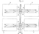
図2は、とくに、インバータの直流回路に対するモジュール2、3、4、7の接続部を示している。モジュール2、3、4が直流電流から、各位相に対応する交流電流を生成する半導体モジュールであるということは、図1を参照しつつすでに説明したことである。用いられているスイッチング素子は、例えば、サイリスタ、IGBT又はその他の半導体である。この構造は、これらのモジュール2、3、4、7に直流電流を供給するために、モジュール2、3、4、7に接続された接続プレート12、13、16、17を有している。この接続部は、一方ではネジ21によってモジュール2、3、4、7に取り付けられ、他方では接続プレート12、13、16、17に取り付けられた棒状部材10、11、14、15(bar)によって形成されている。棒状部材10、11、14、15は、接続プレート12、13、16、17と同様に、電位(potential)に従って分離されている。この実施の形態においては、例えば、プレート12、16を陽極として正の電位を印加することができる。また、プレート13、17を陰極として負の電位又はアース電位を印加することができる。その結果、この場合は、棒状部材10、14は正の電位となり、棒状部材11、15は負の電位又はアース電位となるということが理解されるであろう。
FIG. 2 shows in particular the connections of the
モジュール2、3、4、7に電力を供給するために棒状部材10、11、14、15を用いることは、それ相応に棒状部材の断面を大きくすることができ、それ相応に大電流を流すことができるということを意味する。取り扱い性を改善するため、棒状部材10、11、14、15を分割し、各個別の棒状部材10、11、14、15が接続プレートからモジュール2、3、4、7に伸びるようにしてもよい。
The use of
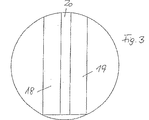
図2からわかるように、接続プレート12、13、16、17の後側に、さらなるプレート18、19が、互いに平行な位置関係でもって配置されている。これらのプレート18、19の構造及び動作モードは、図3を参照しつつより詳しく説明されるであろう。なお、図3は、図2中において円で囲まれた部分を拡大して示した図である。
As can be seen from FIG. 2,
図3は、3層構造を示している。この3層構造は、2つのコンデンサプレート18、19と誘電体20とで形成されている。したがって、この構造は、プレートコンデンサを形成する。この場合、コンデンサのプレート18、19は、例えば、アルミニウムで製作することができ、数ミリメートルの厚さのものであってもよい。誘電体20は、プラスチックのフィルム又はシートで形成することができ、1ミリメートルの1/10の数倍(some tenths of a millimetre)の厚さのものであってもよい。この構造においては、プレート18、19の一方は必然的に陽極であり、他方のプレートは必然的に陰極プレートである。コンデンサのプレート18、19は、モジュール2、3、4、7に直流電流を供給するために用いられる。この供給手段がプレートコンデンサの形態であるといった事実から、この供給は純粋に容量性であり、望ましくないインダクタンスの影響が回避されるということがわかる。コンデンサプレート18が陰極プレートである場合、接続プレート13、17はコンデンサプレート18に接続される。これと対応する仕様で、接続プレート12、16は、陽極プレートとして機能するコンデンサプレート19に接続される。
FIG. 3 shows a three-layer structure. This three-layer structure is formed by two
図4は、とくに半導体スイッチング素子22を備えた半導体モジュール2、3、4の単純化された図である。例えばIGBTが用いられるこれらの半導体スイッチング素子22は、ケーブル25によって取り出される所望の交流電流を生成するために、当該技術分野で知られている適切な手法で駆動される。かかる半導体モジュールの動作モードは、例えば、ドイツ特許第197 48 479 C1号明細書に開示されている。
FIG. 4 is a simplified diagram of the
ケーブル端子用突起24(cable terminal lug)を備えたケーブル25間の間隔を限定し、これにより当然にケーブル25間の間隔を予め設定された大きさにするために、半導体スイッチング素子22に、適切に構成された接続端子を設けてもよい。また、半導体モジュール22の出力端子からケーブル接続用突起24まで棒状部材23が設けられ、これらの棒状部材23は、半導体素子22の出力電流を対応するケーブル25に流す。これらの棒状部材23は、ネジ26により、半導体モジュール22の出力端子に固定されている。ここで、これらのネジは、頭部に六角形の凹部を備えた形態のものである。ケーブル25は、順に、十字形頭部ネジの形態のものであるネジ26とケーブル接続用突起24とにより、棒状部材23に固定されている。この構造は、ケーブル25内の電流の流れを監視するために、2つのケーブル25を、ともに、変流器(current transformer)のフェライトリング(ferrite ring)などの測定値取り出し装置を通り抜けさせることを可能にする。
In order to limit the distance between the
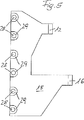
本発明によれば、インバータは、複数のコンデンサで形成された中間蓄電手段を有している。この中間蓄電手段を設ける目的は、とくには、半導体モジュールに印加される直流電圧を平滑化し(smooth)、半導体スイッチング素子22のスイッチング動作の結果として生じる電圧変動を補償することである。この目的を達するため、中間蓄電手段(図示せず)は、プレートコンデンサ18、19、20によりモジュールに接続されている。図5及び図6に、プレートコンデンサのプレート18、19が示されている。ここで、図5は陽極プレートを示し、図6は陰極プレートを示している。これらのプレート18、19は、穴部28と、これらの穴部のまわりで広がっている凹部29とを有している。図7中には、一例として、穴部/凹部の断面が詳細に示されている。
According to the present invention, the inverter has intermediate power storage means formed of a plurality of capacitors. The purpose of providing this intermediate power storage means is, in particular, to smooth the DC voltage applied to the semiconductor module and to compensate for voltage fluctuations that occur as a result of the switching operation of the
この構造により、一方では中間蓄電手段を形成しているコンデンサ(図示せず)をネジ留め手段によりプレート18、19に接続することが可能となり、これにより、もし必要があれば、個々のコンデンサを交換することができる。そして、ネジの頭部が凹部29内に沈み込んでいるこの構造により、誘電体(図3中の参照番号20)の間隔のみにより、プレートを、互いに分離された互いに平行な位置関係で配置することができる。図5及び図6に示されたプレートを比較すれば、接続用の棒状部材のための接続プレート12、13、16、17が、高さに関して互いにずれた位置関係(displaced relationship)にあり、これにより図2中に示されたねじれ形の配置(staggered arrangement)とすることができることがわかる。
This structure, on the one hand, allows capacitors (not shown) forming intermediate storage means to be connected to the
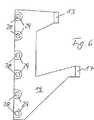
図8は、図2に示された接続用の棒状部材10、11、14、15の代替的な構成を示している。ここで、棒状部材は、両接続プレート12、13を覆うように広げられている。この図においてプレートの形態であるこれらの棒状部材は、参照番号31、32で示されている。両者が互いに重なり合った位置関係で配置されていることを明確にするため、これらは互いに移動させられて図示されている。本来の位置関係では、これらは実質的に、一方が他方の上に重なり合った位置関係で配置される。
FIG. 8 shows an alternative configuration of the connecting
この場合、一方のプレートは陽極12に接続され、他方は陰極13に接続される。この図には示されていないが、これらのプレート31、32はまた、プレート31、32間に挿入された誘電体により、コンデンサを形成している。この図においては、プレート32は陽極プレートであり、プレート31は陰極プレートである。こここでもまた、これらのプレートは、それらに必要な直流電流を供給するために、この図には示されていない半導体モジュールに適切に接続されていることがわかるであろう。接続プレート12、13はまた、プレートコンデンサにより半導体モジュールにも接続されているので、インダクタンスの影響(inductive influence)は、電気的接続のこの部分で防止される。
In this case, one plate is connected to the
それゆえ、これは、中間蓄電手段から半導体モジュールの入力端子への容量性接続部を含んでいる。 This therefore includes a capacitive connection from the intermediate power storage means to the input terminal of the semiconductor module.
1 キャビネット、2 モジュール、3 モジュール、4 モジュール、5 モジュール、6 モジュール、7 モジュール、10 棒状部材、11 棒状部材、12 プレート、13 プレート、14 棒状部材、15 棒状部材、16 プレート、17 プレート、18 プレート、19 プレート、20 誘電体、21 ネジ、22 半導体スイッチング素子、23 棒状部材、24 ケーブル端子用突起、25 ケーブル。
1 cabinet, 2 modules, 3 modules, 4 modules, 5 modules, 6 modules, 7 modules, 10 rod members, 11 rod members, 12 plates, 13 plates, 14 rod members, 15 rod members, 16 plates, 17 plates, 18 Plate, 19 Plate, 20 Dielectric, 21 Screw, 22 Semiconductor switching element, 23 Bar-shaped member, 24 Projection for cable terminal, 25 Cable.
Claims (3)
上記モジュールのうち、半導体モジュール(2、3、4)である少なくとも一部のモジュール(2、3、4)に取り外し可能に取り付けられた接続線であって、各半導体モジュール(2、3、4)はそれぞれインバータの各位相に対して、直流電流から交流電流を生成するように構成されているものと、
複数のコンデンサで形成された中間蓄電手段と、
上記中間蓄電手段と上記半導体モジュール(2、3、4)との間の容量性接続部とを備えているインバータであって、
上記容量性接続部は少なくとも1つのプレートコンデンサ(18、19、20、31、32)を含み、
上記プレートコンデンサ(18、19、31、32)のプレートが、上記半導体モジュール(2、3、4)に機械的にかつ電気的に接続される一方、上記中間蓄電手段の上記コンデンサに機械的かつ電気的に取り外し可能に接続されているインバータ。 A module structure that is at least partially modular having removably mounted modules (2,3,4,5,6,7),
Among the above modules, a connection line detachably attached to at least a part of the modules (2, 3, 4) which are the semiconductor modules (2, 3, 4), and each of the semiconductor modules (2, 3, 4). ) Is configured to generate an alternating current from a direct current for each phase of the inverter,
Intermediate power storage means formed of a plurality of capacitors;
An inverter comprising a capacitive connection between the intermediate power storage means and the semiconductor module (2, 3, 4),
The capacitive connection includes at least one plate capacitor (18, 19, 20, 31, 32);
While the upper plate's rating plate capacitor (18,19,31,32) is, Ru is mechanically and electrically connected to the semiconductor module (2, 3, 4), mechanically the capacitor of the intermediate storage means And an inverter that is electrically removably connected .
Applications Claiming Priority (2)
| Application Number | Priority Date | Filing Date | Title |
|---|---|---|---|
| DE10161178A DE10161178A1 (en) | 2001-12-13 | 2001-12-13 | inverter |
| PCT/EP2002/014031 WO2003050938A2 (en) | 2001-12-13 | 2002-12-11 | Power inverter |
Publications (2)
| Publication Number | Publication Date |
|---|---|
| JP2005517372A JP2005517372A (en) | 2005-06-09 |
| JP4153875B2 true JP4153875B2 (en) | 2008-09-24 |
Family
ID=7709023
Family Applications (1)
| Application Number | Title | Priority Date | Filing Date |
|---|---|---|---|
| JP2003551887A Expired - Lifetime JP4153875B2 (en) | 2001-12-13 | 2002-12-11 | Inverter |
Country Status (22)
| Country | Link |
|---|---|
| US (1) | US7492621B2 (en) |
| EP (1) | EP1466398B1 (en) |
| JP (1) | JP4153875B2 (en) |
| KR (1) | KR20040068218A (en) |
| CN (1) | CN1602578A (en) |
| AR (1) | AR037820A1 (en) |
| AT (1) | ATE346418T1 (en) |
| AU (1) | AU2002361386B2 (en) |
| BR (1) | BR0214797A (en) |
| CA (1) | CA2470129C (en) |
| CY (1) | CY1107581T1 (en) |
| DE (2) | DE10161178A1 (en) |
| DK (1) | DK1466398T3 (en) |
| ES (1) | ES2275020T3 (en) |
| MA (1) | MA26254A1 (en) |
| MX (1) | MXPA04005547A (en) |
| NO (1) | NO324910B1 (en) |
| NZ (1) | NZ533522A (en) |
| PL (1) | PL219079B1 (en) |
| PT (1) | PT1466398E (en) |
| WO (1) | WO2003050938A2 (en) |
| ZA (1) | ZA200404506B (en) |
Families Citing this family (70)
| Publication number | Priority date | Publication date | Assignee | Title |
|---|---|---|---|---|
| DE10161178A1 (en) | 2001-12-13 | 2003-07-10 | Aloys Wobben | inverter |
| US11881814B2 (en) | 2005-12-05 | 2024-01-23 | Solaredge Technologies Ltd. | Testing of a photovoltaic panel |
| US8324921B2 (en) | 2007-12-05 | 2012-12-04 | Solaredge Technologies Ltd. | Testing of a photovoltaic panel |
| US10693415B2 (en) | 2007-12-05 | 2020-06-23 | Solaredge Technologies Ltd. | Testing of a photovoltaic panel |
| FI120899B (en) * | 2005-12-21 | 2010-04-15 | Vacon Oyj | Arrangement and procedure for placing a drive in a cabinet |
| AT504199A1 (en) | 2006-09-04 | 2008-03-15 | Fronius Int Gmbh | MODULAR INVERTER SYSTEM |
| US9112379B2 (en) | 2006-12-06 | 2015-08-18 | Solaredge Technologies Ltd. | Pairing of components in a direct current distributed power generation system |
| US8618692B2 (en) | 2007-12-04 | 2013-12-31 | Solaredge Technologies Ltd. | Distributed power system using direct current power sources |
| US8963369B2 (en) | 2007-12-04 | 2015-02-24 | Solaredge Technologies Ltd. | Distributed power harvesting systems using DC power sources |
| US8947194B2 (en) | 2009-05-26 | 2015-02-03 | Solaredge Technologies Ltd. | Theft detection and prevention in a power generation system |
| US11569659B2 (en) | 2006-12-06 | 2023-01-31 | Solaredge Technologies Ltd. | Distributed power harvesting systems using DC power sources |
| US11296650B2 (en) | 2006-12-06 | 2022-04-05 | Solaredge Technologies Ltd. | System and method for protection during inverter shutdown in distributed power installations |
| US11735910B2 (en) | 2006-12-06 | 2023-08-22 | Solaredge Technologies Ltd. | Distributed power system using direct current power sources |
| US11728768B2 (en) | 2006-12-06 | 2023-08-15 | Solaredge Technologies Ltd. | Pairing of components in a direct current distributed power generation system |
| US8473250B2 (en) | 2006-12-06 | 2013-06-25 | Solaredge, Ltd. | Monitoring of distributed power harvesting systems using DC power sources |
| US8013472B2 (en) | 2006-12-06 | 2011-09-06 | Solaredge, Ltd. | Method for distributed power harvesting using DC power sources |
| US11309832B2 (en) | 2006-12-06 | 2022-04-19 | Solaredge Technologies Ltd. | Distributed power harvesting systems using DC power sources |
| US8816535B2 (en) | 2007-10-10 | 2014-08-26 | Solaredge Technologies, Ltd. | System and method for protection during inverter shutdown in distributed power installations |
| US9130401B2 (en) | 2006-12-06 | 2015-09-08 | Solaredge Technologies Ltd. | Distributed power harvesting systems using DC power sources |
| US11687112B2 (en) | 2006-12-06 | 2023-06-27 | Solaredge Technologies Ltd. | Distributed power harvesting systems using DC power sources |
| US9088178B2 (en) | 2006-12-06 | 2015-07-21 | Solaredge Technologies Ltd | Distributed power harvesting systems using DC power sources |
| US8384243B2 (en) | 2007-12-04 | 2013-02-26 | Solaredge Technologies Ltd. | Distributed power harvesting systems using DC power sources |
| US11888387B2 (en) | 2006-12-06 | 2024-01-30 | Solaredge Technologies Ltd. | Safety mechanisms, wake up and shutdown methods in distributed power installations |
| WO2008125915A2 (en) * | 2006-12-06 | 2008-10-23 | Solaredge, Ltd. | Monitoring of distributed power harvesting systems using dc power sources |
| US8319471B2 (en) | 2006-12-06 | 2012-11-27 | Solaredge, Ltd. | Battery power delivery module |
| US8319483B2 (en) | 2007-08-06 | 2012-11-27 | Solaredge Technologies Ltd. | Digital average input current control in power converter |
| US11855231B2 (en) | 2006-12-06 | 2023-12-26 | Solaredge Technologies Ltd. | Distributed power harvesting systems using DC power sources |
| US7900361B2 (en) | 2006-12-06 | 2011-03-08 | Solaredge, Ltd. | Current bypass for distributed power harvesting systems using DC power sources |
| DE102008034417B4 (en) | 2007-09-25 | 2023-03-16 | Sew-Eurodrive Gmbh & Co Kg | converter |
| US11264947B2 (en) | 2007-12-05 | 2022-03-01 | Solaredge Technologies Ltd. | Testing of a photovoltaic panel |
| EP2232690B1 (en) | 2007-12-05 | 2016-08-31 | Solaredge Technologies Ltd. | Parallel connected inverters |
| WO2009072075A2 (en) | 2007-12-05 | 2009-06-11 | Solaredge Technologies Ltd. | Photovoltaic system power tracking method |
| US8049523B2 (en) | 2007-12-05 | 2011-11-01 | Solaredge Technologies Ltd. | Current sensing on a MOSFET |
| JP2011507465A (en) | 2007-12-05 | 2011-03-03 | ソラレッジ テクノロジーズ リミテッド | Safety mechanism, wake-up method and shutdown method in distributed power installation |
| EP2269290B1 (en) | 2008-03-24 | 2018-12-19 | Solaredge Technologies Ltd. | Switch mode converter including active clamp for achieving zero voltage switching |
| EP2294669B8 (en) | 2008-05-05 | 2016-12-07 | Solaredge Technologies Ltd. | Direct current power combiner |
| US8461453B2 (en) * | 2009-01-27 | 2013-06-11 | Connector Manufacturing Company | Wind turbine wiring enclosure cabinet |
| EP2427915B1 (en) | 2009-05-22 | 2013-09-11 | Solaredge Technologies Ltd. | Electrically isolated heat dissipating junction box |
| US8303349B2 (en) | 2009-05-22 | 2012-11-06 | Solaredge Technologies Ltd. | Dual compressive connector |
| US8690110B2 (en) | 2009-05-25 | 2014-04-08 | Solaredge Technologies Ltd. | Bracket for connection of a junction box to photovoltaic panels |
| DE102009051518B3 (en) * | 2009-10-31 | 2011-05-12 | Semikron Elektronik Gmbh & Co. Kg | Modular converter arrangement |
| US8710699B2 (en) | 2009-12-01 | 2014-04-29 | Solaredge Technologies Ltd. | Dual use photovoltaic system |
| US8766696B2 (en) | 2010-01-27 | 2014-07-01 | Solaredge Technologies Ltd. | Fast voltage level shifter circuit |
| GB2485527B (en) | 2010-11-09 | 2012-12-19 | Solaredge Technologies Ltd | Arc detection and prevention in a power generation system |
| US10230310B2 (en) | 2016-04-05 | 2019-03-12 | Solaredge Technologies Ltd | Safety switch for photovoltaic systems |
| US10673222B2 (en) | 2010-11-09 | 2020-06-02 | Solaredge Technologies Ltd. | Arc detection and prevention in a power generation system |
| US10673229B2 (en) | 2010-11-09 | 2020-06-02 | Solaredge Technologies Ltd. | Arc detection and prevention in a power generation system |
| US9118213B2 (en) | 2010-11-24 | 2015-08-25 | Kohler Co. | Portal for harvesting energy from distributed electrical power sources |
| GB2486408A (en) | 2010-12-09 | 2012-06-20 | Solaredge Technologies Ltd | Disconnection of a string carrying direct current |
| GB2483317B (en) | 2011-01-12 | 2012-08-22 | Solaredge Technologies Ltd | Serially connected inverters |
| US8570005B2 (en) | 2011-09-12 | 2013-10-29 | Solaredge Technologies Ltd. | Direct current link circuit |
| GB2498365A (en) | 2012-01-11 | 2013-07-17 | Solaredge Technologies Ltd | Photovoltaic module |
| GB2498790A (en) | 2012-01-30 | 2013-07-31 | Solaredge Technologies Ltd | Maximising power in a photovoltaic distributed power system |
| GB2498791A (en) | 2012-01-30 | 2013-07-31 | Solaredge Technologies Ltd | Photovoltaic panel circuitry |
| US9853565B2 (en) | 2012-01-30 | 2017-12-26 | Solaredge Technologies Ltd. | Maximized power in a photovoltaic distributed power system |
| GB2499991A (en) | 2012-03-05 | 2013-09-11 | Solaredge Technologies Ltd | DC link circuit for photovoltaic array |
| WO2013177360A1 (en) | 2012-05-25 | 2013-11-28 | Solaredge Technologies Ltd. | Circuit for interconnected direct current power sources |
| US10115841B2 (en) | 2012-06-04 | 2018-10-30 | Solaredge Technologies Ltd. | Integrated photovoltaic panel circuitry |
| US9941813B2 (en) | 2013-03-14 | 2018-04-10 | Solaredge Technologies Ltd. | High frequency multi-level inverter |
| US9548619B2 (en) | 2013-03-14 | 2017-01-17 | Solaredge Technologies Ltd. | Method and apparatus for storing and depleting energy |
| EP3506370B1 (en) | 2013-03-15 | 2023-12-20 | Solaredge Technologies Ltd. | Bypass mechanism |
| EP2814308B1 (en) * | 2013-06-10 | 2019-06-26 | SEMIKRON Elektronik GmbH & Co. KG | 3 level power converter |
| US9318974B2 (en) | 2014-03-26 | 2016-04-19 | Solaredge Technologies Ltd. | Multi-level inverter with flying capacitor topology |
| US10599113B2 (en) | 2016-03-03 | 2020-03-24 | Solaredge Technologies Ltd. | Apparatus and method for determining an order of power devices in power generation systems |
| US11081608B2 (en) | 2016-03-03 | 2021-08-03 | Solaredge Technologies Ltd. | Apparatus and method for determining an order of power devices in power generation systems |
| CN107153212B (en) | 2016-03-03 | 2023-07-28 | 太阳能安吉科技有限公司 | Method for mapping a power generation facility |
| US11018623B2 (en) | 2016-04-05 | 2021-05-25 | Solaredge Technologies Ltd. | Safety switch for photovoltaic systems |
| US11177663B2 (en) | 2016-04-05 | 2021-11-16 | Solaredge Technologies Ltd. | Chain of power devices |
| JP2020144492A (en) * | 2019-03-05 | 2020-09-10 | 株式会社チノー | Heating element cooling structure |
| KR102314048B1 (en) * | 2019-10-15 | 2021-10-19 | 한국전력공사 | Apparatus and Method for converting power intelligently |
Family Cites Families (39)
| Publication number | Priority date | Publication date | Assignee | Title |
|---|---|---|---|---|
| FR2586139B1 (en) | 1985-08-12 | 1987-10-30 | Commissariat Energie Atomique | MAGNETIC MIRROR ION DIODE |
| DE3609065A1 (en) | 1986-03-18 | 1987-09-24 | Siemens Ag | LOW-INDUCTIVE RAILING |
| US4684191A (en) | 1986-06-30 | 1987-08-04 | Amp Incorporated | Electrical terminal and electrical connector assembly |
| US4845589A (en) | 1987-05-04 | 1989-07-04 | Amp Incorporated | Bus bar connector assembly |
| DE3802593A1 (en) | 1988-01-29 | 1989-08-10 | Heidelberger Druckmasch Ag | CONVERTER WITH DC INTERMEDIATE CIRCUIT |
| US4867696A (en) | 1988-07-15 | 1989-09-19 | Amp Incorporated | Laminated bus bar with power tabs |
| US4908258A (en) | 1988-08-01 | 1990-03-13 | Rogers Corporation | High dielectric constant flexible sheet material |
| GB2242580B (en) | 1990-03-30 | 1994-06-15 | Mitsubishi Electric Corp | Inverter unit with improved bus-plate configuration |
| US5579217A (en) | 1991-07-10 | 1996-11-26 | Kenetech Windpower, Inc. | Laminated bus assembly and coupling apparatus for a high power electrical switching converter |
| US5365424A (en) | 1991-07-10 | 1994-11-15 | Kenetech Windpower, Inc. | High power laminated bus assembly for an electrical switching converter |
| US5172310A (en) * | 1991-07-10 | 1992-12-15 | U.S. Windpower, Inc. | Low impedance bus for power electronics |
| US5164624A (en) | 1991-09-06 | 1992-11-17 | General Motors Corporation | Modular power semiconductor assembly for an alternator-fed DC power source |
| US5253613A (en) | 1992-04-30 | 1993-10-19 | General Electric Company | High power AC traction inverter cooling |
| DE4232763C2 (en) | 1992-09-25 | 1995-12-14 | Aeg Westinghouse Transport | Construction of an inverter, in particular a 3-point inverter |
| JP2809026B2 (en) * | 1992-09-30 | 1998-10-08 | 三菱電機株式会社 | INVERTER DEVICE AND METHOD OF USING INVERTER DEVICE |
| US5434770A (en) | 1992-11-20 | 1995-07-18 | United States Department Of Energy | High voltage power supply with modular series resonant inverters |
| DE4301342C1 (en) | 1993-01-20 | 1994-04-14 | Niesing Stahlbau Stahlschornst | Wind- or water-powered electricity generator - has drive coupling having adjustable transmission ratio adjusted to maintain constant generator revolutions. |
| DE9303886U1 (en) | 1993-03-16 | 1993-06-17 | Siemens Nixdorf Informationssysteme Ag, 4790 Paderborn, De | |
| US5422440A (en) | 1993-06-08 | 1995-06-06 | Rem Technologies, Inc. | Low inductance bus bar arrangement for high power inverters |
| DE4412990A1 (en) | 1994-04-15 | 1995-10-19 | Abb Patent Gmbh | Power converter system with liquid or air-cooled power semiconductors and DC link |
| US5517063A (en) | 1994-06-10 | 1996-05-14 | Westinghouse Electric Corp. | Three phase power bridge assembly |
| DE19519538A1 (en) | 1995-05-27 | 1996-11-28 | Export Contor Ausenhandelsgese | Power semiconductor circuit with multiple paired power semiconductor devices |
| DE19711016A1 (en) | 1996-05-21 | 1997-11-27 | Siemens Ag | Inverters with a modular design |
| US5808240A (en) | 1996-05-24 | 1998-09-15 | Otis Elevator Company | Low-inductance planar bus arrangement |
| EP0914708B1 (en) | 1996-07-22 | 2002-09-04 | Hydro-Quebec | Low stray interconnection inductance power converting module for converting a dc voltage into an ac voltage, and a method therefor |
| DE19732402B4 (en) | 1997-07-28 | 2004-07-15 | Danfoss Drives A/S | Electrical bus arrangement for the direct current supply of circuit elements of an inverter |
| JPH1169840A (en) | 1997-08-22 | 1999-03-09 | Aisin Seiki Co Ltd | Switching assembly |
| DE19748479C1 (en) | 1997-11-03 | 1999-04-15 | Aloys Wobben | AC current converter with variable pulse frequency |
| JP3424532B2 (en) | 1997-11-25 | 2003-07-07 | 株式会社日立製作所 | Power converter |
| JPH11262135A (en) | 1998-03-13 | 1999-09-24 | Sumitomo Wiring Syst Ltd | Assembling structure of laminated bus bar |
| FR2777109B1 (en) | 1998-04-06 | 2000-08-04 | Gec Alsthom Transport Sa | CAPACITOR BATTERY, ELECTRONIC POWER DEVICE COMPRISING SUCH A BATTERY AND ELECTRONIC POWER ASSEMBLY COMPRISING SUCH A DEVICE |
| US6160696A (en) | 1998-05-04 | 2000-12-12 | General Electric Company | Modular bus bar and switch assembly for traction inverter |
| JPH11346480A (en) * | 1998-06-02 | 1999-12-14 | Hitachi Ltd | Inverter device |
| DE19847029A1 (en) | 1998-10-13 | 2000-04-27 | Semikron Elektronik Gmbh | Converter with low-inductance capacitor in the intermediate circuit |
| US6212087B1 (en) | 1999-02-05 | 2001-04-03 | International Rectifier Corp. | Electronic half bridge module |
| JP3624798B2 (en) * | 2000-06-07 | 2005-03-02 | 株式会社村田製作所 | Inverter capacitor module, inverter |
| DE10161178A1 (en) | 2001-12-13 | 2003-07-10 | Aloys Wobben | inverter |
| US7046535B2 (en) * | 2003-12-17 | 2006-05-16 | Ballard Power Systems Corporation | Architecture for power modules such as power inverters |
| US7289343B2 (en) * | 2003-12-17 | 2007-10-30 | Siemens Vdo Automotive Corporation | Architecture for power modules such as power inverters |
-
2001
- 2001-12-13 DE DE10161178A patent/DE10161178A1/en not_active Withdrawn
-
2002
- 2002-12-11 PL PL368990A patent/PL219079B1/en unknown
- 2002-12-11 BR BR0214797-1A patent/BR0214797A/en not_active Application Discontinuation
- 2002-12-11 JP JP2003551887A patent/JP4153875B2/en not_active Expired - Lifetime
- 2002-12-11 EP EP02796603A patent/EP1466398B1/en not_active Revoked
- 2002-12-11 CA CA002470129A patent/CA2470129C/en not_active Expired - Lifetime
- 2002-12-11 NZ NZ533522A patent/NZ533522A/en not_active IP Right Cessation
- 2002-12-11 PT PT02796603T patent/PT1466398E/en unknown
- 2002-12-11 CN CNA028246977A patent/CN1602578A/en active Pending
- 2002-12-11 DE DE50208811T patent/DE50208811D1/en not_active Expired - Lifetime
- 2002-12-11 WO PCT/EP2002/014031 patent/WO2003050938A2/en active IP Right Grant
- 2002-12-11 US US10/497,953 patent/US7492621B2/en active Active
- 2002-12-11 KR KR10-2004-7008993A patent/KR20040068218A/en not_active Application Discontinuation
- 2002-12-11 ES ES02796603T patent/ES2275020T3/en not_active Expired - Lifetime
- 2002-12-11 DK DK02796603T patent/DK1466398T3/en active
- 2002-12-11 MX MXPA04005547A patent/MXPA04005547A/en active IP Right Grant
- 2002-12-11 AT AT02796603T patent/ATE346418T1/en active
- 2002-12-11 AU AU2002361386A patent/AU2002361386B2/en not_active Ceased
- 2002-12-13 AR ARP020104837A patent/AR037820A1/en not_active Application Discontinuation
-
2004
- 2004-06-07 MA MA27722A patent/MA26254A1/en unknown
- 2004-06-08 ZA ZA2004/04506A patent/ZA200404506B/en unknown
- 2004-07-12 NO NO20042933A patent/NO324910B1/en not_active IP Right Cessation
-
2007
- 2007-01-18 CY CY20071100076T patent/CY1107581T1/en unknown
Also Published As
| Publication number | Publication date |
|---|---|
| WO2003050938A2 (en) | 2003-06-19 |
| NO324910B1 (en) | 2008-01-07 |
| KR20040068218A (en) | 2004-07-30 |
| PL219079B1 (en) | 2015-03-31 |
| AU2002361386A1 (en) | 2003-06-23 |
| AU2002361386B2 (en) | 2005-06-30 |
| US20050122692A1 (en) | 2005-06-09 |
| NZ533522A (en) | 2005-12-23 |
| DK1466398T3 (en) | 2007-03-26 |
| WO2003050938A3 (en) | 2003-11-20 |
| ES2275020T3 (en) | 2007-06-01 |
| CA2470129A1 (en) | 2003-06-19 |
| CN1602578A (en) | 2005-03-30 |
| JP2005517372A (en) | 2005-06-09 |
| PL368990A1 (en) | 2005-04-04 |
| EP1466398B1 (en) | 2006-11-22 |
| DE10161178A1 (en) | 2003-07-10 |
| US7492621B2 (en) | 2009-02-17 |
| MXPA04005547A (en) | 2004-09-10 |
| MA26254A1 (en) | 2004-08-01 |
| BR0214797A (en) | 2004-10-19 |
| PT1466398E (en) | 2007-01-31 |
| AR037820A1 (en) | 2004-12-09 |
| NO20042933L (en) | 2004-07-12 |
| ZA200404506B (en) | 2005-01-26 |
| EP1466398A2 (en) | 2004-10-13 |
| CA2470129C (en) | 2007-08-07 |
| DE50208811D1 (en) | 2007-01-04 |
| CY1107581T1 (en) | 2013-03-13 |
| ATE346418T1 (en) | 2006-12-15 |
Similar Documents
| Publication | Publication Date | Title |
|---|---|---|
| JP4153875B2 (en) | Inverter | |
| EP2092631B1 (en) | Removable component cartridge for increasing reliability in power harvesting systems | |
| JP5504118B2 (en) | Modular converter device | |
| JP5300988B2 (en) | Series circuit of on-off controllers for transferring energy in battery systems | |
| US7965526B2 (en) | Self powered supply for power converter switch driver | |
| US8879292B2 (en) | Multipoint converters with brake chopper | |
| RU2516296C2 (en) | System of batteries, power supply system for electric rail vehicles and battery module | |
| KR20090132507A (en) | Solar power plant | |
| RU2702218C1 (en) | Power cell with printed circuit boards and decoupler and multicell power supply medium voltage source | |
| US9787173B2 (en) | Multilevel converter | |
| JPH10164843A (en) | Power conversion apparatus | |
| US20150249402A1 (en) | Dc power transmission systems and method of assembling the same | |
| JP5003618B2 (en) | Fuel cell power converter | |
| CN105490558A (en) | Diode clamped three-level converter and power system thereof | |
| CN219107307U (en) | Switching power supply device and converter | |
| CN212726881U (en) | Brake assembly of three-level converter and three-level converter | |
| JP5134839B2 (en) | Gate pulse generation circuit for power converter | |
| NL2019057B1 (en) | AC to DC converter | |
| JP7399804B2 (en) | Current interrupter | |
| EP3972101A1 (en) | Modular conversion system with individual bridge outputs and stacked dc-link balancing by means of zero-vector switching | |
| KR20210058364A (en) | Modular inverter system by function | |
| JP5957303B2 (en) | Power conversion device and distributed power supply system | |
| Fang et al. | Four quadrant 250 kW switchmode power supply for Fermilab Main Injector | |
| KR20060054734A (en) | Advanced power conveter using pwm-inverter |
Legal Events
| Date | Code | Title | Description |
|---|---|---|---|
| A131 | Notification of reasons for refusal |
Free format text: JAPANESE INTERMEDIATE CODE: A131 Effective date: 20061031 |
|
| A601 | Written request for extension of time |
Free format text: JAPANESE INTERMEDIATE CODE: A601 Effective date: 20070131 |
|
| RD03 | Notification of appointment of power of attorney |
Free format text: JAPANESE INTERMEDIATE CODE: A7423 Effective date: 20070131 |
|
| A602 | Written permission of extension of time |
Free format text: JAPANESE INTERMEDIATE CODE: A602 Effective date: 20070207 |
|
| A521 | Request for written amendment filed |
Free format text: JAPANESE INTERMEDIATE CODE: A523 Effective date: 20070501 |
|
| A131 | Notification of reasons for refusal |
Free format text: JAPANESE INTERMEDIATE CODE: A131 Effective date: 20071023 |
|
| A521 | Request for written amendment filed |
Free format text: JAPANESE INTERMEDIATE CODE: A523 Effective date: 20080115 |
|
| TRDD | Decision of grant or rejection written | ||
| A01 | Written decision to grant a patent or to grant a registration (utility model) |
Free format text: JAPANESE INTERMEDIATE CODE: A01 Effective date: 20080610 |
|
| A01 | Written decision to grant a patent or to grant a registration (utility model) |
Free format text: JAPANESE INTERMEDIATE CODE: A01 |
|
| A61 | First payment of annual fees (during grant procedure) |
Free format text: JAPANESE INTERMEDIATE CODE: A61 Effective date: 20080704 |
|
| R150 | Certificate of patent or registration of utility model |
Free format text: JAPANESE INTERMEDIATE CODE: R150 Ref document number: 4153875 Country of ref document: JP Free format text: JAPANESE INTERMEDIATE CODE: R150 |
|
| FPAY | Renewal fee payment (event date is renewal date of database) |
Free format text: PAYMENT UNTIL: 20110711 Year of fee payment: 3 |
|
| FPAY | Renewal fee payment (event date is renewal date of database) |
Free format text: PAYMENT UNTIL: 20120711 Year of fee payment: 4 |
|
| R250 | Receipt of annual fees |
Free format text: JAPANESE INTERMEDIATE CODE: R250 |
|
| FPAY | Renewal fee payment (event date is renewal date of database) |
Free format text: PAYMENT UNTIL: 20130711 Year of fee payment: 5 |
|
| R250 | Receipt of annual fees |
Free format text: JAPANESE INTERMEDIATE CODE: R250 |
|
| R250 | Receipt of annual fees |
Free format text: JAPANESE INTERMEDIATE CODE: R250 |
|
| R250 | Receipt of annual fees |
Free format text: JAPANESE INTERMEDIATE CODE: R250 |
|
| R250 | Receipt of annual fees |
Free format text: JAPANESE INTERMEDIATE CODE: R250 |
|
| R250 | Receipt of annual fees |
Free format text: JAPANESE INTERMEDIATE CODE: R250 |
|
| R250 | Receipt of annual fees |
Free format text: JAPANESE INTERMEDIATE CODE: R250 |
|
| R250 | Receipt of annual fees |
Free format text: JAPANESE INTERMEDIATE CODE: R250 |
|
| R250 | Receipt of annual fees |
Free format text: JAPANESE INTERMEDIATE CODE: R250 |
|
| R250 | Receipt of annual fees |
Free format text: JAPANESE INTERMEDIATE CODE: R250 |
|
| R250 | Receipt of annual fees |
Free format text: JAPANESE INTERMEDIATE CODE: R250 |
|
| R250 | Receipt of annual fees |
Free format text: JAPANESE INTERMEDIATE CODE: R250 |
|
| EXPY | Cancellation because of completion of term |