EP3972101A1 - Modular conversion system with individual bridge outputs and stacked dc-link balancing by means of zero-vector switching - Google Patents
Modular conversion system with individual bridge outputs and stacked dc-link balancing by means of zero-vector switching Download PDFInfo
- Publication number
- EP3972101A1 EP3972101A1 EP21194742.9A EP21194742A EP3972101A1 EP 3972101 A1 EP3972101 A1 EP 3972101A1 EP 21194742 A EP21194742 A EP 21194742A EP 3972101 A1 EP3972101 A1 EP 3972101A1
- Authority
- EP
- European Patent Office
- Prior art keywords
- switch
- voltage
- side capacitor
- electrically connected
- switches
- Prior art date
- Legal status (The legal status is an assumption and is not a legal conclusion. Google has not performed a legal analysis and makes no representation as to the accuracy of the status listed.)
- Pending
Links
Images


Classifications
-
- H—ELECTRICITY
- H02—GENERATION; CONVERSION OR DISTRIBUTION OF ELECTRIC POWER
- H02M—APPARATUS FOR CONVERSION BETWEEN AC AND AC, BETWEEN AC AND DC, OR BETWEEN DC AND DC, AND FOR USE WITH MAINS OR SIMILAR POWER SUPPLY SYSTEMS; CONVERSION OF DC OR AC INPUT POWER INTO SURGE OUTPUT POWER; CONTROL OR REGULATION THEREOF
- H02M1/00—Details of apparatus for conversion
- H02M1/0067—Converter structures employing plural converter units, other than for parallel operation of the units on a single load
- H02M1/0074—Plural converter units whose inputs are connected in series
-
- H—ELECTRICITY
- H02—GENERATION; CONVERSION OR DISTRIBUTION OF ELECTRIC POWER
- H02M—APPARATUS FOR CONVERSION BETWEEN AC AND AC, BETWEEN AC AND DC, OR BETWEEN DC AND DC, AND FOR USE WITH MAINS OR SIMILAR POWER SUPPLY SYSTEMS; CONVERSION OF DC OR AC INPUT POWER INTO SURGE OUTPUT POWER; CONTROL OR REGULATION THEREOF
- H02M1/00—Details of apparatus for conversion
- H02M1/0067—Converter structures employing plural converter units, other than for parallel operation of the units on a single load
- H02M1/007—Plural converter units in cascade
-
- H—ELECTRICITY
- H02—GENERATION; CONVERSION OR DISTRIBUTION OF ELECTRIC POWER
- H02M—APPARATUS FOR CONVERSION BETWEEN AC AND AC, BETWEEN AC AND DC, OR BETWEEN DC AND DC, AND FOR USE WITH MAINS OR SIMILAR POWER SUPPLY SYSTEMS; CONVERSION OF DC OR AC INPUT POWER INTO SURGE OUTPUT POWER; CONTROL OR REGULATION THEREOF
- H02M3/00—Conversion of dc power input into dc power output
- H02M3/02—Conversion of dc power input into dc power output without intermediate conversion into ac
- H02M3/04—Conversion of dc power input into dc power output without intermediate conversion into ac by static converters
- H02M3/10—Conversion of dc power input into dc power output without intermediate conversion into ac by static converters using discharge tubes with control electrode or semiconductor devices with control electrode
- H02M3/145—Conversion of dc power input into dc power output without intermediate conversion into ac by static converters using discharge tubes with control electrode or semiconductor devices with control electrode using devices of a triode or transistor type requiring continuous application of a control signal
- H02M3/155—Conversion of dc power input into dc power output without intermediate conversion into ac by static converters using discharge tubes with control electrode or semiconductor devices with control electrode using devices of a triode or transistor type requiring continuous application of a control signal using semiconductor devices only
- H02M3/156—Conversion of dc power input into dc power output without intermediate conversion into ac by static converters using discharge tubes with control electrode or semiconductor devices with control electrode using devices of a triode or transistor type requiring continuous application of a control signal using semiconductor devices only with automatic control of output voltage or current, e.g. switching regulators
- H02M3/158—Conversion of dc power input into dc power output without intermediate conversion into ac by static converters using discharge tubes with control electrode or semiconductor devices with control electrode using devices of a triode or transistor type requiring continuous application of a control signal using semiconductor devices only with automatic control of output voltage or current, e.g. switching regulators including plural semiconductor devices as final control devices for a single load
- H02M3/1584—Conversion of dc power input into dc power output without intermediate conversion into ac by static converters using discharge tubes with control electrode or semiconductor devices with control electrode using devices of a triode or transistor type requiring continuous application of a control signal using semiconductor devices only with automatic control of output voltage or current, e.g. switching regulators including plural semiconductor devices as final control devices for a single load with a plurality of power processing stages connected in parallel
-
- H—ELECTRICITY
- H02—GENERATION; CONVERSION OR DISTRIBUTION OF ELECTRIC POWER
- H02J—CIRCUIT ARRANGEMENTS OR SYSTEMS FOR SUPPLYING OR DISTRIBUTING ELECTRIC POWER; SYSTEMS FOR STORING ELECTRIC ENERGY
- H02J7/00—Circuit arrangements for charging or depolarising batteries or for supplying loads from batteries
- H02J7/0013—Circuit arrangements for charging or depolarising batteries or for supplying loads from batteries acting upon several batteries simultaneously or sequentially
- H02J7/0014—Circuits for equalisation of charge between batteries
-
- H—ELECTRICITY
- H02—GENERATION; CONVERSION OR DISTRIBUTION OF ELECTRIC POWER
- H02M—APPARATUS FOR CONVERSION BETWEEN AC AND AC, BETWEEN AC AND DC, OR BETWEEN DC AND DC, AND FOR USE WITH MAINS OR SIMILAR POWER SUPPLY SYSTEMS; CONVERSION OF DC OR AC INPUT POWER INTO SURGE OUTPUT POWER; CONTROL OR REGULATION THEREOF
- H02M1/00—Details of apparatus for conversion
- H02M1/0067—Converter structures employing plural converter units, other than for parallel operation of the units on a single load
- H02M1/0077—Plural converter units whose outputs are connected in series
-
- H—ELECTRICITY
- H02—GENERATION; CONVERSION OR DISTRIBUTION OF ELECTRIC POWER
- H02M—APPARATUS FOR CONVERSION BETWEEN AC AND AC, BETWEEN AC AND DC, OR BETWEEN DC AND DC, AND FOR USE WITH MAINS OR SIMILAR POWER SUPPLY SYSTEMS; CONVERSION OF DC OR AC INPUT POWER INTO SURGE OUTPUT POWER; CONTROL OR REGULATION THEREOF
- H02M1/00—Details of apparatus for conversion
- H02M1/08—Circuits specially adapted for the generation of control voltages for semiconductor devices incorporated in static converters
- H02M1/088—Circuits specially adapted for the generation of control voltages for semiconductor devices incorporated in static converters for the simultaneous control of series or parallel connected semiconductor devices
-
- H—ELECTRICITY
- H02—GENERATION; CONVERSION OR DISTRIBUTION OF ELECTRIC POWER
- H02M—APPARATUS FOR CONVERSION BETWEEN AC AND AC, BETWEEN AC AND DC, OR BETWEEN DC AND DC, AND FOR USE WITH MAINS OR SIMILAR POWER SUPPLY SYSTEMS; CONVERSION OF DC OR AC INPUT POWER INTO SURGE OUTPUT POWER; CONTROL OR REGULATION THEREOF
- H02M1/00—Details of apparatus for conversion
- H02M1/32—Means for protecting converters other than automatic disconnection
-
- H—ELECTRICITY
- H02—GENERATION; CONVERSION OR DISTRIBUTION OF ELECTRIC POWER
- H02M—APPARATUS FOR CONVERSION BETWEEN AC AND AC, BETWEEN AC AND DC, OR BETWEEN DC AND DC, AND FOR USE WITH MAINS OR SIMILAR POWER SUPPLY SYSTEMS; CONVERSION OF DC OR AC INPUT POWER INTO SURGE OUTPUT POWER; CONTROL OR REGULATION THEREOF
- H02M1/00—Details of apparatus for conversion
- H02M1/36—Means for starting or stopping converters
-
- H—ELECTRICITY
- H02—GENERATION; CONVERSION OR DISTRIBUTION OF ELECTRIC POWER
- H02J—CIRCUIT ARRANGEMENTS OR SYSTEMS FOR SUPPLYING OR DISTRIBUTING ELECTRIC POWER; SYSTEMS FOR STORING ELECTRIC ENERGY
- H02J2207/00—Indexing scheme relating to details of circuit arrangements for charging or depolarising batteries or for supplying loads from batteries
- H02J2207/50—Charging of capacitors, supercapacitors, ultra-capacitors or double layer capacitors
-
- H—ELECTRICITY
- H02—GENERATION; CONVERSION OR DISTRIBUTION OF ELECTRIC POWER
- H02M—APPARATUS FOR CONVERSION BETWEEN AC AND AC, BETWEEN AC AND DC, OR BETWEEN DC AND DC, AND FOR USE WITH MAINS OR SIMILAR POWER SUPPLY SYSTEMS; CONVERSION OF DC OR AC INPUT POWER INTO SURGE OUTPUT POWER; CONTROL OR REGULATION THEREOF
- H02M1/00—Details of apparatus for conversion
- H02M1/32—Means for protecting converters other than automatic disconnection
- H02M1/322—Means for rapidly discharging a capacitor of the converter for protecting electrical components or for preventing electrical shock
Definitions
- the structure of plural DC-DC power modules connected in series is often adopted.
- the DC-side cascaded converter is designed with modularization, and in each power module, an auxiliary power supply and one or more power conversion circuits are disposed, which can realize self power supply inside the power module.
- the auxiliary power supply cannot realize the voltage equalization by itself. Accordingly, during the startup process or the standby state of the conversion system, it necessary to take additional measures to equalize the input voltage for preventing the components from being broken.
- the high-power winding resistor and the high-voltage DC relay are utilized to form a discharge circuit, so as to adjust the voltage by discharging the high-voltage DC bus.
- a resistor is connected to the DC bus in parallel to realize the equalization of the input voltage.
- the existence of the discharge circuit and the parallel resistor results in a large volume and high cost.
- it is necessary to strengthen the insulation for the driving circuit of the relay which also occupies a large space.
- a cascaded conversion system including a plurality of conversion circuits electrically connected in cascade.
- Each of the plurality of conversion circuits includes a DC-side capacitor, a switching unit and a control unit.
- the DC-side capacitors of the plurality of conversion circuits are electrically connected in series.
- the switching unit is electrically connected to the DC-side capacitor in parallel, the switching unit includes a plurality of bridge arms, and each of the plurality of bridge arms includes a first switch and a second switch.
- the control unit is coupled to the switching unit and the DC-side capacitor.
- the control unit is configured to output a driving signal having a switching frequency according to a voltage across the DC-side capacitor for controlling on and off of the switches of the switching unit.
- the control unit controls the first switch and the second switch to be turned on alternately with the switching frequency according to the driving signal.
- all the first switches are turned on and off simultaneously, all the second switches are turned on and off simultaneously, thereby making the voltages across the DC-side capacitors of the plurality of conversion circuits equal.
- a voltage equalizing control method configured to control a cascaded conversion system.
- the cascaded conversion system includes a plurality of conversion circuits electrically connected in cascade.
- Each of the plurality of conversion circuits includes a DC-side capacitor and a switching unit.
- the DC-side capacitors of the plurality of conversion circuits are electrically connected in series.
- the switching unit is electrically connected to the DC-side capacitor in parallel and includes a plurality of bridge arms.
- Each of the plurality of bridge arms includes a first switch and a second switch.
- the voltage equalizing control method includes: (a) in each of the plurality of conversion circuits, generating a driving signal having a switching frequency according to a voltage across the DC-side capacitor; and (b) controlling the first switch and the second switch to be turned on alternately with the switching frequency according to the driving signal, controlling all the first switches to be turned on and off simultaneously, and controlling all the second switches to be turned on and off simultaneously, thereby making the voltages across the DC-side capacitors of the plurality of conversion circuits to be equal.
- the switching unit 11 is electrically connected to the DC-side capacitor C in parallel and includes a plurality of bridge arms, and each of the plurality of bridge arms includes a first switch and a second switch.
- the control unit 12 is coupled to the switching unit 11 and the DC-side capacitor C.
- the control unit 12 is configured to output a driving signal having a switching frequency according to a voltage across the DC-side capacitor C, and the on and off of switches of the switching unit 11 is controlled through the driving signal.
- the control unit 12 controls the first and second switches of the switching unit 11 to be turned on alternately with the switching frequency.
- each conversion circuit 1 all the first switches are turned on and off simultaneously, and all the second switches are turned on and off simultaneously. Consequently, the voltages across the DC-side capacitors C of all the conversion circuits 1 are substantially equal, thereby realizing the voltage equalization.
- the control unit 12 compares the voltage across the DC-side capacitor C with a reference voltage. Under the circumstance that the conversion circuit 1 works in a first state, if the voltage across the DC-side capacitor C deviates from the reference voltage, the driving signal and the switching frequency are adjusted according to the above comparison result so as to make the voltage across the DC-side capacitor C approach the reference voltage. Besides, all the conversion circuits 1 are corresponding to the same reference voltage.
- the conversion circuit working in the first state means that the conversion circuit will not output power. That is to say, the output power of the conversion circuit is extremely small or is even none.
- the first state is for example but not limited to a standby state (with a voltage at input and no voltage at output), a no-load state (with voltages at input and output and no load at output) and an extremely light-load state (with voltages at input and output and extremely small load at output).
- the voltages across the DC-side capacitors C of the conversion circuits 1 are adjusted through controlling the switching frequencies of the conversion circuits 1 respectively. Accordingly, the voltages across the DC-side capacitors C of all the conversion circuits 1 are adjusted to be substantially the same, thereby realizing the input voltage equalization. Therefore, the cost and the volume occupied by the circuit for realizing the input voltage equalization can be greatly reduced.
- each conversion circuit 1 has a rated input voltage, there is a potential point between the first and second switches of each bridge arm, and the voltage between the potential points of every two bridge arms are [0, 30%] times the rated input voltage.
- FIG. 2 is a schematic view showing a switching sequence of a first switch and a second switch according to an embodiment of the present disclosure.
- FIG. 3 and FIG. 4 are schematic views illustrating an on-off state of switching units at different timing according to an embodiment of the present disclosure.
- the first switch and the second switch are turned on alternately. For example, during the period from time t 0 to time t 1 , the gate-source voltage V GS of the first switch is at a low level (i.e., the first switch is at the off state), and the gate-source voltage V GS of the second switch is at a high level (i.e., the second switch is at the on state).
- the switching unit 11 includes two bridge arms electrically connected in parallel, and each of the two bridge arms is electrically connected to the DC-side capacitor C in parallel.
- One of the two bridge arms includes a first switch Q 11 and a second switch Q 21 electrically connected in series, and the other bridge arm includes a first switch Q 12 and a second switch Q 22 electrically connected in series.
- the junction capacitor C ds of the switches When the bridge arm is commutating (i.e., the switch is turned on or off), the junction capacitor C ds of the switches is charged and discharged repeatedly. During the charging and the discharging process, the energy of the junction capacitor C ds of the switches is consumed as switching loss, and the switching loss consumes the energy of the corresponding DC-side capacitor C. Therefore, the amount of the switching loss can be varied by adjusting the switching frequency of the driving signal, and further the energy of the DC-side capacitor C is affected. The higher the switching frequency is, the larger the switching loss is.
- FIG. 5 is a schematic circuit diagram illustrating a control unit according to an embodiment of the present disclosure.
- the control unit 12 includes a comparator 13, a controller 14 and a drive generator 15 connected in sequence.
- the comparator 13 receives and compares the reference voltage V REF with the voltage V FB of the DC-side capacitor C, and the comparator 13 outputs a comparison result to the controller 14.
- the controller 14 outputs a switching frequency f s to the drive generator 15 according to the comparison result.
- the drive generator 15 outputs a plurality of driving signals Vgs1, Vgs2, ..., VgsN according to the switching frequency f s for driving the plural switches of the corresponding switching unit 11 respectively, where N equals the number of the switches.
- the driving signals of all the first switches are the same, and the driving signals of all the second switches are the same. Further, in all the conversion circuits 1, the reference voltage V REF are the same. The voltages across the DC-side capacitors C of the conversion circuits 1 are different, and thus the corresponding switching frequencies are different as well.
- the controller 14 outputs a switching frequency f S1 to control the switches of the corresponding switching unit 11. Therefore, through changing the switching loss, the voltage V FB1 across the DC-side capacitor C is controlled to be equal or substantially equal to the reference voltage V REF .
- the controller 14 In the second conversion circuit 1, according to the comparison result of the reference voltage V REF and the voltage V FB2 across the DC-side capacitor C, the controller 14 outputs a switching frequency f S2 to control the switches of the corresponding switching unit 11. Therefore, through changing the switching loss, the voltage V FB2 across the DC-side capacitor C is controlled to be equal to or substantially equal to the reference voltage V REF . Similarly, in the (n)th conversion circuit 1, according to the comparison result of the reference voltage V REF and the voltage V FBn across the DC-side capacitor, the controller 14 outputs a switching frequency f Sn to control the switches of the corresponding switching unit 11.
- the voltage V FBn across the DC-side capacitor C is controlled to be equal or substantially equal to the reference voltage V REF . Since the voltages across the DC-side capacitors C are equal or substantially equal to the reference voltage V REF , the input voltage equalization is realized.
- the implementation of the switching unit is not limited to the embodiments shown in FIG. 3 and FIG. 4 .
- the switching unit may include a plurality of bridge arms electrically connected in series or in parallel.
- Various possible implementations of the switching unit are exemplified as follows, but the actual implementation of the switching unit is not limited thereto.
- the control unit corresponding to the switching unit can be referred to FIG. 5 and FIG. 6 , and the detailed descriptions thereof are omitted herein.
- the switching unit includes a plurality of bridge arms electrically connected in parallel, and each of the plurality of bridge arms is electrically connected to the DC-side capacitor C in parallel and includes a first switch and a second switch electrically connected in series.
- the switching unit 11a includes three bridge arms electrically connected in parallel.
- the first bridge arm includes a first switch Q 11 and a second switch Q 21 electrically connected in series.
- the second bridge arm includes a first switch Q 12 and a second switch Q 22 electrically connected in series.
- the third bridge arm includes a first switch Q 13 and a second switch Q 23 electrically connected in series.
- the switching unit includes a plurality of bridge arms electrically connected in series, and each of the plurality of bridge arms includes a first switch and a second switch electrically connected in series.
- the switching unit 11b includes two bridge arms connected in series.
- Each of the plurality of bridge arms is connected to a capacitor Cp in parallel, and the capacitors Cp corresponding to the plurality of bridge arms respectively are connected in series to form a DC side of the switching unit 11b.
- the DC side formed by the capacitors Cp connected in series is electrically connected to the DC-side capacitor C in parallel.
- the first bridge arm includes a first switch Q 14 and a second switch Q 24 electrically connected in series.
- the second bridge arm includes a first switch Q 15 and a second switch Q 25 connected in series.
- the first switch Q 14 , the second switch Q 24 , the first switch Q 15 and the second switch Q 25 are serially connected in sequence.
- the second switch Q 24 and the first switch Q 15 are electrically connected to the midpoint between the two capacitors Cp.
- the switching unit includes a plurality of bridge arms connected in parallel, and each of the plurality of bridge arms includes two first switches and two second switches serially connected in sequence. Moreover, each of the plurality of bridge arms further includes a first diode and a second diode. A cathode of the first diode is electrically connected between the two first switches, an anode of the first diode is electrically connected to a cathode of the second diode, and an anode of the second diode is electrically connected between the two second switches.
- the switching unit 11c includes two bridge arms electrically connected in parallel and two capacitors Cp.
- the two capacitors Cp are electrically connected in series to form a DC side of the switching unit 11c, which is connected to the DC-side capacitor in parallel.
- the first bridge arm includes two first switches Q 16 and Q 17 , two second switches Q 26 and Q 27 , a first diode D1 and a second diode D2.
- the second bridge arm includes two first switches Q 18 and Q 19 , two second switcher Q 28 and Q 29 , a first diode D3 and a second diode D4. In the first bridge arm, the two first switches Q 16 and Q 17 and the two second switches Q 26 and Q 27 are connected in series between the input terminals.
- the cathode of the first diode D1 is electrically connected between the two first switches Q 16 and Q 17
- the anode of the first diode D1 is electrically connected to the cathode of the second diode D2 and a midpoint of the two capacitors Cp.
- the anode of the second diode D2 is electrically connected between the two second switches Q 26 and Q 27 .
- the two first switches Q 18 and Q 19 and the two second switches Q 28 and Q 29 are connected in series between input terminals.
- the cathode of the first diode D3 is electrically connected between the two first switches Q 18 and Q 19
- the anode of the first diode D3 is electrically connected to the cathode of the second diode D4 and a midpoint of the two capacitors.
- An anode of the second diode D4 is electrically connected between the two second switches Q 28 and Q 29 .
- the discharging circuit 16 further includes a voltage equalizing control unit 161coupled to the DC-side capacitor C and the third switch Q 3 .
- the voltage equalizing control unit 161 controls the on and off of the third switch Q 3 according to the voltage across the DC-side capacitor C. Specifically, when the voltage across the DC-side capacitor C is larger than the reference voltage, the voltage equalizing control unit 161 controls the third switch Q 3 to be on.
- the voltage equalizing control unit 161 controls the third switch Q 3 to be off.
- the discharging circuit 16 further includes a discharge control unit 163 connected to the third switch Q 3 .
- the discharge control unit 163 controls the third switch Q 3 to be on when the cascaded conversion system works in a shutdown state so as to discharge the DC-side capacitor through the third switch Q 3 and the resistor R.
- a bus voltage of the cascaded conversion system is lower than a preset undervoltage protection value, or when the cascaded conversion system receives a shutdown command, the cascaded conversion system works in the shutdown state.
- the discharging circuit 16 further includes a failure detection unit 164.
- the failure detection unit 164 is connected to the resistor R and detects the status of the resistor R (e.g., voltage, current, temperature, etc.) so as to determine whether the resistor R is overheated. The failure detection unit 164 warns when the resistor R is determined to be overheated.
- FIG. 11 is a schematic flow chart illustrating a voltage equalizing control method according to an embodiment of the present disclosure.
- the voltage equalizing control method is configured to control the cascaded conversion system of the above embodiments.
- the voltage equalizing control method includes steps S1 and S2.
- step S1 in each conversion circuit 1, a driving signal including a switching frequency is generated according to the voltage across the DC-side capacitor C.
- step S2 the first switch and the second switch are controlled to be turned on alternately according to the driving signal, all the first switches are turned on and off simultaneously, and all the second switches are turned on and off simultaneously, thereby making the voltages across the DC-side capacitors C of all the conversion circuits 1 substantially equal.
- the voltage equalizing control method further includes a step of comparing the voltage across the DC-side capacitor with the reference voltage. In the case that the voltage across the DC-side capacitor C deviates from the reference voltage, the driving signal and the switching frequency are adjusted according to the comparison result when the conversion circuit 1 works in the first state.
- the conversion circuit working in the first state means that the conversion circuit cannot output power, that is to say, the output power is extremely small or is even none.
- the first state is for example but not limited to a standby state (with a voltage at input and no voltage at output), a no-load state (with voltages at input and output and no load at output) and an extremely light-load state (with voltages at input and output and extremely small load at output).
Abstract
Description
- The present disclosure relates to a conversion system and a control method thereof, and more particularly to a cascaded conversion system and a voltage equalizing control method thereof.
- In the application of high-voltage DC-DC conversion, the structure of plural DC-DC power modules connected in series is often adopted. Usually, the DC-side cascaded converter is designed with modularization, and in each power module, an auxiliary power supply and one or more power conversion circuits are disposed, which can realize self power supply inside the power module. However, the auxiliary power supply cannot realize the voltage equalization by itself. Accordingly, during the startup process or the standby state of the conversion system, it necessary to take additional measures to equalize the input voltage for preventing the components from being broken.
- Conventionally, the high-power winding resistor and the high-voltage DC relay are utilized to form a discharge circuit, so as to adjust the voltage by discharging the high-voltage DC bus. Further, a resistor is connected to the DC bus in parallel to realize the equalization of the input voltage. However, the existence of the discharge circuit and the parallel resistor results in a large volume and high cost. Furthermore, it is necessary to strengthen the insulation for the driving circuit of the relay, which also occupies a large space.
- Therefore, there is a need of providing a cascaded conversion system and a voltage equalizing control method thereof to obviate the drawbacks encountered from the prior arts.
- In accordance with an aspect of the present disclosure, there is provided a cascaded conversion system including a plurality of conversion circuits electrically connected in cascade. Each of the plurality of conversion circuits includes a DC-side capacitor, a switching unit and a control unit. The DC-side capacitors of the plurality of conversion circuits are electrically connected in series. In each of the plurality of conversion circuits, the switching unit is electrically connected to the DC-side capacitor in parallel, the switching unit includes a plurality of bridge arms, and each of the plurality of bridge arms includes a first switch and a second switch. The control unit is coupled to the switching unit and the DC-side capacitor. The control unit is configured to output a driving signal having a switching frequency according to a voltage across the DC-side capacitor for controlling on and off of the switches of the switching unit. In each of the plurality of conversion circuits, the control unit controls the first switch and the second switch to be turned on alternately with the switching frequency according to the driving signal. In the plurality of bridge arms, all the first switches are turned on and off simultaneously, all the second switches are turned on and off simultaneously, thereby making the voltages across the DC-side capacitors of the plurality of conversion circuits equal.
- In accordance with another aspect of the present disclosure, there is further provided a voltage equalizing control method configured to control a cascaded conversion system. The cascaded conversion system includes a plurality of conversion circuits electrically connected in cascade. Each of the plurality of conversion circuits includes a DC-side capacitor and a switching unit. The DC-side capacitors of the plurality of conversion circuits are electrically connected in series. The switching unit is electrically connected to the DC-side capacitor in parallel and includes a plurality of bridge arms. Each of the plurality of bridge arms includes a first switch and a second switch. The voltage equalizing control method includes: (a) in each of the plurality of conversion circuits, generating a driving signal having a switching frequency according to a voltage across the DC-side capacitor; and (b) controlling the first switch and the second switch to be turned on alternately with the switching frequency according to the driving signal, controlling all the first switches to be turned on and off simultaneously, and controlling all the second switches to be turned on and off simultaneously, thereby making the voltages across the DC-side capacitors of the plurality of conversion circuits to be equal.
-
-
FIG. 1 is a schematic circuit diagram illustrating a DC-side circuit of a cascaded conversion system according to an embodiment of the present disclosure; -
FIG. 2 is a schematic view showing a switching sequence of a first switch and a second switch according to an embodiment of the present disclosure; -
FIG. 3 andFIG. 4 are schematic views illustrating an on-off state of the switching units at different time according to an embodiment of the present disclosure; -
FIG. 5 is a schematic circuit diagram illustrating a control unit according to an embodiment of the present disclosure; -
FIG. 6 is a schematic circuit diagram illustrating the control unit ofFIG. 5 being applied in a cascaded conversion system; -
FIG. 7 ,FIG. 8 andFIG. 9 are schematic circuit diagrams showing different variants of the switching unit ofFIG. 1 ; -
FIG. 10 is a schematic circuit diagram illustrating a discharging circuit according to an embodiment of the present disclosure; and -
FIG. 11 is a schematic flow chart illustrating a voltage equalizing control method according to an embodiment of the present disclosure. - The present disclosure will now be described more specifically with reference to the following embodiments. It is to be noted that the following descriptions of preferred embodiments of this disclosure are presented herein for purpose of illustration and description only. It is not intended to be exhaustive or to be limited to the precise form disclosed.
-
FIG. 1 is a schematic circuit diagram illustrating a DC-side circuit of a cascaded conversion system according to an embodiment of the present disclosure. The cascaded conversion system of the present disclosure can be a DC-DC conversion system or a DC-AC conversion system. As shown inFIG. 1 , a DC side of the cascaded conversion system includes a plurality ofconversion circuits 1 electrically connected in cascade. Each of the plurality ofconversion circuits 1 includes a DC-side capacitor C, aswitching unit 11 and acontrol unit 12. The plural DC-side capacitors C of the plurality ofconversion circuits 1 are electrically connected in series. In each of the plurality ofconversion circuits 1, theswitching unit 11 is electrically connected to the DC-side capacitor C in parallel and includes a plurality of bridge arms, and each of the plurality of bridge arms includes a first switch and a second switch. Thecontrol unit 12 is coupled to theswitching unit 11 and the DC-side capacitor C. Thecontrol unit 12 is configured to output a driving signal having a switching frequency according to a voltage across the DC-side capacitor C, and the on and off of switches of theswitching unit 11 is controlled through the driving signal. In each of the plurality ofconversion circuits 1, according to the driving signal, thecontrol unit 12 controls the first and second switches of theswitching unit 11 to be turned on alternately with the switching frequency. In addition, in eachconversion circuit 1, all the first switches are turned on and off simultaneously, and all the second switches are turned on and off simultaneously. Consequently, the voltages across the DC-side capacitors C of all theconversion circuits 1 are substantially equal, thereby realizing the voltage equalization. In an embodiment, in each of the plurality ofconversion circuits 1, thecontrol unit 12 compares the voltage across the DC-side capacitor C with a reference voltage. Under the circumstance that theconversion circuit 1 works in a first state, if the voltage across the DC-side capacitor C deviates from the reference voltage, the driving signal and the switching frequency are adjusted according to the above comparison result so as to make the voltage across the DC-side capacitor C approach the reference voltage. Besides, all theconversion circuits 1 are corresponding to the same reference voltage. The reference voltage may be equal to an input voltage received by the cascaded conversion system divided by the number of theconversion circuits 1. Alternatively, the reference voltage may be equal to an average value of the voltages across the DC-side capacitors C of all theconversion circuits 1. In an embodiment, each of the plurality ofconversion circuits 1 further includes an auxiliary power supply. The auxiliary power supply takes power from the DC-side capacitor C and supplies power for thecontrol unit 12. - In this embodiment, the conversion circuit working in the first state means that the conversion circuit will not output power. That is to say, the output power of the conversion circuit is extremely small or is even none. The first state is for example but not limited to a standby state (with a voltage at input and no voltage at output), a no-load state (with voltages at input and output and no load at output) and an extremely light-load state (with voltages at input and output and extremely small load at output).
- In the present disclosure, based on the principle that switching loss consumes electrical power, the voltages across the DC-side capacitors C of the
conversion circuits 1 are adjusted through controlling the switching frequencies of theconversion circuits 1 respectively. Accordingly, the voltages across the DC-side capacitors C of all theconversion circuits 1 are adjusted to be substantially the same, thereby realizing the input voltage equalization. Therefore, the cost and the volume occupied by the circuit for realizing the input voltage equalization can be greatly reduced. - In an embodiment, in each
conversion circuit 1, theconversion circuit 1 has a rated input voltage, there is a potential point between the first and second switches of each bridge arm, and the voltage between the potential points of every two bridge arms are [0, 30%] times the rated input voltage. -
FIG. 2 is a schematic view showing a switching sequence of a first switch and a second switch according to an embodiment of the present disclosure.FIG. 3 andFIG. 4 are schematic views illustrating an on-off state of switching units at different timing according to an embodiment of the present disclosure. As shown inFIG. 2 , in each of the plurality ofconversion circuits 1, the first switch and the second switch are turned on alternately. For example, during the period from time t0 to time t1, the gate-source voltage VGS of the first switch is at a low level (i.e., the first switch is at the off state), and the gate-source voltage VGS of the second switch is at a high level (i.e., the second switch is at the on state). During the period from time t2 to time t3, the gate-source voltage VGS of the first switch is at a high level (i.e., the first switch is at the on state), and the gate-source voltage VGS of the second switch is at a low level (i.e., the second switch is at the off state). In the embodiments shown inFIG. 3 andFIG. 4 , the switchingunit 11 includes two bridge arms electrically connected in parallel, and each of the two bridge arms is electrically connected to the DC-side capacitor C in parallel. One of the two bridge arms includes a first switch Q11 and a second switch Q21 electrically connected in series, and the other bridge arm includes a first switch Q12 and a second switch Q22 electrically connected in series. A drain and a source of each switch are connected to two terminals of a junction capacitor Cds. According to the switching sequence shown inFIG. 2 , during the period from time t0 to time t1, as shown inFIG. 3 , the first switches Q11 and Q12 are at the off state (depicted in a lighter line), and the second switches Q21 and Q22 are at the on state. During the period from time t2 to time t3, as shown inFIG. 4 , the first switches Q11 and Q12 are at the on state, and the second switches Q21 and Q22 are at the off state (depicted in a lighter line). When the bridge arm is commutating (i.e., the switch is turned on or off), the junction capacitor Cds of the switches is charged and discharged repeatedly. During the charging and the discharging process, the energy of the junction capacitor Cds of the switches is consumed as switching loss, and the switching loss consumes the energy of the corresponding DC-side capacitor C. Therefore, the amount of the switching loss can be varied by adjusting the switching frequency of the driving signal, and further the energy of the DC-side capacitor C is affected. The higher the switching frequency is, the larger the switching loss is. -
FIG. 5 is a schematic circuit diagram illustrating a control unit according to an embodiment of the present disclosure. In an embodiment, as shown inFIG. 5 , thecontrol unit 12 includes acomparator 13, acontroller 14 and adrive generator 15 connected in sequence. Thecomparator 13 receives and compares the reference voltage VREF with the voltage VFB of the DC-side capacitor C, and thecomparator 13 outputs a comparison result to thecontroller 14. Thecontroller 14 outputs a switching frequency fs to thedrive generator 15 according to the comparison result. Thedrive generator 15 outputs a plurality of driving signals Vgs1, Vgs2, ..., VgsN according to the switching frequency fs for driving the plural switches of thecorresponding switching unit 11 respectively, where N equals the number of the switches. The driving signals of all the first switches are the same, and the driving signals of all the second switches are the same. Further, in all theconversion circuits 1, the reference voltage VREF are the same. The voltages across the DC-side capacitors C of theconversion circuits 1 are different, and thus the corresponding switching frequencies are different as well. For example, as shown inFIG. 6 , in thefirst conversion circuit 1, according to the comparison result of the reference voltage VREF and the voltage VFB1 across the DC-side capacitor C, thecontroller 14 outputs a switching frequency fS1 to control the switches of thecorresponding switching unit 11. Therefore, through changing the switching loss, the voltage VFB1 across the DC-side capacitor C is controlled to be equal or substantially equal to the reference voltage VREF. In thesecond conversion circuit 1, according to the comparison result of the reference voltage VREF and the voltage VFB2 across the DC-side capacitor C, thecontroller 14 outputs a switching frequency fS2 to control the switches of thecorresponding switching unit 11. Therefore, through changing the switching loss, the voltage VFB2 across the DC-side capacitor C is controlled to be equal to or substantially equal to the reference voltage VREF. Similarly, in the (n)th conversion circuit 1, according to the comparison result of the reference voltage VREF and the voltage VFBn across the DC-side capacitor, thecontroller 14 outputs a switching frequency fSn to control the switches of thecorresponding switching unit 11. Through changing the switching loss, the voltage VFBn across the DC-side capacitor C is controlled to be equal or substantially equal to the reference voltage VREF. Since the voltages across the DC-side capacitors C are equal or substantially equal to the reference voltage VREF, the input voltage equalization is realized. - The implementation of the switching unit is not limited to the embodiments shown in
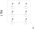
FIG. 3 andFIG. 4 . The switching unit may include a plurality of bridge arms electrically connected in series or in parallel. Various possible implementations of the switching unit are exemplified as follows, but the actual implementation of the switching unit is not limited thereto. The control unit corresponding to the switching unit can be referred toFIG. 5 andFIG. 6 , and the detailed descriptions thereof are omitted herein. - In an embodiment, the switching unit includes a plurality of bridge arms electrically connected in parallel, and each of the plurality of bridge arms is electrically connected to the DC-side capacitor C in parallel and includes a first switch and a second switch electrically connected in series. For example, as shown in
FIG. 7 , theswitching unit 11a includes three bridge arms electrically connected in parallel. The first bridge arm includes a first switch Q11 and a second switch Q21 electrically connected in series. The second bridge arm includes a first switch Q12 and a second switch Q22 electrically connected in series. The third bridge arm includes a first switch Q13 and a second switch Q23 electrically connected in series. - In an embodiment, the switching unit includes a plurality of bridge arms electrically connected in series, and each of the plurality of bridge arms includes a first switch and a second switch electrically connected in series. For example, as shown in
FIG. 8 , theswitching unit 11b includes two bridge arms connected in series. Each of the plurality of bridge arms is connected to a capacitor Cp in parallel, and the capacitors Cp corresponding to the plurality of bridge arms respectively are connected in series to form a DC side of theswitching unit 11b. The DC side formed by the capacitors Cp connected in series is electrically connected to the DC-side capacitor C in parallel. The first bridge arm includes a first switch Q14 and a second switch Q24 electrically connected in series. The second bridge arm includes a first switch Q15 and a second switch Q25 connected in series. The first switch Q14, the second switch Q24, the first switch Q15 and the second switch Q25 are serially connected in sequence. The second switch Q24 and the first switch Q15 are electrically connected to the midpoint between the two capacitors Cp. - In an embodiment, the switching unit includes a plurality of bridge arms connected in parallel, and each of the plurality of bridge arms includes two first switches and two second switches serially connected in sequence. Moreover, each of the plurality of bridge arms further includes a first diode and a second diode. A cathode of the first diode is electrically connected between the two first switches, an anode of the first diode is electrically connected to a cathode of the second diode, and an anode of the second diode is electrically connected between the two second switches. For example, as shown in
FIG. 9 , theswitching unit 11c includes two bridge arms electrically connected in parallel and two capacitors Cp. The two capacitors Cp are electrically connected in series to form a DC side of theswitching unit 11c, which is connected to the DC-side capacitor in parallel. The first bridge arm includes two first switches Q16 and Q17, two second switches Q26 and Q27, a first diode D1 and a second diode D2. The second bridge arm includes two first switches Q18 and Q19, two second switcher Q28 and Q29, a first diode D3 and a second diode D4. In the first bridge arm, the two first switches Q16 and Q17 and the two second switches Q26 and Q27 are connected in series between the input terminals. The cathode of the first diode D1 is electrically connected between the two first switches Q16 and Q17, and the anode of the first diode D1 is electrically connected to the cathode of the second diode D2 and a midpoint of the two capacitors Cp. The anode of the second diode D2 is electrically connected between the two second switches Q26 and Q27. In the second bridge arm, the two first switches Q18 and Q19 and the two second switches Q28 and Q29 are connected in series between input terminals. The cathode of the first diode D3 is electrically connected between the two first switches Q18 and Q19, and the anode of the first diode D3 is electrically connected to the cathode of the second diode D4 and a midpoint of the two capacitors. An anode of the second diode D4 is electrically connected between the two second switches Q28 and Q29. - Moreover, in addition to the aforementioned method of actively controlling the switching frequency for realizing the voltage equalization (active voltage equalizing), the cascaded conversion system of the present disclosure can also realize the voltage equalization through discharging the DC-side capacitor C in a passive manner. For example, the DC-side capacitor C may be discharged by a resistor. In an embodiment, as shown in
FIG. 10 , in each of the plurality ofconversion circuits 1, theconversion circuit 1 further includes a dischargingcircuit 16. The dischargingcircuit 16 includes a resistor R and a third switch Q3, and the dischargingcircuit 16 is electrically connected to two terminals of the DC-side capacitor C in parallel. When the third switch Q3 is turned on, the third switch Q3 and the resistor R discharge the DC-side capacitor C. - In an embodiment, the discharging
circuit 16 further includes a voltage equalizing control unit 161coupled to the DC-side capacitor C and the third switch Q3. The voltageequalizing control unit 161 controls the on and off of the third switch Q3 according to the voltage across the DC-side capacitor C. Specifically, when the voltage across the DC-side capacitor C is larger than the reference voltage, the voltageequalizing control unit 161 controls the third switch Q3 to be on. When the conversion circuit works in the above-mentioned active voltage equalizing state, the voltageequalizing control unit 161 controls the third switch Q3 to be off. - In an embodiment, the discharging
circuit 16 further includes afailure protection unit 162, and thefailure protection unit 162 is connected to the third switch Q3 in parallel. When the voltageequalizing control unit 161 or the third switch Q3 fails and breaks down, thefailure protection unit 162 and the resistor R discharge the DC-side capacitor C if the voltage across the DC-side capacitor C is larger than a failure voltage. The failure voltage represents the maximum voltage that the switches in theconversion circuit 1 are able to withstand. The DC-side capacitor C is set to be discharged when the voltage across the DC-side capacitor C is larger than the failure voltage, thus every component in theconversion circuit 1 can be protected from being damaged by overvoltage. - In an embodiment, the discharging
circuit 16 further includes adischarge control unit 163 connected to the third switch Q3. Thedischarge control unit 163 controls the third switch Q3 to be on when the cascaded conversion system works in a shutdown state so as to discharge the DC-side capacitor through the third switch Q3 and the resistor R. When a bus voltage of the cascaded conversion system is lower than a preset undervoltage protection value, or when the cascaded conversion system receives a shutdown command, the cascaded conversion system works in the shutdown state. - In an embodiment, the discharging
circuit 16 further includes afailure detection unit 164. Thefailure detection unit 164 is connected to the resistor R and detects the status of the resistor R (e.g., voltage, current, temperature, etc.) so as to determine whether the resistor R is overheated. Thefailure detection unit 164 warns when the resistor R is determined to be overheated. -
FIG. 11 is a schematic flow chart illustrating a voltage equalizing control method according to an embodiment of the present disclosure. The voltage equalizing control method is configured to control the cascaded conversion system of the above embodiments. As shown inFIG. 11 , the voltage equalizing control method includes steps S1 and S2. In the step S1, in eachconversion circuit 1, a driving signal including a switching frequency is generated according to the voltage across the DC-side capacitor C. In the step S2, the first switch and the second switch are controlled to be turned on alternately according to the driving signal, all the first switches are turned on and off simultaneously, and all the second switches are turned on and off simultaneously, thereby making the voltages across the DC-side capacitors C of all theconversion circuits 1 substantially equal. - In an embodiment, the voltage equalizing control method further includes a step of comparing the voltage across the DC-side capacitor with the reference voltage. In the case that the voltage across the DC-side capacitor C deviates from the reference voltage, the driving signal and the switching frequency are adjusted according to the comparison result when the
conversion circuit 1 works in the first state. - In this embodiment, the conversion circuit working in the first state means that the conversion circuit cannot output power, that is to say, the output power is extremely small or is even none. The first state is for example but not limited to a standby state (with a voltage at input and no voltage at output), a no-load state (with voltages at input and output and no load at output) and an extremely light-load state (with voltages at input and output and extremely small load at output).
- Under the circumstance that the conversion circuit includes the discharging circuit, in an embodiment, the voltage equalizing control method further includes steps of:
- when the voltage across the DC-side capacitor C being larger than the reference voltage, or when the cascaded conversion system working in the shutdown state, turning on the third switch Q3, thereby discharging the DC-side capacitor C by the third switch Q3 and the resistor R; and
- when the conversion circuit working in the above-mentioned active voltage equalizing state, turning off the third switch Q3.
- In an embodiment, the voltage equalizing control method further includes a step of: when the voltage across the DC-side capacitor C being larger than the failure voltage, utilizing the
failure protection unit 162 connected to the third switch Q3 in parallel and the resistor R to discharge the DC-side capacitor C. - From the above descriptions, the present disclosure provides a cascaded conversion system and a voltage equalizing control method thereof. The cascaded conversion system includes a plurality of conversion circuits electrically connected in cascade. Based on the principle that switching loss consumes electric power, the voltages across the capacitors of the plurality of conversion circuit can be adjusted through controlling the switching frequencies of the conversion circuits respectively. Accordingly, the voltages across the capacitors of all the conversion circuits can be adjusted to be equal, thereby equalizing the input voltage. Therefore, the cost and the occupied volume for realizing the input voltage equalization can be greatly reduced.
Claims (19)
- A cascaded conversion system, characterized by comprising:a plurality of conversion circuits (1) electrically connected in cascade, wherein each of the plurality of conversion circuits (1) comprises:a DC-side capacitor (C), wherein the DC-side capacitors (C) of the plurality of conversion circuits (1) are electrically connected in series;a switching unit (11) electrically connected to the DC-side capacitor (C) in parallel and comprising a plurality of bridge arms, wherein each of the plurality of bridge arms comprises a first switch (Q11) and a second switch (Q21); anda control unit (12) coupled to the switching unit (11) and the DC-side capacitor (C), wherein the control unit (12) is configured to output a driving signal (Vgsl, Vgs2, VgsN) having a switching frequency (fs) according to a voltage (VFB) across the DC-side capacitor (C) for controlling on and off of the switches (Q11, Q12, Q21, Q22) of the switching unit (11);wherein in each of the plurality of conversion circuits (1), the control unit (12) controls the first switch (Q11, Q12) and the second switch (Q21, Q22) to be turned on alternately with the switching frequency (fs) according to the driving signal (Vgsl, Vgs2, VgsN), and wherein in the plurality of bridge arms, all the first switches (Q11, Q12) are turned on and off simultaneously, all the second switches (Q21, Q22) are turned on and off simultaneously, thereby making the voltages (VFB1, VFB2, VFBn) across the DC-side capacitors (C) of the plurality of conversion circuits (1) equal.
- The cascaded conversion system according to claim 1, wherein in each of the plurality of conversion circuits (1), the conversion circuit (1) has a rated input voltage, there is a potential point between the first switch (Q11) and the second switch (Q21) of each of the plurality of bridge arms, and the voltage between the potential points of every two of the plurality of bridge arms is [0, 30%] times the rated input voltage.
- The cascaded conversion system according to claim 1, wherein the plurality of bridge arms in each switching unit (11) are electrically connected in parallel, and the first switch (Q11) and the second switch (Q21) in each of the plurality of bridge arms are electrically connected in series.
- The cascaded conversion system according to claim 1, wherein the plurality of bridge arms in each switching unit (11b) are electrically connected in series, and the first switch (Q14) and the second switch (Q24) in each of the plurality of bridge arms are electrically connected in series.
- The cascaded conversion system according to claim 1, wherein the plurality of bridge arms in each switching unit (11c) are electrically connected in parallel, each of the plurality of bridge arms comprises two first switches (Q16, Q17) and two second switches (Q26, Q27) serially connected in sequence, each of the plurality of bridge arms further comprises a first diode (D1) and a second diode (D2), a cathode of the first diode (D1) is electrically connected between the two first switches (Q16, Q17), an anode of the first diode (D1) is electrically connected to a cathode of the second diode (D2), and an anode of the second diode (D2) is electrically connected between the two second switches (Q26, Q27).
- The cascaded conversion system according to claim 1, wherein in each of the plurality of conversion circuits (1), the control unit (12) compares the voltage (VFB) across the DC-side capacitor (C) with a reference voltage (VREF) to obtain a comparison result, and the control circuit (12) adjusts the driving signal (Vgsl, Vgs2, VgsN) and the switching frequency (fs) according to the comparison result when the conversion circuit (1) is in a first state.
- The cascaded conversion system according to claim 6, wherein the first state is a standby state, a no-load state or an extremely light-load state.
- The cascaded conversion system according to claim 6, wherein the reference voltage (VREF) equals an input voltage received by the cascaded conversion system divided by the number of the conversion circuits (1), or equals an average value of the voltages (VFB1, VFB2, VFBn) across the DC-side capacitors (C) of the plurality of conversion circuits (1).
- The cascaded conversion system according to claim 6, wherein in each of the plurality of conversion circuits (1), the control unit (12) comprises a comparator (13), a controller (14) and a drive generator (15) connected in sequence, the comparator (13) receives and compares the reference voltage (VREF) with the voltage (VFB) across the DC-side capacitor (C), the comparator (13) outputs the comparison result to the controller (14), the controller (14) outputs the switching frequency (fs) to the drive generator (15) according to the comparison result, and the drive generator (15) outputs a plurality of driving signals (Vgsl, Vgs2, VgsN) according to the switching frequency (fs) for driving the switches in the switching unit (11) respectively.
- The cascaded conversion system according to claim 1, wherein in each of the plurality of conversion circuits (1), the conversion circuit (1) further comprises a discharging circuit (16), the discharging circuit (16) comprises a resistor (R) and a third switch (Q3), the discharging circuit (16) is electrically connected to two terminals of the DC-side capacitor (C) in parallel, and the third switch (Q3) and the resistor (R) discharge the DC-side capacitor (C) when the third switch (Q3) is turned on.
- The cascaded conversion system according to claim 10, wherein in each of the plurality of conversion circuits (1), the discharging circuit (16) further comprises a voltage equalizing control unit (161) coupled to the DC-side capacitor (C) and the third switch (Q3), the voltage equalizing control unit (161) controls the third switch (Q3) to be turned on when the voltage (VFB) across the DC-side capacitor (C) is larger than a reference voltage (VREF), wherein when all the first switches (Q11, Q12, Q13) are turned on and off simultaneously, and all the second switches (Q21, Q22, Q23) are turned on and off simultaneously, the voltage equalizing control unit (161) controls the third switch (Q3) to be turned off.
- The cascaded conversion system according to claim 11, wherein in each of the plurality of conversion circuits (1), the discharging circuit (16) further comprises a failure protection unit (162) electrically connected to the third switch (Q3) in parallel, and the failure protection unit (162) and the resistor (R) discharge the DC-side capacitor (C) when the voltage (VFB) across the DC-side capacitor (C) is larger than a failure voltage.
- The cascaded conversion system according to claim 10, wherein in each of the plurality of conversion circuits (1), the discharging circuit (16) further comprises a discharging control unit (163) connected to the third switch (Q3), and the discharging control unit (163) controls the third switch (Q3) to be turned on when the cascaded conversion system works in a shutdown state so as to discharge the DC-side capacitor (C) through the third switch (Q3) and the resistor (R).
- A voltage equalizing control method configured to control a cascaded conversion system, the cascaded conversion system comprising a plurality of conversion circuits (1) electrically connected in cascade, each of the plurality of conversion circuits (1) comprising a DC-side capacitor (C) and a switching unit (11), the DC-side capacitors (C) of the plurality of conversion circuits (11) being electrically connected in series, the switching unit (11) being electrically connected to the DC-side capacitor (C) in parallel and comprising a plurality of bridge arms, each of the plurality of bridge arms comprising a first switch (Q11) and a second switch (Q21), the voltage equalizing control method characterized by comprising:(a) in each of the plurality of conversion circuits (1), generating a driving signal (Vgsl, Vgs2, VgsN) having a switching frequency (fs) according to a voltage (VFB) across the DC-side capacitor (C); and(b) controlling the first switch (Q11) and the second switch (Q21) to be turned on alternately with the switching frequency (fs) according to the driving signal (Vgsl, Vgs2, VgsN), controlling all the first switches (Q11, Q12) to be turned on and off simultaneously, and controlling all the second switches (Q21, Q22) to be turned on and off simultaneously, thereby making the voltages (VFB1, VFB2, VFBn) across the DC-side capacitors (C) of the plurality of conversion circuits (1) equal.
- The voltage equalizing control method according to claim 14, further comprising: comparing the voltage (VFB) across the DC-side capacitor (C) with a reference voltage (VREF) to obtain a comparison result, and adjusting the driving signal (Vgsl, Vgs2, VgsN) and the switching frequency (fs) according to the comparison result when the conversion circuit (1) being in a first state.
- The voltage equalizing control method according to claim 15, wherein the first state is a standby state, a no-load state or an extremely light-load state.
- The voltage equalizing control method according to claim 15, wherein the reference voltage (VREF) equals an input voltage received by the cascaded conversion system divided by the number of the conversion circuits (1), or equals an average value of the voltages (VFB1, VFB2, VFBn) across the DC-side capacitors (C) of the plurality of conversion circuits (1).
- The voltage equalizing control method according to claim 14, wherein in each of the plurality of conversion circuits (1), the conversion circuit (1) further comprises a discharging circuit (16) comprising a resistor (R) and a third switch (Q3), the discharging circuit (16) is electrically connected to two terminals of the DC-side capacitor (C) in parallel, the voltage equalizing control method further comprising:when the voltage (VFB) across the DC-side capacitor (C) being larger than a reference voltage (VREF), or when the cascaded conversion system working in a shutdown state, turning on the third switch (Q3) for discharging the DC-side capacitor (C) through the third switch (Q3) and the resistor (R); andwhen all the first switches (Q11, Q12) being turned on and off simultaneously, and all the second switches (Q21, Q22) being turned on and off simultaneously, turning off the third switch (Q3).
- The voltage equalizing control method according to claim 18, further comprising: when the voltage (VFB) across the DC-side capacitor (C) being larger than a failure voltage, utilizing a failure protection unit (162) electrically connected to the third switch (Q3) in parallel and the resistor (R) to discharge the DC-side capacitor (C).
Applications Claiming Priority (1)
| Application Number | Priority Date | Filing Date | Title |
|---|---|---|---|
| CN202010995551.1A CN114257089A (en) | 2020-09-21 | 2020-09-21 | Cascade type conversion system and voltage-sharing control method thereof |
Publications (1)
| Publication Number | Publication Date |
|---|---|
| EP3972101A1 true EP3972101A1 (en) | 2022-03-23 |
Family
ID=77640420
Family Applications (1)
| Application Number | Title | Priority Date | Filing Date |
|---|---|---|---|
| EP21194742.9A Pending EP3972101A1 (en) | 2020-09-21 | 2021-09-03 | Modular conversion system with individual bridge outputs and stacked dc-link balancing by means of zero-vector switching |
Country Status (3)
| Country | Link |
|---|---|
| US (1) | US11515777B2 (en) |
| EP (1) | EP3972101A1 (en) |
| CN (1) | CN114257089A (en) |
Citations (5)
| Publication number | Priority date | Publication date | Assignee | Title |
|---|---|---|---|---|
| US20050284673A1 (en) * | 2004-06-08 | 2005-12-29 | Yosuke Nakazawa | Power source device for a vehicle |
| EP2148417A1 (en) * | 2008-07-22 | 2010-01-27 | SMA Solar Technology AG | Inverter apparatus for a photovoltaic generator with a plurality of inverters being serially coupled at their input side |
| EP2290799A1 (en) * | 2009-08-25 | 2011-03-02 | Converteam Technology Ltd | Bi-directional multilevel AC-DC converter arrangements |
| DE102012203073A1 (en) * | 2012-02-29 | 2013-08-29 | Zf Friedrichshafen Ag | Device for discharging intermediate circuit capacitor at high volt supply to supply electrical power to e.g. battery, has control unit for opening and closing switch while capacitor pole terminal is decoupled from load terminals |
| WO2019116722A1 (en) * | 2017-12-12 | 2019-06-20 | 株式会社日立製作所 | Power conversion device |
Family Cites Families (6)
| Publication number | Priority date | Publication date | Assignee | Title |
|---|---|---|---|---|
| DE112011105295B4 (en) | 2011-05-31 | 2017-02-09 | Toyota Jidosha Kabushiki Kaisha | Vehicle having an electric drive device and a discharge circuit and control method therefor |
| CN103944434B (en) | 2014-05-09 | 2016-06-29 | 北京四方继保自动化股份有限公司 | A kind of static state voltage equipoise system of chain type Multilevel Inverters power model |
| US10879805B2 (en) * | 2015-09-22 | 2020-12-29 | Infineon Technologies Austria Ag | System and method for a switched-mode power supply having a transformer with a plurality of primary windings |
| WO2018134827A1 (en) * | 2017-01-23 | 2018-07-26 | B.G. Negev Technologies And Applications Ltd., At Ben-Gurion University | System for balancing a series of cells |
| JP6822606B2 (en) * | 2018-12-17 | 2021-01-27 | 富士電機株式会社 | DC-DC converter device |
| CN113839561A (en) * | 2019-02-03 | 2021-12-24 | 台达电子工业股份有限公司 | DC/DC conversion system |
-
2020
- 2020-09-21 CN CN202010995551.1A patent/CN114257089A/en active Pending
-
2021
- 2021-09-02 US US17/465,434 patent/US11515777B2/en active Active
- 2021-09-03 EP EP21194742.9A patent/EP3972101A1/en active Pending
Patent Citations (6)
| Publication number | Priority date | Publication date | Assignee | Title |
|---|---|---|---|---|
| US20050284673A1 (en) * | 2004-06-08 | 2005-12-29 | Yosuke Nakazawa | Power source device for a vehicle |
| EP2148417A1 (en) * | 2008-07-22 | 2010-01-27 | SMA Solar Technology AG | Inverter apparatus for a photovoltaic generator with a plurality of inverters being serially coupled at their input side |
| EP2290799A1 (en) * | 2009-08-25 | 2011-03-02 | Converteam Technology Ltd | Bi-directional multilevel AC-DC converter arrangements |
| DE102012203073A1 (en) * | 2012-02-29 | 2013-08-29 | Zf Friedrichshafen Ag | Device for discharging intermediate circuit capacitor at high volt supply to supply electrical power to e.g. battery, has control unit for opening and closing switch while capacitor pole terminal is decoupled from load terminals |
| WO2019116722A1 (en) * | 2017-12-12 | 2019-06-20 | 株式会社日立製作所 | Power conversion device |
| US20210167690A1 (en) * | 2017-12-12 | 2021-06-03 | Hitachi Industrial Products, Ltd. | Power Conversion Device |
Also Published As
| Publication number | Publication date |
|---|---|
| US20220094257A1 (en) | 2022-03-24 |
| CN114257089A (en) | 2022-03-29 |
| US11515777B2 (en) | 2022-11-29 |
Similar Documents
| Publication | Publication Date | Title |
|---|---|---|
| US10044286B2 (en) | Power conversion system including plurality of power converters connected in parallel to load | |
| KR101538232B1 (en) | Battery Conditioning System and Battery Energy Storage System Including That Battery Conditioning System | |
| EP2020725A2 (en) | On-line uninterruptible power system | |
| EP1465318A2 (en) | Uninterruptible power supply system | |
| EP1450476B1 (en) | Power converter circuit | |
| US7023109B2 (en) | Uninterruptible power source apparatus | |
| JPH10234185A (en) | Power conversion device | |
| US10855197B2 (en) | Power supply system | |
| EP3972101A1 (en) | Modular conversion system with individual bridge outputs and stacked dc-link balancing by means of zero-vector switching | |
| JPH11113191A (en) | Uninterruptible power-supply apparatus and its charging control method | |
| EP2517345B1 (en) | Groundable dc/dc converter | |
| JP4370965B2 (en) | Power converter | |
| US7151678B2 (en) | Power system with redundant power supply apparatus | |
| CN109193918B (en) | Backup power supply, driving controller and electric automobile | |
| CN110783969B (en) | Battery Management System and Battery System | |
| RU2414788C1 (en) | Multi-channel uninterrupted power supply of modular construction | |
| WO2021028976A1 (en) | Power conversion apparatus | |
| CN112311221A (en) | Power converter and method for operating a power converter | |
| EP4145688A1 (en) | Power converter and control method thereof | |
| KR102475412B1 (en) | Power supply system of eletric vhiecle with fail safe function and fail safe method thereof | |
| CN113691119B (en) | Three-phase power factor correcting device | |
| KR102330697B1 (en) | Grid-connected energy storage system | |
| KR100507999B1 (en) | Chopper type voltage compensator with energy storage means | |
| CN116569459A (en) | DC voltage converter device, on-board electrical system for an electric vehicle, and method for operating a DC voltage converter device | |
| JP4147350B2 (en) | Uninterruptible power system |
Legal Events
| Date | Code | Title | Description |
|---|---|---|---|
| PUAI | Public reference made under article 153(3) epc to a published international application that has entered the european phase |
Free format text: ORIGINAL CODE: 0009012 |
|
| STAA | Information on the status of an ep patent application or granted ep patent |
Free format text: STATUS: THE APPLICATION HAS BEEN PUBLISHED |
|
| AK | Designated contracting states |
Kind code of ref document: A1 Designated state(s): AL AT BE BG CH CY CZ DE DK EE ES FI FR GB GR HR HU IE IS IT LI LT LU LV MC MK MT NL NO PL PT RO RS SE SI SK SM TR |
|
| STAA | Information on the status of an ep patent application or granted ep patent |
Free format text: STATUS: REQUEST FOR EXAMINATION WAS MADE |
|
| 17P | Request for examination filed |
Effective date: 20220923 |
|
| RBV | Designated contracting states (corrected) |
Designated state(s): AL AT BE BG CH CY CZ DE DK EE ES FI FR GB GR HR HU IE IS IT LI LT LU LV MC MK MT NL NO PL PT RO RS SE SI SK SM TR |