JP4147724B2 - ANTENNA DEVICE AND RADIO DEVICE - Google Patents
ANTENNA DEVICE AND RADIO DEVICE Download PDFInfo
- Publication number
- JP4147724B2 JP4147724B2 JP2000174309A JP2000174309A JP4147724B2 JP 4147724 B2 JP4147724 B2 JP 4147724B2 JP 2000174309 A JP2000174309 A JP 2000174309A JP 2000174309 A JP2000174309 A JP 2000174309A JP 4147724 B2 JP4147724 B2 JP 4147724B2
- Authority
- JP
- Japan
- Prior art keywords
- frequency
- dielectric substrate
- frequency band
- main surface
- dielectric
- Prior art date
- Legal status (The legal status is an assumption and is not a legal conclusion. Google has not performed a legal analysis and makes no representation as to the accuracy of the status listed.)
- Expired - Fee Related
Links
Images


Classifications
-
- H—ELECTRICITY
- H01—ELECTRIC ELEMENTS
- H01Q—ANTENNAS, i.e. RADIO AERIALS
- H01Q21/00—Antenna arrays or systems
- H01Q21/06—Arrays of individually energised antenna units similarly polarised and spaced apart
- H01Q21/061—Two dimensional planar arrays
- H01Q21/065—Patch antenna array
-
- H—ELECTRICITY
- H01—ELECTRIC ELEMENTS
- H01Q—ANTENNAS, i.e. RADIO AERIALS
- H01Q1/00—Details of, or arrangements associated with, antennas
- H01Q1/12—Supports; Mounting means
- H01Q1/22—Supports; Mounting means by structural association with other equipment or articles
- H01Q1/24—Supports; Mounting means by structural association with other equipment or articles with receiving set
- H01Q1/241—Supports; Mounting means by structural association with other equipment or articles with receiving set used in mobile communications, e.g. GSM
- H01Q1/242—Supports; Mounting means by structural association with other equipment or articles with receiving set used in mobile communications, e.g. GSM specially adapted for hand-held use
- H01Q1/243—Supports; Mounting means by structural association with other equipment or articles with receiving set used in mobile communications, e.g. GSM specially adapted for hand-held use with built-in antennas
-
- H—ELECTRICITY
- H01—ELECTRIC ELEMENTS
- H01Q—ANTENNAS, i.e. RADIO AERIALS
- H01Q3/00—Arrangements for changing or varying the orientation or the shape of the directional pattern of the waves radiated from an antenna or antenna system
- H01Q3/26—Arrangements for changing or varying the orientation or the shape of the directional pattern of the waves radiated from an antenna or antenna system varying the relative phase or relative amplitude of energisation between two or more active radiating elements; varying the distribution of energy across a radiating aperture
- H01Q3/2605—Array of radiating elements provided with a feedback control over the element weights, e.g. adaptive arrays
-
- H—ELECTRICITY
- H01—ELECTRIC ELEMENTS
- H01Q—ANTENNAS, i.e. RADIO AERIALS
- H01Q9/00—Electrically-short antennas having dimensions not more than twice the operating wavelength and consisting of conductive active radiating elements
- H01Q9/04—Resonant antennas
- H01Q9/0407—Substantially flat resonant element parallel to ground plane, e.g. patch antenna
Description
【0001】
【発明の属する技術分野】
本発明は、複数の周波数に対して等価利得を得るアンテナ装置及びこのアンテナ装置を搭載することにより周波数帯域を異にする複数の無線通信システムにも適用される無線装置に関する。
【0002】
【従来の技術】
無線通信システム、例えば携帯電話システムにおいては、近年驚異的な普及とともに通話サービスばかりでなく電子メール等の文字情報の伝送サービスが行われるようになっている。携帯電話システムにおいては、例えば着信メロディのダウンロードサービス或いはキャラクタ配信サービス等が好評を博しており、さらに電子商取引、楽音配給等の種々の新たなサービスの展開が図られている。携帯電話システムにおいては、様々な形態の情報をより多く高速かつ高品質で伝送する種々の対応が図られており、将来的には高品質の動画情報もリアルタイムに送受信可能とされるようになる。
【0003】
携帯電話システムにおいては、国内でも例えば高速化等の対応に伴う新たなシステムとして、IMT−2000(International Mobile Telecommunication-2000)に準拠したサービスの開始が予定されている。同システムにおいては、新たな周波数帯域(2Ghz帯)が割り当てられ、伝送スピードが既存方式の64kビット/秒に対して、当面384kビット/秒のサービス提供が可能となる。携帯電話システムにおいては、新たな周波数帯域においても、各種の情報信号を受信可能とする機器を必要とする。
【0004】
無線通信システムにおいては、それぞれについて使用周波数帯域が定められており、限られた周波数帯域を有効に利用することが必要である。無線通信システムにおいては、使用機器が所望の電波のみを受信して妨害となる他の電波を受信しないように構成されることによって、多くの機器が有効に使用することを可能とすることが必要である。無線通信システムにおいては、例えば使用機器に、図6乃至図8に示すアダプティブアレィアンテナ装置100を搭載することによってその対応が図られる。
【0005】
アダプティブアレィアンテナ装置100は、図6に示すように、空間的に配置される複数のアンテナ素子101と、各アンテナ素子101で受信した高周波信号をそれぞれ復調する複数の受信回路部102と、各受信回路部102において復調した信号を最適化する並列信号処理部103とを備えて構成される。アダプティブアレィアンテナ装置100は、異なる方向から到来する高周波信号を各アンテナ素子101によって同時に受信したり、妨害となる高周波信号を遮断する。
【0006】
各受信回路部102は、各アンテナ素子101によって受信した高周波信号をそれぞれダウンコンバートしてビット信号に復調する。並列信号処理部103は、受信回路部102から供給されたビット信号を最適に合成する。アダプティブアレィアンテナ装置100は、並列信号処理部103において必要となる情報以外の情報や雑音を打ち消すようにビット信号の合成を行うことで、あたかもアンテナの指向性が必要となる電波の方向を向き、妨害電波の来る方向に対してヌルとなるように動作する。
【0007】
また、アダプティブアレィアンテナ装置100は、並列信号処理部103からの出力を複数用意することによって、必要とする情報が2種類以上ある場合においてもそれぞれの情報が別々に出力されるように構成される。したがって、アダプティブアレィアンテナ装置100は、必要とする情報の数に合わせて複数の指向性を有して動作する特性を有している。アダプティブアレィアンテナ装置100は、同じ周波数帯域を用いた情報が同一空間に複数存在する場合においても、互いに混信を生じることなくそれぞれの情報の受信を可能として周波数帯域の有効利用を図るようにするといった特徴を有している。
【0008】
アンテナ素子101は、図7及び図8に示すようにテフロン(商品名:デュポン社)等からなる矩形状の誘電体基板104と、この誘電体基板104の第1の主面104aに設けられたグランド導体105と、誘電体基板104の第2の主面104bにそれぞれ接合された複数の放射導体106と、グランド導体105と各放射導体106とを接続する給電線107とから構成される。誘電体基板104は、比誘電率がε0であり、図8に示すように第1の主面104aと第2の主面104bとを貫通して複数の給電ガイド孔108が形成されている。
【0009】
グランド導体105は、例えば銅や黄銅等の金属板からなり、上述したように誘電体基板104の第1の主面104a上に接合されるとともに底面部に各受信回路部102が配置されている。放射導体106は、グランド導体105と平行な状態を保持されて誘電体基板104の第2の主面104bに接合されている。放射導体106は、例えば銅や黄銅等の金属チップ片からなり、1辺の長さをLとしたほぼ正方形を呈している。放射導体106は、送受信波の波長をλとしたとき、1辺の長さLがλ/2に設定される。また、放射導体106は、1辺の長さLが、通信周波数をf0、光速をcとすると、
2L=c/(f0×√ε0)
により設定される。
【0010】
給電線107には、同軸ケーブルが用いられ、給電ガイド孔108を貫通されることによって各放射導体106と対応する受信回路部102とをそれぞれ接続する。給電線107は、詳細を省略するが外殻導体がグランド導体105と接続されるとともに、芯線が放射導体106と接続されている。
【0011】
以上のように構成されたアダプティブアレィアンテナ装置100は、図8に示すように異なる方向から送信された同一周波数帯域の高周波信号109(109a、109b、109c)を、各アンテナ素子101によって受信する。アダプティブアレィアンテナ装置100は、各アンテナ素子101に対応した各受信回路部102において、高周波信号109をそれぞれダウンコンバートしてビット信号に復調する。アダプティブアレィアンテナ装置100は、図6に示すように各受信回路部102から供給されたビット信号について、並列信号処理部103において必要となる情報以外の情報や雑音を打ち消すように合成を行ってそれぞれ出力する。
【0012】
【発明が解決しようとする課題】
無線通信システムにおいては、上述したように異なる周波数帯域を使用する複数システムが提供されるようになり、使用機器もそれぞれのシステムに対応したものが必要となる。使用機器は、例えば各無線通信システムに共用可能とする場合に、各システムに適合した複数のアンテナ装置が必要となり大型化するとともに高価となってしまう。
【0013】
携帯電話システムは、小型、軽量化、廉価な携帯電話機の提供等も大きな要因として驚異的な普及が図られた経緯もあることから、上述した新たな携帯電話システムの導入に伴って携帯電話機が大型化、高価となる対応を図ることはできない。したがって、新たな携帯電話システムには、従来と互換性の無い携帯電話機が提供されるといった問題がある。
【0014】
従来のアダプティブアレィアンテナ装置は、上述したように同一周波数帯域において指向性を制御することによって周波数の有効利用を可能とする。かかるアダプティブアレィアンテナ装置においても、周波数帯域を異にする複数システムに適用する場合には、その他のアンテナ装置と同様に各システムの仕様にそれぞれ適合した複数が用いられなければならない。
【0015】
したがって、本発明は、上述したアダプティブアレィアンテナ装置の特性に着目し、複数の周波数帯域においても必要な情報を確実に受信可能とすることによって限られた周波数帯域の有効利用が図られるようにしたアンテナ装置及び無線装置を提供することを目的に提案されたものである。
【0016】
【課題を解決するための手段】
上述した目的を達成する本発明にかかるアンテナ装置は、比誘電率εnが周波数分散特性を有する誘電体材料からなる誘電体基板と、この誘電体基板の第1主面に形成されたグランド導体と、誘電体基板の第2主面に形成された一辺の長さをL(L=λ/2 但し、λは通信周波数帯域信号の波長)とした正方形からなる複数の放射導体と、誘電体基板を貫通して形成されグランド導体と放射導体とを接続する複数の給電線とを備える。アンテナ装置は、誘電体基板がその比誘電率εnを、
2L=c/(f1×√ε1)=c/(f2×√ε2)=c/(f3×√ε3)・・・= c/(fn×√εn)(但し、通信周波数fn(n≧2)、光速c)
となる周波数分散特性を有する誘電体材料により形成され、複数の通信周波数に対して等価利得を得る。
【0017】
以上のように構成された本発明にかかるアンテナ装置によれば、異なる方向から到来する高周波信号を同時に受信したり、妨害となる高周波信号を遮断する。また、アンテナ装置によれば、周波数を異にする高周波信号を受信すると、誘電体基板の周波数分散特性により同一波長の出力を得て各周波数毎の分配を行う。したがって、アンテナ装置によれば、周波数帯域を異にする無線通信システムへの適用が可能とされるとともに、周波数の有効利用が図られるようにする。
【0018】
また、上述した目的を達成する本発明にかかる無線装置は、複数の平面アンテナと、複数の周波数信号処理部と、複数の出力部及び/又は入力部と、これら各部の動作を制御するシステム制御部とを備える。無線装置は、平面アンテナが、比誘電率εnが周波数分散特性を有する誘電体材料からなる誘電体基板と、この誘電体基板の第1主面に形成されたグランド導体と、誘電体基板の第2主面に形成された一辺の長さをLとした正方形からなりアレィ状に配置された複数の放射導体と、誘電体基板を貫通して形成されてグランド導体と放射導体とを接続する複数の給電線とを備える。平面アンテナは、誘電体基板が、その比誘電率εnを2L=c/(f1×√ε1)=c/(f2×√ε2)=c/(f3×√ε3)・・・=c/(fn×√εn)(但し、通信周波数fn(n≧2)、光速c)となる周波数分散特性を有する誘電体材料からなり、複数の通信周波数に対して等価利得を得る。無線装置は、各周波数信号処理部が、各平面アンテナによりそれぞれ受信した複数の通信周波数帯域信号及び/又は送信する複数の通信周波数帯域信号を周波数帯域毎にそれぞれ分配して処理する。無線装置は、各出力部が各周波数信号処理部からの出力を処理するとともに、各入力部が各周波数信号処理部への入力を処理する。
【0019】
以上のように構成された本発明にかかる無線装置によれば、平面アンテナにより、異なる方向から到来する高周波信号を同時に受信するとともに、周波数を異にする高周波信号についてもこれを受信して誘電体基板の周波数分散特性によって同一波長の出力を得て各周波数毎に分配する。無線装置によれば、分配した高周波信号をそれぞれ対応する受信回路部においてダウンコンバートしてビット信号に復調する。無線装置によれば、各受信回路部から供給されたビット信号を並列信号処理回路部において最適に合成して出力する。無線装置によれば、単一のアンテナ装置によって周波数帯域の異なる複数のシステムから送信される複数の情報を混信を生じることなく送受信することが可能とされ、大型化することなく周波数の有効活用が図られるようになる。
【0020】
【発明の実施の形態】
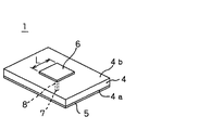
以下、本発明の実施の形態について、図面を参照して詳細に説明する。実施の形態として図1に示した平面アンテナ1は、複数個が図3及び図4に示すように互いに隣接されて配置されてアンテナ素子を構成する。アダプティブアンテナアレィ装置2は、図5に示した無線装置3に備えられ、異なる方向から送信される異なる周波数帯域の高周波信号を受信するとともに異なる周波数帯域の高周波信号を送信する送受信部を構成する。
【0021】
平面アンテナ1は、基本的な構成を従来の平面アンテナとほぼ同様とし、図1に示すように、矩形状の誘電体基板4と、この誘電体基板4の第1の主面4aに設けられたグランド導体5と、誘電体基板4の第2の主面4bにそれぞれ接合された複数の放射導体6とを備えている。平面アンテナ1は、誘電体基板4に形成した給電ガイド孔8に同軸ケーブルからなる給電線7が貫通され、この給電線7によりグランド導体5と各放射導体6とが接続される。給電線7は、外殻導体がグランド導体5に接続されるとともに、芯線が放射導体6と接続される。
【0022】
グランド導体5は、例えば黄銅等の金属板によって形成され、上述したように誘電体基板4の第1の主面4a上に接合されている。放射導体6は、グランド導体105と平行な状態を保持されて誘電体基板4の第2の主面4b上に接合されている。放射導体6は、例えば黄銅等の金属チップ片からなり、1辺の長さをLとしたほぼ正方形を呈している。放射導体6は、送受信波の波長をλとしたときに、1辺の長さLがλ/2に設定される。
【0023】
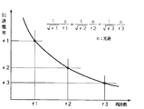
誘電体基板4は、比誘電率が周波数分散特性を有する誘電体材料によって成形されており、放射導体6の1辺の長さLと各周波数f1乃至fnとに対する比誘電率ε1乃至εnが、図2に示すように周波数が大きくなるにしたがって次第に小さくなるような周波数特性を有してなる。誘電体基板4は、比誘電率ε1乃至εnが、
2L=c/(f1×√ε1)=c/(f2×√ε2)=c/(f3×√ε3)・・・=c/(fn×√εn)
となる特性を有することにより、複数の受信周波数f1乃至fnに対して同一波長の出力を得るようにする。
【0024】
かかる誘電体基板4は、例えば組成が、
BaFe12−2xMe1xMe2xO19
SrFe12−2xMe1xMe2xO19
で示される六方晶フェライト材によって成形される。なお、Me1は、例えばTi、Zr、Sn等の4価の金属イオンである。また、Me2は、Co、Mn、Zn、Cu、Mg、Ni等の2価の金属イオンである。
【0025】
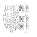
アダプティブアレィアンテナ装置2は、上述した平面アンテナ1をアンテナ素子として備えることによって、例えば第1の周波数帯域f1と、第2の周波数帯域f2と、第3の周波数帯域f3とを同時に受信可能とする。アダプティブアレィアンテナ装置2は、図3に示すように誘電体基板4の第1の主面4a上に複数個の放射導体6(6a乃至6n)をアレィ配置してなる平面アンテナ10(10a乃至10n)を備える。
【0026】
アダプティブアレィアンテナ装置2は、図4に示すように、各平面アンテナ10にそれぞれ対応して複数の周波数分配回路部11(11a乃至11n)を備える。各周波数分配回路部11は、図3に示すように給電線7(7a乃至7n)を介して対応する各平面アンテナ10と接続されている。各周波数分配回路部11は、平面アンテナ10によって受信した例えば3種類の高周波信号16乃至18を第1の周波数帯域f1乃至第3の周波数帯域f3毎に分配する。
【0027】
アダプティブアレィアンテナ装置2は、図3及び図4に示すように、各周波数分配回路部11にそれぞれ対応して複数の受信回路部12(12a乃至12n)を備える。各受信回路部12は、図4に示すように、それぞれ第1の周波数帯域f1乃至第3の周波数帯域f3の高周波信号16乃至18毎に対応する3組の要素受信回路部13(第1の要素受信回路部13a1乃至第3の要素受信回路部13a3)・・・(第1の要素受信回路部13n1乃至第3の要素受信回路部13n3)とからなる。各受信回路部12は、各周波数分配回路部11によって分配された第1の周波数帯域f1乃至第3の周波数帯域f3毎の高周波信号16乃至18をベースバウンド信号にダウンコンバートしてビット信号に復調する。
【0028】
アダプティブアレィアンテナ装置2は、図4に示すように、受信回路部12の各要素受信回路部13から第1の周波数帯域f1乃至第3の周波数帯域f3毎のビット信号が供給される3個の並列信号処理部14(第1の並列信号処理部14a乃至第3の並列信号処理部14c)を備える。各並列信号処理部14は、第1の周波数帯域f1乃至第3の周波数帯域f3毎にビット信号を最適に合成する。各並列信号処理部14は、必要となる情報以外の情報や雑音を打ち消すように各周波数帯域毎のビット信号の合成を行うことで、あたかもアンテナの指向性が必要となる電波の方向を向き、妨害電波の来る方向に対してヌルとなるように動作する。各並列信号処理部14は、最適化したビット信号を受信信号19a〜19n、20a〜20n、21a〜21nとして第1の周波数帯域f1乃至第3の周波数帯域f3にそれぞれ対応したシステム部15(第1のシステム部15a乃至第3のシステム部c)へと出力する。
【0029】
アダプティブアレィアンテナ装置2は、図3に示すように、第1の周波数帯域f1を使用した無線通信システムによって異なる方向から送信された複数の第1の高周波信号16(16a乃至16c:同図実線)を、アレィ配置された平面アンテナ10によって受信する。アダプティブアレィアンテナ装置2は、第2の周波数帯域f2を使用した無線通信システムによって異なる方向から送信された複数の第2の高周波信号17(17a乃至17c:同図破線)を、アレィ配置された平面アンテナ10によって受信する。アダプティブアレィアンテナ装置2は、第3の周波数帯域f3を使用した無線通信システムによって異なる方向から送信された複数の第3の高周波信号18(18a乃至18c:同図鎖線)を、アレィ配置された平面アンテナ10によって受信する。
【0030】
アダプティブアレィアンテナ装置2は、上述したように各平面アンテナ10が比誘電率εに周波数分散性を有する誘電体基板4を備えることから、第1の高周波信号16乃至第3の高周波信号18について同一波長の高周波信号として受信する。アダプティブアレィアンテナ装置2は、各平面アンテナ10によって受信した第1の高周波信号16乃至第3の高周波信号18を、各周波数分配回路部11によって第1の周波数帯域f1乃至第3の周波数帯域f3毎に受信回路部12の各要素受信回路部13にそれぞれ分配する。アダプティブアレィアンテナ装置2は、各要素受信回路部13において高周波信号をビット信号に復調して並列信号処理部14へと出力する。
【0031】
アダプティブアレィアンテナ装置2においては、例えば平面アンテナ10aによって受信され第1の周波数分配回路部11aにより分配された第1の周波数帯域f1に基づく第1の高周波信号16aを、受信回路部12の第1の要素受信回路部13a1においてビット信号に復調して、第1の並列信号処理部14aへと出力する。アダプティブアレィアンテナ装置2においては、例えば平面アンテナ10aによって受信され第1の周波数分配回路部11aにより分配された第2の周波数帯域f2に基づく第2の高周波信号17aを、受信回路部12の第2の要素受信回路部13a2においてビット信号に復調して、第2の並列信号処理部14bへと出力する。アダプティブアレィアンテナ装置2においては、例えば平面アンテナ10aによって受信され第1の周波数分配回路部11aにより分配された第3の周波数帯域f3に基づく第3の高周波信号18aを、受信回路部12の第3の要素受信回路部13a3においてビット信号に復調し、第3の並列信号処理部14cへと出力する。
【0032】
アダプティブアレィアンテナ装置2は、例えば平面アンテナ10bによって受信され第2の周波数分配回路部11bにより分配された第1の周波数帯域f1に基づく第1の高周波信号16bを、受信回路部12bの第2の要素受信回路部13b1においてビット信号に復調して、第1の並列信号処理部14aへと出力する。アダプティブアレィアンテナ装置2は、例えば平面アンテナ10nによって受信され第nの周波数分配回路部11nにおいて分配された第1の周波数帯域f1に基づく第1の高周波信号16nを、受信回路部12の第nの要素受信回路部13n1においてビット信号に復調して、第1の並列信号処理部14aへと出力する。
【0033】
アダプティブアレィアンテナ装置2は、異なる方向から送信され各平面アンテナ10によって同時に受信した第1の周波数帯域f1に基づく第1の高周波信号16を上述した経路を経て第1の並列信号処理部14aにおいて最適化処理した後に、受信情報19a乃至19nとして第1の周波数帯域システム部22aに出力する。アダプティブアレィアンテナ装置2は、異なる方向から送信され各平面アンテナ10によって同時に受信した第2の周波数帯域f2に基づく第2の高周波信号17を上述した経路を経て第2の並列信号処理部14bにおいて最適化処理した後に、受信情報20a乃至20nとして第2の周波数帯域システム部22bに出力する。アダプティブアレィアンテナ装置2は、異なる方向から送信され各平面アンテナ10によって同時に受信した第3の周波数帯域f3に基づく第3の高周波信号18を上述した経路を経て第3の並列信号処理部14cにおいて最適化処理した後に、受信情報21a乃至21nとして第2の周波数帯域システム部22cに出力する。
【0034】
アダプティブアレィアンテナ装置2は、上述したように異なる周波数帯域f1乃至f3に基づく複数の高周波信号16乃至18が異なる方向から送信された場合においても、これらを混信を生じることなく受信する。したがって、アダプティブアレィアンテナ装置2は、同一周波数帯域ばかりでなく異なる周波数帯域においても互換性を有して情報受信を可能とすることで、アンテナ部を大型化することなく周波数の有効利用が図られるようにする。
【0035】
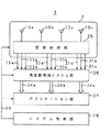
無線装置3は、図5に示すように上述したアダプティブアレィアンテナ装置2を搭載することによって、異なる周波数帯域を使用する無線通信システムに用いることが可能とされる。無線装置3は、複数の平面アンテナ10によって異なる方向から送信された異なる周波数帯域f1乃至f3に基づく複数の高周波信号16乃至18を混信することなく受信して、受信処理部25において最適な処理を施す。受信処理部25は、上述した周波数分配回路部11や受信回路部12或いは並列信号処理部14等から構成される。
【0036】
無線装置3は、受信処理部25から上述したように各周波数帯域f1乃至f3毎に最適化処理が施された受信情報19乃至21が周波数帯域システム部26にそれぞれ出力される。無線装置3は、周波数帯域システム部26において、付設された表示部やメモリ等のアプリケーション部27を適宜制御する制御信号処理を施して、各周波数帯域f1乃至f3に対応した制御信号24a乃至24cを出力する。無線装置3は、制御信号24a乃至24cに基づいてアプリケーション部27の各部において所定の動作が行われる。
【0037】
無線装置3は、アダプティブアレィアンテナ装置2や周波数帯域システム部26或いはアプリケーション部27が、システム制御部28から出力される制御信号29によって制御される。システム制御部28は、各周波数帯域f1乃至f3の対応、通信方式の対応、信号処理或いはアプリケーション制御をソフトウェアプログラムによって制御して制御信号29を出力する。換言すれば、無線装置3は、全体の動作がソフトウェアプログラムによって制御される。
【0038】
なお、上述した実施の形態においては、第1の周波数帯域f1乃至第3の周波数帯域f3に基づく第1の高周波信号16乃至第3の高周波信号18の受信動作について説明したが、本発明は送信部に接続して用いることも可能であることは勿論である。実施の形態においては、誘電体基板4が六方晶フェライトによって成形されて周波数分散特性を付与するようにしたが、かかる材料に限定されるものではないことは勿論である。
【0039】
実施の形態においては、放射導体6に矩形チップ片のいわゆる方形パッチ素子を用いたが、かかる素子に限定されるものではないことは勿論である。放射導体6は、例えば線状素子からなりこれを格子状に組み合わせたり、誘電体基板4の表面に貼着した金属箔をエッチング処理等を施して形成するようにしてもよい。
【0040】
【発明の効果】
以上詳細に説明したように、本発明にかかるアンテナ装置によれば、比誘電率を周波数分散特性を有する誘電体材料によって形成された誘電体基板を備えて、複数の周波数に対して等価利得を得るように構成したこから、異なる方向から到来する高周波信号を同時に受信したり妨害となる高周波信号を遮断するとともに周波数を異にする高周波信号も混信を生じることなく送受信を可能とする。したがって、アンテナ装置によれば、周波数帯域を異にする無線通信システムへの適用が可能とされるとともに、周波数の有効利用を図るようにする。
【0041】
また、本発明にかかる無線装置によれば、誘電体基板が比誘電率に周波数分散特性を有し複数の周波数に対して等価利得を得る誘電体材料によって形成されてなる平面アンテナを搭載することで、この平面アンテナによって異なる方向から到来する高周波信号を同時に受信するとともに、周波数を異にする高周波信号についてもこれを受信する。無線装置によれば、単一のアンテナ装置によって周波数帯域の異なる複数の無線通信システムから送信される複数の情報を混信を生じることなく送受信することから、複数の無線通信システムに対して互換性を有して接続が可能とされるとともに小型化が図られかつ限られた周波数帯域の有効活用を図るようにする。
【図面の簡単な説明】
【図1】 本発明の実施の形態として示す平面アンテナの斜視図である。
【図2】 同平面アンテナに備えられる誘電体基板の比誘電率の特性図である。
【図3】 同平面アンテナをアンテナ素子として用いたアダプティブアレィアンテナ装置の受信部の構成説明図である。
【図4】 同アダプティブアレィアンテナ装置の概略構成図である。
【図5】 同アダプティブアレィアンテナ装置を備えた無線装置の概略構成図である。
【図6】 従来のアダプティブアレィアンテナ装置の概略構成図である。
【図7】 同アダプティブアレィアンテナ装置にアンテナ素子として用いられる平面アンテナの斜視図である。
【図8】 同アダプティブアレィアンテナ装置の受信部の構成説明図である。
【符号の説明】
1平面アンテナ、2 アダプティブアレィアンテナ装置、3 無線装置、4 誘電体基板、5 グランド導体、6 放射導体、7 給電線、10平面アンテナ、11 周波数分配回路部、12 受信回路部、13 要素受信回路部、14 並列信号処理部、15 システム部、16〜18 高周波信号、19〜21 受信信号、22 周波数帯域システム部、24 制御信号、25 受信処理部、26 周波数帯域システム部、27 アプリケーション部、28 システム制御部、29 制御信号[0001]
BACKGROUND OF THE INVENTION
The present invention relates to an antenna device that obtains an equivalent gain for a plurality of frequencies and a wireless device that is also applied to a plurality of wireless communication systems that have different frequency bands by mounting the antenna device.
[0002]
[Prior art]
2. Description of the Related Art In recent years, wireless communication systems, for example, mobile phone systems, have been used not only for calling services but also for character information transmission services such as e-mails as a result of tremendous spread. In the mobile phone system, for example, a ringtone melody download service or a character distribution service is gaining popularity, and various new services such as electronic commerce and music distribution are being developed. In mobile phone systems, various measures for transmitting various forms of information at a higher speed and with higher quality have been made, and in the future, high-quality moving picture information can be transmitted and received in real time. .
[0003]
In the cellular phone system, a service based on IMT-2000 (International Mobile Telecommunication-2000) is scheduled to start as a new system in response to, for example, speeding up in Japan. In this system, a new frequency band (2 Ghz band) is allocated, and it becomes possible to provide a service with a transmission speed of 384 kbit / sec for the time being compared with the existing scheme of 64 kbit / sec. A cellular phone system requires a device that can receive various information signals even in a new frequency band.
[0004]
In the wireless communication system, the frequency band to be used is determined for each, and it is necessary to effectively use the limited frequency band. In a wireless communication system, it is necessary to enable many devices to use effectively by using the device to receive only desired radio waves and not receiving other radio waves that may interfere. It is. In the wireless communication system, for example, the adaptive
[0005]
As shown in FIG. 6, the adaptive
[0006]
Each
[0007]
In addition, the adaptive
[0008]
As shown in FIGS. 7 and 8, the
[0009]
The
2L = c / (f0 × √ε0)
Is set by
[0010]
A coaxial cable is used as the
[0011]
The adaptive
[0012]
[Problems to be solved by the invention]
In the wireless communication system, as described above, a plurality of systems using different frequency bands are provided, and devices used for each system are required. For example, when the equipment used can be shared by each wireless communication system, a plurality of antenna devices suitable for each system are required, which increases the size and cost.
[0013]
Since the mobile phone system has been used astoundingly due to factors such as the provision of a small, lightweight, and inexpensive mobile phone, the mobile phone system has been introduced along with the introduction of the new mobile phone system described above. Larger and more expensive measures cannot be taken. Therefore, the new mobile phone system has a problem that a mobile phone that is not compatible with the conventional one is provided.
[0014]
The conventional adaptive array antenna apparatus has directivity in the same frequency band as described above.To controlByAroundEnables effective use of wavenumbers. Also in such an adaptive array antenna apparatus, when applied to a plurality of systems having different frequency bands, a plurality conforming to the specifications of each system must be used in the same manner as other antenna apparatuses.
[0015]
Therefore, the present invention pays attention to the characteristics of the above-described adaptive array antenna device so that necessary information can be reliably received even in a plurality of frequency bands so that limited frequency bands can be effectively used. The present invention has been proposed for the purpose of providing an antenna device and a wireless device.
[0016]
[Means for Solving the Problems]
The antenna device according to the present invention that achieves the above-described object is as follows.A dielectric substrate made of a dielectric material having a relative dielectric constant εn having frequency dispersion characteristics, a ground conductor formed on the first main surface of the dielectric substrate, and one side formed on the second main surface of the dielectric substrate A plurality of square radiating conductors with a length of L (L = λ / 2, where λ is the wavelength of the communication frequency band signal), and a ground conductor and the radiating conductor formed through the dielectric substrate are connected. A plurality of feeder lines. In the antenna device, the dielectric substrate has a relative dielectric constant εn,
2L = c / (f1 × √ε1) = c / (f2 × √ε2) = c / (f3 × √ε3). c / (fn × √εn) (however, communication frequency fn (n ≧ 2), speed of light c)
It is formed of a dielectric material having a frequency dispersion characteristic to obtain an equivalent gain for a plurality of communication frequencies.
[0017]
According to the antenna device according to the present invention configured as described above, high-frequency signals arriving from different directions are received at the same time or high-frequency signals that are obstructive are blocked. Also, according to the antenna device, when receiving a high frequency signal having a different frequency, an output of the same wavelength is obtained by the frequency dispersion characteristic of the dielectric substrate, and distribution is performed for each frequency. Therefore, according to the antenna device, it is possible to apply to a radio communication system having different frequency bands and to effectively use the frequency.
[0018]
A wireless device according to the present invention that achieves the above-described object isA plurality of planar antennas, a plurality of frequency signal processing units, a plurality of output units and / or input units, and a system control unit that controls operations of these units. In the wireless device, the planar antenna includes a dielectric substrate made of a dielectric material having a relative dielectric constant εn having frequency dispersion characteristics, a ground conductor formed on the first main surface of the dielectric substrate, and a first dielectric substrate. (2) A plurality of radiating conductors that are formed in an array and are formed in a square shape with one side length L formed on the principal surface, and a plurality that are formed through the dielectric substrate and connect the ground conductor and the radiating conductor. Power supply line. In the planar antenna, the dielectric substrate has a relative dielectric constant εn of 2L = c / (f1 × √ε1) = c / (f2 × √ε2) = c / (f3 × √ε3)... = C / ( fn × √εn) (where the communication frequency fn (n ≧ 2), light speed c) is made of a dielectric material having frequency dispersion characteristics, and an equivalent gain is obtained for a plurality of communication frequencies. In the wireless device, each frequency signal processing unit distributes and processes a plurality of communication frequency band signals received by each planar antenna and / or a plurality of communication frequency band signals to be transmitted for each frequency band. In the wireless device, each output unit processes an output from each frequency signal processing unit, and each input unit processes an input to each frequency signal processing unit.
[0019]
According to the wireless device according to the present invention configured as described above, the planar antenna simultaneously receives high-frequency signals arriving from different directions, and also receives high-frequency signals having different frequencies to receive the dielectric. The output of the same wavelength is obtained according to the frequency dispersion characteristic of the substrate and distributed for each frequency. According to the radio apparatus, the distributed high-frequency signals are down-converted in the corresponding receiving circuit units and demodulated into bit signals. According to the wireless device, the bit signal supplied from each receiving circuit unit is optimally combined and output in the parallel signal processing circuit unit. According to the wireless device, it is possible to transmit / receive a plurality of information transmitted from a plurality of systems having different frequency bands by a single antenna device without causing interference, and effective use of the frequency can be achieved without increasing the size. Become figured.
[0020]
DETAILED DESCRIPTION OF THE INVENTION
Hereinafter, embodiments of the present invention will be described in detail with reference to the drawings. A plurality of
[0021]
The
[0022]
The
[0023]
The
2L = c / (f1 × √ε1) = c / (f2 × √ε2) = c / (f3 × √ε3)... = C / (fn × √εn)
Therefore, an output with the same wavelength is obtained for a plurality of reception frequencies f1 to fn.
[0024]
The
BaFe12-2xMe1xMe2xO19
SrFe12-2xMe1xMe2xO19
It is shape | molded by the hexagonal ferrite material shown by these. Me1 is a tetravalent metal ion such as Ti, Zr, or Sn. Me2 is a divalent metal ion such as Co, Mn, Zn, Cu, Mg, or Ni.
[0025]
The adaptive
[0026]
As shown in FIG. 4, the adaptive
[0027]
As shown in FIGS. 3 and 4, the adaptive
[0028]
As shown in FIG. 4, the adaptive
[0029]
As shown in FIG. 3, the adaptive
[0030]
In the adaptive
[0031]
In the adaptive
[0032]
The adaptive
[0033]
The adaptive
[0034]
As described above, the adaptive
[0035]
By mounting the above-described adaptive
[0036]
In the
[0037]
In the
[0038]
In the above-described embodiment, the reception operation of the first
[0039]
In the embodiment, a so-called rectangular patch element of a rectangular chip piece is used for the
[0040]
【The invention's effect】
As described above in detail, according to the antenna device of the present invention, the dielectric substrate includes a dielectric substrate formed of a dielectric material having a frequency dispersion characteristic, and has an equivalent gain with respect to a plurality of frequencies. Since the high frequency signals coming from different directions are simultaneously received or blocked, the high frequency signals having different frequencies can be transmitted and received without causing interference. Therefore, according to the antenna device, it is possible to apply to a radio communication system having different frequency bands, and to effectively use the frequency.
[0041]
In addition, according to the radio apparatus of the present invention, the dielectric substrate has a planar antenna formed of a dielectric material having a frequency dispersion characteristic in relative permittivity and obtaining an equivalent gain for a plurality of frequencies. Thus, the high-frequency signals arriving from different directions are simultaneously received by the planar antenna, and the high-frequency signals having different frequencies are also received. According to the wireless device, since a plurality of information transmitted from a plurality of wireless communication systems having different frequency bands are transmitted and received by a single antenna device without causing interference, compatibility with a plurality of wireless communication systems is achieved. It is possible to have a connection and to reduce the size and to effectively use a limited frequency band.
[Brief description of the drawings]
FIG. 1 is a perspective view of a planar antenna shown as an embodiment of the present invention.
FIG. 2 is a characteristic diagram of a relative dielectric constant of a dielectric substrate provided in the planar antenna.
FIG. 3 is a configuration explanatory diagram of a receiving unit of an adaptive array antenna device using the same planar antenna as an antenna element.
FIG. 4 is a schematic configuration diagram of the adaptive array antenna device.
FIG. 5 is a schematic configuration diagram of a radio apparatus including the adaptive array antenna apparatus.
FIG. 6 is a schematic configuration diagram of a conventional adaptive array antenna apparatus.
FIG. 7 is a perspective view of a planar antenna used as an antenna element in the adaptive array antenna device.
FIG. 8 is an explanatory diagram of a configuration of a receiving unit of the adaptive array antenna apparatus.
[Explanation of symbols]
1 plane antenna, 2 adaptive array antenna device, 3 radio device, 4 dielectric substrate, 5 ground conductor, 6 radiation conductor, 7 feed line, 10 plane antenna, 11 frequency distribution circuit section, 12 reception circuit section, 13 element reception Circuit part, 14 Parallel signal processing part, 15 System part, 16-18 High frequency signal, 19-21 Reception signal, 22 Frequency band system part, 24 Control signal, 25 Reception processing part, 26 Frequency band system part, 27 Application part, 28 System control unit, 29 Control signal
Claims (3)
上記誘電体基板の第1主面に形成されたグランド導体と、
上記誘電体基板の第2主面に形成された一辺の長さをL(L=λ/2 但し、λは通信周波数帯域信号の波長)とした正方形からなる複数の放射導体と、
上記誘電体基板を貫通して形成され、上記グランド導体と上記放射導体とを接続する複数の給電線とを備え、
上記誘電体基板は、上記比誘電率εnが、
2L=c/(f1×√ε1)=c/(f2×√ε2)=c/(f3×√ε3)・・・=c/(fn×√εn)(但し、通信周波数fn(n≧2)、光速c)
となる周波数分散特性を有する誘電体材料からなり、複数の通信周波数に対して等価利得を得るようにしたことを特徴とするアンテナ装置。 A dielectric substrate made of a dielectric material having a relative dielectric constant εn having frequency dispersion characteristics;
A ground conductor formed on the first main surface of the dielectric substrate;
A plurality of radiation conductors made of a square having a length of one side formed on the second main surface of the dielectric substrate as L (L = λ / 2, where λ is the wavelength of a communication frequency band signal);
A plurality of feeders that are formed through the dielectric substrate and connect the ground conductor and the radiation conductor;
The dielectric substrate has a relative dielectric constant εn of
2L = c / (f1 × √ε1) = c / (f2 × √ε2) = c / (f3 × √ε3)... = C / (fn × √εn) (where communication frequency fn (n ≧ 2 ), Speed of light c )
An antenna device comprising: a dielectric material having a frequency dispersion characteristic to obtain an equivalent gain for a plurality of communication frequencies.
上記各平面アンテナによりそれぞれ受信した複数の通信周波数帯域信号及び/又は送信する複数の通信周波数帯域信号を周波数帯域毎にそれぞれ分配して処理する複数の周波数信号処理部と、
上記各周波数信号処理部からの出力を処理する複数の出力部及び/又は上記各周波数信号処理部への入力を処理する複数の入力部と、
上記各部の動作を制御するシステム制御部とを備え、
通信周波数帯域を異にする複数の無線通信システムに共用されることを特徴とする無線装置。 A dielectric substrate made of a dielectric material having a relative dielectric constant εn having frequency dispersion characteristics, a ground conductor formed on the first main surface of the dielectric substrate, and a second main surface of the dielectric substrate A plurality of radiating conductors arranged in an array with a length of one side being L (L = λ / 2, where λ is the wavelength of a communication frequency band signal) and the dielectric substrate are formed. A plurality of feeder lines connecting the ground conductor and the radiation conductor, and the dielectric substrate has a relative dielectric constant εn of 2L = c / (f1 × √ε1) = c / (f2 × √ε2 ) = C / (f3 × √ε3)... = C / (fn × √εn) (where the communication frequency fn (n ≧ 2), speed of light c) is a dielectric material having a frequency dispersion characteristic, A plurality of planar antennas for obtaining an equivalent gain for a plurality of communication frequencies ;
A plurality of frequency signal processing units for distributing and processing a plurality of communication frequency band signals respectively received by the respective planar antennas and / or a plurality of communication frequency band signals to be transmitted for each frequency band;
A plurality of output units for processing outputs from the respective frequency signal processing units and / or a plurality of input units for processing inputs to the respective frequency signal processing units;
A system control unit for controlling the operation of each unit,
A wireless apparatus shared by a plurality of wireless communication systems having different communication frequency bands.
Priority Applications (5)
| Application Number | Priority Date | Filing Date | Title |
|---|---|---|---|
| JP2000174309A JP4147724B2 (en) | 2000-06-09 | 2000-06-09 | ANTENNA DEVICE AND RADIO DEVICE |
| KR1020010031470A KR20010111010A (en) | 2000-06-09 | 2001-06-05 | Antenna element, adaptive antenna apparatus and radio communication apparatus |
| EP01304948A EP1162687A3 (en) | 2000-06-09 | 2001-06-06 | Antenna element, adaptive antenna apparatus, and radio communication apparatus |
| CN01120865A CN1329442A (en) | 2000-06-09 | 2001-06-08 | Antenna unit adaptive antenna equipment and radio communication equipment |
| US09/877,310 US6633257B2 (en) | 2000-06-09 | 2001-06-08 | Antenna element, adaptive antenna apparatus, and radio communication apparatus |
Applications Claiming Priority (1)
| Application Number | Priority Date | Filing Date | Title |
|---|---|---|---|
| JP2000174309A JP4147724B2 (en) | 2000-06-09 | 2000-06-09 | ANTENNA DEVICE AND RADIO DEVICE |
Publications (2)
| Publication Number | Publication Date |
|---|---|
| JP2001358518A JP2001358518A (en) | 2001-12-26 |
| JP4147724B2 true JP4147724B2 (en) | 2008-09-10 |
Family
ID=18676375
Family Applications (1)
| Application Number | Title | Priority Date | Filing Date |
|---|---|---|---|
| JP2000174309A Expired - Fee Related JP4147724B2 (en) | 2000-06-09 | 2000-06-09 | ANTENNA DEVICE AND RADIO DEVICE |
Country Status (5)
| Country | Link |
|---|---|
| US (1) | US6633257B2 (en) |
| EP (1) | EP1162687A3 (en) |
| JP (1) | JP4147724B2 (en) |
| KR (1) | KR20010111010A (en) |
| CN (1) | CN1329442A (en) |
Families Citing this family (12)
| Publication number | Priority date | Publication date | Assignee | Title |
|---|---|---|---|---|
| DE60113805T2 (en) * | 2000-01-20 | 2006-07-13 | Universität Zürich Institut für Medizinische Virologie | Intratumoral administration of naked IL-12-encoding nucleic acid molecules |
| RU2183888C1 (en) * | 2000-10-19 | 2002-06-20 | Жастеро Трейдинг Лимитед | Method for increasing effective height of small- size antenna assembly and small-size antenna assembly for implementing this method |
| JP2003032164A (en) * | 2001-07-18 | 2003-01-31 | Hitachi Kokusai Electric Inc | Communication device |
| US6980614B2 (en) * | 2002-01-14 | 2005-12-27 | Raytheon Company | System and method for subband beamforming using adaptive weight normalization |
| GB0221421D0 (en) * | 2002-09-14 | 2002-10-23 | Bae Systems Plc | Periodic electromagnetic structure |
| KR100782102B1 (en) * | 2006-04-27 | 2007-12-04 | (주)디오컴 | Antenna distributor |
| US20100103060A1 (en) * | 2008-10-23 | 2010-04-29 | Chad Au | Flat panel antenna, such as for use in a cellular telephone site of a wireless telecommunications system |
| WO2011055171A1 (en) * | 2009-11-09 | 2011-05-12 | Time Reversal Communications | Device for receiving and / or emitting electromanetic waves |
| JP5521564B2 (en) * | 2010-01-18 | 2014-06-18 | 富士ゼロックス株式会社 | Antenna device |
| US9276314B2 (en) * | 2012-10-15 | 2016-03-01 | Electronics And Telecommunications Research Institute | Central node apparatus and method for transmitting wireless signals between central office node and remote node using beam patterns and antenna polarization |
| KR20140115231A (en) | 2013-03-20 | 2014-09-30 | 삼성전자주식회사 | Antenna, user terminal apparatus, and method of controlling antenna |
| CN110418975B (en) * | 2017-03-09 | 2023-10-03 | 古河电气工业株式会社 | Radar apparatus and target position detection method for radar apparatus |
Family Cites Families (18)
| Publication number | Priority date | Publication date | Assignee | Title |
|---|---|---|---|---|
| US3710281A (en) * | 1970-12-10 | 1973-01-09 | Itt | Lossless n-port frequency multiplexer |
| US4386357A (en) * | 1981-05-21 | 1983-05-31 | Martin Marietta Corporation | Patch antenna having tuning means for improved performance |
| US5003318A (en) * | 1986-11-24 | 1991-03-26 | Mcdonnell Douglas Corporation | Dual frequency microstrip patch antenna with capacitively coupled feed pins |
| FR2672436B1 (en) * | 1991-01-31 | 1993-09-10 | Europ Agence Spatiale | DEVICE FOR ELECTRONICALLY MONITORING THE RADIATION DIAGRAM OF AN ANTENNA WITH ONE OR MORE VARIABLE STEERING AND / OR WIDTH BEAMS. |
| DE69229678T2 (en) * | 1991-10-28 | 2000-04-06 | Teledesic Llc Kirkland | Satellite communication system |
| US5497168A (en) * | 1992-05-01 | 1996-03-05 | Hughes Aircraft Company | Radiator bandwidth enhancement using dielectrics with inverse frequency dependence |
| CA2185711A1 (en) * | 1994-03-17 | 1995-09-21 | Raymond R. Blasing | Sectorized multi-function cellular radio communication system |
| US5844523A (en) * | 1996-02-29 | 1998-12-01 | Minnesota Mining And Manufacturing Company | Electrical and electromagnetic apparatuses using laminated structures having thermoplastic elastomeric and conductive layers |
| US5745079A (en) * | 1996-06-28 | 1998-04-28 | Raytheon Company | Wide-band/dual-band stacked-disc radiators on stacked-dielectric posts phased array antenna |
| US6097271A (en) * | 1997-04-02 | 2000-08-01 | Nextronix Corporation | Low insertion phase variation dielectric material |
| EA002275B1 (en) * | 1998-10-19 | 2002-02-28 | Научно-Исследовательский Электромеханический Институт (Ниэми) | Antenna of small-dimention stations for detecting and tracking targets and rockets |
| US6583763B2 (en) * | 1999-04-26 | 2003-06-24 | Andrew Corporation | Antenna structure and installation |
| US6369759B1 (en) * | 1999-06-09 | 2002-04-09 | California Institute Of Technology | Rectenna for high-voltage applications |
| US6448930B1 (en) * | 1999-10-15 | 2002-09-10 | Andrew Corporation | Indoor antenna |
| SE0002617D0 (en) * | 1999-10-29 | 2000-07-11 | Allgon Ab | An antenna device for transmitting and / or receiving RF waves |
| US6433744B1 (en) * | 2000-03-10 | 2002-08-13 | General Electric Company | Wideband patch antenna |
| US6552696B1 (en) * | 2000-03-29 | 2003-04-22 | Hrl Laboratories, Llc | Electronically tunable reflector |
| US6292143B1 (en) * | 2000-05-04 | 2001-09-18 | The United States Of America As Represented By The Administrator Of The National Aeronautics And Space Administration | Multi-mode broadband patch antenna |
-
2000
- 2000-06-09 JP JP2000174309A patent/JP4147724B2/en not_active Expired - Fee Related
-
2001
- 2001-06-05 KR KR1020010031470A patent/KR20010111010A/en not_active Application Discontinuation
- 2001-06-06 EP EP01304948A patent/EP1162687A3/en not_active Withdrawn
- 2001-06-08 US US09/877,310 patent/US6633257B2/en not_active Expired - Fee Related
- 2001-06-08 CN CN01120865A patent/CN1329442A/en active Pending
Also Published As
| Publication number | Publication date |
|---|---|
| EP1162687A3 (en) | 2003-05-14 |
| CN1329442A (en) | 2002-01-02 |
| JP2001358518A (en) | 2001-12-26 |
| US6633257B2 (en) | 2003-10-14 |
| EP1162687A2 (en) | 2001-12-12 |
| KR20010111010A (en) | 2001-12-15 |
| US20010052874A1 (en) | 2001-12-20 |
Similar Documents
| Publication | Publication Date | Title |
|---|---|---|
| CN100416917C (en) | Antenna apparatus | |
| EP3577715A1 (en) | Beam-steering reconfigurable antenna arrays | |
| JP4147724B2 (en) | ANTENNA DEVICE AND RADIO DEVICE | |
| IL140014A (en) | Multiple frequency band antenna | |
| KR20160004720A (en) | Apparatus for antenna in wireless communication device | |
| CN110148828A (en) | Antenna element and electronic equipment | |
| KR20190039060A (en) | Antenna and antenna module having the same | |
| CN110401020A (en) | Antenna element and electronic equipment | |
| US20150333408A1 (en) | Antenna device and wireless transmission device | |
| CN110176668A (en) | Antenna element and electronic equipment | |
| JP7233913B2 (en) | Antenna device and wireless terminal | |
| CN114665260A (en) | Antenna and communication equipment | |
| JP5337814B2 (en) | Enhanced display configuration | |
| US11588243B2 (en) | Antenna module and communication apparatus equipped with the same | |
| EP1360741A1 (en) | A layered micro strip patch antenna | |
| JPH03254207A (en) | Antenna system | |
| KR101971781B1 (en) | Method and apparatus for transmitting signals based on coupling antenna for in-band full-duplex in the wireless communication system | |
| KR100563118B1 (en) | Dipole antenna using dielectric board | |
| CN104009298A (en) | Dual-directivity MIMO antenna unit and array thereof | |
| KR20050020212A (en) | Vertical polarization omnidirectional antenna and horizontal polarization omnidirectional antenna using dielectric board | |
| JPWO2018198987A1 (en) | Radio communication device, radio reception device, and radio communication system | |
| US11973257B2 (en) | Wearable accessory with phased array antenna system | |
| US20220102843A1 (en) | Wearable accessory with phased array antenna system | |
| KR200334062Y1 (en) | Dipole antenna using dielectric board | |
| KR200334060Y1 (en) | Vertical polarization omnidirectional antenna and horizontal polarization omnidirectional antenna using dielectric board |
Legal Events
| Date | Code | Title | Description |
|---|---|---|---|
| A621 | Written request for application examination |
Free format text: JAPANESE INTERMEDIATE CODE: A621 Effective date: 20070305 |
|
| A131 | Notification of reasons for refusal |
Free format text: JAPANESE INTERMEDIATE CODE: A131 Effective date: 20080318 |
|
| A521 | Written amendment |
Free format text: JAPANESE INTERMEDIATE CODE: A523 Effective date: 20080513 |
|
| TRDD | Decision of grant or rejection written | ||
| A01 | Written decision to grant a patent or to grant a registration (utility model) |
Free format text: JAPANESE INTERMEDIATE CODE: A01 Effective date: 20080603 |
|
| A01 | Written decision to grant a patent or to grant a registration (utility model) |
Free format text: JAPANESE INTERMEDIATE CODE: A01 |
|
| A61 | First payment of annual fees (during grant procedure) |
Free format text: JAPANESE INTERMEDIATE CODE: A61 Effective date: 20080616 |
|
| FPAY | Renewal fee payment (event date is renewal date of database) |
Free format text: PAYMENT UNTIL: 20110704 Year of fee payment: 3 |
|
| FPAY | Renewal fee payment (event date is renewal date of database) |
Free format text: PAYMENT UNTIL: 20110704 Year of fee payment: 3 |
|
| FPAY | Renewal fee payment (event date is renewal date of database) |
Free format text: PAYMENT UNTIL: 20110704 Year of fee payment: 3 |
|
| FPAY | Renewal fee payment (event date is renewal date of database) |
Free format text: PAYMENT UNTIL: 20120704 Year of fee payment: 4 |
|
| LAPS | Cancellation because of no payment of annual fees |