JP4136495B2 - Circuit design support apparatus including a directional coupler, its design support program, and circuit design method - Google Patents
Circuit design support apparatus including a directional coupler, its design support program, and circuit design method Download PDFInfo
- Publication number
- JP4136495B2 JP4136495B2 JP2002192593A JP2002192593A JP4136495B2 JP 4136495 B2 JP4136495 B2 JP 4136495B2 JP 2002192593 A JP2002192593 A JP 2002192593A JP 2002192593 A JP2002192593 A JP 2002192593A JP 4136495 B2 JP4136495 B2 JP 4136495B2
- Authority
- JP
- Japan
- Prior art keywords
- signal line
- coupler
- directional coupler
- symbol
- wiring
- Prior art date
- Legal status (The legal status is an assumption and is not a legal conclusion. Google has not performed a legal analysis and makes no representation as to the accuracy of the status listed.)
- Expired - Fee Related
Links
Images


Classifications
-
- H—ELECTRICITY
- H01—ELECTRIC ELEMENTS
- H01P—WAVEGUIDES; RESONATORS, LINES, OR OTHER DEVICES OF THE WAVEGUIDE TYPE
- H01P5/00—Coupling devices of the waveguide type
- H01P5/12—Coupling devices having more than two ports
- H01P5/16—Conjugate devices, i.e. devices having at least one port decoupled from one other port
- H01P5/18—Conjugate devices, i.e. devices having at least one port decoupled from one other port consisting of two coupled guides, e.g. directional couplers
- H01P5/184—Conjugate devices, i.e. devices having at least one port decoupled from one other port consisting of two coupled guides, e.g. directional couplers the guides being strip lines or microstrips
- H01P5/185—Edge coupled lines
-
- G—PHYSICS
- G06—COMPUTING; CALCULATING OR COUNTING
- G06F—ELECTRIC DIGITAL DATA PROCESSING
- G06F30/00—Computer-aided design [CAD]
- G06F30/30—Circuit design
- G06F30/36—Circuit design at the analogue level
- G06F30/367—Design verification, e.g. using simulation, simulation program with integrated circuit emphasis [SPICE], direct methods or relaxation methods
-
- G—PHYSICS
- G06—COMPUTING; CALCULATING OR COUNTING
- G06F—ELECTRIC DIGITAL DATA PROCESSING
- G06F30/00—Computer-aided design [CAD]
- G06F30/30—Circuit design
- G06F30/39—Circuit design at the physical level
-
- H—ELECTRICITY
- H01—ELECTRIC ELEMENTS
- H01P—WAVEGUIDES; RESONATORS, LINES, OR OTHER DEVICES OF THE WAVEGUIDE TYPE
- H01P5/00—Coupling devices of the waveguide type
- H01P5/12—Coupling devices having more than two ports
- H01P5/16—Conjugate devices, i.e. devices having at least one port decoupled from one other port
- H01P5/18—Conjugate devices, i.e. devices having at least one port decoupled from one other port consisting of two coupled guides, e.g. directional couplers
- H01P5/184—Conjugate devices, i.e. devices having at least one port decoupled from one other port consisting of two coupled guides, e.g. directional couplers the guides being strip lines or microstrips
- H01P5/187—Broadside coupled lines
-
- H—ELECTRICITY
- H05—ELECTRIC TECHNIQUES NOT OTHERWISE PROVIDED FOR
- H05K—PRINTED CIRCUITS; CASINGS OR CONSTRUCTIONAL DETAILS OF ELECTRIC APPARATUS; MANUFACTURE OF ASSEMBLAGES OF ELECTRICAL COMPONENTS
- H05K1/00—Printed circuits
- H05K1/02—Details
- H05K1/0213—Electrical arrangements not otherwise provided for
- H05K1/0237—High frequency adaptations
- H05K1/0239—Signal transmission by AC coupling
-
- H—ELECTRICITY
- H05—ELECTRIC TECHNIQUES NOT OTHERWISE PROVIDED FOR
- H05K—PRINTED CIRCUITS; CASINGS OR CONSTRUCTIONAL DETAILS OF ELECTRIC APPARATUS; MANUFACTURE OF ASSEMBLAGES OF ELECTRICAL COMPONENTS
- H05K3/00—Apparatus or processes for manufacturing printed circuits
- H05K3/0005—Apparatus or processes for manufacturing printed circuits for designing circuits by computer
Landscapes
- Engineering & Computer Science (AREA)
- Computer Hardware Design (AREA)
- Physics & Mathematics (AREA)
- Theoretical Computer Science (AREA)
- Microelectronics & Electronic Packaging (AREA)
- Evolutionary Computation (AREA)
- Geometry (AREA)
- General Engineering & Computer Science (AREA)
- General Physics & Mathematics (AREA)
- Design And Manufacture Of Integrated Circuits (AREA)
Description
【0001】
【発明の属する技術分野】
本発明は、クロストークを利用する方向性結合器を含む回路の回路図や回路レイアウト図の設計支援装置、その設計支援プログラム、及び回路の設計方法に関する。
【0002】
【従来の技術】
複数のモジュール間でデータ転送する技術として、コンピュータ内のデータ転送等に用いられているバスシステムが知られている。このバスシステムでは、複数のモジュール間を共通のバスで接続し、このバスをデータ伝送路として各モジュール間で時分割にデータの転送を行う。このようなバスは、通常、アドレス信号用配線、データ信号用配線、制御信号用配線等で構成される。
【0003】
バスシステムにおいて、バスおよびモジュールの接続形態としては、各モジュールを直接または抵抗を介してバスに接続する形態や、クロストークを利用して各モジュールを非接触でバスに接続する形態等が知られている。このクロストークを利用して非接触でバスに接続する形態については、特開2000-132290号公報等に記載されている。
【0004】
クロストークを利用するにあたっては、例えば、図35に示すように、ドライバ3501にドライバ信号線3502を接続し、レシーバ3511にレシーバ信号線3512を接続し、このドライバ信号線3502の一部分3504とレシーバ信号線3512の一部分3514とを、一定の間隔で平行に配置する。この互いに平行な部分がメイン配線3504及びスタブ配線3514で、これらの配線で方向性結合器(カプラ)3500が構成される。このカプラ3500には、ドライバ3501からの信号でクロストークが発生する。クロストーク信号には、メイン配線3504における信号方向に対して反対方向に生じる後方クロストークと、メイン配線3504の信号方向と同じ方向に生じる前方クロストークがある。図35に示す構成では、後方クロストークがスタブ配線3514を介してレシーバ3511に送られ、前方クロストークがスタブ配線3514に接続されている終端抵抗器3513によって吸収される。また、メイン配線3504に接続されている終端抵抗器3503により、ドライバ3501からの信号の波形が吸収される。これにより、ドライブ信号の反射による不要なクロストークがスタブ配線3514に生じない。
【0005】
一般的に、二つの通常配線間にクロストークが発生すると、このクロストークが信号ノイズとなるため、このクロストークを避けるべく、二つの配線間隔を一定以上離している。これに対して、以上の技術では、二つの配線間隔を狭めて、意図的にクロストークを発生させて、一方の配線から他方の配線へ非接触で信号を渡している。
【0006】
ところで、クロストークを利用したバスシステムの回路図は、従来、図36に示すように描かれる。
【0007】
この回路図において、611,612は機能部品である。機能部品611には端子D1,D2,CLKが設けられており、それぞれ配線621,622,623が引き出されている。機能部品612にも同様に端子D1,D2,CLKが設けられており、それぞれ配線641,642,643が引き出されている。
【0008】
同図中では、3601,3602,3603の部分をカプラとして形成し、D1端子同士、D2端子同士、CLK端子同士をそれぞれ間接的に接続しようとしている。なお、同図では、カプラ部分3601,3602,3603を丸で囲んでいるが、これはカプラ部分の位置を理解しやすくするために便宜上描いただけで、従来の回路図では、カプラは単なる二つの配線として扱われ、カプラ部分は描かれない。
【0009】
以上の回路図を用いて、回路レイアウト図を描く場合、従来技術では、回路図に描かれている多数の配線のうち、カプラを形成する2本の配線を改めて選び出し、この2本の配線の一部を一定の間隔で互いに平行になるように配置して、図37に示すような回路レイアウト図を作成する。なお、同図は、図36におけるカプラ部分3601,3602,3603のレイアウト図である。
【0010】
【発明が解決しようとする課題】
しかしながら、以上の従来技術では、回路図中、カプラは単なる配線としてしか扱われていないために、つまり、カプラとして描かれていないために、この回路図を参照して回路レイアウト図を描く場合、回路図に示されている多数の配線のうちから、改めて、カプラを形成する2本の配線を選び出す必要がある上に、回路図と回路レイアウト図との対応関係の認識に手間がかかってしまう。
【0011】
特に、バス配線でクロストークを利用する場合、カプラの数は、「バス幅」と「機能部品数」の積となり、例えば、バス幅が64、機能部品数が9の場合、カプラ数は512個にもなる。このため、回路図と回路レイアウト図との対応関係の認識には多大の労力を必要とする。
【0012】
また、通常、一旦、回路レイアウト図が完成すると、設計支援装置で多数の配線相互の間隔をチェックし、配線ルール違反が見つかると、改めて配線レイアウトをし直している。この場合、図37に示すように、回路レイアウト図中にカプラ800が存在すると、カプラ800を形成する2本の配線間隔3701が配線ルール違反となってしまうため、設計支援装置を用いないで、目視でチェックを行おうとすると、その労力たるや非常に膨大なものになる上に、カプラを構成しない2本の配線間隔3702が狭く、両配線間にクロストークが発生するような場合でも、これを見逃してしまう虞もある。
【0013】
すなわち、従来技術では、カプラを含む回路のレイアウト図の作成に多大な労力がかかってしまうという問題点がある。
【0014】
本出願は、このような従来技術の問題点に着目し、カプラを含む回路のレイアウト図の設計工数を減らすことができる、回路図及びレイアウト図の設計支援装置、この装置を含むシステム、設計支援のためにコンピュータを動作させる設計支援プログラム及び設計方法に係る発明を提供することを目的とする。
【0015】
【課題を解決するための手段】
前記目的を達成するための第一の設計支援装置は、
信号を出力するドライバに接続された第一の信号線と、該ドライバからの信号に基づくクロストーク信号を受信するレシーバに接続された第二の信号線とが、部分的に平行に配置される方向性結合器を含む回路に関して、部品相互の結線を示す回路図の設計支援装置において、
前記方向性結合器を含む各種部品の、部品ごとに予め定めたシンボルが記憶されているシンボル記憶手段と、
前記シンボル記憶手段に記憶されている各種シンボルのうち、いずれのシンボルを配置するかを受け付けると共に、該シンボルの配置位置を受け付けて、該シンボルを受け付けた配置位置に配置するシンボル配置手段と、
前記シンボル配置手段で配置されたシンボル、及び該シンボルの配置位置を記憶する回路図情報記憶手段と、
前記方向性結合器の平行信号線長さ及び信号線間隔を少なくとも含む結合器属性情報を受け付ける属性情報受付手段と、
前記シンボル配置手段で配置され又は配置される前記方向性結合器のシンボルと関係付けて、前記属性情報受付手段で受け付けた前記結合器属性情報を記憶する属性情報記憶手段と、
を備えていることを特徴とするものである。
【0016】
また、前記目的を達成するための第二の設計支援装置は、
信号を出力するドライバに接続された第一の信号線と、該ドライバからの信号に基づくクロストーク信号を受信するレシーバに接続された第二の信号線とが、部分的に平行に配置される方向性結合器を含む回路に関して、部品の配置、及び部品相互の結線の配置を示す回路レイアウト図の設計支援装置において、
前記方向性結合器の平行信号線長さ及び信号線間隔を少なくとも含む結合器属性情報を受け付ける属性情報受付手段と、
前記属性情報受付手段で受け付けた前記結合器属性情報に少なくとも基づいて、前記方向性結合器を構成する前記第一の信号線の部分及び前記第二の信号線の部分を、前記方向性結合器として配置する部品配置手段と、
二つの配線相互間の間隔を予め定められたルールに従ってチェックする配線間隔チェック手段と、
前記配線間隔チェック手段によるチェック対象を受け付け、受け付けたチェック対象内に、前記方向性結合器が存在するか否かを判定し、該方向性結合器が存在する場合には、該方向性結合器を構成する前記第一の信号線の部分及び前記第二の信号線の部分の相互間隔に関して前記配線間隔チェック手段のチェック対象から外す一方で、該第一の信号線の部分及び該第二の信号線の部分を一つの方向性結合器として該配線間隔チェック手段のチェック対象とするチェック対象抽出手段と、
を備えていることを特徴とする設計支援装置。
【0017】
ここで、第二の設計支援装置において、
前記方向性結合器を含む複数の部品がシンボルで示されていると共に、部品相互の結線が示されている回路図の情報を受け付ける回路図情報受付手段を備え、前記部品配置手段は、前記回路図情報受付手段が受け付けた前記回路図情報中のシンボルに関しての配置を受け付けると、前記属性情報受付手段が受け付けた前記結合器属性に基づいて、該シンボルが前記方向性結合器であるか否かを判断し、該シンボルが該方向性結合器であると判断すると、該方向性結合器を構成する前記第一の信号線の部分及び前記第二の信号線の部分を配置することを特徴とするものであってもよい。
【0018】
前記目的を達成するための設計支援システムは、
前記第一の設計支援装置と、前記第二の設計支援装置とを備え、
前記第二の設計支援装置は、前記第一の設計支援装置により作成された前記回路図を受け取って、該回路図に基づいて、前記レイアウト図を作成する、ことを特徴とするものである。
【0019】
ここで、この設計支援システムは、さらに、前記レイアウト図の情報に基づいて、回路製造データを作成する製造データ作成装置を備えていてもよい。
【0020】
前記目的を達成するための第一の設計支援プログラムは、
信号を出力するドライバに接続された第一の信号線と、該ドライバからの信号に基づくクロストーク信号を受信するレシーバに接続された第二の信号線とが、部分的に平行に配置される方向性結合器を含む回路に関して、部品相互の結線を示す回路図の設計支援をコンピュータに実行させるための設計支援プログラムにおいて、
前記コンピュータの第一の記憶領域には、前記方向性結合器を含む各種部品の、部品ごとに予め定めたシンボルの形状に関するシンボルデータが予め記憶されており、
前記コンピュータの入力手段により、前記第一の記憶領域に記憶されている各種シンボルデータのうち、いずれのシンボルを配置するかの指示を受け付けると共に、該シンボルの配置位置を受け付けるシンボル配置受付手順と、
前記シンボル配置受付手順で指示された前記シンボルを、該シンボル配置受付手順で受け付けた前記配置位置に配置するシンボル配置手順と、
前記シンボル配置手順で配置されたシンボル、及び該シンボルの配置位置を前記コンピュータの第二の記憶領域に記憶する回路図情報記憶手順と、
前記方向性結合器の平行信号線長さ及び信号線間隔を少なくとも含む結合器属性情報を受け付ける属性情報受付手順と、
前記シンボル配置手順で配置され又は配置される前記方向性結合器のシンボルと関係付けて、前記属性情報受付手順で受け付けた前記結合器属性情報を前記コンピュータの第三の記憶領域に記憶する属性情報記憶手順と、
を前記コンピュータに実行させることを特徴とするものである。
【0021】
前記目的を達成するための第二の設計支援プログラムは、
信号を出力するドライバに接続された第一の信号線と、該ドライバからの信号に基づくクロストーク信号を受信するレシーバに接続された第二の信号線とが、部分的に平行に配置される方向性結合器を含む回路に関して、部品の配置、及び部品相互の結線の配置を示すレイアウト図の設計支援をコンピュータに実行させるための設計支援プログラムにおいて、
前記コンピュータの入力手段により、前記方向性結合器の平行信号線長さ及び信号線間隔を少なくとも含む結合器属性情報を受け付ける属性情報受付手順と、
前記属性情報受付手順で受け付けた前記結合器属性情報に少なくとも基づいて、前記方向性結合器を構成する前記第一の信号線の部分及び前記第二の信号線の部分を、前記方向性結合器として配置する部品配置手順と、
二つの配線相互間の間隔を予め定められたルールに従ってチェックする配線間隔チェック手順と、
前記入力手段により、前記配線間隔チェック手順によるチェック対象を受け付けるチェック対象受付手順と、
前記チェック対象受付手順で受け付けたチェック対象内に、前記方向性結合器が存在するか否かを判定し、該方向性結合器が存在する場合には、該方向性結合器を構成する前記第一の信号線の部分及び前記第二の信号線の部分の相互間隔に関して前記配線間隔チェック手順でのチェック対象から外す一方で、該第一の信号線の部分及び該第二の信号線の部分を一つの方向性結合器として該配線間隔チェック手段でのチェック対象とするチェック対象抽出手順と、
を前記コンピュータに実行させることを特徴とするものである。
【0022】
ここで、前記第二の設計支援プログラムにおいて、
前記属性情報受付手順は、前記結合器情報として、前記方向性結合器の識別情報を含む結合器属性情報を受け付け、
前記チェック対象抽出手順は、前記結合器属性情報の前記識別情報に基づいて、前記チェック対象内に、前記方向性結合器が存在するか否かを判定する、ことを特徴とするものであってもよい。
【0023】
また、前記第二の設計支援プログラムにおいて、
前記方向性結合器を含む複数の部品がシンボルで示されていると共に、部品相互の結線が示されている回路図の情報を受け付ける回路図情報受付手順を前記コンピュータに実行させ、
前記部品配置手順では、前記回路図情報受付手順で受け付けた前記回路図情報中のシンボルに関しての配置を受け付けると、前記属性情報受付手順で受け付けた前記結合器属性に基づいて、該シンボルが前記方向性結合器であるか否かを判断し、該シンボルが該方向性結合器であると判断すると、該方向性結合器を構成する前記第一の信号線の部分及び前記第二の信号線の部分を配置する、ことを特徴とするものであってもよい。
【0024】
また、前記第二の設計支援プログラムにおいて、
前記属性情報受付手順で受け付けた前記結合器属性情報として、前記方向性結合器を構成する前記第一の信号線の部分及び前記第二の信号線の部分がいずれも直線で曲がっている部分を有してはいけない旨の情報が存在する場合、前記部品配置手順では、該第一の信号線の部分及び該第二の信号線の部分を配置する過程で、他の部品の存在で該第一の信号線の部分及び該第二の信号線の部分を迂回させる必要が生じても、該第一の信号線の部分及び該第二の信号線の部分を迂回させずに、該他の部品を移動させて、該第一の信号線の部分及び該第二の信号線の部分の直線性を維持する、ことを特徴とするものであってもよい。
【0025】
さらに、前記第二の設計支援プログラムにおいて、
前記属性情報受付手順で受け付けた前記結合器属性情報として、前記方向性結合器を構成する前記第一の信号線の部分及び前記第二の信号線の部分が、回路基板の一方の面から他方の面の方向に重なり合わせる旨の情報が存在する場合、前記部品配置手順では、該第一の信号線の部分及び該第二の信号線の部分を前記方向で重なり合うように配置する、ことを特徴とするものであってもよい。
【0026】
前記目的を達成するための設計方法は、
信号を出力するドライバに接続された第一の信号線と、該ドライバからの信号に基づくクロストーク信号を受信するレシーバに接続された第二の信号線とが、部分的に平行に配置される方向性結合器を含む回路の設計方法において、
コンピュータの第一の記憶領域には、前記方向性結合器を含む各種部品の、部品ごとに予め定めたシンボルの形状に関するシンボルデータが予め記憶されており、
前記コンピュータの入力手段により、前記第一の記憶領域に記憶されている各種シンボルデータのうち、いずれのシンボルを配置するかの指示を受け付けると共に、該シンボルの配置位置を受け付けるシンボル配置受付工程と、
前記シンボル配置受付工程で指示された前記シンボルを、該シンボルは位置受付工程で受け付けた前記配置位置に配置して、回路図を作成する回路図作成工程と、
前記回路図作成工程で配置されたシンボル、及び該シンボルの配置位置を前記コンピュータの第二の記憶領域に記憶する回路図情報記憶工程と、
前記入力手段により、前記方向性結合器の平行信号線長さ及び信号線間隔を少なくとも含む結合器属性情報を受け付ける属性情報受付工程と、
前記シンボル配置工程で配置され又は配置される前記方向性結合器のシンボルと関係付けて、前記属性情報受付工程で受け付けた前記結合器属性情報を前記コンピュータの第三の記憶領域に記憶する属性情報記憶工程と、
レイアウト図に配置する部品が前記回路図中のシンボルが前記方向性結合器のシンボルであるか否かを判断し、該方向性結合器のシンボルである場合には、前記第第三の記憶領域に記憶されている前記結合器属性情報に少なくとも基づいて、前記方向性結合器を構成する前記第一の信号線の部分及び前記第二の信号線の部分を、前記方向性結合器として配置する部品配置工程と、
二つの配線相互間の間隔を予め定められたルールに従ってチェックする配線間隔チェック工程と、
前記配線間隔チェック工程でのチェック対象を受け付けるチェック対象受付工程と、
前記チェック対象受付工程で受け付けたチェック対象内に、前記方向性結合器が存在するか否かを判定し、該方向性結合器が存在する場合には、該方向性結合器を構成する前記第一の信号線の部分及び前記第二の信号線の部分の相互間隔に関して前記配線間隔チェック工程でのチェック対象から外す一方で、該第一の信号線の部分及び該第二の信号線の部分を一つの方向性結合器として該配線間隔チェック工程でのチェック対象とするチェック対象抽出工程と、
を前記コンピュータが実行することを特徴とするものである。
【0027】
前記目的を達成するための第二の設計方法は、
信号を出力するドライバに接続された第一の信号線と、該ドライバからの信号に基づくクロストーク信号を受信するレシーバに接続された第二の信号線とが、部分的に平行に配置される方向性結合器を含む回路を、コンピュータを利用して設計する設計方法において、
前記方向性結合器が前記クロストーク信号を発生する条件で定められた、該方向性結合器の情報を記憶しておき、
レイアウト図中に、前記方向性結合器の配置指示を受け付けると、前記方向性結合器の情報に基づいて、該方向性結合器を形成する前記第一の信号線の部分と前記第二の信号線の部分とを配置する、ことを特徴とするものである。
【0028】
ここで、前記方向性結合器の情報には、当該方向性結合器を識別する識別情報と、方向性結合器を形成する第一の信号線の部分及び第二の信号線の部分の長さと、及び方向性結合器を形成する第一の信号線の部分と第二の信号線の部分との間隔と、を含むことが好ましい。この場合、前記間隔は、第一の信号線の部分と第二の信号線の部分との間に、前記クロストーク信号が発生する間隔の最大値であってもよい。なお、この間隔は、最大値を超えない範囲で、適宜変更してもよい。
【0029】
以上の設計支援に係る発明で設計された回路基板は、
信号を出力するドライバと、該ドライバに接続された第一の信号線と、該ドライバからの信号に基づくクロストーク信号を受信する複数のレシーバと、複数のの該レシーバにそれぞれ接続された第二の信号線と、これらが設けられる基板本体と、を備え、
複数の前記第二の信号線の部分であるスタブ配線と前記第一の信号線の部分であるメイン配線とが互いに平行に配されて、複数の方向性結合器を成している回路基板において、
複数の前記方向性結合器は、該方向性結合器を形成する前記メイン配線及び前記スタブ配線は、いずれも直線で且つ互いに平行であることを特徴とするものである。
【0030】
ここで、前記回路基板は、3以上の前記レシーバと、該レシーバの数量と同数の方向性結合器とを備え、複数の前記方向性結合器を形成する、それぞれの前記メイン配線及び前記スタブ配線は、いずれも同一方向に伸びており、
3以上の前記レシーバは、前記メイン配線及び前記スタブ配線が伸びている方向に並んでおり、隣り合うレシーバ相互間隔として、該メイン配線及び該スタブ配線の長さよりも長い間隔の箇所と、該メイン配線及び該スタブ配線の長さよりも短い間隔の箇所とが存在し、
複数の前記方向性結合器は、いずれも、前記長い間隔の一以上の箇所内に配置されている、ことを特徴とするものであってもよい。
【0031】
この場合、複数の前記方向性結合器を形成する、それぞれの前記メイン配線及び前記スタブ配線は、前記基板本体の一方の面から他方の面の方向において、重なり合っている、ことが好ましい。このような回路基板は、前記基板本体としては、内層基材を有し、前記方向性結合器を形成する前記メイン配線は、前記内層基材の一方の面に配置され、該方向性結合器を形成する前記スタブ配線は、該内層基材の他方の面に配置されている、ことが好ましい。
【0032】
【発明の実施の形態】
以下、本発明に係る設計支援システムの一実施形態について説明する。
【0033】
本実施形態の設計支援システムは、図19に示すように、部品相互の結線内容を示す回路図の設計を支援する回路図設計支援装置1900と、この回路図に基づくレイアウト図の設計を支援するレイアウト図設計支援装置1920と、このレイアウト図に基づく回路製造データを作成する回路製造データ作成装置1940と、を備えている。
【0034】
回路図設計支援装置1900は、支援装置本体1901と、表示装置1911と、設計者の指示等を受け付ける入力装置(受付手段)1912と、印刷装置1913とを備えている。支援装置本体1901は、各種部品のシンボルが記憶されている部品シンボル記憶部1904と、回路図情報が記憶される回路図情報記憶部1905と、カプラの属性としてのカプラ長(平行信号線長)やカプラ間隔(信号線間隔)等のカプラ情報や基板の層構成情報が記憶されるカプラ・層情報記憶部1906と、入力装置1912で受け付けた指示内容に応じて部品シンボルを配置すると共に部品シンボル相互間を結線する回路図エディタ(シンボル配置手段、配線配置手段)1902と、一旦作成した回路図が示す回路を動作させたときの状態を仮想的に実行する簡易回路シミュレータ1903と、カプラ長を設定するカプラ長設定部(信号線長設定手段)1907と、レイアウト図設計支援装置1920との間でデータを受送信するための通信部1908と、を有している。
【0035】
また、レイアウト図設計支援装置1920は、支援装置本体1921と、表示装置1931と、設計者の指示等を受け付ける入力装置(受付手段)1932と、印刷装置1933とを備えている。支援装置本体1921は、回路図設定支援装置1900からの回路図情報が記憶される回路図情報記憶部1924と、レイアウト図情報が記憶されるレイアウト図情報記憶部1925と、配線レイアウトのための配線ルール情報が記憶されている配線ルール情報記憶部1926と、カプラ情報や層構成情報が記憶されるカプラ・層情報記憶部1927と、入力装置1932で受け付けた指示内容に応じて部品を配置すると共に部品相互間の配線を配置するレイアウト図エディタ(部品配置手段、配線間隔チェック手段)1922と、一旦作成したレイアウト図が示す回路を動作させたときの状態を仮想的に実行する詳細回路シミュレータ1923と、カプラ長を設定するカプラ長設定部(信号線長設定手段)1928と、回路図設計支援装置1900や回路製造データ作成装置1940との間でデータを受送信するための通信部(受付手段)1929と、を有している。
【0036】
レイアウト図エディタ1922は、実際に部品を配置すると共に部品相互間の配線を配置してレイアウト図を作成するレイアウト部(部品配置手段)1935と、このレイアウト部1935で作成された路レイアウト図中の多数の配線の相互間隔をチェックする配線チェック部1936と、を有している。この配線チェック部1936は、チェック対象となる配線を抽出する対象抽出部(チェック対象抽出手段)1937と、対象抽出部1937で抽出された配線に対して実際に配線チェックする配線チェッカー(配線間隔チェック手段)1938とを有している。
【0037】
回路製造データ作成装置1940は、データ作成装置本体1941と、表示装置1951と、入力装置1952と、印刷装置1953と、を備えている。データ作成装置本体1941は、回路製造データを記憶する回路製造データ記憶部1943と、レイアウト図に基づいて回路製造データを作成する製造データエディタ1942と、レイアウト図設計支援装置1920との間でデータを送受信するための通信部1944と、を有している。
【0038】
回路図設計支援装置1900の本体1901は、図20に示すように、ハードウェア的には、処理装置2010と記憶装置2020とを備えている。処理装置2010は、各種プログラムや各種データを一時的に記憶しておく主記憶装置2011と、各種プログラムを実行する演算装置2012と、演算装置2012の指示に従って表示装置等1911,1912,1913や記憶装置2020を制御する制御装置2013と、他の装置との間でデータを送受信するための通信装置2014とを有している。また、記憶装置2020は、部品シンボル情報ファイル2021と、回路図情報ファイル2022と、カプラ・層情報ファイル2023と、回路図エディタプログラムファイル2024と、簡易シミュレータプログラムファイル2025と、カプラ長設定プログラムファイル2026と、を有する。
【0039】
図19における回路図エディタ1902は、記憶装置2020の回路図エディタプログラムファイル2024に記憶されている回路図エディタプログラムを処理装置2010の演算装置2012が実行することで機能することになる。同様に、図19における簡易シミュレータ1902、カプラ長設定部1907も、それぞれ、記憶装置2020の簡易シミュレータプログラムファイル2025に記憶されている簡易シミュレータプログラム、カプラ長設定プログラムファイル2026に記憶されているカプラ長設定プログラムを処理装置2010の演算装置2012が実行することで機能することになる。また、図19における部品シンボル記憶部1901、回路図情報記憶部1905、カプラ・層情報記憶部1906、通信部1908は、それぞれ、部品シンボル情報ファイル2021、回路図情報ファイル2022、カプラ・層情報ファイル2023、通信装置2014を有して構成されている。なお、部品シンボル情報、回路図エディタプログラム、簡易シミュレータプログラム、カプラ長設定プログラムは、記憶媒体に記憶されている設計支援ツールを入力装置1912で取り込むことで、記憶装置2020内に登録することができる。
【0040】
また、レイアウト図設計支援装置1920の本体1921や回路製造データ作成装置1940の本体1941も、ハードウェア的には、以上の回路図設計支援装置1900の本体1901と同様に、処理装置と記憶装置とを備えている。図19に示すレイアウト図設計支援装置1920のレイアウト図エディタ1922、詳細シミュレータ1923、カプラ長設定部1928、同じく図19に示す回路製造データ作成装置1940の製造データエディタ1942は、いずれも、記憶装置に記憶されている対応プログラムを処理装置の演算装置が実行することで機能する。これらのプログラムは、回路図設計支援装置1900の場合と同様、記憶媒体に記憶されている設計支援ツールを入力装置で取り込むことで、記憶装置に内に登録することができる。
【0041】
なお、以上で説明した設計支援システムでは、回路図設計支援装置1900が回路図エディタ1902や簡易シミュレータ1903等を有し、レイアウト図設計支援装置1920がレイアウト図エディタ1922や詳細シミュレータ1923等を有しているが、本発明はこれに限定されるものではなく、各機能1902,1903,1907,1922,1923,1928毎に独立した装置を構成するようにしてもよいし、各機能を適宜組み合わせて、組み合わせた機能群毎に独立した装置を構成するようにしてもよい。また、ここでは、回路図設計支援装置1900にも、レイアウト図設計支援装置1920にも、カプラ長設定部1907,1928を設けたが、これはいずれか一方の装置のみでもよい。
【0042】
以上で説明した回路図設計支援装置1900の部品シンボル記憶部1902には、抵抗やコンデンサやカプラや各種素子のシンボルが記憶されている。
【0043】
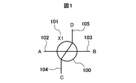
カプラのシンボルとしては、例えば、図1に示すカプラシンボル100がある。
【0044】
同図中、101はカプラシンボル100に付加される部品番号である。カプラシンボル100には、4つの端子102,103,104,105が設けられている。端子102,103は1本の配線で結線されている。また、端子104,105も1本の配線で結線されている。このカプラシンボル100では、前者の配線と後者の配線とが、カプラとして非接触で結合されていることを示す。
【0045】
図2は、図1に示すカプラシンボル100がレイアウト図エディタ1922でレイアウトされた例である。
【0046】
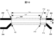
レイアウトされたカプラ200は、配線間隔Dcで、長さLcの2本の平行配線である。カプラを構成している2本の配線には、それぞれの配線の始点および終点を示す情報を持つ。この情報は、ポインタP1、P2、P3、P4である。このポインタは、図1の端子102,103,104,105にそれぞれ対応する。ポインタ102,103,104,105からは、それぞれ配線202,203,204,205が引き出されている。同図では示していないが、配線202,203,204,205は、別の部品又は回路に接続されている。
【0047】
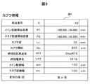
図3は、カプラ情報(カプラ属性情報)301の内容を示している。このカプラ情報301とは、回路図設計支援装置1900及びレイアウト図設計支援装置1920のカプラ・層情報記憶部1906,1927に記憶される情報であって、レイアウト図エディタ1922がカプラシンボルからカプラレイアウト図を作成する際やカプラの動作をシミュレートする際等に使用する情報である。このカプラ情報301は、入力装置1912,1932から回路図エディタ1902又はレイアウト図エディタ1922を介して、カプラ・層情報記憶部1906,1927に登録することができる。また、このカプラ情報301は、入力装置1912,1932から回路図エディタ1902又はレイアウト図エディタ1922に指示を与えることにより、表示装置1911,1931で表示することができる。
【0048】
カプラ情報301には、部品番号X、メイン配線開始座標P1、スタブ配線開始座標P2、カプラ長Lc、カプラ間隔Dc、メイン配線幅wm、スタブ配線幅ws、終端抵抗部品名RTT、終端電源名VTT、カプラの変形を認めるか否か等の項目が含まれている。このカプラ情報301は、レイアウト上のカプラ1つに付き、1つ存在する。
【0049】
カプラ情報301の部品番号Xは、図1のカプラシンボル100の部品番号101と対応している。この部品番号により、回路図エディタ1902とレイアウト図エディタ1922は、カプラを一つの部品として認識すると共に、同一部品番号のカプラは同一部品であると認識する。このため、回路図とレイアウト図との対応関係が極めて明確になり、ユーザーの設計工数を削減することができる。
【0050】
カプラ情報301の開始座標P1,P2は、レイアウト図エディタ1922の動作時に、ユーザーがカプラ200を構成するメイン配線またはスタブ配線をレイアウト図画面上に配置することで、自動的に設定される。また、逆に、レイアウト図エディタ1922の動作時に、ユーザが開始座標P1,P2を設定すると共に、カプラ長Lcとカプラ間隔Dcも設定すると、これらのカプラ情報301を基に、カプラ200を構成するメイン配線またはスタブ配線が自動的に配置される。このように、カプラを構成するメイン配線とスタブ配線を、カプラ長Lcおよびカプラ間隔Dcを用いて関連付けることで、座標設定の手間等、配線レイアウト作業の工数を削減することが可能となる。
【0051】
図4は、他のカプラシンボルの例である。同図のカプラシンボル400と図1のカプラシンボル100との相違点は、図1における端子105が省略されている点である。これは、端子105には、基本的に決まって終端抵抗が接続されるため、シンボルとして端子105が省略されていても、実害がないからである。
【0052】
図5は、さらに他のカプラシンボルの例である。同図のカプラシンボルは、図1のカプラシンボル100の端子105に終端抵抗501を接続し、さらにこの終端抵抗501に終端電源VTTを接続したものである。すなわち、同図のカプラシンボルは、図1におけるカプラシンボル100で省略していた終点抵抗及び終端電源を追加したものである。なお、図3における終端抵抗名及び終端電源名は、それぞれ、以上の終端抵抗501の名称、終端電源VTTの名称である。このように、カプラシンボルに終端抵抗名及び終端電源名を付した場合には、カプラ情報301として、終端抵抗部品名RTTと終端電源名VTTの項目を省略することができる。逆に、図1や図4のカプラシンボル100,400のように、シンボル中に終端抵抗及び終端電源を省略した場合には、図3に示すように、カプラ情報301として、これらの情報が必要になる。
【0053】
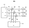
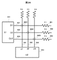
図6は、回路図エディタ1902で作成された回路図の例である。同図に示す回路図には、機能部品611,612が設けられている。各機能部品611,612は、端子D1,D2,CLKを持つ。端子D1と端子D2はバス配線端子で、端子CLKはクロック配線端子である。機能部品611と機能部品612とは、カプラによって接続されている。この回路図でカプラは、図4のカプラシンボル400で示されている。機能部品611の端子D1には、バス配線621、バス配線631、抵抗651が接続され、機能部品611の端子D2には、バス配線622、バス配線632、抵抗652が接続され、機能部品611の端子CLKには、バス配線623、バス配線633、抵抗653が接続されている。また、機能部品612の端子d1には配線641が接続され、機能部品612の端子d2には配線642が接続され、機能部品612の端子clkには配線643が接続されている。
【0054】
図7は、回路図エディタ1902で作成された他の回路図の例で、回路としては図6の回路図が示す回路と等価である。図7の回路図では、図6の機能部品611,612の端子D1,D2を一つのバス配線端子Dで示し、これに伴い、図6のバス配線621,622、カプラシンボル400,400、バス配線631,632、バス配線641,642を、それぞれ、一つのバス配線721、一つのカプラシンボル700、一つのバス配線731、バス配線741で示している。同図のカプラシンボル700は、以上で述べたように、本来、二つのカプラであるが、二つのカプラの仕様が同じであるため、このカプラシンボル700に対するカプラ情報は、一つである。但し、このカプラ情報には、同仕様のカプラが二つである旨の情報が含まれている。この場合、さらに、二つのカプラの相互間隔の情報もカプラ情報に含めるともよい。
【0055】
図8は、図6又は図7の回路図を元にレイアウト図エディタ1922で作成したカプラ回りのレイアウト図の例である。
【0056】
このレイアウト図では、図6のカプラシンボル400で示す三つのカプラX1,X2,X3を、上から順に配置している。端子801,811は、それぞれ、図6の機能部品611,612の端子D1,d1に対応し、端子821,831は、それぞれ、図6の機能部品611,612の端子D2,d2に対応し、端子841,851は、それぞれ、図6の機能部品611,612の端子CLK,clkに対応する。
【0057】
レイアウト図エディタ1922の動作中、ユーザがカプラX1のメイン配線開始座標P1を与えると、機能部品611の端子D1を示す端子801とカプラ800との間隔Lm1が決まるため、端子801の座標が既に定まっていれば、端子801とカプラ800と間にバス配線802が配置される。同様に、ユーザがカプラX1のスタブ配線開始座標P2を与えると、機能部品612の端子d1を示す端子811とカプラ800との間隔Ls1が決まるため、端子811とカプラ800と間に配線812が配置される。
【0058】
バス配線は、対応する他のバス配線と同じ長さにする必要がある。このため、レイアウト図エディタ1922は、機能部品611の各端子801,821,841から対応カプラまでの間隔Lm1,Lm2,Lm3は相互に同じで、機能部品612の各端子811,831,851から対応カプラまでの間隔Ls1,Ls2,Ls3も相互に同じであるとして取り扱う。この結果、レイアウト図エディタ1922は、ユーザがカプラX1の開始座標P1,P2を与えた時点で、機能部品611,612の端子D2,d2を示す端子821,831との関係において、カプラX2の開始座標P21,P22を定め、さらに機能部品611,612の端子CLK,clkを示す端子841,851との関係において、カプラX3の開始座標P31,P32を定める。従って、ユーザがカプラX1のメイン配線開始座標P1,P2を与えた後、各バス配線802,812,822,832,842,852の配置を指示するだけで、別途、配線終端座標等を与えなくても、各バス配線は自動的に配置される。
【0059】
また、各カプラの終端側の各バス配線803も、カプラ800から終端抵抗等の端子804までの間隔を相互に等しくする必要があるので、レイアウト図エディタ1922は、以上のバス配線と同様に、配置する。
【0060】
従って、本実施形態では、バス配線を構成する各配線長さを簡単に揃えることができる。これにより、機能部品間のスキューを抑えることができ、実際のプリント配線基板の高速化と、設計工数の削減の両立を図ることができる。
【0061】
ところで、配線レイアウト上、他の部品との関係等で、各バス配線の長さを正確に同じにすることは困難なことが度々ある。そのため、レイアウト図エディタ1922には、各バス配線の長さに許容範囲が設けられており、例えば、配線長Lm1の20パーセント以内という配線ルールが設けられている。そして、レイアウト図エディタ1922は、あるバス配線802に対して、他のバス配線822の長さを同じにできないときには、この許容範囲内で、他のバス配線822の長さを短く又は長くする。
【0062】
次に、カプラ200のカプラ長を変更する手順について説明する。
【0063】
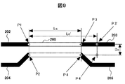
まず、図9に基づいて、カプラ長Lc’をLcに短くする場合の手順について説明する。
【0064】
カプラ長を短くする場合、機能部品側の座標P1,P2の座標は固定として、座標P3,P4をカプラ長に合わせて移動する。これは、座標P1,P2の位置は、機能部品とカプラとの間の配線距離に影響し、P1,P2側を移動すると、機能部品間の信号伝搬時間が変わってしまうためである。
【0065】
座標P3は、配線203の延長線上を移動する。また、座標P4は、カプラ間隔Dcを確保するため、線分P1−P3に対して線分P2−P4が平行になるように移動する。P3,P4の移動後、配線203の開始座標をP3’からP3に移動して、新たに配線203を配置し、配線205の開始座標をP4’からP4に移動して、新たに配線205を配置する。
【0066】
次に、図10に基づいて、カプラ長Lc’をLcに長くする場合の手順について説明する。
【0067】
カプラ長Lc’を長くする場合、前述の短くする場合と同様に、機能部品側の座標P1,P2の座標を固定して、座標P3,P4をカプラ長Lcに合わせて移動する。
【0068】
座標P3は、配線203上を移動する。また、座標P4は、カプラ間隔Dcを確保するため、線分P1−P3に対して線分P2−P4が平行になるように移動する。P3,P4の移動後、配線203の開始座標をP3’からP3に移動して、新たに配線203を配置し、配線205の開始座標をP4’からP4に移動して、新たに配線205を配置する。
【0069】
次に、カプラ長変更時のレイアウト図エディタ1922の動作について、図11のフローチャートに従って説明する。
【0070】
レイアウト図エディタ1922は、変更後カプラ長Lcを受け付けると、この変更後カプラ長Lcをカプラ・層情報記憶部1927に仮登録すると共に、現状のレイアウト図に示されているカプラ長Lc’を調べる(ステップ1101)。現状のカプラ長Lc’を調べる際には、対象カプラの開始座標P1と終端座標P2を調べるか、又はカプラ・層情報記憶部1927のカプラ情報301として既に登録されているカプラ長Lc’を抽出する。
【0071】
続いて、変更後カプラ長Lc’は現状のカプラ長Lcよりも長いか否かを判定し(ステップ1102)、変更後カプラ長Lc’が現状のカプラ長Lcよりも長いと判定した際には、伸ばすスタブ配線上に別の配線等が存在するか否かを判断する(ステップ1103)。伸ばすスタブ配線上に別の配線等が存在しないと判断した場合には、前述したように、メイン配線の開始座標P1を基準に、メイン配線の終端座標P3をメイン配線に沿って(Lc−Lc’)だけ移動し、続いて、メイン配線の終端座標P3を基準に、スタブ配線の終端座標P4を移動して、スタブ配線を配線し直す(ステップ1104)。その後、仮登録されていた変更後カプラ長Lcをカプラ・層情報記憶部1927に本登録する。また、ステップ1103で、伸ばすスタブ配線上に別の配線等が存在すると判断した場合には、配置不可の警告を表示装置1933に表示させる(ステップ1105)。その後、カプラ・層情報記憶部1927に仮登録されていた変更後カプラ長Lcを消去する。
【0072】
ステップ1102で、変更後カプラ長Lc’は現状のカプラ長Lcよりも長くないと判定した場合には、変更後カプラ長Lc’は現状のカプラ長Lcよりも短いか否かを判定する(ステップ1106)。変更後カプラ長Lc’は現状のカプラ長Lcよりも短くないと判定した場合には、つまり、変更後カプラ長Lc’は現状のカプラ長Lcと等しいと判定した場合には、そのまま、このカプラ長変更処理ルーチンを終了する。また、変更後カプラ長Lc’が現状のカプラ長Lcよりも短いと判定した場合には、縮めるスタブ配線上に別の配線等が存在するか否かを判断する(ステップ1107)。縮めるスタブ配線上に別の配線等が存在しないと判断した場合には、前述したように、メイン配線の開始座標P1を基準に、メイン配線の終端座標P3をメイン配線に沿って(Lc’−Lc)だけ移動し、続いて、メイン配線の終端座標P3を基準に、スタブ配線の終端座標P4を移動して、スタブ配線を配線し直す(ステップ1108)。また、ステップ1107で、縮めるスタブ配線上に別の配線等が存在すると判断した場合には、配置不可の警告を表示装置1933に表示させる(ステップ1105)。
【0073】
以上のように、カプラ長変更の際には、変更後のカプラ長を与えるだけで、変更後カプラ長で、カプラを構成するメイン配線及びスタブ配線が配置されるので、配線レイアウト修正の作業工数を減らすことができる。
【0074】
次に、カプラ長の求め方について説明する。
【0075】
カプラ長を求めるためには、カプラ・層情報記憶部1906,1927に記憶されているカプラ情報301(図3)のうちのカプラ間隔Dc、メイン配線幅wm、スタブ配線幅wsの他に、図12に示すように、電源層1203,1204の厚さd1,d5、絶縁層1205,1206の厚さd2,d4、メイン配線1201及びスタブ配線1202の層d3も必要である。そのため、これらの値は、カプラ情報301と同様に、カプラ・層情報記憶部1906,1927に層構成情報1301(図13)として記憶されている。なお、この層構成情報1301も、カプラ情報301と同様に、入力装置1912,1932から回路図エディタ1902又はレイアウト図エディタ1922を介して、カプラ・層情報記憶部1906,1927に登録することができ、また、入力装置1912,1932から回路図エディタ1902又はレイアウト図エディタ1922に指示を与えることにより、表示装置1911,1931で表示することができる。
【0076】
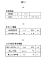
カプラ長の設定にあたっては、さらに、基板材料の情報、ドライバ仕様の情報、カプラの設計条件の情報が必要である。基板材料情報としては、図14(a)に示すように、プリント配線基板に用いる絶縁材の比誘電率εrと、抵抗率σとがある。ドライバ情報としては、図14(b)に示すように、波形遷移時間tr、tfと、信号出力レベルVHとがある。また、カプラ設計条件情報としては、図14(c)に示すように、最小入力信号レベルVswと、最大カプラ長Lcmaxと、最大入力信号幅Twの項目とがある。これらの値も、図19では図示していないが対応する記憶部に登録することになる。
【0077】
次に、図17に示すフローチャートに従って、カプラ長の設定手順について説明する。カプラ長は、カプラをレイアウトする際に必要な情報であるため、少なくともレイアウト前にカプラ長を一度求めておく必要がある。このため、この実施形態では、回路図設計支援装置1900にカプラ長設定部1907が設けられていると共に、レイアウト中にカプラ長を求めることも考慮して、レイアウト図設計支援装置1920にも、同様のカプラ長設定部1928が設けられている。なお、以下では、回路図設定支援装置1900のカプラ長設定部1907の動作について説明する。
【0078】
まず、カプラ長設定部1907は、図14(a)に示す基板材料情報、図3に示すカプラ情報301、及び図13に示す層構成情報1301を基に、カプラの単位長さ当たりの分布定数回路を求める(ステップ1701)。これには、基板断面形状から分布定数回路を求めるためのシミュレータを用いる。この処理で、分布定数回路モデルを得ることができる。
【0079】
次に、検証用変数Lc’に、カプラ情報301に仮設定したカプラ長Lcを設定する(ステップ1702)。これにより、検証の開始ポイントを定義する。
【0080】
次に、簡易回路シミュレータ1903に、ステップ1701で求めた単位長さ当たりの分布定数回路及びステップ1702で設定した検証用変数Lc’の長さを与えて、検証用カプラ長での回路モデルを生成し、この回路モデルで回路シミュレーションを行う(ステップ1703)。ここでは、図14(b)及び図15に示すように、ドライバの出力波形として、波形遷移時間tr,tfが500ps、信号出力レベルVHが1.8Vの用いて、検証用カプラを介してレシーバに入力する波形を調べる。具体的には、図16に示すレシーバの入力波形から信号振幅Vsw’を計測する(ステップ1704)。続いて、この信号振幅Vsw’と、図14(c)に示すカプラ設計条件情報の信号振幅Vswとの大小関係を比較する(ステップ1705)。そして、Vsw’の方が小さくない場合、カプラ長Lcが足りないと判断し、検証用変数Lc’に1mm加算し(ステップ1706)、この加算した値を最大カプラ長Lcmaxと比較する(ステップ1707)。LcmaxよりもLc’が大きい場合は、設計限界と判断し、表示装置1911に「設計限界」の旨を表示させる(ステップ1808)。また、Vsw’がLcw以下であれば、ステップ1703に戻る。
【0081】
ステップ1705の判断で、計測信号振幅Vsw’の方が小さいと判断した場合、この計測信号振幅Vsw’が、カプラ設計条件情報の最小信号振幅Vswの110パーセント以上であれば、逆に信号振幅が大きいと判断し(ステップ1709)、検証用変数Lc’から1mm減算してから(ステップ1710)、ステップ1703に戻る。
【0082】
計測信号振幅Vsw’が設計最小信号振幅Vsw以上であり、且つVswの110パーセント未満であれば、そのカプラ長は設計最適値と判断し、このカプラ長が最適である旨を表示装置1911に表示させる(ステップ1711)。そして、ユーザーに対して、このLc’をカプラ情報301に書き込むかどうかを問い合わせ(ステップ1712)、ユーザーが書き込みを希望する場合は、Lc’の値をカプラ情報301に書き込む(ステップ1713)。その後、レイアウト図作成中であれば、前述の図11に示したカプラ長変更の処理を行う(ステップ1714)。
【0083】
以上のように、ユーザーが、レシーバでの信号受信に必要な信号振幅Vswを与えることで、最適なカプラ長Lcを自動的に計算することができ、設計効率の向上と、クロストークを用いたバスシステムの高性能化を図ることが可能である。
【0084】
次に、レイアウト図設計支援装置1920の配線ルール情報記憶部1925に記憶されている配線ルール情報について、図18を用いて説明する。
【0085】
この配線ルール情報1801は、一旦、回路レイアウト図を作成した後、配線ルール違反が在るか否かのチェックに必要な情報である。この配線ルール情報1801では、バイヤ−配線間ds1、バイヤ−バイヤ間ds2、配線−配線間ds3、カプラ−カプラ間ds4、カプラ−配線間ds5、カプラ−バイア間ds6の最小間隔を定めている。ここでは、カプラを従来技術のように二つの単なる配線として扱わず、カプラとしての一部品として扱っているため、従来の配線ルール情報にはないカプラ−カプラ間ds4、カプラ−配線間ds5、カプラ−バイア間ds6が別途定められている。
【0086】
このように、本実施形態では、カプラを一部品として扱っているため、カプラを構成する二つの配線間隔をチェックすることがなくなる上に、カプラを構成する二つの配線それぞれに対して他の配線等との間隔チェックを行う必要もなくなるため、作業効率を高めることができる。また、カプラは、二つの配線で構成されるものの、本来的に、二つの配線により一つの機能を実現するものである上に、カプラとして二つの配線が扱う信号振幅が微弱であるため、カプラを一つの部品として扱って、このカプラと他の配線等との間隔を規定した方が、カプラ機能をより確実に確保することができる。
【0087】
なお、以上のおいて、バイヤとは、層間配線のことで、配線とは、一層内での配線のことである。
【0088】
次に、図21に示すフローチャートに従って、本実施形態の設計支援システムの動作について説明する。
【0089】
まず、回路図設計支援装置1900の回路図エディタ1902がユーザからの指示を受け付けて、回路図作成・編集を行う(ステップ2101)。このステップ2101では、部品シンボル記憶部1904に記憶されている各種シンボルを配置し、配置した複数のシンボル相互間を結線し、作成した回路図を回路図情報として、回路図情報記憶部1905に記憶する。なお、以上のステップ2101の詳細に関しては、図22を用いて後述する。
【0090】
次に、回路図設計支援装置1900の簡易シミュレータ1903が、ユーザからの指示を受け付けて、ステップ2101で作成した回路図が示す回路の動作をシミュレートし(ステップ2102)、回路動作を確認する(ステップ2103)。このシミュレートでは、大まかな回路動作シミュレートのほかに、製造時に使用する材料や配線レイアウト後の配線長等の大まかな見積もりも行う。さらに、図17を用いた前述したカプラ長の設定のためのシミュレートも行う。
【0091】
以上のシミュレートの結果(ステップ2103)、回路図が不適切なものであれば、簡易シミュレータ1903は、不適切な部分の内容を表示装置1911に表示させて、回路図エディタ1902による回路図作成・編集(ステップ2101)を促す。また、回路図が適切なものであれば、レイアウト図設計支援装置1920のレイアウト図エディタ1922が、ユーザからの指示を受け付けて、配線レイアウト作成・編集を行う(ステップ2104)。このレイアウト図の作成に移行する段階で、回路図設計支援装置1900の回路図情報記憶部1905に記憶されている回路図情報、カプラ・層情報記憶部1906に記憶されているカプラ情報及び層構成情報は、通信部1908により、レイアウト図設計支援装置1920へ送られる。回路図設計支援装置1900からの情報は、レイアウト図設計支援装置1920の通信部1908で受信されて、回路図情報記憶部1925やカプラ・層情報記憶部1906に記憶される。
【0092】
ステップ2104では、まず、レイアウト図エディタ1922のレイアウト部(部品配置手段)1935が、回路図情報が示す部品や配線等をユーザからの指示に従って配置する。なお、ここで配置する部品および配線の情報は、前述のステップ2101で作成した回路図の情報と1対1で対応する。このレイアウト部1935でレイアウト図が作成されると、このレイアウト図の情報がレイアウト図情報として、レイアウト図情報記憶部1925に記憶される。その後、このレイアウト図の配線を配線チェック部1936がチェックし、エラー箇所があれば、その内容を表示し、レイアウト部1935によるレイアウト図の再編集を促す。なお、以上のステップ2104におけるレイアウト部1935の詳細動作、及び配線チェック部1936の詳細動作に関しては、それぞれ、図23及び図24、図25を用いて後述する。
【0093】
次に、レイアウト図設計支援装置1920の詳細シミュレータ1923が、ユーザからの指示を受け付けて、ステップ2104で作成したレイアウト図が示す回路の動作をシミュレートし(ステップ2105)、回路動作を確認する(ステップ2106)。このシミュレート(ステップ2105)では、ステップ2102の簡易シミュレートよりも、更に詳細なシミュレートを行う。具体的には、ここでは、配線の遅延時間や、隣接配線間のクロストークノイズ等を、回路シミュレーションによって検証する。
【0094】
以上の詳細シミュレートの結果(ステップ2105)、レイアウト図が不適切なものでなければ、詳細シミュレータ1923は、不適切な部分の内容を表示装置1931に表示させて、レイアウト図エディタ1922によるレイアウト図作成・編集(ステップ2104)を促す。例えば、詳細シミュレートの結果、カプラ長が原因で、適切な動作がなされていないとなった場合には、ステップ2104に戻って、図11に示すカプラ長の変更処理を行う。また、レイアウト図が適切なものであれば、回路製造データ作成装置1940の製造データエディタ1942が、レイアウト図設計支援装置1920からのレイアウト図情報を回路製造データに変換し、これを回路製造データ記憶部1943に登録する(ステップ2107)。なお、この回路製造データは、カバーデータと呼ばれることもある。
【0095】
以上で、本実施形態の設計支援システムによる処理は終了する。
【0096】
その後、回路製造データ作成装置1940の回路製造データ記憶部1943に記憶されている回路製造データに基づいて、プリント配線基板の試作製造を行う。(ステップ2108)。このステップ2108の作業では、プリント配線基板上に機能部品を実装する作業も含む場合もある。
【0097】
試作基板の製造後(ステップ2108)、この試作基板を実際に動作させて、動作状態を検証、評価する(ステップ2109)。この結果が不合格であれば、ステップ2104の配線レイアウト作成処理、又はステップ2101の回路図作成処理まで戻る。合格であれば、実際に、プリント配線基板の量産を行う(ステップ2111)。
【0098】
次に、図22に示すフローチャートに従って、以上で説明した回路図作成・編集処理(ステップ2101)の詳細処理について説明する。
【0099】
回路図設計支援装置1900の回路図エディタ1902が起動すると、まず、部品シンボル記憶部1904から部品シンボルを読み込む(ステップ2201)。続いて、ユーザからの指示が回路図情報の変更である場合には、回路図情報記憶部1905に記憶されている回路図情報を読み出して、この回路図の画面を表示装置1911に表示させ、ユーザからの指示が新規作成の場合には、回路図新規作成画面を表示装置1911に表示させる(ステップ2202)。
【0100】
次に、入力装置1912がシンボル配置指示又は配線配置指示を受け付ける(ステップ2203又は2208)。ステップ2203でシンボル配置指示を受け付けた場合には、各種部品シンボルを表示装置1911に表示させて、配置するシンボルの選択を受け付ける(ステップ2204)。回路図エディタ1902は、ユーザが選択したシンボルはカプラであるか否かを判断し(ステップ2205)、カプラであれば、このカプラのシンボルをユーザからの指示に従って所望の位置に配置する(ステップ2206)。ユーザは、基本的には、この段階で、カプラ・層情報記憶部1906にカプラ情報及び層構成情報を登録することが好ましい。この際、カプラ情報の一つであるカプラ長Lcに関しては、ここで、カプラ長設定部1907を動作させて、図17を用いて前述したように、カプラ長を設定してもよいが、カプラを構成する配線を実際に配置する直前に設定してもよい。また、ユーザが選択したシンボルがカプラ以外であれば、そのシンボルをユーザからの指示に従って所望の位置に配置する(ステップ2206)。
【0101】
また、ステップ2208で配線配置指示を受け付けた場合には、配線の始点位置を受け付ける(ステップ2209)。この場合、ユーザは、例えば、部品シンボル中の端子の表示画面上で指定してもよいし、配線始点位置の座標を入力してもよい。続いて、始点位置の受付と同様に、配線の終端位置を受け付ける(ステップ2210)。始点位置及び終点位置を受け付けると、始点から終点までの間に配線を引く(ステップ2211)。以上のようにして、仮に、カプラ回りの回路図を作成した場合には、この段階で、表示装置1911には、図26のような画面が表示される。なお、この画面に表示されている回路図は、図6に示した回路図と同じものである。
【0102】
ステップ2208又はステップ2211の後、回路図の保存指示及び回路図作成・編集の終了指示を受け付けなければ(ステップ2212,2214)、ステップ2203に戻る。また、ステップ2212で回路図の保存指示を受け付けると、この回路図の情報を回路図情報記憶部1905に保存する(ステップ2213)。また、ステップ2214で回路図作成・編集の終了指示を受けると、以上の処理が終了する。
【0103】
以上のように、本実施形態では、回路図において、カプラは一部品としてシンボル表示されるので、回路図中のどの部位がカプラを構成するかを識別できるので、ユーザは、レイアウト図との対応関係を容易に認識することができる。また、レイアウト図を作成するレイアウト図設計支援装置1920にとっても、どの部位をカップとして配置すべきかを認識することができる。
【0104】
次に、図23及び図24に示すフローチャートに従って、先に説明した配線レイアウト作成・編集処理(ステップ2104)の詳細処理について説明する。
【0105】
レイアウト図設計支援装置1920のレイアウト図エディタ1922のが起動すると、まず、エディタ1922のレイアウト部1935が配線ルール情報記憶部1926から配線ルール情報を読み込み、カプラ・層情報記憶部1927からカプラ情報及び層構成情報を読み込む(ステップ2301)。さらに、回路図情報記憶部1924に記憶されている回路図情報を読み込む(ステップ2302)。なお、配線ルール情報の読み込みは、後述する配線ルールチェックを実行する際に読み込むようにしてもよい。続いて、ユーザからの指示がレイアウト図情報の変更である場合には、レイアウト図情報記憶部1925に記憶されているレイアウト図情報を読み出して、このレイアウト図の画面を表示装置1931に表示させ、ユーザからの指示が新規作成の場合には、レイアウト図新規作成画面を表示装置1931に表示させる(ステップ2303)。
【0106】
次に、入力装置1932がシンボル配置指示又は配線配置指示を受け付ける(ステップ2304又は2311)。ステップ2304でシンボル配置指示を受け付けた場合には、回路図中のどのシンボルをレイアウト図中に配置するかを受け付ける(ステップ2305)。レイアウト部1935は、ユーザが選択したシンボルはカプラであるか否かを判断し(ステップ2306)、カプラであれば、このカプラシンボルの部品番号を参照して、カプラ・層情報記憶部1927から対応するカプラ情報301を読み出して、カプラ長Lc及びカプラ間隔Dcを取得する(ステップ2307)。続いて、カプラの開始座標P1及びカプラの伸張方向を受け付けると(ステップ2308)、図8等を用いて前述したように、メイン配線及びサブ配線を配置する(ステップ2309)。なお、メイン配線及びサブ配線の際に、これらの配線が他の配線又は他の機能部品と重なる場合には、基本的に、これらを迂回するように配置される。但し、図3に示す回路情報301で、「変形の良・否」が「否」となっている場合には、他の配線又は他の機能部品を移動させても良いか否かを表示し、移動許可を受けた場合には、他の配線又は他の機能部品を移動させて、メイン配線及びサブ配線の直線性を確保する。
【0107】
ステップ2306で、ユーザが選択したシンボルがカプラ以外である場合には、そのシンボルに配置に必要な座標等の情報を受け付けて、この情報に従ってシンボルを配置する(ステップ2310)。なお、ここで配置する部品シンボルは、回路図で配置した部品シンボルと同じものでもよいが、好ましくは実際の部品寸法に対応したあるものが好ましく、例えば、抵抗であれば、実際の抵抗の長さに対応したものであることが好ましい。この場合、レイアウト図設計支援装置1920も、このようなシンボルが記憶されている部品シンボル記憶部を有する必要があることは言うまでもない。
【0108】
また、ステップ2311で配線配置指示を受け付けた場合には、配線の始点位置を受け付ける(ステップ2312)。この場合、ユーザは、例えば、部品シンボル中の端子の表示画面上で指定してもよいし、配線始点位置の座標を入力してもよい。続いて、始点位置の受付と同様に、配線の終端位置を受け付ける(ステップ2313)。始点位置及び終点位置を受け付けると、始点から終点までの間に配線を引く(ステップ2314)。以上のようにして、仮に、カプラ回りのレイアウト図を作成した場合には、この段階で、表示装置1931には、図27のような画面が表示される。なお、この画面に表示されているレイアウト図は、図8に示したレイアウト図と同じものである。
【0109】
配線を引いた後、配線ルールチェック実行を受け付けると(ステップ2315、以下、ステップ2321まで図24に示す)、レイアウト図エディタ1922の配線チェック部1936が起動し、ステップ2301で読み込んだ配線ルール情報を用いて、配線間隔をチェックする(ステップ2316)。
【0110】
ステップ2315又はステップ2316の後、レイアウト図の保存指示及びレイアウト図作成・編集の終了指示を受け付けなければ(ステップ2317,2319)、図23のステップ2304に戻る。また、ステップ2317でレイアウト図の保存指示を受け付けると、このレイアウト図の情報をレイアウト図情報記憶部1925に保存する(ステップ2318)。また、ステップ2319でレイアウト図作成・編集の終了指示を受けると、以上の処理が終了する。
【0111】
次に、図24のステップ2316における配線ルールチェックの詳細処理について、図25に示すフローチャートに従って説明する。
【0112】
この配線ルールチェックでは、先ず配線チェック部1936の対象抽出部1937が起動して、対象ネットを受け付けると共に、この対象ネットの近傍にある対象相手ネットを抽出して、これらのネットを構成要素の分解する(ステップ2501)。この対象ネットの近傍にある対象相手ネットの抽出にあたっては、対象ネットに対して予め定められた範囲内に入っている全てのネットを抽出する。ここで、ネットとは、ある部品等の端子から他の部品等の端子までの一連の配線、又は、この一連の配線及びこれに接続した機能部品を含むものである。また、ネットを構成要素に分解するとは、配線と機能部品とを分解すると共に、一連の配線を屈曲点や分岐点等で分解し、配線を直線成分又は一定の曲率の曲線成分のみにすることである。
【0113】
ところで、本実施形態では、カプラを二つの配線としてではなく、一部品として取り扱っているため、対象ネット又は対象相手ネット内にカプラが存在していても、このカプラを二つの配線に分解せず、一つのカプラとして配線ルールチェックが行われる。このため、カプラを構成する二つの配線の相互間隔は、配線ルールチェック対象外になる。なお、対象ネット又は対象相手ネット内にカプラが存在するか否かは、これらのネット内に、カプラに付した部品番号を示すものが存在するか否かで判断する。
【0114】
対象抽出部1937は、対象ネットを構成する要素群及び対象相手ネットを構成する要素群から、それぞれ一つずつ抽出して、これらの要素を配線チェック部1936の配線チェッカー1938に渡す(ステップ2502)。
【0115】
配線チェッカー1938は、まず、二つの要素間の最短距離spを調べる(ステップ2503)。続いて、二つの要素はどちらもVIAか否かを判断し(ステップ2504)、二つの要素ともVIAである場合には、図18に示す配線ルール情報1801で規定するVIA−VIA間の最小間隔ds2と、ステップ2503で調べたspとの大小関係を比較する(ステップ2505)。この比較の結果、sp<sp2の場合には、この二つの要素が配線ルール違反である旨を表示装置1931に表示させる(ステップ2514)。
【0116】
以下、二つの要素のうち一方がカプラで他方が配線である場合には、配線ルール情報1801で規定するカプラ−配線間の最小間隔ds5を用いて配線間隔チェックを行い(ステップ2507,2508,2513)、一方がカプラで他方がVIAである場合には、配線ルール情報1801で規定するカプラ−VIA間の最小間隔ds6を用いて配線間隔チェックを行い(ステップ2509,2513)、両方がカプラである場合には、配線ルール情報で規定するカプラ−カプラ間の最小間隔ds4を用いて配線間隔チェックを行い(ステップ2510,2513)、両方とも配線である場合には、配線ルール情報1801で規定する配線−配線間の最小間隔ds3を用いて配線間隔チェックを行い(ステップ2511,2514)、一方が配線で他方がVIAである場合には、配線ルール情報1801で規定する配線−VIA間の最小間隔ds1を用いて配線間隔チェックを行う(ステップ2512,2514)。
【0117】
二つの要素に関して、配線間隔チェックが終了すると、全ての要素に関して、配線間隔チェックが終了したか否かを判断し(ステップ2515)、全ての要素に関して配線間隔チェックが終了していなければ、ステップ2502に戻る。また、全ての要素に関して配線間隔チェックが終了していれば、対象ネット及び対象相手ネットに関する配線ルールチェックは終了する。なお、終了段階で、配線ルール違反が無ければ、対象ネット及び対象相手ネット内には、配線ルール違反がない旨を表示装置1931に表示させる。
【0118】
次に、以上で説明した設計支援システムで設計し、この設計に基づいて製造したプリント配線基板について説明する。
【0119】
まず、製造するプリント配線基板の回路について、図28を用いて説明する。
【0120】
この回路は、ドライバ2801と、このドライバ2801から伸びるドライバ信号線2802と、ドライバ信号線2802の端部に接続されているドライバ終端抵抗2803と、4つのレシーバ2810,2820,2830,2840と、各レシーバから伸びるレシーバ信号線と、各レシーバ信号線に接続されているレシーバ終端抵抗2816,2826,2836,2846と、を有している。ドライバ信号線2802に対して、4つのレシーバ信号線の一部分が一定の間隔で平行に配置されている。各レシーバ信号線の一部分と、これらの部分に平行なドライバ信号の各部分は、カプラ2813,2823,2833,2843を形成している。つまり、各レシーバ信号線の一部分は、各カプラのスタブ配線2812,2822,2832,2842を形成し、ドラバ信号の複数の部分は、各カプラのメイン配線2811,2821,2831,2841を形成している。
【0121】
以上のような回路を従来技術で設計し、これに基づいてプリント配線基板を製造すると、図29に示すようなプリント配線基板が製造される。
【0122】
このプリント配線基板2900は、基板本体の上面に、ドライバ2801が設けられていると共に、第一のレシーバ2810と第四のレシーバ2840と第二のレシーバ2820と第三のレシーバ2830とがコネクタ2814,2844,2824,2834を介して互いに等間隔で設けられ、さらに、ドライバ終端抵抗2803と第一のレシーバ終端抵抗2816と第二のレシーバ終端抵抗2826とが互いに等間隔で設けられている。また、基板本体の裏面には、第三のレシーバ終端抵抗2836と第四のレシーバ終端抵抗2846とが設けられている。この第三のレシーバ終端抵抗2836と第四のレシーバ終端抵抗2846との間隔は、第一のレシーバ終端抵抗2816と第二のレシーバ終端抵抗2826との間隔と同じである。
【0123】
基板本体の上面に設けられている4つのレシーバコネクタ2814,2844,2824,2834からは、基板本体の裏面まで伸びているスルーホール2815,2845,2825,2835が形成されている。レシーバ信号線は、このスルーホールの一部と、スルーホールの途中から基板本体の上面と平行な面内で伸びている部分と、その端部から基板本体の上面又は裏面に設けられている終端抵抗まで伸びている部分で形成されている。
【0124】
ドライバ信号線2802は、ドライバ2801から最も遠い位置に配置されている第三のレシーバ2830よりも更に遠い位置に形成されているスルーボール2805が折り返し部分を成し、このスルーホール2805から、ドライバ2801と第一のレシーバ2810との間に配置されているドライバ終端抵抗2803まで伸びている。
【0125】
各カプラ2813,2823,2833,2843は、スルーホール2845,2835,2825,2815を回避するため、いずれも迂回している。具体的には、図30に示すように、第一のカプラ2813のメイン配線2811は、第一のスルーボール2815を避けるために、第一のスルーホール2815から水平方向に一定距離離れている。この第一のスルーホール2815から伸びる第一のカプラ2813のスタブ配線2812は、第四のスルーホール2845を避けるために水平方向に迂回している。このため、メイン配線2811も、スタブ配線2812との平行性を維持するために、同様に迂回している。
【0126】
このように、カプラを迂回させると、カプラと屈曲部分で信号の反射現象が生じるため、クロストーク信号が歪んで所望のクロストーク信号を得ることが極めて難しく、データ転送速度を高めることができない。仮に、所望のクロストーク信号を得ようとするならば、このカプラを屈曲点毎に分割して、分割部分毎にシミュレートする必要があるため、カプラの設計に多くの工数がかかってしまう。
【0127】
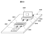
これに対して、本実施形態では、図3に示すカプラ情報301の「変形の良・否」を「否」に設定すると、図23のステップ2309において、前述したように、カプラが他の配線又は他の機能部品と重なる場合には、これらを移動して、カプラの直線性が確保されるので、図31及び図33に示すようなプリント配線基板3100を得ることができる。
【0128】
このプリント配線基板3100も、従来技術によるプリント配線基板2900と同様に、基板本体の上面に、ドライバ2801、第一から第4のレシーバ2810,2820,2830,2840、ドライバ終端抵抗2803、第一のレシーバ終端抵抗2816、第二のレシーバ抵抗2826が設けられ、基板本体の裏面に、第三のレシーバ終端抵抗2836、第四のレシーバ終端抵抗2846が設けられている。しかしながら、このプリント配線基板3100では、レイアウト図設計段階で、カプラの直線性を維持するためにスルーホールを移動した結果、レシーバの配列順が変わった上に、レシーバ相互間隔及び終端抵抗相互間隔も等間隔ではなくなっている。
【0129】
具体的には、従来のプリント配線基板2900では、各レシーバは、ドライバ側から、第一のレシーバ2810、第四のレシーバ2840、第二のレシーバ2820、第三のレシーバ2830の順で並んでいるが、本実施形態のプリント配線基板3100では、ドライバ側から、第四のレシーバ2840、第一のレシーバ2810、第三のレシーバ2830、第二のレシーバ2820の順で並んでいる。また、従来のプリント配線基板2900では、隣り合う各レシーバ相互の間隔が前述したように等間隔であるが、本実施形態のプリント配線基板3100では、第四のレシーバ2840と第一のレシーバ2810との間隔と、第三のレシーバ2830と第二のレシーバ2820との間隔とは同じであるものの、第四のレシーバ2840と第一のレシーバ2810との間隔と、第一のレシーバ2810と第三のレシーバ2830との間隔とは同じではない。
【0130】
本実施形態では、以上のようなレイアウトを行った結果、前述したように、全てのカプラの直線性は確保さている。具体的には、図32に示すように、第一のカプラ2813のメイン配線2811にも、スタブ配線2812にも、スルーホールが邪魔にならないため、第一のカプラ2813を構成するメイン配線2811及びスタブ配線2812は、いずれも直線である。
【0131】
従って、本実施形態では、所望のクロストーク信号を得ることができるカプラを製造することができる。
【0132】
なお、以上では、カプラ情報301の「変形の良・否」を「否」に設定した場合のカプラ構成であるが、さらに、カプラ情報301として、「配線の上下重複の有・無」を追加し、これを「有」に設定できるようにして、図34に示すように、スタブ配線2812とメイン配線2811とを上下方向において重なり合うようにレイアウトしてもよい。この場合、図32において二点破線で示すように、第一のスルーホール2815からのレシーバ信号線を一旦ドライバ信号線側に向けて、ドライバ信号線2802の真下を通るようし、そこにスタブ配線2812を形成し、スタブ配線2812の端部からのレシーバ信号線を再びドライバ信号線2802から離れる方向に向けて、適当な位置から立ち上げて、その上端にレシーバ終端抵抗2816を設けるとよい。
【0133】
以上のようなレイアウトの場合、図34に示すように、基材3401の一方の面と他方の面の対応する位置に、それぞれ、メイン配線2811とスタブ配線2812を接着材3402,3403で貼り付け、この接着剤3402,3403の外側に電源配線層3404,3405を貼り付けると、同一基材3401にメイン配線2811とスタブ配線2812とを設けることになるので、製造バラツキによる配線位置ズレを最小限に抑えることができ、カプラの性能劣化を抑えることができる。また、メイン配線2811とスタブ配線2812とを上下方向に重ねて配置することで、クロストーク電圧を高めやすくなり、結果としてデータ転送速度を高めることができる。
【0134】
【発明の効果】
回路図の設計支援に関する発明によれば、方向性結合器が単なる配線としてではなく、部品シンボルとして回路図に描かれるので、回路図から方向性結合器を形成する配線を簡単に見出せる上に、この回路図とレイアウト図との対応関係を容易に認識することができる。この結果、この回路図に基づくレイアウト図の作成工数を減らすことができる。
【0135】
また、レイアウト図の設計支援に関する発明によれば、方向性結合器を形成する二つの配線は、一つの部品として扱われるため、間隔チェックの際には、この二つの配線の間隔チェックは行われず、一つの部品としての方向性結合器と他の配線との間の間隔チェックが行われるので、間隔チェックが効率的に且つ高精度で行われ、レイアウト図の作成工数を減らすことができる。
【0136】
また、レイアウト図の設計支援で設計された回路基板に係る発明によれば、方向性結合器が直線状に形成されるために、クロストーク信号の歪みを抑えることができ、データ転送速度を高めることができる。
【図面の簡単な説明】
【図1】本発明に係る第1の実施形態としてのカプラシンボルを示す説明図である。
【図2】図1のカプラシンボルをレイアウトしたレイアウト図である。
【図3】本発明に係る一実施形態としてのカプラ情報の構成を示す説明図である。
【図4】本発明に係る第二の実施形態としてのカプラシンボルを示す説明図である。
【図5】本発明に係る第三の実施形態としてのカプラシンボルを示す説明図である。
【図6】本発明に係る第一の実施形態としての回路図である。
【図7】本発明に係る第二の実施形態としての回路図である。
【図8】図6又は図7の回路図をレイアウトしたレイアウト図である。
【図9】本発明に係る一実施形態としてのカプラ長の伸張方法を示す説明図である。
【図10】本発明に係る一実施形態としてのカプラ長の縮小方法を示す説明図である。
【図11】本発明に係る一実施形態としてのカプラ長変更の処理手順を示すフローチャートである。
【図12】本発明に係る一実施形態としての層構成情報を説明するための説明図である。
【図13】本発明に係る一実施形態としての層構成情報の構成を示す説明図である。
【図14】本発明に係る一実施形態としての基板材料情報の構成(a)、ドライバ情報の構成(b)、カプラ設計条件情報の構成(c)を示す説明図である。
【図15】ドライバの出力波形を示す説明図である。
【図16】レシーバの入力波形を示す説明図である。
【図17】本発明に係る一実施形態としてのカプラ長の設定処理手順を示すフローチャートである。
【図18】本発明に係る一実施形態としての配線ルール情報の構成を示す説明図である。
【図19】本発明に係る一実施形態としての設計支援システムの機能ブロック図である。
【図20】本発明に係る一実施形態としての回路図設計支援装置の回路ブロック図である。
【図21】本発明に係る一実施形態としてのプリント配線基板の設計から製造までの手順を示すフローチャートである。
【図22】本発明に係る一実施形態としての回路図エディタの動作を示すフローチャートである。
【図23】本発明に係る一実施形態としてのレイアウト図エディタの動作を示すフローチャート(その1)である。
【図24】本発明に係る一実施形態としてのレイアウト図エディタの動作を示すフローチャート(その2)である。
【図25】本発明に係る一実施形態としての配線チェック部の動作を示すフローチャートである。
【図26】本発明に係る一実施形態としての回路図の表示画面を示す説明図である。
【図27】本発明に係る一実施形態としてのレイアウト図の表示画面を示す説明図である。
【図28】複数のカプラを含む回路の回路図である。
【図29】従来のプリント配線回路基板の構成を示す説明図である。
【図30】図29に示すプリント配線回路基板の要部切欠き斜視図である。
【図31】本発明に係る一実施形態の設計方法で設計したプリント配線回路基板の構成を示す説明図である。
【図32】図31に示すプリント配線回路基板の要部切欠き斜視図である。
【図33】図31に示すプリント配線基板の全体斜視図である。
【図34】図31に示すプリント配線基板を一部変更した配線基板の断面図である。
【図35】カプラの構成を示す説明図である。
【図36】カプラを含む回路の従来の回路図である。
【図37】図36の回路図におけるカプラ回りのレイアウト図である。
【符号の説明】
100,400,700…カプラシンボル、200,800…カプラ、301…カプラ情報、1301…層構成情報、1801…配線ルール情報、1900…回路図設計支援装置、1901…回路図設計支援装置の本体、1902…回路図エディタ、1903…簡易シミュレータ、1904…部品シンボル記憶部、1905、1924…回路図情報記憶部、1906,1927…カプラ・層情報記憶部、1907,1928…カプラ長設定部、1908,1929,1944…通信部、1911,1931,1951…表示装置、1912,1932,1952…入力装置、1922…レイアウト図エディタ、1923…詳細シミュレータ、1926…配線ルール情報記憶部、1935…レイアウト部、1936…配線チェック部、1937…対象抽出部、1938…配線チェッカー、1940…回路製造データ作成装置。[0001]
BACKGROUND OF THE INVENTION
The present invention relates to a design support apparatus for a circuit diagram and a circuit layout diagram of a circuit including a directional coupler using crosstalk, and its design support.program,as well asHow to design a circuitTo the lawRelated.
[0002]
[Prior art]
As a technique for transferring data between a plurality of modules, a bus system used for data transfer in a computer is known. In this bus system, a plurality of modules are connected by a common bus, and data is transferred in a time-sharing manner between the modules using the bus as a data transmission path. Such a bus is generally composed of an address signal wiring, a data signal wiring, a control signal wiring, and the like.
[0003]
In a bus system, as a connection form of a bus and a module, a form in which each module is connected to the bus directly or via a resistor, a form in which each module is connected to the bus in a non-contact manner using crosstalk, and the like are known. ing. A configuration in which the crosstalk is used to connect to the bus in a non-contact manner is described in JP-A-2000-132290 and the like.
[0004]
When using crosstalk, for example, as shown in FIG. 35, a
[0005]
In general, when crosstalk occurs between two normal wires, the crosstalk becomes signal noise. Therefore, in order to avoid the crosstalk, the distance between the two wires is set to a certain distance or more. On the other hand, in the above technique, the interval between two wirings is narrowed to intentionally generate crosstalk, and a signal is passed from one wiring to the other wiring in a non-contact manner.
[0006]
Incidentally, a circuit diagram of a bus system using crosstalk is conventionally drawn as shown in FIG.
[0007]
In this circuit diagram,
[0008]
In the figure, 3601, 3602, and 3603 are formed as couplers, and D1 terminals, D2 terminals, and CLK terminals are indirectly connected to each other. In the figure, the
[0009]
When drawing a circuit layout diagram using the above circuit diagram, in the prior art, out of a large number of wirings drawn in the circuit diagram, two wires forming a coupler are selected again, and the two wirings are selected. A circuit layout diagram as shown in FIG. 37 is created by arranging a part of them so as to be parallel to each other at regular intervals. This figure is a layout diagram of
[0010]
[Problems to be solved by the invention]
However, in the above prior art, in the circuit diagram, since the coupler is only treated as a wiring, that is, not drawn as a coupler, when drawing a circuit layout diagram with reference to this circuit diagram, Of the many wirings shown in the circuit diagram, it is necessary to select two wirings that form the coupler, and it takes time to recognize the correspondence between the circuit diagram and the circuit layout diagram. .
[0011]
In particular, when crosstalk is used in bus wiring, the number of couplers is the product of “bus width” and “number of functional parts”. For example, when the bus width is 64 and the number of functional parts is 9, the number of couplers is 512. It becomes an individual. For this reason, much effort is required to recognize the correspondence between the circuit diagram and the circuit layout diagram.
[0012]
Normally, once the circuit layout diagram is completed, the design support apparatus checks the intervals between the numerous wirings, and if a wiring rule violation is found, the wiring layout is re-performed. In this case, as shown in FIG. 37, if the
[0013]
That is, the conventional technique has a problem that much labor is required to create a layout diagram of a circuit including a coupler.
[0014]
This application pays attention to such problems of the prior art, and can reduce the number of man-hours for designing a layout diagram of a circuit including a coupler, a circuit diagram and layout diagram design support device, a system including this device, and a design support Design support for operating computersprogramAn object of the present invention is to provide an invention relating to a design method.
[0015]
[Means for Solving the Problems]
The first design support apparatus for achieving the object is
A first signal line connected to a driver that outputs a signal and a second signal line connected to a receiver that receives a crosstalk signal based on the signal from the driver are partially arranged in parallel. Regarding a circuit including a directional coupler, in a design support device for a circuit diagram showing a connection between components,
Symbol storage means in which symbols predetermined for each part of various parts including the directional coupler are stored;
Among various symbols stored in the symbol storage means,Which symbol to placeSymbol placement means for receiving the symbol placement position and placing the symbol in the accepted placement position;
Circuit diagram information storage means for storing symbols arranged by the symbol arrangement means, and arrangement positions of the symbols;
Attribute information receiving means for receiving coupler attribute information including at least a parallel signal line length and a signal line interval of the directional coupler;
Attribute information storage means for storing the coupler attribute information received by the attribute information receiving means in association with the symbol of the directional coupler arranged or arranged by the symbol arranging means;
It is characterized by having.
[0016]
Moreover, the second design support apparatus for achieving the above-mentioned object is
A first signal line connected to a driver that outputs a signal and a second signal line connected to a receiver that receives a crosstalk signal based on the signal from the driver are partially arranged in parallel. With respect to a circuit including a directional coupler, in a design support apparatus for a circuit layout diagram showing the arrangement of parts and the arrangement of wiring between parts,
Attribute information receiving means for receiving coupler attribute information including at least a parallel signal line length and a signal line interval of the directional coupler;
Based on at least the coupler attribute information received by the attribute information receiving means, the first signal line portion and the second signal line portion constituting the directional coupler are changed to the directional coupler. Component placement means for placing as
A wiring interval check means for checking an interval between two wirings according to a predetermined rule;
The check target by the wiring interval check means is received, and it is determined whether or not the directional coupler is present in the received check target. If the directional coupler is present, the directional coupler is determined. The first signal line portion and the second signal line portion are excluded from the check target of the wiring interval check means with respect to the mutual interval between the first signal line portion and the second signal line portion constituting the first signal line portion. A check target extraction unit that uses the signal line portion as a check target of the wiring interval check unit as a directional coupler;
A design support apparatus comprising:
[0017]
Here, in the second design support device,
A plurality of parts including the directional coupler are indicated by symbols, and circuit diagram information receiving means for receiving information of a circuit diagram in which connection between the parts is shown is provided, and the part placement means includes the circuit When an arrangement relating to a symbol in the circuit diagram information received by the diagram information receiving means is received, whether or not the symbol is the directional coupler based on the coupler attribute received by the attribute information receiving means When the symbol is determined to be the directional coupler, the first signal line portion and the second signal line portion constituting the directional coupler are arranged. You may do.
[0018]
A design support system for achieving the object is as follows:
The first design support device and the second design support device,
The second design support apparatus receives the circuit diagram created by the first design support apparatus, and creates the layout diagram based on the circuit diagram.
[0019]
Here, the design support system may further include a manufacturing data creation device that creates circuit manufacturing data based on the information of the layout diagram.
[0020]
To achieve the purposeFirstDesign supportprogramIs
A first signal line connected to a driver that outputs a signal and a second signal line connected to a receiver that receives a crosstalk signal based on the signal from the driver are partially arranged in parallel. Design support for causing a computer to perform design support for circuit diagrams showing interconnections between components for circuits including directional couplersprogramIn
In the first storage area of the computer,Of the various parts including the directional coupler, the shape of a symbol predetermined for each partSymbol data is stored in advance,
By the input means of the computer,Stored in the first storage areaingAmong various symbol data,An indication of which symbols to placeAnd the placement position of the symbolSymbol placement acceptance procedure,
The symbol instructed in the symbol placement acceptance procedure, the symbol received in the symbol placement acceptance procedureA symbol placement procedure to be placed at the placement position;
A circuit diagram information storing procedure for storing the symbols arranged in the symbol arranging procedure and the arrangement position of the symbols in a second storage area of the computer;
Attribute information receiving procedure for receiving coupler attribute information including at least a parallel signal line length and a signal line interval of the directional coupler;
Attribute information stored in the third storage area of the computer in association with the symbol of the directional coupler arranged or arranged in the symbol arrangement procedure, and the combiner attribute information received in the attribute information reception procedure Storage procedure;
Is executed by the computer.
[0021]
Second design support for achieving the objectprogramIs
A first signal line connected to a driver that outputs a signal and a second signal line connected to a receiver that receives a crosstalk signal based on the signal from the driver are partially arranged in parallel. Design support for causing a computer to execute design support for a layout diagram showing the layout of components and the layout of interconnections between components for a circuit including a directional couplerprogramIn
By the input means of the computer,Attribute information receiving procedure for receiving coupler attribute information including at least a parallel signal line length and a signal line interval of the directional coupler;
Based on at least the coupler attribute information received in the attribute information reception procedure, the first signal line portion and the second signal line portion constituting the directional coupler are changed to the directional coupler. As part placement procedure to place as
A wiring interval check procedure for checking an interval between two wirings according to a predetermined rule;
By the input means,Accept check target by the wiring interval check procedureThe check target reception procedure,
In the check target reception procedureIt is determined whether or not the directional coupler is present in the received check target. If the directional coupler is present, the portion of the first signal line constituting the directional coupler is determined. The first signal line portion and the second signal line portion are unidirectionally coupled while the mutual interval between the second signal line portions is excluded from the check target in the wiring interval check procedure. A check target extraction procedure to be checked by the wiring interval check means as a device;
Is executed by the computer.
[0022]
Here, the second design supportprogramIn
The attribute information reception procedure receives coupler attribute information including identification information of the directional coupler as the coupler information,
The check target extraction procedure is characterized in that, based on the identification information of the coupler attribute information, it is determined whether or not the directional coupler is present in the check target. Also good.
[0023]
In addition, the second design supportprogramIn
A plurality of parts including the directional coupler are indicated by symbols, and a circuit diagram information receiving procedure for receiving information of a circuit diagram in which connection between parts is shown is executed by the computer,
In the component arrangement procedure, when an arrangement relating to a symbol in the circuit diagram information received in the circuit diagram information reception procedure is received, the symbol is moved in the direction based on the coupler attribute received in the attribute information reception procedure. If it is determined whether the symbol is a directional coupler, the first signal line portion and the second signal line constituting the directional coupler are determined. It may be characterized by arranging parts.
[0024]
In addition, the second design supportprogramIn
As the coupler attribute information received in the attribute information reception procedure, the first signal line part and the second signal line part constituting the directional coupler are both bent in a straight line. When there is information indicating that it should not be included, in the component placement procedure, the first signal line portion and the second signal line portion are disposed in the process of placing the first signal line portion and the second signal line portion. Even if it is necessary to bypass the part of one signal line and the part of the second signal line, the part of the first signal line and the part of the second signal line are not bypassed. The component may be moved to maintain the linearity of the first signal line portion and the second signal line portion.
[0025]
Further, the second design supportprogramIn
As the coupler attribute information received in the attribute information reception procedure, the first signal line portion and the second signal line portion constituting the directional coupler are changed from one surface of the circuit board to the other. If there is information indicating that the first signal line and the second signal line are overlapped in the direction, the component placement procedure includes arranging the first signal line part and the second signal line part to overlap in the direction. FeaturesMay be.
[0026]
A design method for achieving the above object is as follows.
A first signal line connected to a driver that outputs a signal and a second signal line connected to a receiver that receives a crosstalk signal based on the signal from the driver are partially arranged in parallel. In a method for designing a circuit including a directional coupler,
In the first storage area of the computer, symbol data relating to the shape of a symbol predetermined for each part of the various parts including the directional coupler is stored in advance.
A symbol placement accepting step of accepting an instruction as to which of the various symbol data stored in the first storage area is placed by the input means of the computer and receiving the placement position of the symbol;
The symbol instructed in the symbol arrangement receiving step, the symbol received in the position receiving stepA circuit diagram creation step of creating a circuit diagram by arranging at a placement position;
Symbols arranged in the circuit diagram creation step, and arrangement positions of the symbolsIn the second storage area of the computerA circuit diagram information storing step for storing;
By the input means,Coupler attribute information including at least a parallel signal line length and a signal line interval of the directional coupler;An attribute information acceptance process to accept;
Attribute information stored in the third storage area of the computer in association with the symbol of the directional coupler arranged or arranged in the symbol arrangement step and the coupler attribute information received in the attribute information reception step Memory process;
The components placed in the layout diagram are the symbols in the circuit diagram.Is a symbol of the directional coupler,If it is a directional coupler symbol,Stored in the third storage areaA component placement step of placing the first signal line portion and the second signal line portion constituting the directional coupler as the directional coupler based on at least the coupler attribute information;
A wiring interval check process for checking an interval between two wirings according to a predetermined rule;
Accepts checks in the wiring interval check processCheck target acceptance process,
In the check target acceptance processIt is determined whether or not the directional coupler is present in the received check target. If the directional coupler is present, the portion of the first signal line constituting the directional coupler is determined. The first signal line part and the second signal line part are unidirectionally coupled while the mutual interval between the second signal line parts is excluded from the check target in the wiring interval check step. A check target extraction step to be a check target in the wiring interval check step,
The computer executesIt is characterized by this.
[0027]
The second design method for achieving the above object is as follows:
A first signal line connected to a driver that outputs a signal and a second signal line connected to a receiver that receives a crosstalk signal based on the signal from the driver are partially arranged in parallel. In a design method for designing a circuit including a directional coupler using a computer,
Storing information of the directional coupler, which is determined under a condition that the directional coupler generates the crosstalk signal;
In the layout diagram, when an instruction to place the directional coupler is received, the portion of the first signal line and the second signal forming the directional coupler based on the information of the directional coupler A line portion is arranged.
[0028]
Here, the information on the directional coupler includes identification information for identifying the directional coupler, lengths of the first signal line portion and the second signal line portion that form the directional coupler. And a distance between the first signal line portion and the second signal line portion forming the directional coupler. In this case, the interval may be the maximum value of the interval at which the crosstalk signal is generated between the first signal line portion and the second signal line portion. In addition, you may change this space | interval suitably in the range which does not exceed the maximum value.
[0029]
The circuit board designed in the invention related to the above design support is
A driver for outputting a signal, a first signal line connected to the driver, a plurality of receivers for receiving a crosstalk signal based on a signal from the driver, and a second connected to the plurality of receivers, respectively. Signal lines and a substrate body provided with these signal lines,
In a circuit board in which a plurality of stub wirings that are parts of the second signal lines and a main wiring that is a part of the first signal lines are arranged in parallel to each other to form a plurality of directional couplers ,
The plurality of directional couplers are characterized in that the main wiring and the stub wiring forming the directional coupler are both straight and parallel to each other.
[0030]
The circuit board includes three or more receivers and the same number of directional couplers as the number of the receivers, and each of the main wiring and the stub wiring forms a plurality of the directional couplers. Are all extending in the same direction,
The three or more receivers are arranged in a direction in which the main wiring and the stub wiring extend, and as a distance between adjacent receivers, the main wiring and the stub wiring are longer than the length of the main wiring and the stub wiring. And there are locations with a shorter interval than the length of the wiring and the stub wiring,
A plurality of the directional couplers may be arranged in one or more locations of the long interval.
[0031]
In this case, it is preferable that the main wiring and the stub wiring forming the plurality of directional couplers overlap in the direction from one surface of the substrate body to the other surface. Such a circuit board has an inner layer base material as the substrate body, and the main wiring forming the directional coupler is disposed on one surface of the inner layer base material, and the directional coupler It is preferable that the stub wiring for forming is disposed on the other surface of the inner layer base material.
[0032]
DETAILED DESCRIPTION OF THE INVENTION
Hereinafter, an embodiment of a design support system according to the present invention will be described.
[0033]
As shown in FIG. 19, the design support system according to the present embodiment supports a circuit diagram
[0034]
The circuit diagram
[0035]
The layout diagram
[0036]
The
[0037]
The circuit manufacturing
[0038]
As shown in FIG. 20, the
[0039]
The
[0040]
Also, the
[0041]
In the design support system described above, the circuit diagram
[0042]
The component
[0043]
As a symbol of the coupler, for example, there is a
[0044]
In the figure,
[0045]
FIG. 2 shows an example in which the
[0046]
The laid out
[0047]
FIG. 3 shows the contents of coupler information (coupler attribute information) 301. The
[0048]
The
[0049]
The part number X of the
[0050]
The start coordinates P1 and P2 of the
[0051]
FIG. 4 is an example of another coupler symbol. The difference between the
[0052]
FIG. 5 is another example of a coupler symbol. The coupler symbol in FIG. 6 is obtained by connecting a
[0053]
FIG. 6 is an example of a circuit diagram created by the
[0054]
FIG. 7 is an example of another circuit diagram created by the
[0055]
FIG. 8 is an example of a layout diagram around the coupler created by the
[0056]
In this layout diagram, three couplers X1, X2, and X3 indicated by the
[0057]
If the user gives the main wiring start coordinate P1 of the coupler X1 during the operation of the
[0058]
The bus wiring must be the same length as the other corresponding bus wiring. For this reason, the
[0059]
In addition, since each
[0060]
Therefore, in the present embodiment, the lengths of the wirings constituting the bus wiring can be easily aligned. As a result, the skew between the functional components can be suppressed, and both the actual speed of the printed wiring board and the reduction of the design man-hour can be achieved.
[0061]
By the way, in the wiring layout, it is often difficult to make the lengths of the bus wirings exactly the same due to the relationship with other components. For this reason, the
[0062]
Next, a procedure for changing the coupler length of the
[0063]
First, a procedure for shortening the coupler length Lc ′ to Lc will be described with reference to FIG.
[0064]
When shortening the coupler length, the coordinates of the functional component side coordinates P1, P2 are fixed, and the coordinates P3, P4 are moved in accordance with the coupler length. This is because the position of the coordinates P1, P2 affects the wiring distance between the functional component and the coupler, and the signal propagation time between the functional components changes when moving on the P1, P2 side.
[0065]
The coordinate P3 moves on an extension line of the
[0066]
Next, a procedure for increasing the coupler length Lc ′ to Lc will be described with reference to FIG.
[0067]
When the coupler length Lc ′ is increased, the coordinates of the functional component side coordinates P1, P2 are fixed and the coordinates P3, P4 are moved in accordance with the coupler length Lc as in the case of shortening the coupler length Lc ′.
[0068]
The coordinate P3 moves on the
[0069]
Next, the operation of the
[0070]
Upon receiving the changed coupler length Lc, the
[0071]
Subsequently, it is determined whether or not the changed coupler length Lc ′ is longer than the current coupler length Lc (step 1102), and when it is determined that the changed coupler length Lc ′ is longer than the current coupler length Lc. Then, it is determined whether another wiring or the like exists on the extended stub wiring (step 1103). If it is determined that another wiring or the like does not exist on the extended stub wiring, as described above, the end coordinates P3 of the main wiring are set along the main wiring (Lc−Lc) based on the starting coordinates P1 of the main wiring. Next, the stub wiring is re-routed by moving the stub wiring termination coordinate P4 with reference to the main wiring termination coordinate P3 (step 1104). Thereafter, the post-change coupler length Lc that has been temporarily registered is fully registered in the coupler / layer
[0072]
If it is determined in
[0073]
As described above, when the coupler length is changed, only the changed coupler length is provided, and the main wiring and the stub wiring constituting the coupler are arranged with the changed coupler length. Can be reduced.
[0074]
Next, how to determine the coupler length will be described.
[0075]
In order to obtain the coupler length, in addition to the coupler spacing Dc, the main wiring width wm, and the stub wiring width ws in the coupler information 301 (FIG. 3) stored in the coupler / layer
[0076]
In setting the coupler length, further information on the substrate material, information on the driver specifications, and information on the design conditions of the coupler are required. As shown in FIG. 14A, the substrate material information includes a relative dielectric constant εr and a resistivity σ of an insulating material used for a printed wiring board. Driver information includes waveform transition times tr and tf and a signal output level VH as shown in FIG. Further, as shown in FIG. 14C, the coupler design condition information includes items of a minimum input signal level Vsw, a maximum coupler length Lcmax, and a maximum input signal width Tw. These values are also registered in a corresponding storage unit (not shown in FIG. 19).
[0077]
Next, the procedure for setting the coupler length will be described with reference to the flowchart shown in FIG. Since the coupler length is information necessary for laying out the coupler, it is necessary to obtain the coupler length at least once before layout. Therefore, in this embodiment, the circuit diagram
[0078]
First, the coupler
[0079]
Next, the coupler length Lc temporarily set in the
[0080]
Next, the
[0081]
If it is determined in
[0082]
If the measurement signal amplitude Vsw ′ is equal to or greater than the design minimum signal amplitude Vsw and less than 110% of Vsw, the coupler length is determined as the optimum design value, and the
[0083]
As described above, the user can automatically calculate the optimum coupler length Lc by giving the signal amplitude Vsw necessary for signal reception at the receiver, and the design efficiency is improved and crosstalk is used. It is possible to improve the performance of the bus system.
[0084]
Next, the wiring rule information stored in the wiring rule
[0085]
The
[0086]
As described above, in this embodiment, since the coupler is handled as one component, it is not necessary to check the interval between two wirings constituting the coupler, and another wiring is provided for each of the two wirings constituting the coupler. Therefore, it is not necessary to perform an interval check with respect to the other, so that work efficiency can be improved. In addition, although the coupler is composed of two wirings, it inherently realizes one function with two wirings, and the signal amplitude handled by the two wirings as a coupler is weak. The coupler function can be ensured more reliably if the distance between the coupler and other wiring is defined as a single component.
[0087]
In the above description, a buyer is an interlayer wiring, and a wiring is a wiring in one layer.
[0088]
Next, the operation of the design support system of this embodiment will be described according to the flowchart shown in FIG.
[0089]
First, the
[0090]
Next, the
[0091]
As a result of the above simulation (step 2103), if the circuit diagram is inappropriate, the
[0092]
In
[0093]
Next, the
[0094]
As a result of the above detailed simulation (step 2105), if the layout diagram is not inappropriate, the
[0095]
Above, the process by the design support system of this embodiment is complete | finished.
[0096]
Thereafter, the printed circuit board is manufactured on a trial basis based on the circuit manufacturing data stored in the circuit manufacturing
[0097]
After manufacturing the prototype board (step 2108), the prototype board is actually operated to verify and evaluate the operation state (step 2109). If this result is unacceptable, the process returns to the wiring layout creation process in
[0098]
Next, detailed processing of the circuit diagram creation / editing processing (step 2101) described above will be described with reference to the flowchart shown in FIG.
[0099]
When the
[0100]
Next, the
[0101]
When a wiring placement instruction is received in
[0102]
After
[0103]
As described above, in the present embodiment, in the circuit diagram, the coupler is displayed as a symbol as one component, so it is possible to identify which part of the circuit diagram constitutes the coupler, and the user can correspond to the layout diagram. The relationship can be easily recognized. Also, the layout diagram
[0104]
Next, detailed processing of the wiring layout creation / editing processing (step 2104) described above will be described with reference to the flowcharts shown in FIGS.
[0105]
When the
[0106]
Next, the
[0107]
If the symbol selected by the user in
[0108]
If a wiring placement instruction is received in
[0109]
When the wiring rule check execution is accepted after drawing the wiring (
[0110]
After
[0111]
Next, the detailed processing of the wiring rule check in
[0112]
In this wiring rule check, first, the
[0113]
By the way, in this embodiment, since the coupler is handled as one component rather than as two wires, even if the coupler exists in the target net or the target partner net, the coupler is not disassembled into two wires. The wiring rule check is performed as one coupler. For this reason, the mutual interval between the two wires constituting the coupler is not subject to the wiring rule check. Whether or not there is a coupler in the target net or target partner net is determined by whether or not there is a part number indicating the part number assigned to the coupler in these nets.
[0114]
The
[0115]
The
[0116]
Hereinafter, when one of the two elements is a coupler and the other is a wiring, a wiring interval check is performed using the minimum interval ds5 between the coupler and the wiring defined by the wiring rule information 1801 (
[0117]
When the wiring interval check is completed for two elements, it is determined whether or not the wiring interval check is completed for all elements (step 2515). If the wiring interval check is not completed for all elements,
[0118]
Next, a printed wiring board designed with the design support system described above and manufactured based on this design will be described.
[0119]
First, a circuit of a printed wiring board to be manufactured will be described with reference to FIG.
[0120]
This circuit includes a
[0121]
When the circuit as described above is designed by the prior art and a printed wiring board is manufactured based on this design, a printed wiring board as shown in FIG. 29 is manufactured.
[0122]
The printed
[0123]
Through-
[0124]
In the
[0125]
Each of the
[0126]
As described above, when the coupler is bypassed, a signal reflection phenomenon occurs between the coupler and the bent portion. Therefore, it is extremely difficult to obtain a desired crosstalk signal by distorting the crosstalk signal, and the data transfer speed cannot be increased. If a desired crosstalk signal is to be obtained, it is necessary to divide this coupler at each bending point and to simulate each divided portion, so that much man-hours are required for designing the coupler.
[0127]
On the other hand, in this embodiment, when “deformation good / bad” of the
[0128]
This printed
[0129]
Specifically, in the conventional printed
[0130]
In the present embodiment, as a result of performing the layout as described above, the linearity of all the couplers is ensured as described above. Specifically, as shown in FIG. 32, since the through hole does not interfere with the
[0131]
Therefore, in the present embodiment, a coupler that can obtain a desired crosstalk signal can be manufactured.
[0132]
In the above, the coupler configuration is the coupler configuration when “deformation good / bad” of the
[0133]
In the case of the layout as described above, as shown in FIG. 34, the
[0134]
【The invention's effect】
According to the invention related to the design support of the circuit diagram, the directional coupler is not drawn as a simple wiring, but is drawn as a component symbol in the circuit diagram, so that the wiring forming the directional coupler can be easily found from the circuit diagram. The correspondence between the circuit diagram and the layout diagram can be easily recognized. As a result, it is possible to reduce the man-hours for creating a layout diagram based on this circuit diagram.
[0135]
Further, according to the invention relating to the design support of the layout diagram, since the two wirings forming the directional coupler are handled as one component, the interval check between the two wires is not performed during the interval check. Since the interval check between the directional coupler as one component and another wiring is performed, the interval check is performed efficiently and with high accuracy, and the number of steps for creating the layout diagram can be reduced.
[0136]
Further, according to the invention relating to the circuit board designed with the design support of the layout diagram, since the directional coupler is formed linearly, distortion of the crosstalk signal can be suppressed, and the data transfer speed is increased. be able to.
[Brief description of the drawings]
FIG. 1 is an explanatory diagram showing a coupler symbol as a first embodiment according to the present invention.
FIG. 2 is a layout diagram in which the coupler symbols of FIG. 1 are laid out.
FIG. 3 is an explanatory diagram showing a configuration of coupler information as an embodiment according to the present invention.
FIG. 4 is an explanatory diagram showing a coupler symbol as a second embodiment according to the present invention.
FIG. 5 is an explanatory diagram showing a coupler symbol as a third embodiment according to the present invention.
FIG. 6 is a circuit diagram as a first embodiment according to the present invention.
FIG. 7 is a circuit diagram as a second embodiment according to the present invention.
8 is a layout diagram in which the circuit diagram of FIG. 6 or FIG. 7 is laid out.
FIG. 9 is an explanatory diagram showing a coupler length extension method according to an embodiment of the present invention.
FIG. 10 is an explanatory diagram showing a coupler length reduction method according to an embodiment of the present invention.
FIG. 11 is a flowchart illustrating a processing procedure for changing a coupler length according to an embodiment of the present invention.
FIG. 12 is an explanatory diagram for explaining layer configuration information as an embodiment according to the present invention.
FIG. 13 is an explanatory diagram showing a configuration of layer configuration information as an embodiment according to the present invention.
FIG. 14 is an explanatory diagram showing a configuration (a) of substrate material information, a configuration (b) of driver information, and a configuration (c) of coupler design condition information as an embodiment according to the present invention.
FIG. 15 is an explanatory diagram showing output waveforms of a driver.
FIG. 16 is an explanatory diagram showing an input waveform of a receiver.
FIG. 17 is a flowchart showing a coupler length setting processing procedure according to an embodiment of the present invention.
FIG. 18 is an explanatory diagram showing a configuration of wiring rule information as an embodiment according to the present invention.
FIG. 19 is a functional block diagram of a design support system as an embodiment according to the present invention.
FIG. 20 is a circuit block diagram of a circuit diagram design support apparatus as one embodiment according to the present invention.
FIG. 21 is a flowchart showing a procedure from design to manufacture of a printed wiring board as one embodiment according to the present invention.
FIG. 22 is a flowchart showing the operation of the circuit diagram editor as one embodiment according to the present invention.
FIG. 23 is a flowchart (No. 1) showing an operation of the layout diagram editor as one embodiment according to the invention;
FIG. 24 is a flowchart (No. 2) showing the operation of the layout diagram editor as one embodiment according to the invention;
FIG. 25 is a flowchart showing an operation of a wiring check unit as one embodiment according to the present invention.
FIG. 26 is an explanatory diagram showing a display screen of a circuit diagram as one embodiment according to the invention.
FIG. 27 is an explanatory diagram showing a layout diagram display screen as one embodiment according to the invention;
FIG. 28 is a circuit diagram of a circuit including a plurality of couplers.
FIG. 29 is an explanatory diagram showing a configuration of a conventional printed wiring circuit board.
30 is a cutaway perspective view of a main part of the printed circuit board shown in FIG. 29. FIG.
FIG. 31 is an explanatory diagram showing a configuration of a printed circuit board designed by the design method according to the embodiment of the present invention.
32 is a cutaway perspective view of a principal part of the printed circuit board shown in FIG. 31. FIG.
33 is an overall perspective view of the printed wiring board shown in FIG. 31. FIG.
34 is a cross-sectional view of a wiring board obtained by partially changing the printed wiring board shown in FIG.
FIG. 35 is an explanatory diagram showing a configuration of a coupler.
FIG. 36 is a conventional circuit diagram of a circuit including a coupler.
FIG. 37 is a layout diagram around the coupler in the circuit diagram of FIG. 36;
[Explanation of symbols]
100, 400, 700 ... coupler symbol, 200, 800 ... coupler, 301 ... coupler information, 1301 ... layer configuration information, 1801 ... wiring rule information, 1900 ... circuit diagram design support device, 1901 ... main body of circuit diagram design support device, 1902 ... Circuit diagram editor, 1903 ... Simple simulator, 1904 ... Component symbol storage unit, 1905, 1924 ... Circuit diagram information storage unit, 1906, 1927 ... Coupler / layer information storage unit, 1907, 1928 ... Coupler length setting unit, 1908, 1929, 1944 ... Communication unit, 1911, 1931, 1951 ... Display device, 1912, 1932, 1952 ... Input device, 1922 ... Layout diagram editor, 1923 ... Detailed simulator, 1926 ... Wiring rule information storage unit, 1935 ... Layout unit, 1936 ... Wiring check section, 1937 Target extraction unit, 1938 ... wiring checker, 1940 ... circuit manufacturing data creation device.
Claims (16)
前記方向性結合器を含む各種部品の、部品ごとに予め定めたシンボルが記憶されているシンボル記憶手段と、
前記シンボル記憶手段に記憶されている各種シンボルのうち、いずれのシンボルを配置するかの指示を受け付けると共に、該シンボルの配置位置を受け付けて、該シンボルを受け付けた配置位置に配置するシンボル配置手段と、
前記シンボル配置手段で配置されたシンボル、及び該シンボルの配置位置を記憶する回路図情報記憶手段と、
前記方向性結合器の平行信号線長さ及び信号線間隔を少なくとも含む結合器属性情報を受け付ける属性情報受付手段と、
前記シンボル配置手段で配置され又は配置される前記方向性結合器のシンボルと関係付けて、前記属性情報受付手段で受け付けた前記結合器属性情報を記憶する属性情報記憶手段と、
を備えていることを特徴とする設計支援装置。A first signal line connected to a driver that outputs a signal and a second signal line connected to a receiver that receives a crosstalk signal based on the signal from the driver are partially arranged in parallel. Regarding a circuit including a directional coupler, in a design support device for a circuit diagram showing a connection between components,
Symbol storage means in which symbols predetermined for each part of various parts including the directional coupler are stored;
Symbol placement means for accepting an instruction as to which of the various symbols stored in the symbol storage means is to be placed , accepting the placement position of the symbol, and placing the symbol in the accepted placement position; ,
Circuit diagram information storage means for storing symbols arranged by the symbol arrangement means, and arrangement positions of the symbols;
Attribute information receiving means for receiving coupler attribute information including at least a parallel signal line length and a signal line interval of the directional coupler;
Attribute information storage means for storing the coupler attribute information received by the attribute information receiving means in association with the symbol of the directional coupler arranged or arranged by the symbol arranging means;
A design support apparatus comprising:
前記方向性結合器の平行信号線長さ及び信号線間隔を少なくとも含む結合器属性情報を受け付ける属性情報受付手段と、
前記属性情報受付手段で受け付けた前記結合器属性情報に少なくとも基づいて、前記方向性結合器を構成する前記第一の信号線の部分及び前記第二の信号線の部分を、前記方向性結合器として配置する部品配置手段と、
二つの配線相互間の間隔を予め定められたルールに従ってチェックする配線間隔チェック手段と、
前記配線間隔チェック手段によるチェック対象を受け付け、受け付けたチェック対象内に、前記方向性結合器が存在するか否かを判定し、該方向性結合器が存在する場合には、該方向性結合器を構成する前記第一の信号線の部分及び前記第二の信号線の部分の相互間隔に関して前記配線間隔チェック手段のチェック対象から外す一方で、該第一の信号線の部分及び該第二の信号線の部分を一つの方向性結合器として該配線間隔チェック手段のチェック対象とするチェック対象抽出手段と、
を備えていることを特徴とする設計支援装置。A first signal line connected to a driver that outputs a signal and a second signal line connected to a receiver that receives a crosstalk signal based on the signal from the driver are partially arranged in parallel. With respect to a circuit including a directional coupler, in a design support apparatus for a circuit layout diagram showing the arrangement of parts and the arrangement of wiring between parts,
Attribute information receiving means for receiving coupler attribute information including at least a parallel signal line length and a signal line interval of the directional coupler;
Based on at least the coupler attribute information received by the attribute information receiving means, the first signal line portion and the second signal line portion constituting the directional coupler are changed to the directional coupler. Component placement means for placing as
A wiring interval check means for checking an interval between two wirings according to a predetermined rule;
The check target by the wiring interval check means is received, and it is determined whether or not the directional coupler is present in the received check target. If the directional coupler is present, the directional coupler is determined. The first signal line portion and the second signal line portion are excluded from the check target of the wiring interval check means with respect to the mutual interval between the first signal line portion and the second signal line portion constituting the first signal line portion. A check target extraction unit that uses the signal line portion as a check target of the wiring interval check unit as a directional coupler;
A design support apparatus comprising:
前記方向性結合器を含む複数の部品がシンボルで示されていると共に、部品相互の結線が示されている回路図の情報を受け付ける回路図情報受付手段を備え、
前記部品配置手段は、前記回路図情報受付手段が受け付けた前記回路図情報中のシンボルに関しての配置を受け付けると、前記属性情報受付手段が受け付けた前記結合器属性に基づいて、該シンボルが前記方向性結合器であるか否かを判断し、該シンボルが該方向性結合器であると判断すると、該方向性結合器を構成する前記第一の信号線の部分及び前記第二の信号線の部分を配置する、
ことを特徴とする設計支援装置。The design support apparatus according to claim 2 ,
A plurality of components including the directional coupler are indicated by symbols, and includes circuit diagram information receiving means for receiving information of a circuit diagram in which connections between components are shown.
When the component placement unit receives the placement of the symbol in the circuit diagram information received by the circuit diagram information reception unit, the component placement unit determines that the symbol is in the direction based on the coupler attribute received by the attribute information reception unit. If it is determined whether the symbol is a directional coupler, the first signal line portion and the second signal line constituting the directional coupler are determined. Place part,
A design support apparatus characterized by that.
各種情報を表示する表示手段を備え、
前記属性情報受付手段は、前記方向性結合器の前記平行信号線長の変更を受け付け、
前記部品配置手段は、変更後の前記平行信号線長で前記方向性結合器を配置した場合、該方向性結合器の配置位置に他の部品が存在する場合には、前記表示手段に方向性結合器の配置不可を表示させるか、又は該他の部品を移動してもよいかの旨を表示させる、
ことを特徴とする設計支援装置。The design support apparatus according to any one of claims 2 and 3 ,
A display means for displaying various information;
The attribute information accepting unit accepts a change in the parallel signal line length of the directional coupler,
When the directional coupler is arranged with the parallel signal line length after the change, the component arranging means is directed to the display means when there is another component at the arrangement position of the directional coupler. Display that the coupler cannot be placed, or display that the other parts may be moved.
A design support apparatus characterized by that.
回路を動作させたときの状態を仮想的に実行する回路シミュレータ手段と、
前記回路シミュレータ手段によるシミュレートで得られた前記方向性結合器のクロストーク信号の振幅と予め定められた振幅範囲とを比較し、該シミュレートで得られたクロストーク信号の振幅が該予め定めた振幅範囲外であれば、該シミュレートで得られたクロストーク信号の振幅が該予め定めた振幅範囲内になるまで、該方向性結合器の新たな平行信号線長の設定と、設定した平行信号線長で該回路シミュレータ手段によるシミュレートと、を繰り返す信号線長設定手段と、
を備えていることを特徴とする設計支援装置。 In the design support device according to any one of claims 1 to 4 ,
Circuit simulator means for virtually executing a state when the circuit is operated;
The amplitude of the crosstalk signal of the directional coupler obtained by simulation by the circuit simulator means is compared with a predetermined amplitude range, and the amplitude of the crosstalk signal obtained by the simulation is determined in advance. If it is out of the amplitude range, the new parallel signal line length of the directional coupler is set and set until the amplitude of the crosstalk signal obtained in the simulation is within the predetermined amplitude range. Signal line length setting means for repeating the simulation by the circuit simulator means with parallel signal line lengths;
A design support apparatus comprising:
請求項2から4のいずれか一項に記載の設計支援装置と、
を備え、
請求項2から4のいずれか一項に記載の前記設計支援装置は、請求項1に記載の前記設計支援装置により作成された前記回路図を受け取って、該回路図に基づいて、前記レイアウト図を作成する、
ことを特徴とする設計支援システム。A design support apparatus according to claim 1 ;
The design support apparatus according to any one of claims 2 to 4 ,
With
Is the design support apparatus according to claims 2 to any one of 4, receives the circuit diagram created by the design support apparatus according to claim 1, based on the circuit diagram, the layout diagram Create
Design support system characterized by that.
前記コンピュータの第一の記憶領域には、前記方向性結合器を含む各種部品の、部品ごとに予め定めたシンボルの形状に関するシンボルデータが予め記憶されており、
前記コンピュータの入力手段により、前記第一の記憶領域に記憶されている各種シンボルデータのうち、いずれのシンボルを配置するかの指示を受け付けると共に、該シンボルの配置位置を受け付けるシンボル配置受付手順と、
前記シンボル配置受付手順で指示された前記シンボルを、該シンボル配置受付手順で受け付けた前記配置位置に配置するシンボル配置手順と、
前記シンボル配置手順で配置されたシンボル、及び該シンボルの配置位置を前記コンピュータの第二の記憶領域に記憶する回路図情報記憶手順と、
前記方向性結合器の平行信号線長さ及び信号線間隔を少なくとも含む結合器属性情報を受け付ける属性情報受付手順と、
前記シンボル配置手順で配置され又は配置される前記方向性結合器のシンボルと関係付けて、前記属性情報受付手順で受け付けた前記結合器属性情報を前記コンピュータの第三の記憶領域に記憶する属性情報記憶手順と、
を前記コンピュータに実行させることを特徴とする設計支援プログラム。A first signal line connected to a driver that outputs a signal and a second signal line connected to a receiver that receives a crosstalk signal based on the signal from the driver are partially arranged in parallel. In a design support program for causing a computer to perform design support for a circuit diagram showing a connection between components regarding a circuit including a directional coupler,
In the first storage area of the computer, symbol data relating to the shape of a symbol predetermined for each part of various parts including the directional coupler is stored in advance.
By the input means of the computer, among various symbol data stored in said first storage area, with receiving an indication to place any symbol, the symbol arrangement reception process accepting an arrangement position of the symbol ,
A symbol placement procedure for placing the symbol instructed in the symbol placement acceptance procedure at the placement position received in the symbol placement acceptance procedure ;
A circuit diagram information storing procedure for storing the symbols arranged in the symbol arranging procedure and the arrangement position of the symbols in a second storage area of the computer;
Attribute information receiving procedure for receiving coupler attribute information including at least a parallel signal line length and a signal line interval of the directional coupler;
Attribute information stored in the third storage area of the computer in association with the symbol of the directional coupler arranged or arranged in the symbol arrangement procedure, and the combiner attribute information received in the attribute information reception procedure Storage procedure;
A design support program that causes the computer to execute
前記方向性結合器のシンボルは、該方向性結合器に接続する配線のための端子を有し、
前記シンボル配置手順で配置された前記方向性結合器のシンボル中の前記端子に、配線の指示を受け付けると、該端子を配線の始点又は終点として、配線を配置する配線配置手順を前記コンピュータに実行させ、
前記回路図情報記憶手順では、前記配線配置手順で配置された前記配線の配置位置を前記第二の記憶領域に記憶する、
ことを特徴とする設計支援プログラム。The design support program according to claim 7 ,
The symbol of the directional coupler has a terminal for wiring connected to the directional coupler,
When a wiring instruction is received at the terminal in the symbol of the directional coupler arranged in the symbol arrangement procedure, the computer executes a wiring arrangement procedure for arranging the wiring using the terminal as a wiring start or end point. Let
In the circuit diagram information storing procedure, the arrangement position of the wiring arranged in the wiring arrangement procedure is stored in the second storage area .
Design support program characterized by that.
前記コンピュータの入力手段により、前記方向性結合器の平行信号線長さ及び信号線間隔を少なくとも含む結合器属性情報を受け付ける属性情報受付手順と、
前記属性情報受付手順で受け付けた前記結合器属性情報に少なくとも基づいて、前記方向性結合器を構成する前記第一の信号線の部分及び前記第二の信号線の部分を、前記方向性結合器として配置する部品配置手順と、
二つの配線相互間の間隔を予め定められたルールに従ってチェックする配線間隔チェック手順と、
前記入力手段により、前記配線間隔チェック手順によるチェック対象を受け付けるチェック対象受付手順と、
前記チェック対象受付手順で受け付けたチェック対象内に、前記方向性結合器が存在するか否かを判定し、該方向性結合器が存在する場合には、該方向性結合器を構成する前記第一の信号線の部分及び前記第二の信号線の部分の相互間隔に関して前記配線間隔チェック手順でのチェック対象から外す一方で、該第一の信号線の部分及び該第二の信号線の部分を一つの方向性結合器として該配線間隔チェック手段でのチェック対象とするチェック対象抽出手順と、
を前記コンピュータに実行させることを特徴とする設計支援プログラム。A first signal line connected to a driver that outputs a signal and a second signal line connected to a receiver that receives a crosstalk signal based on the signal from the driver are partially arranged in parallel. In a design support program for causing a computer to execute design support for a layout diagram showing the arrangement of components and the arrangement of interconnections between components with respect to a circuit including a directional coupler.
An attribute information receiving procedure for receiving coupler attribute information including at least a parallel signal line length and a signal line interval of the directional coupler by the input means of the computer ;
Based on at least the coupler attribute information received in the attribute information reception procedure, the first signal line portion and the second signal line portion constituting the directional coupler are changed to the directional coupler. As part placement procedure to place as
A wiring interval check procedure for checking an interval between two wirings according to a predetermined rule;
By the input unit, a check target reception process accepting an checked by the wiring interval check procedure,
It is determined whether or not the directional coupler is present in the check target received in the check target reception procedure . If the directional coupler is present, the first component constituting the directional coupler is determined. The first signal line portion and the second signal line portion are excluded from the check target in the wiring interval check procedure with respect to the mutual interval between the one signal line portion and the second signal line portion. A check target extraction procedure to be a check target in the wiring interval check means as a directional coupler,
A design support program that causes the computer to execute
前記属性情報受付手順では、前記結合器情報として、前記方向性結合器の識別情報含む結合器属性情報を受け付け、
前記チェック対象抽出手順では、前記結合器属性情報の前記識別情報に基づいて、前記チェック対象内に、前記方向性結合器が存在するか否かを判定する、
ことを特徴とする設計支援プログラム。The design support program according to claim 9,
In the attribute information receiving procedure , as the coupler information, coupler attribute information including identification information of the directional coupler is received,
In the check target extraction procedure , based on the identification information of the coupler attribute information, it is determined whether or not the directional coupler is present in the check target.
Design support program characterized by that.
前記方向性結合器を含む複数の部品がシンボルで示されていると共に、部品相互の結線が示されている回路図の情報を受け付ける回路図情報受付手順を前記コンピュータに実行させ、
前記部品配置手順では、前記回路図情報受付手順で受け付けた前記回路図情報中のシンボルに関しての配置を受け付けると、前記属性情報受付手順で受け付けた前記結合器属性に基づいて、該シンボルが前記方向性結合器であるか否かを判断し、該シンボルが該方向性結合器であると判断すると、該方向性結合器を構成する前記第一の信号線の部分及び前記第二の信号線の部分を配置する、
ことを特徴とする設計支援プログラム。The design support program according to any one of claims 9 and 10 ,
A plurality of parts including the directional coupler are indicated by symbols, and a circuit diagram information receiving procedure for receiving information of a circuit diagram in which connection between parts is shown is executed by the computer,
In the component arrangement procedure, when an arrangement relating to a symbol in the circuit diagram information received in the circuit diagram information reception procedure is received, the symbol is moved in the direction based on the coupler attribute received in the attribute information reception procedure. If it is determined whether the symbol is a directional coupler, the first signal line portion and the second signal line constituting the directional coupler are determined. Place part,
Design support program characterized by that.
前記属性情報受付手順で受け付けた前記結合器属性情報として、前記方向性結合器を構成する前記第一の信号線の部分及び前記第二の信号線の部分がいずれも直線で曲がっている部分を有してはいけない旨の情報が存在する場合、前記部品配置手順では、該第一の信号線の部分及び該第二の信号線の部分を配置する過程で、他の部品の存在で該第一の信号線の部分及び該第二の信号線の部分を迂回させる必要が生じても、該第一の信号線の部分及び該第二の信号線の部分を迂回させずに、該他の部品を移動させて、該第一の信号線の部分及び該第二の信号線の部分の直線性を維持する、
ことを特徴とする設計支援プログラム。The design support program according to any one of claims 9 to 11 ,
As the coupler attribute information received in the attribute information reception procedure, the first signal line part and the second signal line part constituting the directional coupler are both bent in a straight line. When there is information indicating that it should not be included, in the component placement procedure, the first signal line portion and the second signal line portion are disposed in the process of placing the first signal line portion and the second signal line portion. Even if a part of one signal line and a part of the second signal line need to be bypassed, the other part of the first signal line and the part of the second signal line are not bypassed. Moving parts to maintain the linearity of the first signal line portion and the second signal line portion;
Design support program characterized by that.
前記属性情報受付手順で受け付けた前記結合器属性情報として、前記方向性結合器を構成する前記第一の信号線の部分及び前記第二の信号線の部分が、回路基板の一方の面から他方の面の方向に重なり合わせる旨の情報が存在する場合、前記部品配置手順では、該第一の信号線の部分及び該第二の信号線の部分を前記方向で重なり合うように配置する
ことを特徴とする設計支援プログラム。The design support program according to any one of claims 9 to 12 ,
As the coupler attribute information received in the attribute information reception procedure, the first signal line portion and the second signal line portion constituting the directional coupler are changed from one surface of the circuit board to the other. When there is information indicating that the first signal line and the second signal line are overlapped in the direction, the component placement procedure places the first signal line portion and the second signal line portion so as to overlap in the direction. Design support program .
各種情報を表示する表示手順を前記コンピュータに実行させ、
前記属性情報受付手順では、前記方向性結合器の前記平行信号線長の変更を受け付け、
前記部品配置手順では、変更後の前記平行信号線長で前記方向性結合器を配置した場合、該方向性結合器の配置位置に他の部品が存在する場合には、前記表示手順で方向性結合器の配置不可を表示させるか、又は該他の部品を移動させてもよいかの旨を表示させる、
ことを特徴とする設計支援プログラム。 In the design support program according to any one of claims 9 to 13 ,
Causing the computer to execute a display procedure for displaying various information;
In the attribute information receiving procedure, the change of the parallel signal line length of the directional coupler is received,
In the component arrangement procedure, when the directional coupler is arranged with the changed parallel signal line length, and there is another component at the arrangement position of the directional coupler, the display procedure uses the directionality. Display that the coupler cannot be placed, or display that the other parts may be moved.
Design support program characterized by that.
回路を動作させたときの状態を仮想的に実行する回路シミュレータ手順と、
前記回路シミュレータ手順でのシミュレートで得られた前記方向性結合器のクロストーク信号の振幅と予め定められた振幅範囲とを比較し、該シミュレートで得られたクロストーク信号の振幅が該予め定めた振幅範囲外であれば、該シミュレートで得られたクロストーク信号の振幅が該予め定めた振幅範囲内になるまで、該方向性結合器の新たな平行信号線長の設定と、設定した平行信号線長で該回路シミュレータ手順でのシミュレートと、を繰り返す信号線長設定手順と、
を前記コンピュータに実行させることを特徴とする設計支援プログラム。 In the design support program according to any one of claims 7 to 14 ,
A circuit simulator procedure for virtually executing the state when the circuit is operated;
The amplitude of the crosstalk signal of the directional coupler obtained by simulation in the circuit simulator procedure is compared with a predetermined amplitude range, and the amplitude of the crosstalk signal obtained by the simulation is determined in advance. If the amplitude range is outside the predetermined amplitude range, the new parallel signal line length of the directional coupler is set and set until the amplitude of the crosstalk signal obtained by the simulation is within the predetermined amplitude range. A signal line length setting procedure for repeating the simulation in the circuit simulator procedure with the parallel signal line length
A design support program that causes the computer to execute
コンピュータの第一の記憶領域には、前記方向性結合器を含む各種部品の、部品ごとに予め定めたシンボルの形状に関するシンボルデータが予め記憶されており、
前記コンピュータの入力手段により、前記第一の記憶領域に記憶されている各種シンボルデータのうち、いずれのシンボルを配置するかの指示を受け付けると共に、該シンボルの配置位置を受け付けるシンボル配置受付工程と、
前記シンボル配置受付工程で指示された前記シンボルを、該シンボルは位置受付工程で受け付けた前記配置位置に配置して、回路図を作成する回路図作成工程と、
前記回路図作成工程で配置されたシンボル、及び該シンボルの配置位置を前記コンピュータの第二の記憶領域に記憶する回路図情報記憶工程と、
前記入力手段により、前記方向性結合器の平行信号線長さ及び信号線間隔を少なくとも含む結合器属性情報を受け付ける属性情報受付工程と、
前記シンボル配置工程で配置され又は配置される前記方向性結合器のシンボルと関係付けて、前記属性情報受付工程で受け付けた前記結合器属性情報を前記コンピュータの第三の記憶領域に記憶する属性情報記憶工程と、
レイアウト図に配置する部品が前記回路図中のシンボルが前記方向性結合器のシンボルであるか否かを判断し、該方向性結合器のシンボルである場合には、前記第第三の記憶領域に記憶されている前記結合器属性情報に少なくとも基づいて、前記方向性結合器を構成する前記第一の信号線の部分及び前記第二の信号線の部分を、前記方向性結合器として配置する部品配置工程と、
二つの配線相互間の間隔を予め定められたルールに従ってチェックする配線間隔チェック工程と、
前記配線間隔チェック工程でのチェック対象を受け付けるチェック対象受付工程と、
前記チェック対象受付工程で受け付けたチェック対象内に、前記方向性結合器が存在するか否かを判定し、該方向性結合器が存在する場合には、該方向性結合器を構成する前記第一の信号線の部分及び前記第二の信号線の部分の相互間隔に関して前記配線間隔チェック工程でのチェック対象から外す一方で、該第一の信号線の部分及び該第二の信号線の部分を一つの方向性結合器として該配線間隔チェック工程でのチェック対象とするチェック対象抽出工程と、
を前記コンピュータが実行することを特徴とする設計方法。A first signal line connected to a driver that outputs a signal and a second signal line connected to a receiver that receives a crosstalk signal based on the signal from the driver are partially arranged in parallel. In a method for designing a circuit including a directional coupler,
In the first storage area of the computer, symbol data relating to the shape of a symbol predetermined for each part of the various parts including the directional coupler is stored in advance.
A symbol placement accepting step of accepting an instruction as to which of the various symbol data stored in the first storage area is placed by the input means of the computer and receiving the placement position of the symbol;
A circuit diagram creating step of creating a circuit diagram by placing the symbol instructed in the symbol placement accepting step at the placement position where the symbol is accepted in the position accepting step ;
A circuit diagram information storage step of storing the symbols arranged in the circuit diagram creation step and the arrangement position of the symbols in a second storage area of the computer ;
An attribute information receiving step for receiving coupler attribute information including at least a parallel signal line length and a signal line interval of the directional coupler by the input means ;
Attribute information stored in the third storage area of the computer in association with the symbol of the directional coupler arranged or arranged in the symbol arrangement step and the coupler attribute information received in the attribute information reception step Memory process;
If the component arranged in the layout diagram determines whether the symbol in the circuit diagram is a symbol of the directional coupler, and if it is the symbol of the directional coupler, the third storage area The first signal line portion and the second signal line portion constituting the directional coupler are arranged as the directional coupler based at least on the coupler attribute information stored in the directional coupler. Component placement process;
A wiring interval check process for checking an interval between two wirings according to a predetermined rule;
And checked accepting step of accepting an checked in the wiring interval checking step,
It is determined whether or not the directional coupler is present in the check target received in the check target receiving step , and when the directional coupler is present, the first component constituting the directional coupler is determined. The mutual interval between the one signal line portion and the second signal line portion is excluded from the check target in the wiring interval check step, while the first signal line portion and the second signal line portion. A check target extraction step to be a check target in the wiring interval check step as a directional coupler,
Is executed by the computer .
Priority Applications (2)
| Application Number | Priority Date | Filing Date | Title |
|---|---|---|---|
| JP2002192593A JP4136495B2 (en) | 2001-08-08 | 2002-07-01 | Circuit design support apparatus including a directional coupler, its design support program, and circuit design method |
| US10/214,126 US6829749B2 (en) | 2001-08-08 | 2002-08-08 | Design support apparatus for circuit including directional coupler, design support tool, method of designing circuit, and circuit board |
Applications Claiming Priority (3)
| Application Number | Priority Date | Filing Date | Title |
|---|---|---|---|
| JP2001240077 | 2001-08-08 | ||
| JP2001-240077 | 2001-08-08 | ||
| JP2002192593A JP4136495B2 (en) | 2001-08-08 | 2002-07-01 | Circuit design support apparatus including a directional coupler, its design support program, and circuit design method |
Publications (2)
| Publication Number | Publication Date |
|---|---|
| JP2003122809A JP2003122809A (en) | 2003-04-25 |
| JP4136495B2 true JP4136495B2 (en) | 2008-08-20 |
Family
ID=26620146
Family Applications (1)
| Application Number | Title | Priority Date | Filing Date |
|---|---|---|---|
| JP2002192593A Expired - Fee Related JP4136495B2 (en) | 2001-08-08 | 2002-07-01 | Circuit design support apparatus including a directional coupler, its design support program, and circuit design method |
Country Status (2)
| Country | Link |
|---|---|
| US (1) | US6829749B2 (en) |
| JP (1) | JP4136495B2 (en) |
Families Citing this family (15)
| Publication number | Priority date | Publication date | Assignee | Title |
|---|---|---|---|---|
| US7199305B2 (en) * | 2002-08-08 | 2007-04-03 | Nanoink, Inc. | Protosubstrates |
| JP4311244B2 (en) * | 2004-03-19 | 2009-08-12 | 株式会社日立製作所 | Wiring route determination method and system |
| US7409667B1 (en) | 2005-12-15 | 2008-08-05 | Emc Corporation | Techniques for modeling a circuit board structure |
| US20070220472A1 (en) * | 2006-02-28 | 2007-09-20 | Inventec Corporation | Computer aided wave-shaped circuit line drawing method and system |
| US7568178B2 (en) * | 2006-10-18 | 2009-07-28 | National Insturments Corporation | System simulation and graphical data flow programming in a common environment using wire data flow |
| CN101859331B (en) * | 2009-04-07 | 2013-07-31 | 鸿富锦精密工业(深圳)有限公司 | Wiring design system and method |
| CN102592000B (en) * | 2011-01-13 | 2016-05-25 | 国网山东省电力公司鄄城县供电公司 | Circuit board wiring detection system |
| CN102609552A (en) * | 2011-01-24 | 2012-07-25 | 鸿富锦精密工业(深圳)有限公司 | Part putting control module and part putting method used for drawing printed circuit board |
| JP6216951B2 (en) | 2012-07-12 | 2017-10-25 | 学校法人慶應義塾 | Directional coupled communication device |
| CN103838901A (en) * | 2012-11-27 | 2014-06-04 | 北京华大九天软件有限公司 | Self-defining type Label character arranging method |
| US8612913B1 (en) * | 2012-12-21 | 2013-12-17 | Synopsys, Inc. | Automated approach to planning critical signals and busses |
| US9026982B2 (en) * | 2013-03-04 | 2015-05-05 | Simplify Design Automation, Inc. | Wiring board design system and wiring board design method |
| US9351394B2 (en) * | 2014-06-12 | 2016-05-24 | Intel Corporation | Reflected signal absorption in interconnect |
| US9905985B2 (en) * | 2015-06-16 | 2018-02-27 | Lear Corporation | Optimized high current connector pattern for PDB |
| JP2022184342A (en) * | 2021-06-01 | 2022-12-13 | 富士通株式会社 | Design program, design method, and printed wiring board |
Family Cites Families (12)
| Publication number | Priority date | Publication date | Assignee | Title |
|---|---|---|---|---|
| IT1100050B (en) * | 1978-10-31 | 1985-09-28 | Cise Spa | INSTRUMENT FOR MEASURING HUMIDITY IN MATERIALS, PARTICULARLY SUITABLE FOR MEASURING LANDS AND SANDS |
| EP0317531B1 (en) * | 1987-11-20 | 1993-08-25 | Telefonaktiebolaget L M Ericsson | Method of disposing a polarization directing optoelectronic coupler and a coupler for carrying out the method |
| JP3399630B2 (en) | 1993-09-27 | 2003-04-21 | 株式会社日立製作所 | Bus system |
| JP4000198B2 (en) * | 1994-10-20 | 2007-10-31 | 富士通株式会社 | Interactive circuit design equipment |
| JP3442237B2 (en) | 1996-10-30 | 2003-09-02 | 株式会社日立製作所 | Gap-coupled bus system |
| JP3765192B2 (en) * | 1998-10-28 | 2006-04-12 | 株式会社日立製作所 | Directional coupled bus system |
| JP2000324180A (en) | 1999-05-12 | 2000-11-24 | Hitachi Ltd | Data receiving circuit for polar rtz signal |
| JP3820843B2 (en) | 1999-05-12 | 2006-09-13 | 株式会社日立製作所 | Directional coupled memory module |
| JP3779845B2 (en) | 1999-08-04 | 2006-05-31 | 株式会社ルネサステクノロジ | Bus system and information processing apparatus |
| JP3757757B2 (en) | 2000-05-18 | 2006-03-22 | 株式会社日立製作所 | Read priority memory system |
| JP3859943B2 (en) | 2000-07-25 | 2006-12-20 | エルピーダメモリ株式会社 | Data transmission apparatus, data transfer system and method |
| WO2003005613A1 (en) * | 2001-07-03 | 2003-01-16 | Infineon Technologies Ag | Opto-electronic transceiver module and method for receiving optical signals |
-
2002
- 2002-07-01 JP JP2002192593A patent/JP4136495B2/en not_active Expired - Fee Related
- 2002-08-08 US US10/214,126 patent/US6829749B2/en not_active Expired - Fee Related
Also Published As
| Publication number | Publication date |
|---|---|
| JP2003122809A (en) | 2003-04-25 |
| US6829749B2 (en) | 2004-12-07 |
| US20030074638A1 (en) | 2003-04-17 |
Similar Documents
| Publication | Publication Date | Title |
|---|---|---|
| JP4136495B2 (en) | Circuit design support apparatus including a directional coupler, its design support program, and circuit design method | |
| JP5491333B2 (en) | Modeling and simulating device mismatch for integrated circuit design | |
| TWI450117B (en) | Hardware description language (hdl) generation systems and methods for custom circuit boards | |
| US7430729B2 (en) | Design rule report utility | |
| JPH07262241A (en) | Printed board mounting design system and its method | |
| US6898775B2 (en) | System for ensuring correct pin assignments between system board connections using common mapping files | |
| CN115329713B (en) | Layout module, method and device for generating wiring file and wiring | |
| US20100115487A1 (en) | METHOD AND SYSTEM FOR SCHEMATIC-VISUALIZATION DRIVEN TOPOLOGICALLY-EQUIVALENT LAYOUT DESIGN IN RFSiP | |
| CN114117989A (en) | Chip design method, chip design device, computer equipment and storage medium | |
| JP2001175702A (en) | Method for designing circuit | |
| US20160125109A1 (en) | Polymorphic Circuit Simulation System | |
| CN114722552B (en) | Cable length verification method and electronic equipment | |
| JPH09274623A (en) | Transmission line simulation system and transmission line simulation method using the same | |
| KR19990023204A (en) | Wiring method and system of multiple integrated circuits | |
| US9582632B2 (en) | Wiring topology method and information processing device | |
| JP2002259481A (en) | Method and device for determining noise measures, storage medium and computer program | |
| JP3824203B2 (en) | Electrical and electronic circuit diagram creation device | |
| JPWO2009037738A1 (en) | Drawer wiring method, drawer wiring program, and drawer wiring apparatus | |
| JP2004013821A (en) | Semiconductor integrated circuit designing method and device | |
| US6701496B1 (en) | Synthesis with automated placement information feedback | |
| JP2872216B1 (en) | Macro design method | |
| JP3229193B2 (en) | Circuit simulation support system | |
| JP4240553B2 (en) | Design method of power supply circuit by CAD device for printed circuit board manufacture | |
| JP2830563B2 (en) | Circuit diagram creation device | |
| JP4810451B2 (en) | Layout design system and semiconductor integrated circuit device design method |
Legal Events
| Date | Code | Title | Description |
|---|---|---|---|
| A621 | Written request for application examination |
Free format text: JAPANESE INTERMEDIATE CODE: A621 Effective date: 20050603 |
|
| RD02 | Notification of acceptance of power of attorney |
Free format text: JAPANESE INTERMEDIATE CODE: A7422 Effective date: 20050603 |
|
| RD04 | Notification of resignation of power of attorney |
Free format text: JAPANESE INTERMEDIATE CODE: A7424 Effective date: 20050603 |
|
| A977 | Report on retrieval |
Free format text: JAPANESE INTERMEDIATE CODE: A971007 Effective date: 20080226 |
|
| A131 | Notification of reasons for refusal |
Free format text: JAPANESE INTERMEDIATE CODE: A131 Effective date: 20080304 |
|
| A521 | Written amendment |
Free format text: JAPANESE INTERMEDIATE CODE: A523 Effective date: 20080428 |
|
| TRDD | Decision of grant or rejection written | ||
| A01 | Written decision to grant a patent or to grant a registration (utility model) |
Free format text: JAPANESE INTERMEDIATE CODE: A01 Effective date: 20080527 |
|
| A01 | Written decision to grant a patent or to grant a registration (utility model) |
Free format text: JAPANESE INTERMEDIATE CODE: A01 |
|
| A61 | First payment of annual fees (during grant procedure) |
Free format text: JAPANESE INTERMEDIATE CODE: A61 Effective date: 20080603 |
|
| FPAY | Renewal fee payment (event date is renewal date of database) |
Free format text: PAYMENT UNTIL: 20110613 Year of fee payment: 3 |
|
| FPAY | Renewal fee payment (event date is renewal date of database) |
Free format text: PAYMENT UNTIL: 20110613 Year of fee payment: 3 |
|
| FPAY | Renewal fee payment (event date is renewal date of database) |
Free format text: PAYMENT UNTIL: 20120613 Year of fee payment: 4 |
|
| FPAY | Renewal fee payment (event date is renewal date of database) |
Free format text: PAYMENT UNTIL: 20120613 Year of fee payment: 4 |
|
| FPAY | Renewal fee payment (event date is renewal date of database) |
Free format text: PAYMENT UNTIL: 20130613 Year of fee payment: 5 |
|
| LAPS | Cancellation because of no payment of annual fees |