JP4135220B2 - Electronic control device for vehicle - Google Patents
Electronic control device for vehicle Download PDFInfo
- Publication number
- JP4135220B2 JP4135220B2 JP18580498A JP18580498A JP4135220B2 JP 4135220 B2 JP4135220 B2 JP 4135220B2 JP 18580498 A JP18580498 A JP 18580498A JP 18580498 A JP18580498 A JP 18580498A JP 4135220 B2 JP4135220 B2 JP 4135220B2
- Authority
- JP
- Japan
- Prior art keywords
- data
- writing
- volatile memory
- eeprom
- electronic control
- Prior art date
- Legal status (The legal status is an assumption and is not a legal conclusion. Google has not performed a legal analysis and makes no representation as to the accuracy of the status listed.)
- Expired - Fee Related
Links
- 238000000034 method Methods 0.000 claims description 65
- 238000003745 diagnosis Methods 0.000 claims description 7
- 230000006870 function Effects 0.000 claims description 3
- 238000010586 diagram Methods 0.000 description 9
- 238000002485 combustion reaction Methods 0.000 description 7
- 238000001994 activation Methods 0.000 description 1
- 238000006243 chemical reaction Methods 0.000 description 1
- 238000004891 communication Methods 0.000 description 1
- 238000010276 construction Methods 0.000 description 1
- 230000010485 coping Effects 0.000 description 1
- 239000000446 fuel Substances 0.000 description 1
- 238000002347 injection Methods 0.000 description 1
- 239000007924 injection Substances 0.000 description 1
- 230000004044 response Effects 0.000 description 1
- 238000007493 shaping process Methods 0.000 description 1
Images


Classifications
-
- G—PHYSICS
- G11—INFORMATION STORAGE
- G11C—STATIC STORES
- G11C14/00—Digital stores characterised by arrangements of cells having volatile and non-volatile storage properties for back-up when the power is down
-
- G—PHYSICS
- G06—COMPUTING; CALCULATING OR COUNTING
- G06F—ELECTRIC DIGITAL DATA PROCESSING
- G06F11/00—Error detection; Error correction; Monitoring
- G06F11/004—Error avoidance
Landscapes
- Engineering & Computer Science (AREA)
- Theoretical Computer Science (AREA)
- Quality & Reliability (AREA)
- Physics & Mathematics (AREA)
- General Engineering & Computer Science (AREA)
- General Physics & Mathematics (AREA)
- Techniques For Improving Reliability Of Storages (AREA)
- Read Only Memory (AREA)
Description
【0001】
【発明の属する技術分野】
本発明は、書換可能な不揮発性メモリに常に最新のデータを記憶する車両用電子制御装置に関するものである。
【0002】
【従来の技術】
従来、電源ON(オン)時の初期設定で書換え可能な不揮発性メモリに記憶されたデータを読書き可能な揮発性メモリに転送し書写し、この揮発性メモリのデータに基づき所定の制御対象を制御し、電源OFF(オフ)時に揮発性メモリの最新のデータを不揮発性メモリに書戻すという処理手順を有する電子制御装置が知られている。これは、不揮発性メモリには書換回数に制限があり揮発性メモリのように何度もその都度、データを書換えられないことに対処するための処理である。
【0003】
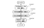
ここで、従来のアプリケーション処理における前述の不揮発性メモリとしてのEEPROMと揮発性メモリとしてのRAMとの間のデータの流れについて、図7のフローチャートに基づき、図8のブロック図を参照して説明する。
【0004】
図7において、ステップS401で、初期設定としてEEPROM16内に格納されたデータがRAM13内の記憶領域A131に転送され書写される(図8に示す処理(1)参照)。次にステップS402に移行して、EEPROM16に対して発生した書込みはRAM13内の記憶領域A131に対して実行される(図8に示す処理(3)参照)。次にステップS403に移行して、EEPROM16からのデータを読出すときにはそのデータが格納されているRAM13内の記憶領域A131から読出される(図8に示す処理(4)参照)。次にステップS404に移行して、イグニッションスイッチによる電源OFF時の終了処理でRAM13内に格納されている最新のデータがEEPROM16内に書戻され(図8に示す処理(2)参照)、本ルーチンを終了する。
【0005】
【発明が解決しようとする課題】
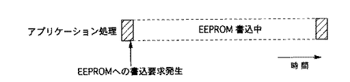
ところで、書換え可能な不揮発性メモリに記憶される前やその途中に、例えば、車両の盗難防止機能における暗証番号やダイアグノーシス(Diagnosis:故障診断)の診断結果のようなデータが電源上のトラブル等により壊れたり消えてしまうと車を始動させることができなくなったり、故障解析ができなくなるという不具合があった。ここで、不揮発性メモリへの書込処理をできるだけ短い周期で揮発性メモリ内のデータと比較しつつ、一致しないときには書換えすることが考えられるが、不揮発性メモリ(EEPROM)の書換時間は所定の制御対象を制御するためのプログラム実行時間に比べて長いため、図9のタイムチャートに示すように、書換中には他の処理が一時中断状態となってしまうことで、リアルタイム性が重要視される制御に対しては不具合が発生することとなる。
【0006】
そこで、この発明はかかる不具合を解決するためになされたもので、不揮発性メモリから揮発性メモリに転送されたデータに基づき所定の制御対象を制御する際、不揮発性メモリへの最新のデータの書戻要求があったときにはその制御に影響を与えることなく不揮発性メモリに確実に書戻し可能な車両用電子制御装置の提供を課題としている。
【0007】
【課題を解決するための手段】
請求項1の車両用電子制御装置によれば、書換可能な不揮発性メモリからのデータが書写された読書き可能な揮発性メモリのデータにより演算処理が実行されている際、不揮発性メモリにも直ちに書戻す必要のある新たなデータが発生したときには書込要求を発生するだけで元の処理が続行され、実際の書戻しは別の書込処理で実行される。このように、元の演算処理における中断は極めて短い時間でよいこととなる。これにより、重要なデータが電源の瞬断等のトラブルにより壊れたり消えてしまうことが防止され、リアルタイム性が重要視される制御が不都合なく実行できる。また、この制御手段では、書込要求として揮発性メモリの記憶領域に書戻すべきデータに対応した書込時に必要な付随データを書込むだけでよく、このための中断は極めて短い時間でよく、この処理とは別の書込処理によって直ちに書戻すべきデータをその書込時に必要な付随データに基づき不揮発性メモリに確実に書戻すことができる。
【0008】
請求項2の車両用電子制御装置の前記制御手段は、イグニッションスイッチによる電源OFF時の終了処理で揮発性メモリに格納されている最新のデータが不揮発性メモリに書戻されるものである。
請求項3の車両用電子制御装置の前記直ちに書戻すべきデータとは、車両の盗難防止機能における暗証番号である。
請求項4の車両用電子制御装置の前記直ちに書戻すべきデータとは、車両の故障診断の結果である。
【0009】
【発明の実施の形態】
以下、本発明の実施の形態を実施例に基づいて説明する。
【0010】
図1は本発明の実施の形態の一実施例にかかる車両用電子制御装置が適用され車両に搭載された内燃機関用電子制御装置の全体構成を示すブロック図である。
【0011】
図1において、10は内燃機関用電子制御装置(Electronic Control Unit;以下、単に、『ECU』と記す)であり、ECU10には、周知の中央処理装置としてCPU11、内燃機関用制御プログラム及びデータを格納する読出し専用の不揮発性メモリとしてのROM12、各種データを格納する読書き可能な揮発性メモリとしてのRAM13、それらを接続するアドレスバス14及びデータバス15等からなる論理演算回路としてのマイクロコンピュータ100が備えられている。そして、このマイクロコンピュータ100にはシリアル通信ラインを介して各種データを格納する書換可能な読出し専用の不揮発性メモリとしてのEEPROM(Electrically Erasable Programmable ROM: 電気的に書換可能な読出し専用メモリ)16が接続されている。
【0012】
また、ECU10には図示しない内燃機関の運転状態を検出する各種センサ1からのセンサ信号が入力される。これら各種センサ1からのセンサ信号はECU10内の入力回路17により波形整形処理、A/D変換処理等が実行されたのちマイクロコンピュータ100に入力される。マイクロコンピュータ100のCPU11では入力回路17からのセンサ信号に基づき内燃機関に対する最適な制御量が演算され、その演算結果としての制御信号が出力回路18に出力される。そして、出力回路18からの制御信号により内燃機関のイグナイタ21、インジェクタ(燃料噴射弁)22等のアクチュエータが駆動され、必要に応じて各種警告灯23が点灯される。また、車載の他のECU(例えば、盗難判定用ECU)30が、シリアルデータを入出力する入出力回路19Aを介してマイクロコンピュータ100に接続され、他のECU30とマイクロコンピュータ100との間でデータのやりとりが行われる。更に、ダイアグツール(故障診断装置)40が着脱可能にシリアル用入出力回路19Bを介してマイクロコンピュータ100に接続され、ダイアグツール40の接続時に故障診断に関するデータのやりとりが、ダイアグツール40とマイクロコンピュータ100との間で行われる。また、ECU10には車載バッテリ(図示略)からのバッテリ電圧+BをECU動作電圧5〔V〕に調整する電源回路50が備えられており、この動作電圧5〔V〕はマイクロコンピュータ100、入力回路17、出力回路18等に供給される。
【0013】
次に、本実施例のアプリケーション処理におけるEEPROM16とRAM13との間のデータの流れについて、図2に示すブロック図を参照して説明する。なお、RAM13内にはEEPROM16に格納された全データが転送され記憶される記憶領域A131とそのデータに対応した付随データとして書込時に必要なアドレス及びサイズが記憶される記憶領域B132とが形成されている。
【0014】
本実施例の図2のブロック図における処理(1)〜処理(4)は、前述の図8のブロック図における従来の処理(1)〜処理(4)と同様であるため、その詳細な説明を省略する。ここで、本実施例の図2では、アプリケーション処理による処理(3)と同時に実行される処理(5)及びEEPROM書込処理による処理(6)、処理(7)が追加されている。
【0015】
本実施例では、EEPROM16内へのEEPROM書込要求が発生されると図2に示す処理(3)が実行され、そのデータがRAM13の記憶領域A131に書込まれると同時に、図2に示す処理(5)が実行されEEPROM書込処理が必要とするデータに対応した付随データとして、EEPROM16への書込起動時に必要なアドレス及びサイズがRAM13の記憶領域B132にセットされる。
【0016】
次に、本発明の実施の形態の一実施例にかかる車両用電子制御装置で使用されているCPU11のアプリケーション処理によるEEPROM書込要求時の処理手順を示す図3のフローチャートに基づいて説明する。
【0017】
図3において、ステップS101で、データがRAM13の記憶領域A131に書込まれる。次にステップS102に移行して、RAM13内の記憶領域A131に書込まれたデータに対応した付随データとして、後述のEEPROM16への書込起動時に必要なアドレスが同じRAM13内の記憶領域B132にセットされる。次にステップS103に移行して、RAM13内の記憶領域A131に書込まれたデータに対応した付随データとして、後述のEEPROM16への書込起動時に必要なサイズが同じRAM13内の記憶領域B132にセットされ、本ルーチンを終了する。こののち、アプリケーション処理に戻り、残りのアプリケーション処理が実行される。
【0018】
ここで、CPU11のアプリケーション処理と並行して実行される実際のEEPROM16に対するEEPROM書込処理である図2に示す処理(7)は、図4及び図5に示す別の処理にて実行される。
【0019】
まず、EEPROM書込処理におけるEEPROM16に対する書込起動時の処理手順を示す図4のフローチャートに基づき、図6のタイムチャートを参照して説明する。なお、このルーチンはEEPROM16への書込要求が発生された際、書込要求のアプリケーション処理とは別のEEPROM書込処理でRAM13内の記憶領域B132に付随データが書込まれていると起動される。
【0020】
図4において、ステップS201で書込許可コマンドがEEPROM16に送信され、EEPROM16への書込みが許可状態とされる。次にステップS202に移行して、RAM13内の記憶領域B132にセットされている付随データとしてのアドレス及びサイズ(図2に示す処理(6)参照)に基づき書込コマンドがEEPROM16に送信され、本ルーチンを終了する。こののち、図6に示すように、EEPROM書込中としてRAM13の記憶領域A131に格納されている最新のデータの実際の書込みが実行される。
【0021】
ここで、上記処理は書込要求のアプリケーション処理よりも優先レベルの高い処理に定義されており、アプリケーション処理が一時中断され実行されるか、または所定の周期毎に書込要求が確認されると実行される。なお、所定の周期毎に起動される場合には、EEPROM16の書込時間より長い周期で起動されなければならない。例えば、EEPROM16の書込みに10msかかる場合には、この処理は10msよりも長い周期、例えば、16ms毎に起動されるようにする。これは、EEPROM16の書込時間より短い周期に設定されることで、前回の書込みが終了していないうちに新たな書込みが起動されるような不具合を防止するためである。
【0022】
次に、EEPROM書込処理におけるEEPROM16に対する書込終了時の処理手順を示す図5のフローチャートに基づき、図6のタイムチャートを参照して説明する。なお、このルーチンは、図6に示すように、上述の図4による書込起動処理ののちEEPROM書込中として実際の書込みが実行され(図2に示す処理(7)参照)、EEPROM16への書込みが終了すると起動される。
【0023】
図5において、ステップS301で書込禁止コマンドがEEPROM16に送信され、EEPROM16に対する書込みが禁止状態とされる。次にステップS302に移行して、読出コマンドがEEPROM16に送信され、EEPROM16に書込まれたデータが正しく書込まれているかがチェックされ、本ルーチンを終了する。ここで、上記処理は書込みの終了割込により実行してもよく、または書込起動から書込終了までの時間経過後に起動してもよい。
【0024】
このように、本実施例のECU10は、書換可能な不揮発性メモリとしてのEEPROM16及び読書き可能な揮発性メモリとしてのRAM13と、EEPROM16に記憶されたデータをRAM13に書写し、RAM13のデータを読出し演算処理して書込んだRAM13のデータを所定のタイミングでEEPROM16に書戻すCPU11にて達成される制御手段とを具備し、前記制御手段は、演算処理されたデータをRAM13に書込む際、そのデータがEEPROM16にも直ちに書戻すべきデータであるときには、同時に書込要求を発生させ、この書込要求に応じた別の書込処理にて書戻すべきデータをEEPROM16に書戻すものである。
【0025】
したがって、EEPROM16からのデータが書写されたRAM13のデータにより所定の制御対象を制御するためのアプリケーション処理が実行されている際、EEPROM16にも直ちに書戻す必要のある新たなデータが発生したときにはアプリケーション処理側では書込要求を発生させるだけでよく、実際の書戻しは別の書込処理で実行されるためアプリケーション処理の中断は極めて短い時間でよいこととなる。これにより、重要なデータが電源の瞬断等のトラブルにより壊れたり消えてしまうことが防止され、リアルタイム性が重要視される制御が不都合なく実行されることとなる。
【0026】
また、本実施例のECU10は、CPU11にて達成される制御手段が、書込要求にてRAM13の記憶領域B132に書戻すべきデータに対応して書込時に必要な付随データとしてのアドレス及びサイズを書込むと共に、別のEEPROM書込処理によって付随データとしてのアドレス及びサイズに基づき書戻すべきデータをEEPROM16に書戻すものである。
【0027】
即ち、所定の制御対象を制御するためのアプリケーション処理による書込要求としては、RAM13の記憶領域B132に書戻すべきデータに対応した付随データであるアドレス及びサイズを書込むだけでよい。これにより、アプリケーション処理の中断は極めて短い時間となり、その処理とは別のEEPROM書込処理によって書戻すべきデータがその書込時に必要なアドレス及びサイズに基づきEEPROM16に確実に書戻されることとなる。
【図面の簡単な説明】
【図1】 図1は本発明の実施の形態の一実施例にかかる車両用電子制御装置が適用され車両に搭載されたECUの全体構成を示すブロック図である。
【図2】 図2は本発明の実施の形態の一実施例にかかる車両用電子制御装置で使用されているECU内のCPUにおけるアプリケーション処理及びEEPROM書込処理によるEEPROMとRAMとの間のデータの流れを示すブロック図である。
【図3】 図3は本発明の実施の形態の一実施例にかかる車両用電子制御装置で使用されているECU内のCPUにおけるEEPROM書込要求時の処理手順を示すフローチャートである。
【図4】 図4は本発明の実施の形態の一実施例にかかる車両用電子制御装置で使用されているECU内のCPUにおけるEEPROMに対する書込起動時の処理手順を示すフローチャートである。
【図5】 図5は本発明の実施の形態の一実施例にかかる車両用電子制御装置で使用されているECU内のCPUにおけるEEPROMに対する書込終了時の処理手順を示すフローチャートである。
【図6】 図6は本発明の実施の形態の一実施例にかかる車両用電子制御装置で使用されているECU内のCPUにおけるアプリケーション処理及びEEPROM書込処理を示すタイムチャートである。
【図7】 図7は従来のアプリケーション処理におけるEEPROMとRAMとの間のデータの処理手順を示すフローチャートである。
【図8】 図8は従来のアプリケーション処理におけるEEPROMとRAMとの間のデータの流れを示すブロック図である。
【図9】 図9は従来のアプリケーション処理を示すタイムチャートである。
【符号の説明】
1 各種センサ
10 ECU(内燃機関用電子制御装置)
11 CPU(制御手段)
13 RAM(読書き可能な揮発性メモリ)
131 記憶領域A
132 記憶領域B
16 EEPROM(書換可能な不揮発性メモリ)[0001]
BACKGROUND OF THE INVENTION
The present invention relates to a vehicle electronic control device that always stores the latest data in a rewritable nonvolatile memory.
[0002]
[Prior art]
Conventionally, the data stored in the rewritable non-volatile memory at the initial setting when the power is turned on is transferred to the readable / writable volatile memory and copied, and a predetermined control object is determined based on the data in the volatile memory. There is known an electronic control device that has a processing procedure of controlling and writing the latest data in a volatile memory back to a nonvolatile memory when the power is turned off. This is a process for coping with the fact that the nonvolatile memory has a limited number of times of rewriting and the data cannot be rewritten many times as in the case of the volatile memory.
[0003]
Here, the flow of data between the EEPROM as the nonvolatile memory and the RAM as the volatile memory in the conventional application processing will be described with reference to the block diagram of FIG. 8 based on the flowchart of FIG. .
[0004]
In FIG. 7, in step S401, the data stored in the
[0005]
[Problems to be solved by the invention]
By the way, before or during storage in the rewritable nonvolatile memory, for example, data such as a security code in the vehicle anti-theft function or diagnosis result of diagnosis (power failure diagnosis) If it breaks or disappears, the car cannot be started or failure analysis cannot be performed. Here, it is conceivable that the writing process to the non-volatile memory is compared with the data in the volatile memory in the shortest possible cycle and is rewritten when they do not match, but the rewriting time of the non-volatile memory (EEPROM) Since it is longer than the program execution time for controlling the controlled object, as shown in the time chart of FIG. 9, the real-time property is regarded as important because other processes are temporarily suspended during rewriting. This causes a problem with the control.
[0006]
Accordingly, the present invention has been made to solve such a problem. When a predetermined control target is controlled based on data transferred from the nonvolatile memory to the volatile memory, the latest data is written to the nonvolatile memory. An object of the present invention is to provide a vehicular electronic control device that can reliably write back to a non-volatile memory without affecting the control when a return request is made.
[0007]
[Means for Solving the Problems]
According to the vehicle electronic control device of the first aspect, when the arithmetic processing is executed by the data in the readable / writable volatile memory in which the data from the rewritable nonvolatile memory is copied, the nonvolatile memory also has When new data that needs to be written back immediately occurs, the original process is continued only by generating a write request, and the actual write-back is executed in another write process. As described above, the interruption in the original arithmetic processing is very short. As a result, it is possible to prevent important data from being broken or lost due to troubles such as a momentary power interruption, and control in which real-time property is regarded as important can be executed without any inconvenience. Further, in this control means, it is only necessary to write the accompanying data necessary at the time of writing corresponding to the data to be written back to the storage area of the volatile memory as a writing request, and the interruption for this may be an extremely short time, Data to be immediately written back by a writing process different from this process can be surely written back to the nonvolatile memory based on the accompanying data required at the time of writing.
[0008]
The control means of the vehicle electronic control device according to the second aspect is such that the latest data stored in the volatile memory is written back to the non-volatile memory in the termination process when the power is turned off by the ignition switch.
The data to be immediately written back in the vehicle electronic control device according to claim 3 is a personal identification number in the antitheft function of the vehicle.
The data to be immediately written back by the vehicle electronic control device according to
[0009]
DETAILED DESCRIPTION OF THE INVENTION
Hereinafter, embodiments of the present invention will be described based on examples.
[0010]
Figure 1 is a block diagram showing the overall construction of the embodiment of the internal combustion engine electronic control unit mounted on the vehicle is a vehicle electronic control device applied according to an embodiment of the present invention.
[0011]
In FIG. 1,
[0012]
The ECU 10 receives sensor signals from
[0013]
Next, the flow of data between the
[0014]
The processing (1) to processing (4) in the block diagram of FIG. 2 of the present embodiment is the same as the conventional processing (1) to processing (4) in the block diagram of FIG. Is omitted. Here, in FIG. 2 of the present embodiment, processing (5) executed simultaneously with processing (3) by application processing, processing (6) and processing (7) by EEPROM writing processing are added.
[0015]
In the present embodiment, when an EEPROM write request to the
[0016]
Next, a description will be given based on the flowchart of FIG. 3 showing a processing procedure at the time of an EEPROM write request by application processing of the CPU 11 used in the vehicle electronic control apparatus according to an example of the embodiment of the present invention.
[0017]
In FIG. 3, in step S <b> 101, data is written into the storage area A <b> 131 of the
[0018]
Here, the process (7) shown in FIG. 2 which is the EEPROM writing process to the
[0019]
First, based on the flowchart of FIG. 4 which shows the processing procedure at the time of starting writing to the
[0020]
In FIG. 4, a write permission command is transmitted to the
[0021]
Here, the above process is defined as a process having a higher priority level than the application process of the write request, and when the application process is temporarily interrupted and executed or when the write request is confirmed at a predetermined cycle Executed. In addition, when starting at every predetermined cycle, it must be started at a cycle longer than the writing time of the
[0022]
Next, description will be made with reference to the time chart of FIG. 6 based on the flowchart of FIG. 5 showing the processing procedure at the end of writing to the
[0023]
In FIG. 5, a write inhibit command is transmitted to the
[0024]
As described above, the
[0025]
Therefore, when an application process for controlling a predetermined control object is executed by the data in the
[0026]
Further, the
[0027]
That is, as a write request by an application process for controlling a predetermined control target, it is only necessary to write an address and size that are accompanying data corresponding to data to be written back to the storage area B132 of the
[Brief description of the drawings]
FIG. 1 is a block diagram showing an overall configuration of an ECU mounted on a vehicle to which a vehicle electronic control device according to an example of an embodiment of the present invention is applied.
FIG. 2 is a diagram showing data between an EEPROM and a RAM by an application process and an EEPROM write process in a CPU in an ECU used in an electronic control device for a vehicle according to an example of an embodiment of the present invention; It is a block diagram which shows the flow.
FIG. 3 is a flowchart showing a processing procedure when an EEPROM write request is made in a CPU in an ECU used in the vehicle electronic control device according to an embodiment of the present invention;
FIG. 4 is a flowchart showing a processing procedure at the start of writing to the EEPROM in the CPU in the ECU used in the electronic control device for a vehicle according to an example of the embodiment of the present invention;
FIG. 5 is a flowchart showing a processing procedure at the end of writing to the EEPROM in the CPU in the ECU used in the vehicle electronic control apparatus according to an embodiment of the present invention;
FIG. 6 is a time chart showing application processing and EEPROM writing processing in a CPU in the ECU used in the vehicle electronic control apparatus according to an embodiment of the present invention.
FIG. 7 is a flowchart showing a data processing procedure between an EEPROM and a RAM in conventional application processing.
FIG. 8 is a block diagram showing a data flow between an EEPROM and a RAM in conventional application processing.
FIG. 9 is a time chart showing conventional application processing.
[Explanation of symbols]
1
11 CPU (control means)
13 RAM (volatile memory that can be read and written)
131 Storage area A
132 Storage area B
16 EEPROM (Rewritable non-volatile memory)
Claims (4)
前記制御手段は、アプリケーション処理により演算処理されたデータを前記揮発性メモリに書込む際、前記データが前記不揮発性メモリにも直ちに書戻すべきデータであるときには、同時に書込要求を発生させ、この書込要求にて前記揮発性メモリの所定の記憶領域に前記書戻すべきデータに対応して、書込時に必要な付随データを書込むと共に、前記アプリケーション処理に戻るものであって、
前記制御手段は、前記書戻すべきデータの前記不揮発性メモリへ書戻す書込処理を、前記付随データに基づき、前記アプリケーション処理と平行して行われる別の処理として実行するものであることを特徴とする車両用電子制御装置。The rewritable nonvolatile memory and the readable / writable volatile memory, and the data stored in the nonvolatile memory are copied to the volatile memory, and the data in the volatile memory is read and processed and written. Control means for writing back the data of the volatile memory to the nonvolatile memory at a predetermined timing,
Wherein, when writing operation processing data by an application process in the volatile memory, when the data is data to be returned immediately written to the nonvolatile memory, generates a write request at the same time, this Corresponding to the data to be written back to the predetermined storage area of the volatile memory by a write request, the accompanying data necessary at the time of writing is written, and the process returns to the application process,
The control means executes the writing process of writing back the data to be written back to the nonvolatile memory as another process performed in parallel with the application process based on the accompanying data. An electronic control device for a vehicle.
Priority Applications (3)
| Application Number | Priority Date | Filing Date | Title |
|---|---|---|---|
| JP18580498A JP4135220B2 (en) | 1998-07-01 | 1998-07-01 | Electronic control device for vehicle |
| US09/321,585 US6401163B1 (en) | 1998-07-01 | 1999-05-28 | Apparatus and method for rewriting data from volatile memory to nonvolatile memory |
| DE19929796A DE19929796B4 (en) | 1998-07-01 | 1999-06-29 | Apparatus and method for rewriting data from a volatile memory to a nonvolatile memory |
Applications Claiming Priority (1)
| Application Number | Priority Date | Filing Date | Title |
|---|---|---|---|
| JP18580498A JP4135220B2 (en) | 1998-07-01 | 1998-07-01 | Electronic control device for vehicle |
Publications (2)
| Publication Number | Publication Date |
|---|---|
| JP2000020407A JP2000020407A (en) | 2000-01-21 |
| JP4135220B2 true JP4135220B2 (en) | 2008-08-20 |
Family
ID=16177189
Family Applications (1)
| Application Number | Title | Priority Date | Filing Date |
|---|---|---|---|
| JP18580498A Expired - Fee Related JP4135220B2 (en) | 1998-07-01 | 1998-07-01 | Electronic control device for vehicle |
Country Status (3)
| Country | Link |
|---|---|
| US (1) | US6401163B1 (en) |
| JP (1) | JP4135220B2 (en) |
| DE (1) | DE19929796B4 (en) |
Families Citing this family (21)
| Publication number | Priority date | Publication date | Assignee | Title |
|---|---|---|---|---|
| DE19954258A1 (en) * | 1999-11-11 | 2001-05-17 | Truetzschler Gmbh & Co Kg | Device for the electronic control of spinning machines, in particular spinning preparation machines |
| US6785764B1 (en) * | 2000-05-11 | 2004-08-31 | Micron Technology, Inc. | Synchronous flash memory with non-volatile mode register |
| JP3641448B2 (en) * | 2001-09-06 | 2005-04-20 | 松下電器産業株式会社 | Arithmetic processing unit |
| KR100450080B1 (en) * | 2001-11-13 | 2004-10-06 | (주)지에스텔레텍 | Portable storage medium based on Universal Serial Bus standard and Control Method therefor |
| US6788605B2 (en) * | 2002-07-15 | 2004-09-07 | Hewlett-Packard Development Company, L.P. | Shared volatile and non-volatile memory |
| JP2004063004A (en) * | 2002-07-29 | 2004-02-26 | Sony Corp | Compound memory circuit structure and semiconductor device having the same |
| US6901298B1 (en) * | 2002-09-30 | 2005-05-31 | Rockwell Automation Technologies, Inc. | Saving and restoring controller state and context in an open operating system |
| JP2004152279A (en) * | 2002-10-08 | 2004-05-27 | Matsushita Electric Ind Co Ltd | Program updating method, and terminal device |
| US6959370B2 (en) * | 2003-01-03 | 2005-10-25 | Hewlett-Packard Development Company, L.P. | System and method for migrating data between memories |
| US7168002B2 (en) * | 2003-04-25 | 2007-01-23 | International Business Machines Corporation | Preservation of error data on a diskless platform |
| CA2479868A1 (en) * | 2003-09-02 | 2005-03-02 | Ronald E. Brick | Light fixture |
| CN101091222A (en) * | 2004-10-26 | 2007-12-19 | 斯班逊有限公司 | Nonvolatile storage device |
| US7622834B2 (en) * | 2005-09-22 | 2009-11-24 | Nidec Corporation | Brushless DC motor and manufacturing method thereof |
| JP4736828B2 (en) * | 2006-02-03 | 2011-07-27 | 株式会社デンソー | Electronic control unit |
| US7436708B2 (en) * | 2006-03-01 | 2008-10-14 | Micron Technology, Inc. | NAND memory device column charging |
| US7869275B2 (en) * | 2006-10-07 | 2011-01-11 | Active-Semi, Inc. | Memory structure capable of bit-wise write or overwrite |
| EP2026288A3 (en) * | 2007-08-03 | 2010-11-24 | Denso Corporation | Electronic control system and method for vehicle diagnosis |
| JP4345860B2 (en) | 2007-09-14 | 2009-10-14 | 株式会社デンソー | Vehicle memory management device |
| DE102009046518A1 (en) * | 2009-11-09 | 2011-05-12 | Robert Bosch Gmbh | memory array |
| JP5880192B2 (en) * | 2012-03-23 | 2016-03-08 | スズキ株式会社 | Storage control device, storage control method and program |
| JP6365346B2 (en) * | 2015-02-27 | 2018-08-01 | 京セラドキュメントソリューションズ株式会社 | Information processing apparatus and memory management program |
Family Cites Families (14)
| Publication number | Priority date | Publication date | Assignee | Title |
|---|---|---|---|---|
| US4959774A (en) * | 1984-07-06 | 1990-09-25 | Ampex Corporation | Shadow memory system for storing variable backup blocks in consecutive time periods |
| JPS637063A (en) * | 1986-06-27 | 1988-01-12 | Fujitsu Ltd | Data backup system |
| US5023813A (en) * | 1989-08-03 | 1991-06-11 | International Business Machines Corporation | Non-volatile memory usage |
| JPH0833862B2 (en) * | 1989-10-23 | 1996-03-29 | インターナシヨナル・ビジネス・マシーンズ・コーポレーシヨン | Object-oriented computer system |
| JPH05289949A (en) | 1992-04-09 | 1993-11-05 | Nippondenso Co Ltd | Vehicle control device |
| US5719988A (en) * | 1994-05-31 | 1998-02-17 | Tektronix, Inc. | Dynamically paged non-volatile random access video store |
| US5682471A (en) * | 1994-10-06 | 1997-10-28 | Billings; Thomas Neal | System for transparently storing inputs to non-volatile storage and automatically re-entering them to reconstruct work if volatile memory is lost |
| KR100204027B1 (en) * | 1996-02-16 | 1999-06-15 | 정선종 | Database recovery apparatus and method using nonvolatile memory |
| US5708589A (en) * | 1996-04-08 | 1998-01-13 | Vaughn Manufacturing Corporation | Error recovery system for an energy controller for an electric water heater |
| GB2317721B (en) * | 1996-09-30 | 2001-09-12 | Nokia Mobile Phones Ltd | Memory device |
| JP3166634B2 (en) * | 1996-11-07 | 2001-05-14 | 日産自動車株式会社 | Fault storage device for vehicle control unit |
| US5884211A (en) * | 1997-01-23 | 1999-03-16 | Ford Global Technologies, Inc. | System and method for memory reset of a vehicle controller |
| DE19740525C1 (en) * | 1997-09-15 | 1999-02-04 | Siemens Ag | Method of data storage and recovery in control system, esp. in motor vehicle, such as taxi |
| US6091658A (en) * | 1999-11-01 | 2000-07-18 | Ford Global Technologies, Inc. | Nonvolatile memory implementation for electronic devices |
-
1998
- 1998-07-01 JP JP18580498A patent/JP4135220B2/en not_active Expired - Fee Related
-
1999
- 1999-05-28 US US09/321,585 patent/US6401163B1/en not_active Expired - Lifetime
- 1999-06-29 DE DE19929796A patent/DE19929796B4/en not_active Expired - Fee Related
Also Published As
| Publication number | Publication date |
|---|---|
| JP2000020407A (en) | 2000-01-21 |
| DE19929796A1 (en) | 2000-01-05 |
| US6401163B1 (en) | 2002-06-04 |
| DE19929796B4 (en) | 2011-04-07 |
Similar Documents
| Publication | Publication Date | Title |
|---|---|---|
| JP4135220B2 (en) | Electronic control device for vehicle | |
| JP4340297B2 (en) | Memory rewriting system for vehicle control device | |
| JP3822658B2 (en) | Control device | |
| JP4539757B2 (en) | Electronic control unit | |
| JP5176728B2 (en) | Electronic control device for vehicle | |
| US8095263B2 (en) | Electronic control unit and vehicle control system | |
| JP3893755B2 (en) | Electronic control unit | |
| JP3969278B2 (en) | Electronic control unit | |
| US6182004B1 (en) | Apparatus and method for controlling electric power supply in nonvolatile memory rewriting operation | |
| JP3726295B2 (en) | Vehicle control device | |
| JP2009042850A (en) | Control device for vehicle, and device for updating vehicle control program | |
| JP3883842B2 (en) | Electronic control device for vehicle | |
| US6907495B2 (en) | Rewriting system for rewriting a memory on a vehicle controller | |
| JP2002323902A (en) | Electronic controller | |
| JP2004164601A (en) | Electronic controller | |
| JP2002041367A (en) | Vehicle controller | |
| JP2005338955A (en) | Electronic control device | |
| JPH11141391A (en) | Controller for automobile | |
| JPH1083294A (en) | Operating method for controller equipped with storage device programmable through programming device | |
| JP2003104138A (en) | System for monitoring vehicle control device for rewriting of data | |
| US6490663B1 (en) | Electronic control apparatus having rewritable nonvolatile memory | |
| JPH08247011A (en) | Electronic control device for automobile | |
| JPH05289949A (en) | Vehicle control device | |
| JP2001182607A (en) | Vehicle controlling device | |
| JPH0793006A (en) | Electronic control unit for vehicle |
Legal Events
| Date | Code | Title | Description |
|---|---|---|---|
| A621 | Written request for application examination |
Free format text: JAPANESE INTERMEDIATE CODE: A621 Effective date: 20041227 |
|
| A977 | Report on retrieval |
Free format text: JAPANESE INTERMEDIATE CODE: A971007 Effective date: 20070801 |
|
| A131 | Notification of reasons for refusal |
Free format text: JAPANESE INTERMEDIATE CODE: A131 Effective date: 20070807 |
|
| A521 | Request for written amendment filed |
Free format text: JAPANESE INTERMEDIATE CODE: A523 Effective date: 20071005 |
|
| A131 | Notification of reasons for refusal |
Free format text: JAPANESE INTERMEDIATE CODE: A131 Effective date: 20080212 |
|
| A521 | Request for written amendment filed |
Free format text: JAPANESE INTERMEDIATE CODE: A523 Effective date: 20080410 |
|
| TRDD | Decision of grant or rejection written | ||
| A01 | Written decision to grant a patent or to grant a registration (utility model) |
Free format text: JAPANESE INTERMEDIATE CODE: A01 Effective date: 20080513 |
|
| A01 | Written decision to grant a patent or to grant a registration (utility model) |
Free format text: JAPANESE INTERMEDIATE CODE: A01 |
|
| A61 | First payment of annual fees (during grant procedure) |
Free format text: JAPANESE INTERMEDIATE CODE: A61 Effective date: 20080526 |
|
| R150 | Certificate of patent or registration of utility model |
Free format text: JAPANESE INTERMEDIATE CODE: R150 |
|
| FPAY | Renewal fee payment (event date is renewal date of database) |
Free format text: PAYMENT UNTIL: 20110613 Year of fee payment: 3 |
|
| FPAY | Renewal fee payment (event date is renewal date of database) |
Free format text: PAYMENT UNTIL: 20110613 Year of fee payment: 3 |
|
| FPAY | Renewal fee payment (event date is renewal date of database) |
Free format text: PAYMENT UNTIL: 20120613 Year of fee payment: 4 |
|
| FPAY | Renewal fee payment (event date is renewal date of database) |
Free format text: PAYMENT UNTIL: 20120613 Year of fee payment: 4 |
|
| FPAY | Renewal fee payment (event date is renewal date of database) |
Free format text: PAYMENT UNTIL: 20130613 Year of fee payment: 5 |
|
| FPAY | Renewal fee payment (event date is renewal date of database) |
Free format text: PAYMENT UNTIL: 20140613 Year of fee payment: 6 |
|
| R250 | Receipt of annual fees |
Free format text: JAPANESE INTERMEDIATE CODE: R250 |
|
| R250 | Receipt of annual fees |
Free format text: JAPANESE INTERMEDIATE CODE: R250 |
|
| R250 | Receipt of annual fees |
Free format text: JAPANESE INTERMEDIATE CODE: R250 |
|
| LAPS | Cancellation because of no payment of annual fees |