JP4135083B2 - Image signal processing apparatus and processing method, and image display apparatus using the same - Google Patents
Image signal processing apparatus and processing method, and image display apparatus using the same Download PDFInfo
- Publication number
- JP4135083B2 JP4135083B2 JP2003057638A JP2003057638A JP4135083B2 JP 4135083 B2 JP4135083 B2 JP 4135083B2 JP 2003057638 A JP2003057638 A JP 2003057638A JP 2003057638 A JP2003057638 A JP 2003057638A JP 4135083 B2 JP4135083 B2 JP 4135083B2
- Authority
- JP
- Japan
- Prior art keywords
- image signal
- pixel data
- signal
- target position
- maximum value
- Prior art date
- Legal status (The legal status is an assumption and is not a legal conclusion. Google has not performed a legal analysis and makes no representation as to the accuracy of the status listed.)
- Expired - Fee Related
Links
Images








Landscapes
- Image Processing (AREA)
- Picture Signal Circuits (AREA)
- Controls And Circuits For Display Device (AREA)
Description
【0001】
【発明の属する技術分野】
この発明は、例えば画像信号の高域を強調するエンハンサ、画像信号の画素数を変換するスケーリング装置等に適用して好適な画像信号の処理装置および処理方法、並びにそれを利用した画像表示装置に関する。
【0002】
詳しくは、この発明は、処理後の画像信号における注目位置の画素データの値が、処理前の画像信号の注目位置の近傍の画素データの最大値より大きいとき、または最小値より小さいとき、処理後の画像信号における注目位置の画素データの値を、当該注目位置の近傍の波形の複雑さの度合いが低い程最大値または最小値に近づくように抑圧して出力画像信号を得ることによって、例えばエンハンス処理やスケーリング処理等を行った場合に、何等不都合を発生することなく、エッジ部分の画質改善を図るようにした画像信号処理装置等に係るものである。
【0003】
【従来の技術】
従来、画像の輪郭を強調するためのエンハンサが種々提案されている(特許文献1参照)。
図19は、従来のエンハンサ200の構成例を示している。
このエンハンサ200は、入力画像信号としての画像信号Vaを入力する入力端子201と、この画像信号Vaから垂直方向の高域成分を垂直輪郭信号として抽出する垂直ハイパスフィルタ(垂直HPF)202と、この輪郭信号に非線形特性を付与する非線形特性回路203と、入力端子201に入力された画像信号Vaに非線形特性回路203で非線形特性が付与された輪郭信号を加算して、垂直方向の高域が強調された画像信号V21を得る加算器204と、オーバフローおよびアンダーフローを防止するために、加算器204で得られる画像信号V21の振幅を制限するリミッタ205とを有している。
【0004】
また、エンハンサ200は、入力端子201に入力された画像信号Vaから水平方向の高域成分を水平輪郭信号として抽出する水平ハイパスフィルタ(水平HPF)206と、この輪郭信号に非線形特性を付与する非線形特性回路207と、リミッタ205で振幅制限されて得られた画像信号V22に非線形特性回路207で非線形特性が付与された輪郭信号を加算して、垂直方向および水平方向の高域が強調された画像信号V23を得る加算器208と、オーバフローおよびアンダーフローを防止するために、加算器208で得られる画像信号V23の振幅を制限するリミッタ209と、このリミッタ209から出力される画像信号Vbを出力画像信号として出力する出力端子210とを有している。
【0005】
非線形特性回路203,207は、それぞれ、入力信号の絶対値レベルが所定値以下であるとき、出力信号のレベルを0とする。これにより、ノイズ成分が強調されることが防止される。また、非線形特性回路203,207は、それぞれ、入力信号の絶対値レベルが所定値以上であるとき、出力信号のレベルを一定値とする。これにより、高域の信号レベルが飽和することが防止される。
【0006】
図19に示すエンハンサ200の動作を説明する。
画像信号Vaが入力端子201に入力される。この画像信号Vaは垂直ハイパスフィルタ202に供給される。この垂直ハイパスフィルタ202では、画像信号Vaから垂直方向の高域成分が垂直輪郭信号として抽出される。この垂直輪郭信号は非線形特性回路203を介して加算器204に供給される。
【0007】
この加算器204には、入力端子201に入力された画像信号Vaも供給される。加算器204では、画像信号Vaに垂直輪郭信号が加算され、垂直方向の高域が強調された画像信号V21が得られる。この画像信号V21はリミッタ205に供給される。このリミッタ205では、画像信号V21の振幅が制限され、オーバフローおよびアンダーフローが防止される。
【0008】
また、入力端子201に入力された画像信号Vaは水平ハイパスフィルタ206に供給される。この水平ハイパスフィルタ206では、画像信号Vaから水平方向の高域成分が水平輪郭信号として抽出される。この水平輪郭信号は非線形特性回路207を介して加算器208に供給される。
【0009】
この加算器208には、リミッタ205から出力される画像信号V22も供給される。加算器208では、画像信号V22に水平輪郭信号が加算され、垂直方向および水平方向の高域が強調された画像信号V23が得られる。この画像信号V23はリミッタ209に供給される。このリミッタ209では、画像信号V23の振幅が制限され、オーバフローおよびアンダーフローが防止される。そして、このリミッタ209から出力される画像信号Vbが出力端子210に出力される。
【0010】
この画像信号Vbは、上述したように垂直方向および水平方向の高域が強調されたものである。そのため、この画像信号Vbによる画像は、垂直方向および水平方向の輪郭が強調されて、鮮鋭感が出たものとなる。
【0011】
【特許文献1】
特開2002−77667号公報
【0012】
【発明が解決しようとする課題】
ここで、入力画像信号Vaと出力画像信号Vbについて説明する。図20、図21は、横軸を垂直方向または水平方向のサンプル点とし、縦軸をその各サンプル点に対応した画素データのレベルを示している。
【0013】
画像信号Vaが図20Aに示すようにエッジと平坦な部分のある信号であるとき、画像信号Vbは図20Bに示すようになり、エッジ部分は急峻になるが、このエッジ部分近くの平坦な部分のレベルが変化する。このレベル変化のために、画像のエッジ部分の両側に縁取りが発生する。
【0014】
このように画像信号Vbにおいて、エッジ部分近くの平坦な部分のレベルが変化するのは、画像信号Vaが図22Aに示すようにエッジと平坦な部分のある信号であるとき、この画像信号Vaから抽出される高域成分である輪郭信号は図22Bに示すようになる。したがって、画像信号Vaに輪郭信号を加算して得られる画像信号Vbは図22Cに示すようにエッジ部分は急峻になるが、このエッジ部分近くの平坦な部分のレベルが変化したものとなる。
【0015】
ここで、輪郭信号としての高域成分を抽出するハイパスフィルタのタップ数を多くすることで、その高域成分の低域側のレベルを持ち上げることができる。そのため、画像信号Vaのエッジ部分をより急峻にでき、画像の輪郭をより強調できる。しかし、レベルが変化するエッジ部分近くの平坦な部分の範囲が広くなり、画像のエッジ部分の両側に発生する縁取りが広くなり、この縁取りがより目立つものとなる(図22B,Cの破線部分参照)。
【0016】
したがって従来、画像のエッジ部分の両側に発生する縁取りが目立たなくするため、輪郭信号としての高域成分を抽出するハイパスフィルタのタップ数を多くすることができず、画像の輪郭強調の効果を充分に得ることが困難であった。
【0017】
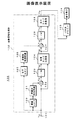
図20Bに示す画像信号Vbの場合には、図20Cに示すように、エッジ部分は急峻のままで、このエッジ部分近くの平坦な部分のレベル変化をなくした画像信号とすることができれば、画像の輪郭を強調でき、かつエッジ部分の両側に縁取りが発生することはなく、理想的である。
【0018】
なお、画像信号Vaが図21Aに示すように平坦な部分のない信号であるとき、画像信号Vbは図21Bに示すようになる。この場合、ユーザは画像に縁取りを感じることはない。したがってこの場合には、図21Cに示すように、画像信号Vbと同じ画像信号とすることができれば、理想的である。
【0019】
上述した特許文献1には、輝度信号の低域成分を周辺輝度信号として抽出し、この周辺輝度信号が第1のレベルより高くなったとき、およびこの周辺輝度信号が第2のレベルより低くなったとき、輪郭信号の振幅を抑圧し、適切な輪郭強調効果を得ることが記載されている。
【0020】
しかし、このように周辺輝度信号のレベルに応じて輪郭信号の振幅を抑圧するものでは、周辺輝度信号のレベルが第1のレベルより高くない場合、あるいは第2のレベルより低くない場合、輪郭信号の振幅の抑圧は行われず、上述したエッジ部分近くの平坦な部分のレベル変化を抑圧することはできない。
【0021】
したがってこの場合、図20Bに示す画像信号Vbを図20Cに示すような理想的な画像信号に近づけることはできず、画像のエッジ部分の両側の縁取りが目立つことを軽減できない。
【0022】
また、上述した特許文献1には、輪郭信号の絶対値レベルが大きいとき、当該輪郭信号の振幅を抑圧し、画像信号のエッジ部分のレベル差が大きい場合にも自然な輪郭強調効果を得ることが記載されている。
【0023】
この場合、画像信号のエッジ部分近くの平坦な部分のレベル変化を抑圧でき、画像のエッジ部分の両側の縁取りが目立つことを軽減できる。しかしこの場合、輪郭信号の絶対値レベルが大きいときは一律に輪郭信号の振幅を抑圧するものである。そのため、縁取りが目立たない画像信号のエッジ部分近くの平坦な部分以外でも、輪郭信号の絶対値レベルが大きいときは輪郭信号の振幅が抑圧され、輪郭強調効果が弱められるという問題がある。
【0024】
なお、水平方向および垂直方向の画素数を補間処理によって変換するスケーリング装置においては、画像信号のエッジ部分近くの平坦な部分でリンギングが発生し、これが画質劣化の要因となっている。
【0025】
この発明は、例えばエンハンス処理やスケーリング処理等を行った場合、何等不都合なく、エッジ部分の画質改善を図ることを目的とする。
【0026】
【課題を解決するための手段】
この発明に係る画像信号処理装置は、複数の画素データからなる第1の画像信号を処理して複数の画素データからなる第2の画像信号を得る画像信号処理手段と、第2の画像信号における注目位置の近傍に位置する、第1の画像信号の複数の画素データから平坦度を求め、当該平坦度に基づいて、波形の複雑さの度合いを判別する波形判別手段と、第2の画像信号における注目位置の近傍に位置する、第1の画像信号の複数の画素データの最大値を検出する最大値検出手段と、第2の画像信号における注目位置の近傍に位置する、第1の画像信号の複数の画素データの最小値を検出する最小値検出手段と、第2の画像信号における注目位置の画素データの値が、最大値検出手段で検出される最大値より大きいとき、または最小値検出手段で検出される最小値より小さいとき、波形判別手段の判別結果に基づき、第2の画像信号における注目位置の画素データの値を、波形の複雑さの度合いが低い程最大値または最小値に近づくように抑圧して第3の画像信号を得る信号抑圧手段とを備えるものである。
【0027】
また、この発明に係る画像信号処理方法は、複数の画素データからなる第1の画像信号を処理して複数の画素データからなる第2の画像信号を得るステップと、第2の画像信号における注目位置の近傍に位置する、第1の画像信号の複数の画素データから平坦度を求め、当該平坦度に基づいて、波形の複雑さの度合いを判別するステップと、第2の画像信号における注目位置の近傍に位置する、第1の画像信号の複数の画素データの最大値を検出するステップと、第2の画像信号における注目位置の近傍に位置する、第1の画像信号の複数の画素データの最小値を検出するステップと、第2の画像信号における注目位置の画素データの値が、検出される最大値より大きいとき、または検出される最小値より小さいとき、波形の複雑さの度合いの判別結果に基づき、第2の画像信号における注目位置の画素データの値を、波形の複雑さの度合いが低い程最大値または最小値に近づくように抑圧して第3の画像信号を得るステップとを備えるものである。
【0028】
また、この発明に係る画像表示装置は、複数の画素データからなる第1の画像信号を処理して複数の画素データからなる第2の画像信号を得る画像信号処理手段と、第2の画像信号における注目位置の近傍に位置する、第1の画像信号の複数の画素データから平坦度を求め、当該平坦度に基づいて、波形の複雑さの度合いを判別する波形判別手段と、第2の画像信号における注目位置の近傍に位置する、第1の画像信号の複数の画素データの最大値を検出する最大値検出手段と、第2の画像信号における注目位置の近傍に位置する、第1の画像信号の複数の画素データの最小値を検出する最小値検出手段と、第2の画像信号における注目位置の画素データの値が、最大値検出手段で検出される最大値より大きいとき、または最小値検出手段で検出される最小値より小さいとき、波形判別手段の判別結果に基づき、第2の画像信号における注目位置の画素データの値を、波形の複雑さの度合いが低い程最大値または最小値に近づくように抑圧して第3の画像信号を得る信号抑圧手段と、この信号抑圧手段で得られる第3の画像信号による画像を表示する表示素子とを備えるものである。
【0029】
この発明においては、複数の画素データからなる第1の画像信号が処理されて複数の画素データからなる第2の画像信号が得られる。
例えば、エンハンス処理(輪郭強調処理)が行われる。すなわち、第1の画像信号から高域成分が抽出され、この高域成分が第1の画像信号に加算されて高域を強調した第2の画像信号が得られる。この場合、画像信号のエッジ部分近くの平坦な部分のレベルが変化し、これが画質劣化の要因となる。
【0030】
また例えば、スケーリング処理(画素数変換処理)が行われる。すなわち、第1の画像信号に基づいて、少なくとも水平または垂直の補間方向における補間位置の画素データが生成され、この補間方向の画素数を変換した第2の画像信号が得られる。この場合、画像信号のエッジ部分近くの平坦な部分でリンギング(レベル変化)が発生し、これが画質劣化の要因となる。
【0031】
第2の画像信号における注目位置の近傍に位置する、第1の画像信号の複数の画素データに基づいて、波形の複雑さの度合いが判別される。この場合、例えば、画像信号のエッジ部分近くの平坦な部分は、波形の複雑さの度合いが低い、と判別されるようにする。
【0032】
例えば、少なくとも水平方向または垂直方向である所定方向に関して注目位置から一の側に位置する複数の画素データに基づいて平坦度を示す第1の信号が求められると共に、この所定方向に関して注目位置から他の側に位置する複数の画素データに基づいて平坦度を示す第2の信号を求められ、これら第1の信号および第2の信号のうち小さな値の信号に基づいて判別結果が得られる。
【0033】
第2の画像信号における注目位置の近傍に位置する、第1の画像信号の複数の画素データの最大値および最小値が検出される。そして、第2の画像信号における注目位置の画素データの値が、最大値より大きいとき、または最小値より小さいとき、第2の画像信号における注目位置の画素データの値が、波形の複雑さの度合いが低い程最大値または最小値に近づくように抑圧されて、第3の画像信号が得られる。この抑圧は、例えば第2の画像信号における注目位置の画素データと、最大値または最小値とを、判別結果に基づいた比率で混合することで行われる。
【0034】
このように第2の画像信号に対して、波形の複雑さの度合いに応じた抑圧処理が行われる。抑圧処理後の第3の画像信号は表示素子に供給され、表示素子にはその第3の画像信号による画像が表示される。
【0035】
第2の画像信号における注目位置の画素データの値は、波形の複雑さの度合いが低い程最大値または最小値に近づくように抑圧される。例えば、第1の画像信号に対してエンハンス処理が行われて第2の画像信号が得られる場合、第2の画像信号のエッジ部分近くの平坦な部分のレベル変化が抑圧される。また例えば、第1の画像信号に対してスケーリング処理が行われて第2の画像信号が得られる場合、第2の画像信号のエッジ部分近くの平坦な部分のリンギングが抑圧される。これにより、エッジ部分の画質が改善される。
【0036】
なお、波形の複雑さの度合いが高い場合には、第2の画像信号における注目位置の画素データは抑圧されない。そのため、例えば第2の画像信号のエッジ部分近くの平坦な部分以外では、第2の画像信号における注目位置の画素データは抑圧されず、何等不都合を生じない。例えば、エンハンス処理が行われる場合、縁取りが目立たない第2の画像信号のエッジ部分近くの平坦な部分以外で画素データの抑圧が行われて輪郭強調効果が弱められるということがない。また例えば、スケーリング処理が行われる場合、リンギングの発生がない第2の画像信号のエッジ部分近くの平坦な部分以外で画素データの抑圧が行われて、画質が劣化するということがない。
【0037】
また、この発明に係る画像信号処理装置は、スケーリング処理部とエンハンス処理部とからなるものである。
【0038】
スケーリング処理部は、第1の画像信号に基づいて、少なくとも水平または垂直の補間方向における補間位置の画素データを生成し、この補間方向の画素数を変換した第2の画像信号を得る第1の画像信号処理手段と、第2の画像信号における注目位置の近傍に位置する、第1の画像信号の複数の画素データに基づいて、波形の複雑さの度合いを判別する第1の波形判別手段と、第2の画像信号における注目位置の近傍に位置する、第1の画像信号の複数の画素データの最大値を検出する第1の最大値検出手段と、第2の画像信号における注目位置の近傍に位置する、第1の画像信号の複数の画素データの最小値を検出する第1の最小値検出手段と、第2の画像信号における注目位置の画素データの値が、第1の最大値検出手段で検出される最大値より大きいとき、または第1の最小値検出手段で検出される最小値より小さいとき、波形判別手段の判別結果に基づき、第2の画像信号における注目位置の画素データの値を、波形の複雑さの度合いが低い程最大値または上記最小値に近づくように抑圧して第3の画像信号を得る第1の信号抑圧手段とを備えるものである。
【0039】
また、エンハンス処理部は、第3の画像信号の補間方向の高域を強調して第4の画像信号を得る第2の画像信号処理手段と、第4の画像信号における注目位置の近傍に位置する、第3の画像信号の複数の画素データに基づいて、波形の複雑さの度合いを判別する第2の波形判別手段と、第4の画像信号における注目位置の近傍に位置する、第3の画像信号の複数の画素データの最大値を検出する第2の最大値検出手段と、第4の画像信号における注目位置の近傍に位置する、第3の画像信号の複数の画素データの最小値を検出する第2の最小値検出手段と、第4の画像信号における注目位置の画素データの値が、第2の最大値検出手段で検出される最大値より大きいとき、または第2の最小値検出手段で検出される最小値より小さいとき、第2の波形判別手段の判別結果に基づき、第4の画像信号における注目位置の画素データの値を、波形の複雑さの度合いが低い程最大値または最小値に近づくように抑圧して第5の画像信号を得る第2の信号抑圧手段とを備えるものである。
【0040】
この発明において、スケーリング処理部では、第2の画像信号における注目位置の画素データの値は波形の複雑さの度合いが低い程最大値または最小値に近づくように抑圧され、エッジ部分近くの平坦な部分のリンギング(レベル変化)が抑圧された第3の画像信号が得られる。また、エンハンス処理部では、第4の画像信号における注目位置の画素データの値は波形の複雑さの度合いが低い程最大値または最小値に近づくように抑圧され、エッジ部分近くの平坦な部分のレベル変化が抑圧された第5の画像信号が得られる。
【0041】
この場合、スケーリング処理部より出力される第3の画像信号のエッジ部分近くの平坦な部分のリンギングは抑圧されたものとなっているので、エンハンス処理部で強めの輪郭強調を行って鮮鋭感を高めるようにしても、リンギングが目立つということがなくなる。また、エンハンス処理部で強めの輪郭強調を行っても、第5の画像信号のエッジ部分近くの平坦な部分のレベル変化は抑圧されたものとなるので、エッジ部分の両側に縁取りが目立つということもない。
【0042】
【発明の実施の形態】
以下、この発明の実施の形態を図面を参照して説明する。
この発明の第1の実施の形態について説明する。図1は、第1の実施の形態としての画像表示装置100の構成を示している。
この画像表示装置100は、画像信号Vaが入力される入力端子101と、この画像信号Vaに対してエンハンス処理(輪郭強調処理)を行う画像信号処理部102と、LCD(Liquid Crystal Display)、PDP(Plasma Display Panel)等で構成される表示素子104と、画像信号処理部102で得られる画像信号Vbに基づいて表示素子104を駆動し、この表示素子104の画面に画像信号Vbによる画像を表示するパネルドライバ103とを有している。
【0043】
図1に示す画像表示装置100の動作を説明する。
入力端子101には画像信号Vaが入力される。このように入力端子101に入力される画像信号Vaは画像信号処理部102に供給される。画像信号処理部102では、画像信号Vaに対してエンハンス処理(輪郭強調処理)が行われる。この場合、画像信号Vaから水平方向および垂直方向の高域成分が抽出され、この高域成分が画像信号Vaに加算されることで、高域の強調された画像信号Vbが得られる。画像信号処理部102で得られる画像信号Vbはパネルドライバ103に供給される。パネルドライバ103は、画像信号Vbに基づいて表示素子104を駆動し、表示素子104の画面に画像信号Vbによる画像を表示する。
【0044】
画像信号処理部102についてさらに説明する。
この画像信号処理部102は、入力端子101に入力される画像信号Vaを入力画像信号とし、この画像信号Vaから垂直方向の高域成分を垂直輪郭信号として抽出する垂直ハイパスフィルタ(垂直HPF)120と、この輪郭信号に非線形特性を付与する非線形特性回路121とを有している。
【0045】
非線形特性回路121は、入力信号の絶対値レベルが所定値以下であるとき、出力信号のレベルを0とする。これにより、ノイズ成分が強調されることが防止される。また、非線形特性回路121は、入力信号の絶対値レベルが所定値以上であるとき、出力信号のレベルを一定値とする。これにより、高域の信号レベルが飽和することが防止される。
【0046】
また、画像信号処理部102は、画像信号Vaに非線形特性回路121で非線形特性が付与された輪郭信号を加算して、垂直方向の高域が強調された画像信号V11を得る加算器122と、オーバフローおよびアンダーフローを防止するために、加算器122で得られる画像信号V11の振幅を制限するリミッタ123と、このリミッタ123から出力される画像信号V12における垂直方向のエッジ部分近くの平坦な部分のレベル変化を抑圧する垂直エッジ改善部124とを有している。この垂直エッジ改善部124の具体的な構成については後述する。
【0047】
また、画像信号処理部102は、画像信号Vaから水平方向の高域成分を水平輪郭信号として抽出する水平ハイパスフィルタ(水平HPF)125と、この輪郭信号に非線形特性を付与する非線形特性回路126とを有している。詳細説明は省略するが、この非線形特性回路126の機能、働きは、上述した非線形特性回路121と同様である。
【0048】
また、画像信号処理部102は、垂直エッジ改善部124から出力される画像信号V13に非線形特性回路126で非線形特性が付与された輪郭信号を加算して、垂直方向および水平方向の高域が強調された画像信号V14を得る加算器127と、オーバフローおよびアンダーフローを防止するために、加算器127で得られる画像信号V14の振幅を制限するリミッタ128と、このリミッタ128から出力される画像信号V15における水平方向のエッジ部分近くの平坦な部分のレベル変化を抑圧する水平エッジ改善部129とを有している。この水平エッジ改善部129の具体的な構成については後述する。この水平エッジ改善部129から出力される画像信号Vbが画像信号処理部102の出力画像信号となる。
【0049】
画像信号処理部102の動作を説明する。
入力画像信号としての画像信号Vaは垂直ハイパスフィルタ120に供給される。この垂直ハイパスフィルタ120では、画像信号Vaから垂直方向の高域成分が垂直輪郭信号として抽出される。この垂直輪郭信号は非線形特性回路121を介して加算器122に供給される。
【0050】
この加算器122には、入力画像信号としての画像信号Vaも供給される。加算器122では、画像信号Vaに垂直輪郭信号が加算され、垂直方向の高域が強調された画像信号V11が得られる。この画像信号V11はリミッタ123に供給される。このリミッタ123では、画像信号V11の振幅が制限され、オーバフローおよびアンダーフローが防止される。
【0051】
また、リミッタ123から出力される画像信号V12は垂直エッジ改善部124に供給される。画像信号V12は上述したように画像信号Vaに垂直方向の高域成分である垂直輪郭信号が加算されて得られたものである。そのため、この画像信号V12における垂直方向のエッジ部分近くの平坦な部分のレベルは変化したものとなっている(図20B参照)。したがって、この画像信号V12そのものによる画像を表示素子104に表示したとすれば、画像の垂直方向のエッジ部分の両側に縁取りが発生し、エッジ部分の画質が劣化したものとなる。
【0052】
そのため、垂直エッジ改善部124では、画像信号V12における垂直方向のエッジ部分近くの平坦な部分のレベル変化が抑圧される。これにより、画像の垂直方向のエッジ部分の両側の縁取りは目立たなくなり、このエッジ部分の画質が改善される。
【0053】
また、入力画像信号としての画像信号Vaは水平ハイパスフィルタ125に供給される。この水平ハイパスフィルタ125では、画像信号Vaから水平方向の高域成分が水平輪郭信号として抽出される。この水平輪郭信号は非線形特性回路126を介して加算器127に供給される。
【0054】
この加算器127には、垂直エッジ改善部124から出力される画像信号V13も供給される。加算器127では、画像信号V13に水平輪郭信号が加算され、垂直方向および水平方向の高域が強調された画像信号V14が得られる。この画像信号V14はリミッタ128に供給される。このリミッタ128では、画像信号V14の振幅が制限され、オーバフローおよびアンダーフローが防止される。
【0055】
また、リミッタ128から出力される画像信号V15は水平エッジ改善部129に供給される。画像信号V15は上述したように画像信号V13に水平方向の高域成分である水平輪郭信号が加算されて得られたものである。そのため、この画像信号V15における水平方向のエッジ部分近くの平坦な部分のレベルは変化したものとなっている(図20B参照)。したがって、この画像信号V15そのものによる画像を表示素子104に表示したとすれば、画像の水平方向のエッジ部分の両側に縁取りが発生し、エッジ部分の画質が劣化したものとなる。
【0056】
そのため、水平エッジ改善部129では、画像信号V15における水平方向のエッジ部分近くの平坦な部分のレベル変化が抑圧される。これにより、画像の水平方向のエッジ部分の両側の縁取りは目立たなくなり、このエッジ部分の画質が改善される。
【0057】
次に、エッジ改善部150(垂直エッジ改善部124、水平エッジ改善部129)の具体的な構成について説明する。図2は、エッジ改善部150の構成を示している。
【0058】
このエッジ改善部150は、エンハンス処理された画像信号V1を入力する入力端子151と、エンハンス処理されていない画像信号V2を入力する入力端子152と、画質改善後の画像信号V3を出力する出力端子153とを有している。ここで、画像信号V1は、垂直エッジ改善部124の場合には画像信号V12であり、水平エッジ改善部129の場合には画像信号V15である。画像信号V2は、垂直エッジ改善部124の場合には画像信号Vaであり、水平エッジ改善部129の場合には画像信号V13である。画像信号V3は、垂直エッジ改善部124の場合には画像信号V13であり、水平エッジ改善部129の場合には画像信号Vbである。
【0059】
また、エッジ改善部150は、画像信号V1における注目位置の近傍に位置する、画像信号V2の複数の画素データの最大値MAXを検出する最大値検出回路154と、画像信号V1の注目位置の近傍に位置する、画像信号V2の複数の画素データの最小値MINを検出する最小値検出回路155とを有している。
【0060】
図3は、この最大値MAXおよび最小値MINの検出処理、さらには後述する波形判別のための処理a〜eに使用する、画像信号V2の複数の画素データの一例を示している。垂直エッジ改善部124の場合には、n−2〜n+2の画素データとして、垂直方向に並ぶ画素データを使用する。水平エッジ改善部129の場合には、n−2〜n+2の画素データとして、水平方向に並ぶ画素データを使用する。
【0061】
ここで、nの画素データは注目位置に位置する画素データである。n−1,n−2の画素データは、nの画素データに対して、一側に位置しており、それぞれ1画素前、2画素前の画素データである。n+1,n+2の画素データは、nの画素データに対して、他側に位置しており、それぞれ1画素後、2画素後の画素データである。
【0062】
最大値検出回路154における最大値MAXの検出処理では、図4に示すように、n−1,n,n+1の画素データが使用され、それらの画素データの最大値が検出される。また、最小値検出回路155における最小値MINの検出処理では、図4に示すように、n−1,n,n+1の画素データが使用され、それらの画素データの最小値が検出される。
【0063】
また、エッジ改善部150は、画像信号V1の注目位置の画素データの値と、最大値検出回路154で検出された最大値MAXおよび最小値検出回路155で検出された最小値MINとを比較して、切り換え制御信号SW1,SW2を発生する振幅比較回路156を有している。
【0064】
振幅比較回路156は、画像信号V1の注目位置の画素データの値をxとし、x>MAXであるときは「1」となり、x<MINであるときは「0」となる切り換え制御信号SW1を発生する。また、振幅比較回路156は、x>MAXまたはx<MINであるときは「1」となり、MIN≦x≦MAXであるときは「0」となる切り換え制御信号SW2を発生する。
【0065】
また、エッジ改善部150は、上述した最大値MAXまたは最小値MINを選択的に取り出すスイッチ回路157を有している。スイッチ回路157のa側の固定端子には最大値検出回路154で検出された最大値MAXが供給され、そのb側の固定端子には最小値検出回路155で検出された最小値MINが供給される。このスイッチ回路157は、振幅比較回路156で発生される切り換え制御信号SW1に基づいて、その接続が制御される。スイッチ回路157は、SW1=「1」のときはa側に接続され、一方SW1=「0」のときはb側に接続される。
【0066】
また、エッジ改善部150は、画像信号V1における注目位置の近傍に位置する、画像信号V2の複数の画素データに基づいて、波形の複雑さの度合いを判別する波形判別部158を有している。
【0067】
この波形判別部158は、注目位置の波形の平坦度を示す信号S1を得るための処理Aを行う第1の処理部159を備えている。この第1の処理部159は、注目位置から一の側の平坦度を示す信号を得る処理aを行う処理回路159aと、この処理回路159aで得られる信号の絶対値をとる絶対値回路159bと、注目位置から他の側の平坦度を示す信号を得る処理bを行う処理回路159cと、この処理回路159cで得られる信号の絶対値をとる絶対値回路159dと、絶対値回路159b,159dの出力信号の最小値を取り出す最小値回路159eと、この最小値回路159eの出力信号に非線形特性を付与して、上述した注目位置の波形の平坦度を示す信号S1とする非線形特性回路159fとからなっている。
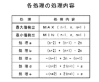
【0068】
処理回路159aにおける処理aでは、図4に示すように、n−2,n−1,nの画素データが使用され、(n−2)+(n−1)−2nの演算が行われることで、一の側の平坦度を示す信号が得られる。処理回路159cにおける処理bでは、図4に示すように、n+2,n+1,nの画素データが使用され、(n+2)+(n+1)−2nの演算が行われることで、他の側の平坦度を示す信号が得られる。
【0069】
図5は非線形特性回路159fにおける非線形特性の一例を示している。これにより、波形の平坦度を示す信号S1は0〜100の範囲に制限されて得られる。なお、画素データは例えば8ビットの信号であって、0〜255のレベルを持っているものとする。
【0070】
この第1の処理部159で得られる、注目位置の波形の平坦度を示す信号S1は、画像信号V2のエッジ部分近くの平坦な部分では小さな値となる。これにより、このエッジ部分近くの平坦な部分では波形の複雑さの度合いが低い、と判別されるようになる。
【0071】
また、波形判別部158は、注目位置における高域成分S2を得るための処理Bを行う第2の処理部160を備えている。この第2の処理部160は、注目位置における高域成分を抽出する処理cを行う処理回路160aと、この処理回路160aで得られる高域成分の絶対値をとる絶対値回路160bと、この絶対値回路160bの出力信号に非線形特性を付与して、上述した注目位置における高域成分S2とする非線形特性回路160cとからなっている。
【0072】
処理回路160aにおける処理cでは、図4に示すように、n−1,n,n+1の画素データが使用され、−(n−1)+2n−(n+1)の演算が行われることで、注目位置の高域成分が抽出される。非線形回路160cにおける非線形特性も、上述した非線形特性回路159fにおける非線形特性(図5参照)と同様であり、高域成分S2は0〜100の範囲に制限されて得られる。
【0073】
また、波形判別部158は、注目位置の両側における高域成分S3を得るための処理Cを行う第3の処理部161を備えている。この第3の処理部161は、注目位置に対して一の側の高域成分を抽出する処理dを行う処理回路161aと、この処理回路161aで抽出される高域成分の絶対値をとる絶対値回路161bと、注目位置に対して他の側の高域成分を抽出する処理eを行う処理回路161cと、この処理回路161cで抽出される高域成分の絶対値をとる絶対値回路161dと、絶対値回路161b,161dの出力信号の最小値を取り出す最小値回路161eと、この最小値回路161eの出力信号に非線形特性を付与して、上述した注目位置の両側における高域成分S3とする非線形特性回路161fとからなっている。
【0074】
処理回路161aにおける処理dでは、図4に示すように、n−2,n−1,nの画素データが使用され、−(n−2)+2(n−1)−nの演算が行われることで、一の側の高域成分が抽出される。処理回路161cにおける処理eでは、図4に示すように、n+2,n+1,nの画素データが使用され、−(n+2)+2(n+1)−nの演算が行われることで、他の側の高域成分が抽出される。非線形特性回路161fにおける非線形特性も、上述した非線形特性回路159fにおける非線形特性(図5参照)と同様であり、高域成分S3は0〜100の範囲に制限されて得られる。
【0075】
また、波形判別部158は、第1の処理部159で得られる注目位置の平坦度を示す信号S1に、第2の処理部160で得られる注目位置の高域成分S2を加算する加算器162と、この加算器162の出力信号から第3の処理部161で得られる注目位置の両側における高域成分S3を差し引く減算器163と、この減算器163の出力信号の最大値を100に制限して判別結果αを得るリミッタ164とを有している。
【0076】
また、エッジ改善部150は、上述した波形判別部158で得られる判別結果αまたは100の値の信号を選択的に取り出すスイッチ回路165を有している。スイッチ回路165のa側の固定端子には判別結果αが供給され、そのb側の固定端子には100の値の信号が供給される。このスイッチ回路165は、上述した振幅比較回路156で発生される切り換え制御信号SW2に基づいて、その接続が制御される。スイッチ回路165は、SW2=「1」のときはa側に接続され、一方SW2=「0」のときはb側に接続される。
【0077】
また、エッジ改善部150は、スイッチ回路165で取り出される信号mに基づいて、入力端子151に入力される画像信号V1の注目位置の画素データとスイッチ回路157で取り出される信号S4(最大値MAXまたは最小値MIN)とを混合し、画像信号V3の画素データを得る、信号抑圧手段を構成する混合回路166を有している。
【0078】
混合回路166では、画像信号V1の注目位置の画素データの値をx、信号S4の値をy、さらに画像信号V3の画素データの値をzとするとき、(1)式のように、混合が行われる。
z=x・m/100+y×(1−m/100) ・・・(1)
【0079】
図2に示すエッジ改善部150の動作を説明する。
入力端子151には、エンハンス処理された画像信号V1が入力される。この画像信号V1は、振幅比較回路156および混合回路166に供給される。また、入力端子152には、エンハンス処理されていない画像信号V2が入力される。この画像信号V2は、最大値検出回路154、最小値検出回路155および波形判別部158に供給される。
【0080】
最大値検出回路154では、画像信号V1の注目位置の近傍に位置する、画像信号V2の複数の画素データの最大値MAXが検出される。また、最小値検出回路155では、画像信号V1の注目位置の近傍に位置する、画像信号V2の複数の画素データの最小値MINが検出される。これら最大値MAXおよび最小値MINは振幅比較回路156に供給される。
【0081】
この最大値MAXおよび最小値MINの検出処理、さらには波形判別のための処理a〜eに使用する、画像信号V2の複数の画素データとしては、垂直エッジ改善部124の場合には垂直方向に並ぶ画素データが使用され、水平エッジ改善部129の場合には水平方向に並ぶ画素データが使用される。
【0082】
振幅比較回路156では、画像信号V1における注目位置の画素データの値xと、最大値MAXおよび最小値MINとが比較され、切り換え制御信号SW1,SW2が発生される。この場合、切り換え制御信号SW1は、x>MAXであるときは「1」となり、x<MINであるときは「0」となる。切り換え制御信号SW2は、x>MAXまたはx<MINであるときは「1」となり、MIN≦x≦MAXであるときは「0」となる。
【0083】
また、最大値検出回路154で検出される最大値MAXはスイッチ回路157のa側の固定端子に供給され、最小値検出回路155で検出される最小値MINはスイッチ回路157のb側の固定端子に供給される。このスイッチ回路157には、振幅比較回路156で発生される切り換え制御信号SW1が供給される。
【0084】
SW1=[1]であるとき、従ってx>MAXであるときは、スイッチ回路157はa側に接続され、スイッチ回路157の出力側に、最大値MAXが取り出される。一方、SW1=[0]であるとき、従ってx<MINであるときは、スイッチ回路157はb側に接続され、スイッチ回路157の出力側に、最小値MINが取り出される。このようにスイッチ回路157で取り出される信号S4、すなわち最大値MAXまたは最小値MINは混合回路166に供給される。
【0085】
また、波形判別部158では、画像信号V1における注目位置の近傍に位置する、画像信号V2の複数の画素データに基づいて、波形の複雑さの度合いが判別され、判別結果αが得られる。この判別結果αは、波形の複雑さの度合いが低い程小さくなる。
【0086】
この判別結果αは以下のようにして得られる。すなわち、第1の処理部159では、画像信号V1における注目位置の近傍に位置する、画像信号V2の複数の画素データに基づいて、注目位置の波形の平坦度を示す信号S1が得られる。この信号S1は、波形の複雑さの度合いが低い部分、例えば画像信号V2のエッジ部分近くの平坦な部分では小さな値となる。この信号S1が加算器162に供給される。
【0087】
また、第2の処理部160では、画像信号V1における注目位置の近傍に位置する、画像信号V2の複数の画素データに基づいて、注目位置における高域成分S2が得られる。この高域成分S2は加算器162に供給される。そして、加算器162では、信号S1に高域成分S2が加算される。この加算信号は減算器163に供給される。
【0088】
この場合、高域成分S2は、信号S1を補完するための信号として使用されている。すなわち、第1の処理部159で得られる信号S1は、波形が複雑な場合であっても、波形によっては、小さな値となることがある。その場合、高域成分S2の値は大きくなるので、信号S1を補完することができる。
【0089】
また、第3の処理部161では、画像信号V1における注目位置の近傍に位置する、画像信号V2の複数の画素データに基づいて、注目位置の両側における高域成分S3が得られる。この高域成分S3は減算器163に供給される。減算器163では、信号S1および高域成分S2の加算信号から高域成分S3が減算される。この場合、高域成分S3は、高域成分S2のレベルを抑えるために使用されている。これにより、高域成分S2を信号S1の補完信号として用いたことによる悪影響が軽減される。
【0090】
この減算器163の出力信号はリミッタ164に供給され、その最大値が100に制限される。このリミッタ164の出力信号が、波形判別部158における判別結果αとされる。
【0091】
波形判別部158で得られる判別結果αはスイッチ回路165のa側の固定端子に供給される。このスイッチ回路165のb側の固定端子には100の値の信号が供給される。このスイッチ回路165には、振幅比較回路156で発生される切り換え制御信号SW2が供給される。
【0092】
SW2=[1]であるとき、従ってx>MAXまたはx<MINであるときは、スイッチ回路165はa側に接続され、スイッチ回路165の出力信号mとして判別結果αが取り出される。一方、SW2=[0]であるとき、従ってMIN≦x≦MAXであるときは、スイッチ回路165はb側に接続され、スイッチ回路165の出力信号mとして100の値の信号が取り出される。
【0093】
このスイッチ回路165の出力信号mは、混合回路166に混合比率情報として供給される。混合回路166では、信号mに基づいて、(1)式によって、画像信号V3の画素データの値zが求められる。
【0094】
ここで、画像信号V1における注目位置の画素データの値xが最大値MAXより大きい場合(x>MAX)を考える。この場合、スイッチ回路157の出力信号S4は最大値MAXとなり、またスイッチ回路165の出力信号mは波形判別部158で得られる判別結果αとなる。
【0095】
そのため、混合回路166では、画像信号V1における注目位置の画素データの値xおよび最大値MAXが判別結果αに応じた比率で混合されて、画像信号V3の画素データの値zが生成される。この場合、波形の複雑さの度合いが低い程、判別結果αは小さくなるので、混合回路166で生成される画像信号V3の画素データの値zは、画像信号V1における注目位置の画素データの値xが最大値MAXに近づくように抑圧されたものとなる。
【0096】
また、画像信号V1における注目位置の画素データの値xが最小値MINより小さい場合(x<MIN)を考える。この場合、スイッチ回路157の出力信号S4は最小値MINとなり、またスイッチ回路165の出力信号mは波形判別部158で得られる判別結果αとなる。
【0097】
そのため、混合回路166では、画像信号V1における注目位置の画素データの値xおよび最小値MINが判別結果αに応じた比率で混合されて、画像信号V3の画素データの値zが生成される。この場合、波形の複雑さの度合いが低い程、判別結果αは小さくなるので、混合回路166で生成される画像信号V3の画素データの値zは、画像信号V1における注目位置の画素データの値xが最小値MINに近づくように抑圧されたものとなる。
【0098】
また、画像信号V1における注目位置の画素データの値xが最大値MAXから最小値MINまでの範囲にある場合(MIN≦x≦MAX)を考える。この場合、スイッチ回路165の出力信号mは100の値の信号となる。そのため、混合回路166では、画像信号V1における注目位置の画素データの値xがそのまま画像信号V3の画素データの値zとなる。
【0099】
このように図2に示すエッジ改善部150においては、エンハンス処理された画像信号V1における注目位置の画素データの値xが、エンハンス処理されていない画像信号V2の当該注目位置の近傍の画素データの最大値MAXより大きいとき、またはその最小値MINより小さいとき、画像信号V1における注目位置の画素データの値xが、当該注目位置の近傍の波形の複雑さの度合いが低い程最大値MAXまたは最小値MINに近づくように抑圧されて、出力画像信号V3が得られる。
【0100】
そして、波形判別部158では、例えば画像信号V2のエッジ部分近くの平坦な部分では波形の複雑さの度合いが低いと判別され、判別結果αは小さな値となる。この場合、混合回路166における抑圧度は大きく、出力端子153に出力される画像信号V3は、画像信号V1のエッジ部分近くの平坦な部分のレベル変化が大きく抑圧されたものとなる。例えば、画像信号V1が図20Bに示すようにそのエッジ部分近くの平坦な部分がレベル変化したものである場合、画像信号V3は図20Dに示すようにそのレベル変化が抑圧されたものとなる。この図20Dは、図20Cに示す理想的な場合と略等しい。これにより、画像信号V3による画像は、エッジ部分の両側に縁取りが目立たないものとなり、画質が向上する。
【0101】
波形の複雑さの度合いが高いと判断される場合には、判別結果αは大きくなる。この場合、混合回路166における抑圧度は小さく、出力端子153に出力される画像信号V3の画素データは、画像信号V1の画素データと略同じのものとなる。例えば、画像信号V1が図21Bに示すように平坦な部分のない信号であるとき、画像信号V3として図21Dに示すように画像信号V1とほとんど変わらないものを得ることができる。この図21Dは、図21Cに示す理想的な場合と略等しい。そのため、エンハンス処理による輪郭強調効果が弱められることはない。
【0102】
なお、エッジ部分そのものにおいても、波形の複雑さの度合いが高いと判断され、判別結果αが大きくなる。そのため、画像信号V3のエッジ部分は、画像信号V1のエッジ部分と同様に、エンハンス処理によって急峻にされた状態におかれる。つまり、エンハンス処理による輪郭強調効果が弱められることはない。
【0103】
また、図2に示すエッジ改善部150においては、波形判別部158で判別結果αを得る際に、主として、第1の処理部159で得られる注目位置の波形の平坦度を示す信号S1が用いられる。この信号S1は、波形が複雑な場合であっても、波形によっては、小さな値となることがある。そのため、この信号S1を補完するために、第2の処理部160で得られる高域成分S2が用いられている。したがって、波形が複雑な場合に、判別結果αが小さくなって、エンハンス処理による輪郭強調効果が弱められてしまうということを防止できる。
【0104】
なお、第2の処理部160における処理回路160aは3タップのハイパスフィルタを構成するものであって、タップ数が少ないため、高域成分S2の低域側のレベルの持ち上がりが少なく、この高域成分S2を信号S1の補完信号として使用しても、これによって、画像に目立つ縁取りが発生することはない。
【0105】
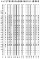
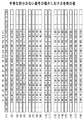
ここで、図2のエッジ改善部150における、(1)〜(18)の各部の実際の値の例を示す。この場合、エンハンス処理におけるハイパスフィルタ(垂直ハイパスフィルタ120または水平ハイパスフィルタ125)は11タップのものであり、その係数値は図6に示す通りであるとする。またこの場合、エンハンス処理における非線形特性回路(非線形特性回路121または非線形特性回路126)の非線形特性はオフ状態、つまり線形であるとする。また、非線形特性回路159f,160c,161fの非線形特性は、図5に示す通りとする。また、各値は、小数点以下を四捨五入したものとする。
【0106】
図7は、エッジと平坦な部分のある信号の場合(図20参照)における各部の値の例を示している。図8は、平坦な部分のない信号の場合(図21参照)における各部の値の例を示している。
【0107】
なお、(1)は入力端子152に入力される画像信号V2、(2)は入力端子151に入力される画像信号V1、(3)は最大値検出回路154で検出される最大値MAX,(4)は最小値検出回路155で検出される最小値MIN、(5)はスイッチ回路157の出力信号S4、(6)は第1の処理部159の絶対値回路159bの出力信号、(7)は第1の処理部159の絶対値回路159dの出力信号、(8)は第1の処理部159の最小値回路159eの出力信号、(9)は第1の処理部159の非線形特性回路159fの出力信号S1である。
【0108】
また、(10)は第2の処理部160の絶対値回路160bの出力信号、(11)は第2の処理部160の非線形特性回路160cの出力信号S2、(12)は第3の処理部161の絶対値回路161bの出力信号、(13)は第3の処理部161の絶対値回路161dの出力信号、(14)は第3の処理部161の最小値回路161eの出力信号、(15)は第3の処理部161の非線形特性回路161fの出力信号S3、(16)はリミッタ164の出力信号α、(17)はスイッチ回路165の出力信号m、(18)は混合回路166の出力信号、つまり出力端子153に出力される画像信号V3である。
【0109】
なお、図1の画像信号処理部102における処理を、例えば図9に示すような画像信号処理装置300によって、ソフトウェアで実現することも可能である。
【0110】
まず、図9に示す画像信号処理装置300について説明する。この画像信号処理装置300は、装置全体の動作を制御するCPU301と、このCPU301の動作プログラム等が格納されたROM(read only memory)302と、CPU301の作業領域を構成するRAM(random access memory)303とを有している。これらCPU301、ROM302およびRAM303は、それぞれバス304に接続されている。
【0111】
また、画像信号処理装置300は、外部記憶装置としてのハードディスクドライブ(HDD)305と、インターネット等の通信網400に有線または無線で接続する通信部308とを有している。これらHDD305および通信部308は、それぞれバス304に接続されている。
【0112】
また、画像信号処理装置300は、入力画像信号Vaを入力するための入力端子314と、出力画像信号Vbを出力するための出力端子315とを有している。これら入力端子314および出力端子315は、それぞれインタフェース316,317を介してバス304に接続される。
【0113】
ここで、入力画像信号Vaを入力端子314より入力する代わりに、予めHDD305に記録しておき、あるいはインターネットなどの通信網400より通信部308を介してダウンロードしてもよい。また、出力画像信号Voutを出力端子315に出力する代わり、あるいはそれと並行してHDD305に格納したり、通信部308を介してインターネットなどの通信網400に送出するようにしてもよい。
【0114】
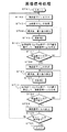
図10のフローチャートを参照して、図9に示す画像信号処理装置300における、入力画像信号Vaより出力画像信号Vbを得るための処理手順を説明する。
【0115】
まず、ステップST1で、処理を開始し、ステップST2で、入力画像信号Vaを1フレーム分入力する。この入力画像信号Vaが入力端子314より入力される場合には、この入力画像信号Vaを構成する画素データをRAM303に一時的に格納する。また、この入力画像信号VaがHDD305に記録されている場合には、HDD305から入力画像信号Vaを読み出し、この入力画像信号Vaを構成する画素データをRAM303に一時的に格納する。
【0116】
次に、ステップST3で、入力画像信号Vaより垂直方向の高域成分を抽出し、この高域成分を、非線形特性を付与した後に垂直輪郭信号として画像信号Vaに加算し、さらにこの加算信号の最大値を制限して、垂直方向の高域が強調された画像信号V12を生成する。
【0117】
次に、ステップST4では、画像信号V12における注目位置の垂直方向の波形の複雑さの度合いを判別して、判別結果αを求める。この判別は、画像信号V12における注目位置の近傍に位置する、画像信号Vaの垂直方向に並ぶ複数の画素データを使用して行われる。
【0118】
また、ステップST5で、画像信号V12における注目位置の近傍に位置する、画像信号Vaの垂直方向に並ぶ複数の画素データの最大値MAXおよび最小値MINを検出する。そして、ステップST6で、ステップST4で求められた判別結果αと、ステップST5で検出された最大値MAXおよび最小値MINとを用いて、画像信号V12における注目位置の画素データの値を抑圧して、画像信号V13を生成する。
【0119】
この場合、画像信号V12における注目位置の画素データの値xが、最大値MAXより大きいとき(x>MAX)、またはその最小値MINより小さいとき(x<MIN)、当該注目位置の近傍の波形の複雑さの度合いが低い程、つまり判別結果αが小さい程、画像信号V12における注目位置の画素データの値xを、最大値MAXまたは最小値MINに近づくように抑圧して、画像信号V13の画素データの値とする。
【0120】
なお、画像信号V12における注目位置の画素データの値xが最大値MAXから最小値MINまでの範囲にあるときは(MIN≦x≦MAX)、画像信号V12における注目位置の画素データの値xをそのまま画像信号V13の画素データの値とする。
【0121】
次に、ステップST7で、ステップST3で生成された画像信号V12の全ての画素データに対する処理が終了したか否かを判定する。終了していないときは、ステップST4に戻って、次の注目位置についての処理に移る。一方、終了したときは、ステップST8に進む。
【0122】
ステップST8では、画像信号V13より水平方向の高域成分を抽出し、この高域成分を、非線形特性を付与した後に水平輪郭信号として画像信号V13に加算し、さらにこの加算信号の最大値を制限して、垂直方向および水平方向の高域が強調された画像信号V15を生成する。
【0123】
次に、ステップST9では、画像信号V15における注目位置の水平方向の波形の複雑さの度合いを判別して、判別結果αを求める。この判別は、画像信号V15における注目位置の近傍に位置する、画像信号V13の水平方向に並ぶ複数の画素データを使用して行われる。
【0124】
また、ステップST10で、画像信号V15における注目位置の近傍に位置する、画像信号V13の水平方向に並ぶ複数の画素データの最大値MAXおよび最小値MINを検出する。そして、ステップST11で、ステップST9で求められた判別結果αと、ステップST10で検出された最大値MAXおよび最小値MINとを用いて、画像信号V15における注目位置の画素データの値を抑圧して、出力画像信号Vbを生成する。
【0125】
この場合、画像信号V15における注目位置の画素データの値xが、最大値MAXより大きいとき(x>MAX)、またはその最小値MINより小さいとき(x<MIN)、当該注目位置の近傍の水平方向の波形の複雑さの度合いが低い程、つまり判別結果αが小さい程、画像信号V15における注目位置の画素データの値xを、最大値MAXまたは最小値MINに近づくように抑圧して、画像信号Vbの画素データの値とする。
【0126】
なお、画像信号V15における注目位置の画素データの値xが最大値MAXから最小値MINまでの範囲にあるときは(MIN≦x≦MAX)、画像信号V15における注目位置の画素データの値xをそのまま画像信号Vbの画素データの値とする。
【0127】
次に、ステップST12で、ステップST8で生成された画像信号V15の全ての画素データに対する処理が終了したか否かを判定する。終了していないときは、ステップST9に戻って、次の注目位置についての処理に移る。一方、終了したときは、ステップST13に進む。
【0128】
ステップST13では、生成された1フレーム分の画像信号Vbを出力する。この場合、画像信号Vbを出力端子315に出力し、あるいはHDD305に供給して記録する。
【0129】
次に、ステップST14で、処理すべき全てのフレームの処理が終了したか否かを判定する。全フレームの処理が終了していないときは、ステップST2に戻り、次の1フレーム分の入力画像信号Vaの処理に移る。一方、全フレームの処理が終了したときは、ステップST15で、処理を終了する。
【0130】
このように、図10に示すフローチャートに沿って処理をすることで、図1の画像信号処理部102と同様に、入力された入力画像信号Vaの画素データを処理して、出力画像信号Vbの画素データを得ることができる。
【0131】
次に、この発明の第2の実施の形態について説明する。図11は、第2の実施の形態としての画像表示装置100Aの構成を示している。この図11において、図1と対応する部分には同一符号を付して示している。
【0132】
この画像表示装置100Aは、画像信号Vaが入力される入力端子101と、この画像信号Vaに対してエンハンス処理(輪郭強調処理)を行う画像信号処理部102Aと、LCD、PDP等で構成される表示素子104と、画像信号処理部102Aで得られる画像信号Vbに基づいて表示素子104を駆動し、この表示素子104の画面に画像信号Vbによる画像を表示するパネルドライバ103とを有している。
【0133】
図11に示す画像表示装置100Aの動作を説明する。
入力端子101には画像信号Vaが入力される。このように入力端子101に入力される画像信号Vaは画像信号処理部102Aに供給される。画像信号処理部102Aでは、画像信号Vaに対してエンハンス処理(輪郭強調処理)が行われる。この場合、画像信号Vaから例えば垂直方向および水平方向の高域成分が抽出され、この高域成分が画像信号Vaに加算されることで、高域の強調された画像信号Vbが得られる。画像信号処理部102Aで得られる画像信号Vbはパネルドライバ103に供給される。パネルドライバ103は、画像信号Vbに基づいて表示素子104を駆動し、表示素子104の画面に画像信号Vbによる画像を表示する。
【0134】
画像信号処理部102Aについてさらに説明する。
この画像信号処理部102Aは、入力端子101に入力される画像信号Vaを入力画像信号とし、この画像信号Vaから例えば垂直方向および水平方向の高域成分を輪郭信号として抽出する2次元ハイパスフィルタ(2次元HPF)130と、この輪郭信号に非線形特性を付与する非線形特性回路131とを有している。
【0135】
非線形特性回路131は、入力信号の絶対値レベルが所定値以下であるとき、出力信号のレベルを0とする。これにより、ノイズ成分が強調されることが防止される。また、非線形特性回路131は、入力信号の絶対値レベルが所定値以上であるとき、出力信号のレベルを一定値とする。これにより、高域の信号レベルが飽和することが防止される。
【0136】
また、画像信号処理部102Aは、画像信号Vaに非線形特性回路131で非線形特性が付与された輪郭信号を加算して、垂直方向および水平方向の高域が強調された画像信号V41を得る加算器132と、オーバフローおよびアンダーフローを防止するために、加算器132で得られる画像信号V21の振幅を制限するリミッタ133と、このリミッタ133から出力される画像信号V42における垂直方向および水平方向のエッジ部分近くの平坦な部分のレベル変化を抑圧する2次元エッジ改善部134とを有している。この2次元エッジ改善部134の具体的な構成については後述する。この2次元エッジ改善部134から出力される画像信号Vbが画像信号処理部102Aの出力画像信号となる。
【0137】
画像信号処理部102Aの動作を説明する。
入力画像信号としての画像信号Vaは2次元ハイパスフィルタ130に供給される。この2次元ハイパスフィルタ130では、画像信号Vaから垂直方向および水平方向の高域成分が輪郭信号として抽出される。この輪郭信号は非線形特性回路131を介して加算器132に供給される。
【0138】
この加算器132には、入力画像信号としての画像信号Vaも供給される。加算器122では、画像信号Vaに輪郭信号が加算され、垂直方向および水平方向の高域が強調された画像信号V41が得られる。この画像信号V41はリミッタ133に供給される。このリミッタ133では、画像信号V41の振幅が制限され、オーバフローおよびアンダーフローが防止される。
【0139】
また、リミッタ133から出力される画像信号V42は2次元エッジ改善部134に供給される。画像信号V42は上述したように画像信号Vaに垂直方向および水平方向の高域成分である輪郭信号が加算されて得られたものである。そのため、この画像信号V42における垂直方向および水平方向のエッジ部分近くの平坦な部分のレベルは変化したものとなっている(図20B参照)。したがって、この画像信号V42そのものによる画像を表示素子104に表示したとすれば、画像の垂直方向および水平方向のエッジ部分の両側に縁取りが発生し、エッジ部分の画質が劣化したものとなる。
【0140】
そのため、2次元エッジ改善部134では、画像信号V42における垂直方向および水平方向のエッジ部分近くの平坦な部分のレベル変化が抑圧される。これにより、画像の垂直方向および水平方向のエッジ部分の両側の縁取りは目立たなくなり、このエッジ部分の画質が改善される。
【0141】
次に、2次元エッジ改善部134の具体的な構成について説明する。図12は、エッジ改善部134の構成を示している。この図12において、図2と対応する部分には同一符号を付し、その詳細説明は省略する。
【0142】
このエッジ改善部134は、エンハンス処理された画像信号V42を入力する入力端子151と、エンハンス処理されていない画像信号Vaを入力する入力端子152と、画質改善後の画像信号Vbを出力する出力端子153とを有している。
【0143】
また、エッジ改善部134は、画像信号V42の注目位置の近傍に位置する、画像信号Vaの複数の画素データの最大値MAXを検出する最大値検出回路154Aと、画像信号V42の注目位置の近傍に位置する、画像信号Vaの複数の画素データの最小値MINを検出する最小値検出回路155Aとを有している。
【0144】
上述した図3は、最大値MAXおよび最小値MINの検出処理、波形判別のための処理a〜eに使用する、複数の画素データの一例を示すものであり、n−2〜n+2の画素データは垂直方向または水平方向に並ぶ画素データを示している。
【0145】
2次元エッジ改善部134では、垂直方向に並ぶn−2〜n+2の画素データおよび水平方向に並ぶn−2〜n+2の画素データが使用される。上述したように、nの画素データは注目位置に位置する画素データである。n−1,n−2の画素データは、nの画素データに対して、一側に位置しており、それぞれ1画素前、2画素前の画素データである。n+1,n+2の画素データは、nの画素データに対して、他側に位置しており、それぞれ1画素後、2画素後の画素データである。
【0146】
最大値検出回路154Aにおける最大値MAXの検出処理では、垂直方向のn−1,n,n+1の画素データおよび水平方向のn−1,n,n+1の画素データが使用され、それらの画素データの最大値が検出される。また、最小値検出回路155Aにおける最小値MINの検出処理では、垂直方向のn−1,n,n+1の画素データおよび水平方向のn−1,n,n+1の画素データが使用され、それらの画素データの最小値が検出される。
【0147】
また、エッジ改善部134は、画像信号V42の注目位置の画素データの値と、最大値検出回路154Aで検出された最大値MAXおよび最小値検出回路155Aで検出された最小値MINとを比較して、切り換え制御信号SW1,SW2を発生する振幅比較回路156を有している。
【0148】
振幅比較回路156は、画像信号V1の注目位置の画素データの値をxとし、x>MAXであるときは「1」となり、x<MINであるときは「0」となる切り換え制御信号SW1を発生する。また、振幅比較回路156は、x>MAXまたはx<MINであるときは「1」となり、MIN≦x≦MAXであるときは「0」となる切り換え制御信号SW2を発生する。
【0149】
また、エッジ改善部134は、上述した最大値MAXまたは最小値MINを選択的に取り出すスイッチ回路157を有している。スイッチ回路157のa側の固定端子には最大値検出回路154Aで検出された最大値MAXが供給され、そのb側の固定端子には最小値検出回路155Aで検出された最小値MINが供給される。このスイッチ回路157は、振幅比較回路156で発生される切り換え制御信号SW1に基づいて、その接続が制御される。スイッチ回路157は、SW1=「1」のときはa側に接続され、一方SW1=「0」のときはb側に接続される。
【0150】
また、エッジ改善部134は、画像信号V42における注目位置の近傍に位置する、画像信号Vaの複数の画素データに基づいて、波形の複雑さの度合いを判別する波形判別部158Aを有している。
【0151】
この波形判別部158Aは、注目位置の水平方向の波形の複雑さの度合いを示す信号Shを得るための水平処理部171Hと、注目位置の垂直方向の波形の複雑さの度合いを示す信号Svを得るための垂直処理部171Vと、これら信号Sh,Svを加算する加算器172と、この加算器172の出力信号の最大値を100に制限して判別結果αを得るリミッタ164とを備えている。処理部171H,171Vは、それぞれ、図2に示すエッジ改善部150の波形判別部158における処理部159〜161、加算器162および減算器163と同様に構成されている。
【0152】
この場合、水平処理部171Hでは、処理a、処理部b、処理c、処理dおよび処理eは、それぞれ、水平方向の、n−2,n−1,nの画素データ、n+2,n+1,nの画素データ、n−1,n,n+1の画素データ、n−2,n−1,nの画素データおよびn+2,n+1,nの画素データが使用されて行われる。一方、垂直処理部171Vでは、処理a、処理部b、処理c、処理dおよび処理eは、それぞれ、垂直方向の、n−2,n−1,nの画素データ、n+2,n+1,nの画素データ、n−1,n,n+1の画素データ、n−2,n−1,nの画素データおよびn+2,n+1,nの画素データが使用されて行われる。
【0153】
また、エッジ改善部134は、上述した波形判別部158Aで得られる判別結果αまたは100の値の信号を選択的に取り出すスイッチ回路165を有している。スイッチ回路165のa側の固定端子には判別結果αが供給され、そのb側の固定端子には100の値の信号が供給される。このスイッチ回路165は、上述した振幅比較回路156で発生される切り換え制御信号SW2に基づいて、その接続が制御される。スイッチ回路165は、SW2=「1」のときはa側に接続され、一方SW2=「0」のときはb側に接続される。
【0154】
また、エッジ改善部134は、スイッチ回路165で取り出される信号mに基づいて、入力端子151に入力される画像信号V42の注目位置の画素データとスイッチ回路157で取り出される信号S4(最大値MAXまたは最小値MIN)とを混合し、画像信号Vbの画素データを得る、信号抑圧手段を構成する混合回路166を有している。
【0155】
混合回路166では、画像信号V21の注目位置の画素データの値をx、信号S4の値をy、さらに画像信号Vbの画素データの値をzとするとき、上述した(1)式のように、混合が行われる。
【0156】
図12に示すエッジ改善部134の動作を説明する。
入力端子151には、エンハンス処理された画像信号V42が入力される。この画像信号V42は、振幅比較回路156および混合回路166に供給される。また、入力端子152には、エンハンス処理されていない画像信号Vaが入力される。この画像信号Vaは、最大値検出回路154A、最小値検出回路155Aおよび波形判別部158Aに供給される。
【0157】
最大値検出回路154Aでは、画像信号V42の注目位置の近傍に位置する、画像信号Vaの複数の画素データの最大値MAXが検出される。また、最小値検出回路155Aでは、画像信号V42の注目位置の近傍に位置する、画像信号Vaの複数の画素データの最小値MINが検出される。これら最大値MAXおよび最小値MINは振幅比較回路156に供給される。この最大値MAXおよび最小値MINの検出処理、さらには波形判別のための処理a〜eに使用する、画像信号Vaの複数の画素データとしては、垂直方向に並ぶ画素データおよび水平方向に並ぶ画素データが使用される。
【0158】
振幅比較回路156では、画像信号V1における注目位置の画素データの値xと、最大値MAXおよび最小値MINとが比較され、切り換え制御信号SW1,SW2が発生される。この場合、切り換え制御信号SW1は、x>MAXであるときは「1」となり、x<MINであるときは「0」となる。切り換え制御信号SW2は、x>MAXまたはx<MINであるときは「1」となり、MIN≦x≦MAXであるときは「0」となる。
【0159】
また、最大値検出回路154Aで検出される最大値MAXはスイッチ回路157のa側の固定端子に供給され、最小値検出回路155Aで検出される最小値MINはスイッチ回路157のb側の固定端子に供給される。このスイッチ回路157には、振幅比較回路156で発生される切り換え制御信号SW1が供給される。
【0160】
SW1=[1]であるとき、従ってx>MAXであるときは、スイッチ回路157はa側に接続され、スイッチ回路157の出力側に、最大値MAXが取り出される。一方、SW1=[0]であるとき、従ってx<MINであるときは、スイッチ回路157はb側に接続され、スイッチ回路157の出力側に、最小値MINが取り出される。このようにスイッチ回路157で取り出される信号S4、すなわち最大値MAXまたは最小値MINは混合回路166に供給される。
【0161】
また、波形判別部158Aでは、画像信号V42における注目位置の近傍に位置する、画像信号Vaの複数の画素データに基づいて、水平方向および垂直方向の波形の複雑さの度合いが判別され、判別結果αが得られる。この判別結果αは、波形の複雑さの度合いが低い程小さくなる。この判別結果αは、水平処理部171Hで生成される水平方向の波形の複雑さを示す信号Shと垂直処理部171Vで生成される垂直方向の波形の複雑さを示す信号Svとが加算器172で加算され、さらにその加算信号がリミッタ164で最大値が100に制限されて得られる。
【0162】
波形判別部158Aで得られる判別結果αはスイッチ回路165のa側の固定端子に供給される。このスイッチ回路165のb側の固定端子には100の値の信号が供給される。このスイッチ回路165には、振幅比較回路156で発生される切り換え制御信号SW2が供給される。
【0163】
SW2=[1]であるとき、従ってx>MAXまたはx<MINであるときは、スイッチ回路165はa側に接続され、スイッチ回路165の出力信号mとして判別結果αが取り出される。一方、SW2=[0]であるとき、従ってMIN≦x≦MAXであるときは、スイッチ回路165はb側に接続され、スイッチ回路165の出力信号mとして100の値の信号が取り出される。
【0164】
このスイッチ回路165の出力信号mは、混合回路166に混合比率情報として供給される。混合回路166では、信号mに基づいて、(1)式によって、画像信号Vbの画素データの値zが求められる。
【0165】
ここで、画像信号V42における注目位置の画素データの値xが最大値MAXより大きい場合(x>MAX)を考える。この場合、スイッチ回路157の出力信号S4は最大値MAXとなり、またスイッチ回路165の出力信号mは波形判別部158Aで得られる判別結果αとなる。
【0166】
そのため、混合回路166では、画像信号V42における注目位置の画素データの値xおよび最大値MAXが判別結果αに応じた比率で混合されて、画像信号Vbの画素データの値zが生成される。この場合、波形の複雑さの度合いが低い程、判別結果αは小さくなるので、混合回路166で生成される画像信号Vbの画素データの値zは、画像信号V42における注目位置の画素データの値xが最大値MAXに近づくように抑圧されたものとなる。
【0167】
また、画像信号V42における注目位置の画素データの値xが最小値MINより小さい場合(x<MIN)を考える。この場合、スイッチ回路157の出力信号S4は最小値MINとなり、またスイッチ回路165の出力信号mは波形判別部158Aで得られる判別結果αとなる。
【0168】
そのため、混合回路166では、画像信号V42における注目位置の画素データの値xおよび最大値MAXが判別結果αに応じた比率で混合されて、画像信号V3の画素データの値zが生成される。この場合、波形の複雑さの度合いが低い程、判別結果αは小さくなるので、混合回路166で生成される画像信号Vbの画素データの値zは、画像信号V42における注目位置の画素データの値xが最小値MINに近づくように抑圧されたものとなる。
【0169】
また、画像信号V42における注目位置の画素データの値xが最大値MAXから最小値MINまでの範囲にある場合(MIN≦x≦MAX)を考える。この場合、スイッチ回路165の出力信号mは100の値の信号となる。そのため、混合回路166では、画像信号V42における注目位置の画素データの値xがそのまま画像信号Vbの画素データの値zとなる。
【0170】
このように図12に示す2次元エッジ改善部134は、図2に示すエッジ改善部150と同様の動作をするので、エッジ改善部150と同様の作用効果を得ることができる。
【0171】
なお、図11の画像信号処理部102Aにおける処理を、例えば図9に示すような画像信号処理装置300によって、ソフトウェアで実現することも可能である。
【0172】
図13のフローチャートを参照して、図9に示す画像信号処理装置300における、入力画像信号Vaより出力画像信号Vbを得るための処理手順を説明する。
【0173】
まず、ステップST21で、処理を開始し、ステップST22で、入力画像信号Vaを1フレーム分入力する。この入力画像信号Vaが入力端子314より入力される場合には、この入力画像信号Vaを構成する画素データをRAM303に一時的に格納する。また、この入力画像信号VaがHDD305に記録されている場合には、HDD305から入力画像信号Vaを読み出し、この入力画像信号Vaを構成する画素データをRAM303に一時的に格納する。
【0174】
次に、ステップST23で、入力画像信号Vaより垂直方向および水平方向の高域成分を抽出し、この高域成分を、非線形特性を付与した後に垂直および水平の輪郭信号として画像信号Vaに加算し、さらにこの加算信号の最大値を制限して、垂直方向および水平方向の高域が強調された画像信号V42を生成する。
【0175】
次に、ステップST24では、画像信号V42における注目位置の垂直方向および水平方向の波形の複雑さの度合いを判別して、判別結果αを求める。この判別は、画像信号V42における注目位置の近傍に位置する、画像信号Vaの垂直方向および水平方向に並ぶ複数の画素データを使用して行われる。
【0176】
次に、ステップST25で、画像信号V42における注目位置の近傍に位置する、画像信号Vaの垂直方向および水平方向に並ぶ複数の画素データの最大値MAXおよび最小値MINを検出する。そして、ステップST26で、ステップST24で求められた判別結果αと、ステップST25で検出された最大値MAXおよび最小値MINとを用いて、画像信号V42における注目位置の画素データの値を抑圧して、画像信号Vbを生成する。
【0177】
この場合、画像信号Vbにおける注目位置の画素データの値xが、最大値MAXより大きいとき(x>MAX)、またはその最小値MINより小さいとき(x<MIN)、当該注目位置の近傍の波形の複雑さの度合いが低い程、つまり判別結果αが小さい程、画像信号V42における注目位置の画素データの値xを、最大値MAXまたは最小値MINに近づくように抑圧して、画像信号Vbの画素データの値とする。
【0178】
なお、画像信号V42における注目位置の画素データの値xが最大値MAXから最小値MINまでの範囲にあるときは(MIN≦x≦MAX)、画像信号V42における注目位置の画素データの値xをそのまま画像信号Vbの画素データの値とする。
【0179】
次に、ステップST27で、ステップST23で生成された画像信号V42の全ての画素データに対する処理が終了したか否かを判定する。終了していないときは、ステップST24に戻って、次の注目位置についての処理に移る。一方、終了したときは、ステップST28に進む。
【0180】
ステップST28では、生成された1フレーム分の画像信号Vbを出力する。この場合、画像信号Vbを出力端子315に出力し、あるいはHDD305に供給して記録する。
【0181】
次に、ステップST29で、処理すべき全てのフレームの処理が終了したか否かを判定する。全フレームの処理が終了していないときは、ステップST22に戻り、次の1フレーム分の入力画像信号Vaの処理に移る。一方、全フレームの処理が終了したときは、ステップST30で、処理を終了する。
【0182】
このように、図13に示すフローチャートに沿って処理をすることで、図11に示す画像信号処理部102Aと同様に、入力された入力画像信号Vaの画素データを処理して、出力画像信号Vbの画素データを得ることができる。
【0183】
なお、図11の画像信号処理部102Aにおいては、2次元ハイパスフィルタ130で画像信号Vaの垂直方向および水平方向の高域成分を抽出し、これを輪郭信号として画像信号Vaに加算するものである。しかし、このハイパスフィルタ130で、さらに第1の斜め方向(右上がり方向)および第2の斜め方向(右下がり方向)の高域成分を抽出し、これをも輪郭信号として画像信号Vaに加算することも考えられる。これにより、斜め方向の輪郭が強調されて、鮮鋭感が増すようになる。
【0184】
しかしこの場合、斜め方向に関して、上述した垂直方向および水平方向と同様に、エッジ部分近くの平坦な部分のレベルが変化し、このレベル変化のために画像のエッジ部分の両側に縁取りが発生する。
【0185】
したがってこの場合には、斜め方向に関しても、上述した垂直方向および水平方向と同様に、画像信号のエッジ部分近くの平坦な部分のレベル変化を抑圧し、画像のエッジ部分の両側の縁取りが目立つことを軽減する必要がある。
【0186】
そこで、上述したように画像信号Vaに斜め方向の高域成分をも加算して、斜め方向の輪郭を強調する場合には、図12に示す2次元エッジ改善部134を、例えば以下のように変更すればよい。
【0187】
すなわち、最大値検出回路154Aは、画像信号V42の注目位置の近傍に位置する、画像信号Vaの垂直方向、水平方向、第1の斜め方向さらには第2の斜め方向に並ぶ複数の画素データを使用し、これらの画素データの最大値MAXを検出するようにされる。
【0188】
同様に、最小値検出回路155Aは、画像信号V42の注目位置の近傍に位置する、画像信号Vaの垂直方向、水平方向、第1の斜め方向さらには第2の斜め方向に並ぶ複数の画素データを使用し、これらの画素データの最小値MINを検出するようにされる。
【0189】
また、波形判別部158Aは、注目位置の水平方向の波形の複雑さの度合いを示す信号Shを得るための水平処理部171Hおよび注目位置の垂直方向の波形の複雑さの度合いを示す信号Svを得るための垂直処理部171Vの他に、破線図示するように、注目位置の第1の斜め方向の波形の複雑さの度合いを示す信号Sb1を得るための斜め処理部171B1および注目位置の第2の斜め方向の波形の複雑さの度合いを示す信号Sb2を得るための斜め処理部171B2を備えるようにされる。
【0190】
これら斜め処理部171B1,171B2は、水平処理部171H、垂直処理部171Vと同様に構成される。ただし、斜め処理部171B1では、注目位置の近傍に位置する、画像信号Vaの第1の斜め方向に並ぶ複数の画素データを使用して処理a〜eが行われる。また、斜め処理部171B2では、注目位置の近傍に位置する、画像信号Vaの第2の斜め方向に並ぶ複数の画素データを使用して処理a〜eが行われる。
【0191】
波形判別部158Aでは、加算器172で信号Sh,Svの他に、信号Sb1,Sb2も加算され、さらにこの加算信号がリミッタ164で最大値が100に制限されて判別結果αとなるようにされる。
【0192】
次に、この発明の第3の実施の形態について説明する。図14は、第3の実施の形態としての画像表示装置100Bの構成を示している。この図14において、図1と対応する部分には同一符号を付して示している。
【0193】
この画像表示装置100Bは、画像信号Vaが入力される入力端子101と、この画像信号Vaに対してスケーリング処理(画素数変換処理)を行う画像信号処理部102Bと、LCD、PDP等で構成される表示素子104と、画像信号処理部102Bで得られる画像信号Vbに基づいて表示素子104を駆動し、この表示素子104の画面に画像信号Vbによる画像を表示するパネルドライバ103とを有している。
【0194】
図14に示す画像表示装置100Bの動作を説明する。
入力端子101には画像信号Vaが入力される。このように入力端子101に入力される画像信号Vaは画像信号処理部102Bに供給される。画像信号処理部102Bでは、画像信号Vaに対してスケーリング処理(画素数変換処理)が行われる。この場合、画像信号Vaに基づいて、水平方向および垂直方向の補間位置の画素データが生成されることで、これら水平方向および垂直方向の画素数が変換される。この補間は、従来周知の線形補間、キュービック補間、最近傍補間等の手法によって行われる。画像信号処理部102Bで得られる画像信号Vbはパネルドライバ103に供給される。パネルドライバ103は、画像信号Vbに基づいて表示素子104を駆動し、表示素子104の画面に画像信号Vbによる画像を表示する。
【0195】
画像信号処理部102Bについてさらに説明する。
この画像信号処理部102Bは、入力端子101に入力される画像信号Vaを入力画像信号とし、この画像信号Vaに基づいて、垂直方向の補間位置の画素データを生成し、画像信号V31を得る垂直補間回路140を有している。この場合、画像信号V31における注目位置の画素データは、この注目位置の近傍に位置する画像信号Vaの複数の画素データを用いて生成される。
【0196】
また、この画像信号処理部102Bは、垂直補間回路140より出力される画像信号V31における垂直方向のエッジ部分近くの平坦な部分に発生するリンギング(レベル変化)を抑圧する垂直エッジ改善部141を有している。この垂直エッジ改善部141の具体的な構成については後述する。
【0197】
また、画像信号処理部102Bは、垂直エッジ改善部141より出力される画像信号V32に基づいて、水平方向の補間位置の画素データを生成し、画像信号V33を得る水平補間回路142を有している。この場合、画像信号V33における注目位置の画素データは、この注目位置の近傍に位置する画像信号V32の複数の画素データを用いて生成される。
【0198】
また、この画像信号処理部102Bは、水平補間回路142より出力される画像信号V33における水平方向のエッジ部分近くの平坦な部分に発生するリンギング(レベル変化)を抑圧する水平エッジ改善部143を有している。この水平エッジ改善部143の具体的な構成については後述する。この水平エッジ改善部143から出力される画像信号Vbが画像信号処理部102Bの出力画像信号となる。
【0199】
画像信号処理部102Bの動作を説明する。
入力画像信号としての画像信号Vaは垂直補間回路140に供給される。この垂直補間回路140では、画像信号Vaに基づいて、垂直方向の補間位置の画素データが生成され、垂直方向の画素数が、例えば増加する方向に変換される。
【0200】
垂直補間回路140より出力される画像信号V31は垂直エッジ改善部141に供給される。画像信号V31は上述したように補間処理によって垂直方向の画素数が変換されたものである。そのため、この画像信号V31の垂直方向のエッジ部分近くの平坦な部分にはリンギング(レベル変化)が発生している。したがって、この画像信号V31そのものによる画像を表示素子104に表示したとすれば、画像の垂直方向のエッジ部分の画質が劣化したものとなる。
【0201】
そのため、垂直エッジ改善部141では、画像信号V31における垂直方向のエッジ部分近くの平坦な部分のリンギング(レベル変化)が抑圧される。これにより、画像の垂直方向のエッジ部分の画質劣化が改善される。
【0202】
また、垂直エッジ改善部141より出力される画像信号V32は水平補間回路142に供給される。この水平補間回路142では、画像信号V32に基づいて、水平方向の補間位置の画素データが生成され、水平方向の画素数が、例えば増加する方向に変換される。
【0203】
水平補間回路142より出力される画像信号V33は水平エッジ改善部143に供給される。画像信号V33は上述したように補間処理によって水平方向の画素数が変換されたものである。そのため、この画像信号V33の水平方向のエッジ部分近くの平坦な部分にはリンギング(レベル変化)が発生している。したがって、この画像信号V33そのものによる画像を表示素子104に表示したとすれば、画像の水平方向のエッジ部分の画質が劣化したものとなる。
【0204】
そのため、水平エッジ改善部143では、画像信号V33における水平方向のエッジ部分近くの平坦な部分のリンギング(レベル変化)が抑圧される。これにより、画像の水平方向のエッジ部分の画質劣化が改善される。
【0205】
次に、エッジ改善部150B(垂直エッジ改善部141、水平エッジ改善部143)の具体的な構成について説明する。図15は、エッジ改善部150Bの構成を示している。この図15において、図2と対応する部分には同一符号を付し、その詳細説明は省略する。
【0206】
このエッジ改善部150Bは、スケーリング処理された画像信号V1を入力する入力端子151と、スケーリング処理されていない画像信号V2を入力する入力端子152と、画質改善後の画像信号V3を出力する出力端子153とを有している。ここで、画像信号V1は、垂直エッジ改善部141の場合には画像信号V31であり、水平エッジ改善部143の場合には画像信号V33である。画像信号V2は、垂直エッジ改善部141の場合には画像信号Vaであり、水平エッジ改善部143の場合には画像信号V32である。画像信号V3は、垂直エッジ改善部141の場合には画像信号V32であり、水平エッジ改善部143の場合には画像信号Vbである。
【0207】
また、エッジ改善部150Bは、画像信号V1における注目位置の近傍に位置する画像信号V2の所定方向に並ぶ複数、例えば2個の画素データについて、その画素データの近傍に位置する所定方向に並ぶ複数の画素データから最大値MAXを検出する最大値検出回路154Bと、その複数の画素データの最小値MINを検出する最小値検出回路155Bとを有している。この場合、垂直エッジ改善部141では上述の所定方向は垂直方向であり、水平エッジ改善部143では上述の所定方向は水平方向である。
【0208】
また、エッジ改善部150Bは、最大値検出回路154Bで検出される複数、例えば2個の最大値MAXから補間処理によって、画像信号V1における注目位置に対応した最大値MAXを得る補間回路181と、最小値検出回路155Bで検出される複数、例えば2個の最小値MINから補間処理によって、画像信号V1における注目位置に対応した最小値MINを得る補間回路182とを有している。これら補間回路181,182では、例えば、直線補間、最近傍補間等の補間処理が行われる。
【0209】
また、エッジ改善部150Bは、画像信号V1の注目位置の画素データの値と、補間回路181で得られた最大値MAXおよび補間回路182で得られた最小値MINとを比較して、切り換え制御信号SW1,SW2を発生する振幅比較回路156を有している。
【0210】
振幅比較回路156は、画像信号V1の注目位置の画素データの値をxとし、x>MAXであるときは「1」となり、x<MINであるときは「0」となる切り換え制御信号SW1を発生する。また、振幅比較回路156は、x>MAXまたはx<MINであるときは「1」となり、MIN≦x≦MAXであるときは「0」となる切り換え制御信号SW2を発生する。
【0211】
また、エッジ改善部150Bは、上述した最大値MAXまたは最小値MINを選択的に取り出すスイッチ回路157を有している。スイッチ回路157のa側の固定端子には補間回路181で得られた最大値MAXが供給され、そのb側の固定端子には補間回路182で得られた最小値MINが供給される。このスイッチ回路157は、振幅比較回路156で発生される切り換え制御信号SW1に基づいて、その接続が制御される。スイッチ回路157は、SW1=「1」のときはa側に接続され、一方SW1=「0」のときはb側に接続される。
【0212】
また、エッジ改善部150Bは、画像信号V1またはスイッチ回路157の出力信号S4を選択的に取り出すスイッチ回路183を有している。スイッチ回路183のa側の固定端子には画像信号V1が供給され、そのb側の固定端子には出力信号S4が供給される。このスイッチ回路183は、振幅比較回路156で発生される切り換え制御信号SW2に基づいて、その接続が制御される。スイッチ回路183は、SW2=「0」のときはa側に接続され、一方SW2=「1」のときはb側に接続される。
【0213】
また、エッジ改善部150Bは、画像信号V1における注目位置の近傍に位置する、スイッチ回路183の出力信号S5の複数の画素データに基づいて、波形の複雑さの度合いを判別する波形判別部158を有している。この波形判別部158は、波形判別のための画像信号が、画像信号V2ではなくスイッチ回路183の出力信号S5である他は、図2に示す波形判別部158と同じ構成である。
【0214】
このように画像信号V2を使用しないのは、この画像信号V2はスケーリング処理(画素数変換処理)を行う前のものであり、画像信号V1とは画素数が異なっており、画像信号V1の各画素データに対応した波形の判別結果αを得ることができないからである。なお、スイッチ回路183の出力信号S5の代わりに、スイッチ回路157の出力信号S4を使用することもできる。
【0215】
なお、垂直エッジ改善部141では、出力信号S5の垂直方向に並ぶ複数の画素データが使用されて、処理a〜eが行われる。また、水平エッジ改善部143では、出力信号S5の水平方向に並ぶ複数の画素データが使用されて、処理a〜eが行われる。
【0216】
また、エッジ改善部150Bは、波形判別部158で得られる判別結果αに基づいて、入力端子151に入力される画像信号V1の注目位置の画素データとスイッチ回路183で取り出される信号S5とを混合し、画像信号V3の画素データを得る、信号抑圧手段を構成する混合回路166を有している。
【0217】
混合回路166では、画像信号V1の注目位置の画素データの値をx、信号S5の値をy、さらに画像信号V3の画素データの値をzとするとき、(2)式のように、混合が行われる。
z=x・α/100+y×(1−α/100) ・・・(2)
【0218】
図15に示すエッジ改善部150Bの動作を説明する。
入力端子151には、スケーリング処理された画像信号V1が入力される。この画像信号V1は、振幅比較回路156、混合回路166およびスイッチ回路183のa側の固定端子に供給される。また、入力端子152には、スケーリング処理されていない画像信号V2が供給される。この画像信号V2は、最大値検出回路154Bおよび最小値検出回路155Bに供給される。
【0219】
最大値検出回路154Bでは、画像信号V1における注目位置の近傍に位置する画像信号V2の複数、例えば2個の画素データについて、その画素データの近傍に位置する複数の画素データから最大値MAXが検出される。この最大値検出回路154Bで検出される複数、例えば2個の最大値MAXは補間回路181に供給される。補間回路181では、この複数の最大値MAXから補間処理によって、画像信号V1における注目位置に対応した最大値MAXが得られる。
【0220】
また、最小値検出回路155Bでは、画像信号V1における注目位置の近傍に位置する画像信号V2の複数、例えば2個の画素データについて、その画素データの近傍に位置する複数の画素データから最小値MINが検出される。この最小値検出回路155Bで検出される複数、例えば2個の最小値MINは補間回路182に供給される。補間回路182では、この複数の最小値MINから補間処理によって、画像信号V1における注目位置に対応した最小値MINが得られる。
【0221】
この最大値MAXおよび最小値MINの検出処理、さらには波形判別のための処理a〜eに使用する、複数の画素データとしては、垂直エッジ改善部141の場合には垂直方向に並ぶ画素データが使用され、水平エッジ改善部143の場合には水平方向に並ぶ画素データが使用される。
【0222】
補間回路181,182で得られる最大値MAX、最小値MINは振幅比較回路156に供給される。振幅比較回路156では、画像信号V1における注目位置の画素データの値xと、最大値MAXおよび最小値MINとが比較され、切り換え制御信号SW1,SW2が発生される。この場合、切り換え制御信号SW1は、x>MAXであるときは「1」となり、x<MINであるときは「0」となる。切り換え制御信号SW2は、x>MAXまたはx<MINであるときは「1」となり、MIN≦x≦MAXであるときは「0」となる。
【0223】
また、補間回路181で得られる最大値MAXはスイッチ回路157のa側の固定端子に供給され、補間回路182で得られる最小値MINはスイッチ回路157のb側の固定端子に供給される。このスイッチ回路157には、振幅比較回路156で発生される切り換え制御信号SW1が供給される。
【0224】
SW1=[1]であるとき、従ってx>MAXであるときは、スイッチ回路157はa側に接続され、スイッチ回路157の出力側に、最大値MAXが取り出される。一方、SW1=[0]であるとき、従ってx<MINであるときは、スイッチ回路157はb側に接続され、スイッチ回路157の出力側に、最小値MINが取り出される。
【0225】
スイッチ回路157の出力信号S4、すなわち最大値MAXまたは最小値MINは、スイッチ回路183のb側の固定端子に供給される。このスイッチ回路183には、振幅比較回路156で発生される切り換え制御信号SW2が供給される。
【0226】
SW2=[1]であるとき、従ってx>MAXまたはx<MINであるときは、スイッチ回路83はb側に接続され、スイッチ回路183の出力信号S5としてスイッチ回路157の出力信号S4、すなわち最大値MAXまたは最小値MINが取り出される。一方、SW2=[0]であるとき、従ってMIN≦x≦MAXであるときは、スイッチ回路183はa側に接続され、スイッチ回路183の出力信号S5として画像信号V1が取り出される。
【0227】
スイッチ回路183の出力信号S5は混合回路183および波形判別部158に供給される。波形判別部158では、画像信号V1における注目位置の近傍に位置する、出力信号S5の複数の画素データに基づいて、波形の複雑さの度合いが判別され、判別結果αが得られる。この判別結果αは、波形の複雑さの度合いが低い程小さくなる。
【0228】
波形判別部158で得られる判別結果αは、混合回路166に混合比率情報として供給される。混合回路166では、判別結果αに基づいて、(2)式によって、画像信号V3の画素データの値zが求められる。
【0229】
ここで、画像信号V1における注目位置の画素データの値xが最大値MAXより大きい場合(x>MAX)を考える。この場合、スイッチ回路157の出力信号S4は最大値MAXとなり、またスイッチ回路183の出力信号S5はスイッチ回路157の出力信号S4、すなわち最大値MAXとなる。
【0230】
そのため、混合回路166では、画像信号V1における注目位置の画素データの値xおよび最大値MAXが判別結果αに応じた比率で混合されて、画像信号V3の画素データの値zが生成される。この場合、波形の複雑さの度合いが低い程、判別結果αは小さくなるので、混合回路166で生成される画像信号V3の画素データの値zは、画像信号V1における注目位置の画素データの値xが最大値MAXに近づくように抑圧されたものとなる。
【0231】
また、画像信号V1における注目位置の画素データの値xが最小値MINより小さい場合(x<MIN)を考える。この場合、スイッチ回路157の出力信号S4は最小値MINとなり、またスイッチ回路183の出力信号S5はスイッチ回路157の出力信号S4、すなわち最小値MINとなる。
【0232】
そのため、混合回路166では、画像信号V1における注目位置の画素データの値xおよび最小値MINが判別結果αに応じた比率で混合されて、画像信号V3の画素データの値zが生成される。この場合、波形の複雑さの度合いが低い程、判別結果αは小さくなるので、混合回路166で生成される画像信号V3の画素データの値zは、画像信号V1における注目位置の画素データの値xが最小値MINに近づくように抑圧されたものとなる。
【0233】
また、画像信号V1における注目位置の画素データの値xが最大値MAXから最小値MINまでの範囲にある場合(MIN≦x≦MAX)を考える。この場合、スイッチ回路183の出力信号S5は画像信号V1となる。そのため、混合回路166では、判別結果αの値に拘わらず、画像信号V1における注目位置の画素データの値xがそのまま画像信号V3の画素データの値zとなる。
【0234】
このように図15に示すエッジ改善部150Bにおいては、スケーリング処理された画像信号V1における注目位置の画素データの値xが、スケーリング処理されていない画像信号V2の当該注目位置の近傍の画素データの最大値MAXより大きいとき、またはその最小値MINより小さいとき、当該注目位置の近傍の波形の複雑さの度合いが低い程、画像信号V1における注目位置の画素データの値xが最大値MAXまたは最小値MINに近づくように抑圧されて、出力画像信号V3が得られる。
【0235】
そして、波形判別部158では、例えば画像信号V2のエッジ部分近くの平坦な部分では波形の複雑さの度合いが低いと判別され、判別結果αは小さな値となる。この場合、混合回路166における抑圧度は大きく、出力端子153に出力される画像信号V3は、画像信号V1のエッジ部分近くの平坦な部分のリンギング(レベル変化)が大きく抑圧されたものとなる。これにより、画像信号V3による画像は、エッジ部分の画質が向上したものとなる。
【0236】
なお、図14の画像信号処理部102Bにおける処理を、例えば図9に示すような画像信号処理装置300によって、ソフトウェアで実現することも可能である。
【0237】
図16のフローチャートを参照して、図9に示す画像信号処理装置300における、入力画像信号Vaより出力画像信号Vbを得るための処理手順を説明する。
【0238】
まず、ステップST41で、処理を開始し、ステップST42で、入力画像信号Vaを1フレーム分入力する。この入力画像信号Vaが入力端子314より入力される場合には、この入力画像信号Vaを構成する画素データをRAM303に一時的に格納する。また、この入力画像信号VaがHDD305に記録されている場合には、HDD305から入力画像信号Vaを読み出し、この入力画像信号Vaを構成する画素データをRAM303に一時的に格納する。
【0239】
次に、ステップST43で、画像信号Vaに基づいて、垂直方向の補間位置の画素データを生成して画素数を変換し、画像信号V31を生成する。そして、ステップST44で、画像信号V31における注目位置に対応した最大値MAXおよび最小値MINを検出する。
【0240】
この場合、画像信号V31における注目位置の近傍に位置する、画像信号Vaの垂直方向に並ぶ複数、例えば2個の画素データについて、その画素データの近傍に位置する垂直方向に並ぶ複数の画素データから最大値MAXおよび最小値MINを検出する。そして、検出された複数、例えば2個の最大値MAXから補間処理によって、画像信号V31における注目位置に対応した最大値MAXを求める。同様に、検出された複数、例えば2個の最小値MINから補間処理によって、画像信号V31における注目位置に対応した最小値MINを求める。
【0241】
次に、ステップST45で、画像信号V31における注目位置の垂直方向の波形の複雑さの度合いを判別して、判別結果αを求める。この判別は、画像信号V31における注目位置の近傍に位置する、当該画像信号V31の垂直方向に並ぶ複数の画素データに対応した最大値MAXまたは最小値MINを使用して行われる。この複数の最大値MAXまたは最小値MINは、ステップST44と同様の処理で得られる。
【0242】
この場合、画像信号V31における注目位置の画素データの値xが、その注目位置に対応した最大値MAXより大きいとき(x>MAX)、複数の最大値MAXが使用され、一方画像信号V31における注目位置の画素データの値xが、その注目位置に対応した最小値MINより小さいとき(x<MIN)、複数の最小値MINが使用される。
【0243】
次に、ステップST46で、ステップST44で検出された最大値MAXおよび最小値MINと、ステップST45で得られた判別結果αとを用いて、画像信号V31における注目位置の画素データの値を抑圧して、画像信号V32を生成する。
【0244】
この場合、画像信号V31における注目位置の画素データの値xが、最大値MAXより大きいとき(x>MAX)、またはその最小値MINより小さいとき(x<MIN)、当該注目位置の近傍の波形の複雑さの度合いが低い程、つまり判別結果αが小さい程、画像信号V31における注目位置の画素データの値xを、最大値MAXまたは最小値MINに近づくように抑圧して、画像信号V32の画素データの値とする。
【0245】
なお、画像信号V31における注目位置の画素データの値xが最大値MAXから最小値MINまでの範囲にあるときは(MIN≦x≦MAX)、画像信号V31における注目位置の画素データの値xをそのまま画像信号V32の画素データの値とする。
【0246】
次に、ステップST47で、ステップST43で生成された画像信号V31の全ての画素データに対する処理が終了したか否かを判定する。終了していないときは、ステップST44に戻って、次の注目位置についての処理に移る。一方、終了したときは、ステップST48に進む。
【0247】
ステップST48では、画像信号V32に基づいて、水平方向の補間位置の画素データを生成して画素数を変換し、画像信号V33を生成する。そして、ステップST49で、画像信号V33における注目位置に対応した最大値MAXおよび最小値MINを検出する。
【0248】
この場合、画像信号V33における注目位置の近傍に位置する画像信号V32の水平方向に並ぶ複数、例えば2個の画素データについて、その画素データの近傍に位置する水平方向に並ぶ複数の画素データから最大値MAXおよび最小値MINを検出する。そして、検出された複数、例えば2個の最大値MAXから補間処理によって、画像信号V33における注目位置に対応した最大値MAXを求める。同様に、検出された複数、例えば2個の最小値MINから補間処理によって、画像信号V33における注目位置に対応した最小値MINを求める。
【0249】
次に、ステップST50で、画像信号V33における注目位置の水平方向の波形の複雑さの度合いを判別して、判別結果αを求める。この判別は、画像信号V33における注目位置の近傍に位置する、当該画像信号V33の水平方向に並ぶ複数の画素データに対応した最大値MAXまたは最小値MINを使用して行われる。この複数の最大値MAXまたは最小値MINは、ステップST49と同様の処理で得られる。
【0250】
この場合、画像信号V33における注目位置の画素データの値xが、その注目位置に対応した最大値MAXより大きいとき(x>MAX)、複数の最大値MAXが使用され、一方画像信号V33における注目位置の画素データの値xが、その注目位置に対応した最小値MINより小さいとき(x<MIN)、複数の最小値MINが使用される。
【0251】
次に、ステップST51で、ステップST49で検出された最大値MAXおよび最小値MINと、ステップST50で得られた判別結果αとを用いて、画像信号V33における注目位置の画素データの値を抑圧して、画像信号Vbを生成する。
【0252】
この場合、画像信号V33における注目位置の画素データの値xが、最大値MAXより大きいとき(x>MAX)、またはその最小値MINより小さいとき(x<MIN)、当該注目位置の近傍の波形の複雑さの度合いが低い程、つまり判別結果αが小さい程、画像信号V33における注目位置の画素データの値xを、最大値MAXまたは最小値MINに近づくように抑圧して、画像信号Vbの画素データの値とする。
【0253】
なお、画像信号V33における注目位置の画素データの値xが最大値MAXから最小値MINまでの範囲にあるときは(MIN≦x≦MAX)、画像信号V33における注目位置の画素データの値xをそのまま画像信号Vbの画素データの値とする。
【0254】
次に、ステップST52で、ステップST48で生成された画像信号V33の全ての画素データに対する処理が終了したか否かを判定する。終了していないときは、ステップST49に戻って、次の注目位置についての処理に移る。一方、終了したときは、ステップST53に進む。
【0255】
ステップST53では、生成された1フレーム分の画像信号Vbを出力する。この場合、画像信号Vbを出力端子315に出力し、あるいはHDD305に供給して記録する。
【0256】
次に、ステップST54で、処理すべき全てのフレームの処理が終了したか否かを判定する。全フレームの処理が終了していないときは、ステップST42に戻り、次の1フレーム分の入力画像信号Vaの処理に移る。一方、全フレームの処理が終了したときは、ステップST55で、処理を終了する。
【0257】
このように、図16に示すフローチャートに沿って処理をすることで、図14の画像信号処理部102Bと同様に、入力された入力画像信号Vaの画素データを処理して、出力画像信号Vbの画素データを得ることができる。
【0258】
次に、この発明の第4の実施の形態について説明する。図17は、第4の実施の形態としての画像表示装置100Cの構成を示している。この図17において、図1および図14と対応する部分には同一符号を付し、その詳細説明は省略する。
【0259】
この画像表示装置100Cは、画像信号Vaが入力される入力端子101と、この画像信号Vaに対してスケーリング処理(画素数変換処理)およびエンハンス処理(輪郭強調処理)を行う画像信号処理部102Cと、LCD、PDP等で構成される表示素子104と、画像信号処理部102で得られる画像信号Vbに基づいて表示素子104を駆動し、この表示素子104の画面に画像信号Vbによる画像を表示するパネルドライバ103とを有している。
【0260】
図17に示す画像表示装置100Cの動作を説明する。
入力端子101には画像信号Vaが入力される。このように入力端子101に入力される画像信号Vaは画像信号処理部102Cに供給される。画像信号処理部102Cでは、画像信号Vaに対してスケーリング処理(画素数変換処理)およびエンハンス処理(輪郭強調処理)が行われる。
【0261】
この場合、画像信号Vaに基づいて、水平方向および垂直方向の補間位置の画素データが生成されることで、これら水平方向および垂直方向の画素数が変換される。この補間は、従来周知の線形補間、キュービック補間、最近傍補間等の手法によって行われる。さらに、スケーリング処理後の画像信号V34から水平方向および垂直方向の高域成分が抽出され、この高域成分が画像信号V34に加算されることで、高域の強調された画像信号Vbが得られる。
【0262】
画像信号処理部102Cで得られる画像信号Vbはパネルドライバ103に供給される。パネルドライバ103は、画像信号Vbに基づいて表示素子104を駆動し、表示素子104の画面に画像信号Vbによる画像を表示する。
【0263】
画像信号処理部102Cについてさらに説明する。
この画像信号処理部102Cは、入力端子101に入力される画像信号Vaを入力画像信号とし、この画像信号Vaに基づいて、垂直方向の補間位置の画素データを生成し、画像信号V31を得る垂直補間回路140を有している。この場合、画像信号V31における注目位置の画素データは、この注目位置の近傍に位置する画像信号Vaの複数の画素データを用いて生成される。
【0264】
また、この画像信号処理部102Cは、垂直補間回路140より出力される画像信号V31における垂直方向のエッジ部分近くの平坦な部分に発生するリンギング(レベル変化)を抑圧する垂直エッジ改善部141(図15参照)を有している。
【0265】
また、画像信号処理部102Cは、垂直エッジ改善部141より出力される画像信号V32に基づいて、水平方向の補間位置の画素データを生成し、画像信号V33を得る水平補間回路142を有している。この場合、画像信号V33における注目位置の画素データは、この注目位置の近傍に位置する画像信号V32の複数の画素データを用いて生成される。
【0266】
また、この画像信号処理部102Cは、水平補間回路142より出力される画像信号V33における水平方向のエッジ部分近くの平坦な部分に発生するリンギング(レベル変化)を抑圧する水平エッジ改善部143(図15参照)を有している。
【0267】
また、画像信号処理部102Cは、水平エッジ改善部143から出力されるスケーリング処理後の画像信号V34から垂直方向の高域成分を垂直輪郭信号として抽出する垂直ハイパスフィルタ(垂直HPF)120と、この輪郭信号に非線形特性を付与する非線形特性回路121とを有している。
【0268】
また、画像信号処理部102Cは、画像信号V34に非線形特性回路121で非線形特性が付与された輪郭信号を加算して、垂直方向の高域が強調された画像信号V11を得る加算器122と、オーバフローおよびアンダーフローを防止するために、加算器122で得られる画像信号V11の振幅を制限するリミッタ123と、このリミッタ123から出力される画像信号V12における垂直方向のエッジ部分近くの平坦な部分のレベル変化を抑圧する垂直エッジ改善部124(図2参照)とを有している。
【0269】
また、画像信号処理部102Cは、スケーリング処理後の画像信号V34から水平方向の高域成分を水平輪郭信号として抽出する水平ハイパスフィルタ(水平HPF)125と、この輪郭信号に非線形特性を付与する非線形特性回路126とを有している。
【0270】
また、画像信号処理部102Cは、垂直エッジ改善部124から出力される画像信号V13に非線形特性回路126で非線形特性が付与された輪郭信号を加算して、垂直方向および水平方向の高域が強調された画像信号V14を得る加算器127と、オーバフローおよびアンダーフローを防止するために、加算器127で得られる画像信号V14の振幅を制限するリミッタ128と、このリミッタ128から出力される画像信号V15における水平方向のエッジ部分近くの平坦な部分のレベル変化を抑圧する水平エッジ改善部129(図2参照)とを有している。この水平エッジ改善部129から出力されるスケーリング処理およびエンハンス処理後の画像信号Vbが、画像信号処理部102Cの出力画像信号となる。
【0271】
上述した垂直補間回路140、垂直エッジ改善部141、水平補間回路142および水平エッジ改善部143は、スケーリング処理部を構成している。また、上述した垂直ハイパスフィルタ120、非線形特性回路121、加算器122、リミッタ123、垂直エッジ改善部124、水平ハイパスフィルタ125、非線形特性回路126、加算器127、リミッタ128および水平エッジ改善部129は、エンハンス処理部を構成している。
【0272】
画像信号処理部102Cの動作を説明する。
入力画像信号としての画像信号Vaは垂直補間回路140に供給される。この垂直補間回路140では、画像信号Vaに基づいて、垂直方向の補間位置の画素データが生成され、垂直方向の画素数が、例えば増加する方向に変換される。
【0273】
垂直補間回路140より出力される画像信号V31は垂直エッジ改善部141に供給される。画像信号V31は上述したように補間処理によって垂直方向の画素数が変換されたものである。そのため、この画像信号V31の垂直方向のエッジ部分近くの平坦な部分にはリンギング(レベル変化)が発生している。したがって、この画像信号V31そのものによる画像を表示素子104に表示したとすれば、画像の垂直方向のエッジ部分の画質が劣化したものとなる。
【0274】
そのため、垂直エッジ改善部141では、画像信号V31における垂直方向のエッジ部分近くの平坦な部分のリンギング(レベル変化)が抑圧される。これにより、画像の垂直方向のエッジ部分の画質劣化が改善される。
【0275】
また、垂直エッジ改善部141より出力される画像信号V32は水平補間回路142に供給される。この水平補間回路142では、画像信号V32に基づいて、水平方向の補間位置の画素データが生成され、水平方向の画素数が、例えば増加する方向に変換される。
【0276】
水平補間回路142より出力される画像信号V33は水平エッジ改善部143に供給される。画像信号V33は上述したように補間処理によって水平方向の画素数が変換されたものである。そのため、この画像信号V33の水平方向のエッジ部分近くの平坦な部分にはリンギング(レベル変化)が発生している。したがって、この画像信号V33そのものによる画像を表示素子104に表示したとすれば、画像の水平方向のエッジ部分の画質が劣化したものとなる。
【0277】
そのため、水平エッジ改善部143では、画像信号V33における水平方向のエッジ部分近くの平坦な部分のリンギング(レベル変化)が抑圧される。これにより、画像の水平方向のエッジ部分の画質劣化が改善される。
【0278】
また、水平エッジ改善部143より出力されるスケーリング処理後の画像信号V34は、垂直ハイパスフィルタ120に供給される。この垂直ハイパスフィルタ120では、画像信号V34から垂直方向の高域成分が垂直輪郭信号として抽出される。この垂直輪郭信号は非線形特性回路121を介して加算器122に供給される。
【0279】
この加算器122には、画像信号V34も供給される。加算器122では、画像信号V34に垂直輪郭信号が加算され、垂直方向の高域が強調された画像信号V11が得られる。この画像信号V11はリミッタ123に供給される。このリミッタ123では、画像信号V11の振幅が制限され、オーバフローおよびアンダーフローが防止される。
【0280】
また、リミッタ123から出力される画像信号V12は垂直エッジ改善部124に供給される。画像信号V12は上述したように画像信号V34に垂直方向の高域成分である垂直輪郭信号が加算されて得られたものである。そのため、この画像信号V12における垂直方向のエッジ部分近くの平坦な部分のレベルは変化したものとなっている。したがって、この画像信号V12そのものによる画像を表示素子104に表示したとすれば、画像の垂直方向のエッジ部分の両側に縁取りが発生し、エッジ部分の画質が劣化したものとなる。
【0281】
そのため、垂直エッジ改善部124では、画像信号V12における垂直方向のエッジ部分近くの平坦な部分のレベル変化が抑圧される。これにより、画像の垂直方向のエッジ部分の両側の縁取りは目立たなくなり、このエッジ部分の画質が改善される。
【0282】
また、画像信号V34は水平ハイパスフィルタ125に供給される。この水平ハイパスフィルタ125では、画像信号V34から水平方向の高域成分が水平輪郭信号として抽出される。この水平輪郭信号は非線形特性回路126を介して加算器127に供給される。
【0283】
この加算器127には、垂直エッジ改善部124から出力される画像信号V13も供給される。加算器127では、画像信号V13に水平輪郭信号が加算され、垂直方向および水平方向の高域が強調された画像信号V14が得られる。この画像信号V14はリミッタ128に供給される。このリミッタ128では、画像信号V14の振幅が制限され、オーバフローおよびアンダーフローが防止される。
【0284】
また、リミッタ128から出力される画像信号V15は水平エッジ改善部129に供給される。画像信号V15は上述したように画像信号V13に水平方向の高域成分である水平輪郭信号が加算されて得られたものである。そのため、この画像信号V15における水平方向のエッジ部分近くの平坦な部分のレベルは変化したものとなっている。したがって、この画像信号V15そのものによる画像を表示素子104に表示したとすれば、画像の水平方向のエッジ部分の両側に縁取りが発生し、エッジ部分の画質が劣化したものとなる。
【0285】
そのため、水平エッジ改善部129では、画像信号V15における水平方向のエッジ部分近くの平坦な部分のレベル変化が抑圧される。これにより、画像の水平方向のエッジ部分の両側の縁取りは目立たなくなり、このエッジ部分の画質が改善される。
【0286】
この画像信号処理部102Cでは、スケーリング処理部より出力される画像信号V34のエッジ部分近くの平坦な部分のリンギングは抑圧されたものとなっているので、エンハンス処理部で強めの輪郭強調を行って鮮鋭感を高めるようにしても、リンギングが目立つということがなくなる。また、エンハンス処理部で強めの輪郭強調を行っても、画像信号Vbのエッジ部分近くの平坦な部分のレベル変化は抑圧されたものとなるので、エッジ部分の両側に縁取りが目立つということもない。
【0287】
上述した画像信号処理部102Cにおいては、エンハンス処理部を図1の画像信号処理部102と同様の構成としたものであるが、このエンハンス処理部を図11の画像信号処理部102Aと同様の構成とすることもできる。
【0288】
なお、上述実施の形態における波形判別部158の構成は一例であって、同様に波形の複雑さの度合いの判別結果αが得られる他の構成とすることもできる。
【0289】
また、上述実施の形態においては、エンハンス処理やスケーリング処理により画像信号のエッジ部分近くの平坦な部分のレベルが変化する場合に、その変化をエッジ改善部で抑圧するものを示したが、同様のレベル変化を起こす画像信号処理が行われ場合、上述した実施の形態と同様の構成をとることによって、そのレベル変化を良好に抑圧できることは勿論である。
【0290】
図18の画像信号処理装置は、その場合の一般的な構成を示している。入力端子191に入力される入力画像信号V2は、処理部192に供給されて処理される。この処理部192より出力される画像信号V1は、処理によって、エッジ部分近くの平坦な部分のレベルが変化したものとなっている。この画像信号V1および画像信号V2がエッジ改善部193に供給され、エッジ部分近くの平坦な部分のレベル変化が抑圧される。このエッジ改善部193は、例えば図2または図15に示すように構成される。そして、エッジ改善部193で得られる画像信号V3が出力端子194に出力される。
【0291】
【発明の効果】
この発明によれば、処理後の画像信号における注目位置の画素データの値が、処理前の画像信号の注目位置の近傍の画素データの最大値より大きいとき、または最小値より小さいとき、当該注目位置の近傍の波形の複雑さの度合いが低い程、処理後の画像信号における注目位置の画素データの値を、最大値または最小値に近づくように抑圧するものであり、例えばエンハンス処理やスケーリング処理等を行った場合に、何等不都合を発生することなく、エッジ部分の画質改善を図ることができる。
【図面の簡単な説明】
【図1】第1の実施の形態としての画像表示装置の構成を示すブロック図である。
【図2】エッジ改善部の構成を示すブロック図である。
【図3】エッジ改善部の各処理に使用する画素データを示す図である。
【図4】エッジ改善部の各処理の処理内容を示す図である。
【図5】輪郭強調信号としての高域成分を抽出するためのハイパスフィルタ(11タップ)の係数値の一例を示す図である。
【図6】非線形特性の一例を示す図である。
【図7】エッジと平坦な部分のある信号の場合における各部の値を示す図である。
【図8】平坦な部分のない信号の場合における各部の値を示す図である。
【図9】ソフトウェアで実現するための画像信号処理装置の構成例を示すブロック図である。
【図10】画像信号の処理手順(エンハンス処理)を示すフローチャートである。
【図11】第2の実施の形態としての画像表示装置の構成を示すブロック図である。
【図12】2次元エッジ改善部の構成を示すブロック図である。
【図13】画像信号の処理手順(エンハンス処理)を示すフローチャートである。
【図14】第3の実施の形態としての画像表示装置の構成を示すブロック図である。
【図15】エッジ改善部の構成を示すブロック図である。
【図16】画像信号の処理手順(スケーリング処理)を示すフローチャートである。
【図17】第4の実施の形態としての画像表示装置の構成を示すブロック図である。
【図18】この発明による一般的な画像処理装置を示すブロック図である。
【図19】従来のエンハンサの構成を示すブロック図である。
【図20】エッジと平坦な部分のある信号の場合における、エンハンス処理時の各部の波形を示す図である。
【図21】平坦な部分のない信号の場合における、エンハンス処理時の各部の波形を示す図である。
【図22】従来のエンハンサの各部の波形を説明するための図である。
【符号の説明】
100,100A〜100C・・・画像表示装置、101・・・入力端子、102,102A〜102C・・・画像信号処理部、103・・・パネルドライバ、104・・・表示素子、120・・・垂直ハイパスフィルタ、121,126,131・・・非線形特性回路、122,127,132・・・加算器、123,128,133・・・リミッタ、124・・・垂直エッジ改善部、125・・・水平ハイパスフィルタ、129・・・水平エッジ改善部、130・・・2次元ハイパスフィルタ、134・・・2次元エッジ改善部、140・・・垂直補間回路、141・・・垂直エッジ改善部、142・・・水平補間回路、143・・・水平エッジ改善部、150,150B・・・エッジ改善部、151,152・・・入力端子、153・・・出力端子、154,154A,154B・・・最大値検出回路、155,155A,155B・・・最小値検出回路、156・・・振幅比較回路、157,165・・・スイッチ回路、158,158A・・・波形判別部、159・・・第1の処理部、160・・・第2の処理部、161・・・第3の処理部、162・・・加算器、163・・・減算器、164・・・リミッタ、171H・・・水平処理部、171V・・・垂直処理部、171B1,171B2・・・斜め処理部、181,182・・・補間回路、183・・・スイッチ回路[0001]
BACKGROUND OF THE INVENTION
The present invention relates to an image signal processing apparatus and processing method suitable for application to, for example, an enhancer that enhances the high frequency of an image signal, a scaling apparatus that converts the number of pixels of an image signal, and an image display apparatus using the same. .
[0002]
More specifically, the present invention performs processing when the value of pixel data at the target position in the processed image signal is larger than the maximum value or smaller than the minimum value of the pixel data in the vicinity of the target position of the image signal before processing. By obtaining the output image signal by suppressing the pixel data value of the target position in the subsequent image signal so as to approach the maximum value or the minimum value as the degree of complexity of the waveform in the vicinity of the target position decreases. The present invention relates to an image signal processing apparatus or the like that can improve the image quality of an edge portion without causing any inconvenience when performing enhancement processing, scaling processing, or the like.
[0003]
[Prior art]
Conventionally, various enhancers for enhancing the contour of an image have been proposed (see Patent Document 1).
FIG. 19 shows a configuration example of a
The
[0004]
The
[0005]
Each of the nonlinear
[0006]
The operation of the
An image signal Va is input to the
[0007]
The
[0008]
The image signal Va input to the
[0009]
The
[0010]
As described above, the image signal Vb is obtained by emphasizing the high range in the vertical direction and the horizontal direction. For this reason, the image based on the image signal Vb has a sharp feeling with the vertical and horizontal contours enhanced.
[0011]
[Patent Document 1]
JP 2002-77667 A
[0012]
[Problems to be solved by the invention]
Here, the input image signal Va and the output image signal Vb will be described. 20 and 21, the horizontal axis represents the sample point in the vertical direction or the horizontal direction, and the vertical axis represents the pixel data level corresponding to each sample point.
[0013]
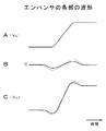
When the image signal Va is a signal having an edge and a flat portion as shown in FIG. 20A, the image signal Vb becomes as shown in FIG. 20B, and the edge portion becomes steep, but the flat portion near this edge portion. The level of changes. Due to this level change, bordering occurs on both sides of the edge portion of the image.
[0014]
In this way, the level of the flat portion near the edge portion in the image signal Vb changes when the image signal Va is a signal having an edge and a flat portion as shown in FIG. 22A. The contour signal which is the extracted high frequency component is as shown in FIG. 22B. Therefore, the image signal Vb obtained by adding the contour signal to the image signal Va becomes steep at the edge portion as shown in FIG. 22C, but the level of the flat portion near the edge portion changes.
[0015]
Here, by increasing the number of taps of the high-pass filter that extracts the high-frequency component as the contour signal, the low-frequency level of the high-frequency component can be raised. Therefore, the edge portion of the image signal Va can be steeper, and the contour of the image can be more emphasized. However, the range of the flat portion near the edge portion where the level changes is widened, and the border generated on both sides of the edge portion of the image is widened, and this border becomes more conspicuous (see the broken line portions in FIGS. 22B and 22C). ).
[0016]
Therefore, conventionally, since the edge generated on both sides of the edge portion of the image is inconspicuous, it is not possible to increase the number of taps of the high-pass filter that extracts the high-frequency component as the contour signal, and the image contour enhancement effect is sufficiently achieved. It was difficult to get to.
[0017]
In the case of the image signal Vb shown in FIG. 20B, as shown in FIG. 20C, if the edge portion remains steep and an image signal in which the level change of the flat portion near the edge portion is eliminated can be obtained. It is ideal because the outline of the image can be emphasized and no edge is generated on both sides of the edge portion.
[0018]
When the image signal Va is a signal having no flat portion as shown in FIG. 21A, the image signal Vb is as shown in FIG. 21B. In this case, the user does not feel a border on the image. Therefore, in this case, as shown in FIG. 21C, it is ideal if the same image signal as the image signal Vb can be obtained.
[0019]
In
[0020]
However, in the case of suppressing the amplitude of the contour signal in accordance with the level of the peripheral luminance signal in this way, when the level of the peripheral luminance signal is not higher than the first level or lower than the second level, the contour signal Is not performed, and the level change of the flat portion near the edge portion described above cannot be suppressed.
[0021]
Therefore, in this case, the image signal Vb shown in FIG. 20B cannot be brought close to the ideal image signal as shown in FIG. 20C, and it is difficult to reduce the conspicuous fringing on both sides of the edge portion of the image.
[0022]
In
[0023]
In this case, the level change of the flat part near the edge part of the image signal can be suppressed, and it is possible to reduce the conspicuous bordering on both sides of the edge part of the image. However, in this case, when the absolute value level of the contour signal is large, the amplitude of the contour signal is uniformly suppressed. For this reason, there is a problem in that the edge signal amplitude is suppressed and the edge emphasis effect is weakened when the absolute value level of the edge signal is large even in a portion other than the flat portion near the edge portion of the image signal where the edge is not conspicuous.
[0024]
Note that in a scaling device that converts the number of pixels in the horizontal direction and the vertical direction by interpolation processing, ringing occurs in a flat portion near the edge portion of the image signal, which causes deterioration in image quality.
[0025]
An object of the present invention is to improve the image quality of an edge portion without any inconvenience when, for example, enhancement processing or scaling processing is performed.
[0026]
[Means for Solving the Problems]
An image signal processing apparatus according to the present invention includes: an image signal processing unit that processes a first image signal composed of a plurality of pixel data to obtain a second image signal composed of a plurality of pixel data; A plurality of pixel data of the first image signal located in the vicinity of the target position The flatness is calculated from And a maximum value for detecting a maximum value of a plurality of pixel data of the first image signal located in the vicinity of the target position in the second image signal. Detection means, minimum value detection means for detecting a minimum value of a plurality of pixel data of the first image signal, which is located in the vicinity of the attention position in the second image signal, and a pixel at the attention position in the second image signal When the data value is larger than the maximum value detected by the maximum value detecting means or smaller than the minimum value detected by the minimum value detecting means, the attention in the second image signal is based on the determination result of the waveform determining means. Signal suppression means for obtaining a third image signal by suppressing the pixel data value at the position so as to approach the maximum value or the minimum value as the degree of complexity of the waveform is lower.
[0027]
The image signal processing method according to the present invention further includes a step of processing a first image signal composed of a plurality of pixel data to obtain a second image signal composed of a plurality of pixel data, and attention in the second image signal. A plurality of pixel data of the first image signal located in the vicinity of the position The flatness is calculated from A step of determining the degree of complexity of the waveform, detecting a maximum value of a plurality of pixel data of the first image signal located in the vicinity of the target position in the second image signal, Detecting a minimum value of a plurality of pixel data of the first image signal located in the vicinity of the target position in the second image signal, and detecting a value of the pixel data of the target position in the second image signal; When larger than the maximum value or smaller than the detected minimum value, based on the determination result of the degree of complexity of the waveform, the value of the pixel data at the position of interest in the second image signal is determined based on the degree of complexity of the waveform. And a step of obtaining a third image signal by suppressing the value so as to approach the maximum value or the minimum value as the value is lower.
[0028]
The image display device according to the present invention includes an image signal processing means for processing a first image signal composed of a plurality of pixel data to obtain a second image signal composed of a plurality of pixel data, and a second image signal. A plurality of pixel data of the first image signal located in the vicinity of the target position in The flatness is calculated from And a maximum value for detecting a maximum value of a plurality of pixel data of the first image signal located in the vicinity of the target position in the second image signal. Detection means, minimum value detection means for detecting a minimum value of a plurality of pixel data of the first image signal, which is located in the vicinity of the attention position in the second image signal, and a pixel at the attention position in the second image signal When the data value is larger than the maximum value detected by the maximum value detecting means or smaller than the minimum value detected by the minimum value detecting means, the attention in the second image signal is based on the determination result of the waveform determining means. The signal suppression means for obtaining the third image signal by suppressing the value of the pixel data at the position so as to approach the maximum value or the minimum value as the degree of complexity of the waveform is lower, and the third obtained by this signal suppression means Image In which and a display device for displaying an image by.
[0029]
In the present invention, a first image signal composed of a plurality of pixel data is processed to obtain a second image signal composed of a plurality of pixel data.
For example, enhancement processing (outline enhancement processing) is performed. That is, a high frequency component is extracted from the first image signal, and this high frequency component is added to the first image signal to obtain a second image signal in which the high frequency is emphasized. In this case, the level of the flat portion near the edge portion of the image signal changes, and this causes image quality degradation.
[0030]
Further, for example, scaling processing (pixel number conversion processing) is performed. That is, pixel data at an interpolation position in at least a horizontal or vertical interpolation direction is generated based on the first image signal, and a second image signal obtained by converting the number of pixels in the interpolation direction is obtained. In this case, ringing (level change) occurs in a flat portion near the edge portion of the image signal, and this causes deterioration in image quality.
[0031]
The degree of complexity of the waveform is determined based on a plurality of pixel data of the first image signal located in the vicinity of the target position in the second image signal. In this case, for example, a flat portion near the edge portion of the image signal is determined to have a low degree of waveform complexity.
[0032]
For example, a first signal indicating flatness is obtained based on a plurality of pixel data located on one side from the target position with respect to a predetermined direction that is at least a horizontal direction or a vertical direction, and the first signal indicating the flatness is obtained from the target position. A second signal indicating flatness is obtained based on a plurality of pixel data located on the side of the, and a discrimination result is obtained based on a small value signal of the first signal and the second signal.
[0033]
The maximum value and the minimum value of the plurality of pixel data of the first image signal located in the vicinity of the target position in the second image signal are detected. When the pixel data value at the target position in the second image signal is larger than the maximum value or smaller than the minimum value, the value of the pixel data at the target position in the second image signal is the waveform complexity. As the degree is lower, the third image signal is obtained by being suppressed so as to approach the maximum value or the minimum value. This suppression is performed by, for example, mixing pixel data of the target position in the second image signal and the maximum value or the minimum value at a ratio based on the determination result.
[0034]
In this way, the second image signal is subjected to the suppression process according to the degree of complexity of the waveform. The third image signal after the suppression process is supplied to the display element, and an image based on the third image signal is displayed on the display element.
[0035]
The value of the pixel data at the target position in the second image signal is suppressed so as to approach the maximum value or the minimum value as the degree of complexity of the waveform is lower. For example, when the enhancement process is performed on the first image signal to obtain the second image signal, the level change of the flat portion near the edge portion of the second image signal is suppressed. Further, for example, when the second image signal is obtained by performing the scaling process on the first image signal, ringing in a flat portion near the edge portion of the second image signal is suppressed. Thereby, the image quality of the edge portion is improved.
[0036]
Note that when the degree of complexity of the waveform is high, the pixel data at the target position in the second image signal is not suppressed. Therefore, for example, pixel data at the target position in the second image signal is not suppressed except in a flat portion near the edge portion of the second image signal, and no inconvenience occurs. For example, when the enhancement processing is performed, pixel data is not suppressed except for a flat portion near the edge portion of the second image signal where the border is not conspicuous, and the edge enhancement effect is not weakened. Further, for example, when the scaling process is performed, pixel data is not suppressed in a portion other than a flat portion near the edge portion of the second image signal where no ringing occurs, and the image quality is not deteriorated.
[0037]
The image signal processing apparatus according to the present invention comprises a scaling processing unit and an enhancement processing unit.
[0038]
The scaling processing unit generates pixel data at an interpolation position in at least a horizontal or vertical interpolation direction based on the first image signal, and obtains a second image signal obtained by converting the number of pixels in the interpolation direction. Image signal processing means, first waveform discrimination means for discriminating the degree of complexity of the waveform based on a plurality of pixel data of the first image signal located in the vicinity of the target position in the second image signal A first maximum value detecting means for detecting a maximum value of a plurality of pixel data of the first image signal located in the vicinity of the target position in the second image signal; and a vicinity of the target position in the second image signal The first minimum value detecting means for detecting the minimum value of the plurality of pixel data of the first image signal, and the value of the pixel data at the position of interest in the second image signal is the first maximum value detection Detected by means When the value is larger than the large value or smaller than the minimum value detected by the first minimum value detection means, the value of the pixel data at the target position in the second image signal is calculated based on the determination result of the waveform determination means. And a first signal suppressing means for obtaining a third image signal by suppressing the degree of complexity so as to approach the maximum value or the minimum value.
[0039]
In addition, the enhancement processing unit is positioned near the target position in the fourth image signal, second image signal processing means for enhancing the high frequency in the interpolation direction of the third image signal to obtain the fourth image signal. A second waveform discriminating means for discriminating the degree of complexity of the waveform based on a plurality of pixel data of the third image signal, and a third waveform signal positioned in the vicinity of the target position in the fourth image signal. A second maximum value detecting means for detecting a maximum value of the plurality of pixel data of the image signal; and a minimum value of the plurality of pixel data of the third image signal located in the vicinity of the target position in the fourth image signal. The second minimum value detecting means to detect and the value of the pixel data at the target position in the fourth image signal are larger than the maximum value detected by the second maximum value detecting means, or the second minimum value detection Less than the minimum value detected by the means On the basis of the discrimination result of the waveform discriminating means, the value of the pixel data at the target position in the fourth image signal is suppressed so as to approach the maximum value or the minimum value as the degree of complexity of the waveform is lower. Second signal suppression means for obtaining a signal.
[0040]
In the present invention, in the scaling processing unit, the value of the pixel data at the target position in the second image signal is suppressed so as to approach the maximum value or the minimum value as the degree of complexity of the waveform is lower, and the flatness near the edge portion is suppressed. A third image signal in which the ringing (level change) of the part is suppressed is obtained. Further, in the enhancement processing unit, the value of the pixel data at the target position in the fourth image signal is suppressed so as to approach the maximum value or the minimum value as the degree of complexity of the waveform is lower, and a flat portion near the edge portion is suppressed. A fifth image signal in which the level change is suppressed is obtained.
[0041]
In this case, since the ringing of the flat portion near the edge portion of the third image signal output from the scaling processing unit is suppressed, the enhancement processing unit performs strong contour enhancement to provide a sharp feeling. Even if it is increased, ringing does not stand out. In addition, even if strong edge enhancement is performed by the enhancement processing unit, the level change of the flat portion near the edge portion of the fifth image signal is suppressed, so that the border is conspicuous on both sides of the edge portion. Nor.
[0042]
DETAILED DESCRIPTION OF THE INVENTION
Embodiments of the present invention will be described below with reference to the drawings.
A first embodiment of the present invention will be described. FIG. 1 shows a configuration of an
The
[0043]
The operation of the
An image signal Va is input to the
[0044]
The image signal processing unit 102 will be further described.
The image signal processing unit 102 uses an image signal Va input to the
[0045]
The nonlinear
[0046]
Further, the image signal processing unit 102 adds an outline signal to which a nonlinear characteristic is given by the nonlinear
[0047]
In addition, the image signal processing unit 102 includes a horizontal high-pass filter (horizontal HPF) 125 that extracts a horizontal high-frequency component from the image signal Va as a horizontal contour signal, and a nonlinear
[0048]
Further, the image signal processing unit 102 adds the contour signal to which the non-linear characteristic is given by the non-linear
[0049]
The operation of the image signal processing unit 102 will be described.
An image signal Va as an input image signal is supplied to the vertical high-
[0050]
The
[0051]
The image signal V12 output from the
[0052]
For this reason, the vertical
[0053]
An image signal Va as an input image signal is supplied to the horizontal high-
[0054]
The
[0055]
The image signal V15 output from the
[0056]
For this reason, the horizontal
[0057]
Next, a specific configuration of the edge improving unit 150 (the vertical
[0058]
The
[0059]
In addition, the
[0060]
FIG. 3 shows an example of a plurality of pixel data of the image signal V2 used for the detection processing of the maximum value MAX and the minimum value MIN, and further for processing a to e for waveform discrimination described later. In the case of the vertical
[0061]
Here, the pixel data of n is pixel data located at the target position. The n-1 and n-2 pixel data are located on one side with respect to the n pixel data, and are pixel data one pixel before and two pixels before, respectively. The pixel data of n + 1 and n + 2 are located on the other side with respect to the pixel data of n, and are pixel data after one pixel and after two pixels, respectively.
[0062]
In the detection process of the maximum value MAX in the maximum
[0063]
Further, the
[0064]
The
[0065]
In addition, the
[0066]
In addition, the
[0067]
The
[0068]
In the processing a in the
[0069]
FIG. 5 shows an example of the nonlinear characteristic in the nonlinear
[0070]
The signal S1 indicating the flatness of the waveform of the target position obtained by the first processing unit 159 has a small value in a flat portion near the edge portion of the image signal V2. As a result, it is determined that the degree of complexity of the waveform is low in the flat portion near the edge portion.
[0071]
In addition, the
[0072]
In the processing c in the
[0073]
In addition, the
[0074]
In the processing d in the
[0075]
Further, the
[0076]
In addition, the
[0077]
In addition, the
[0078]
In the
z = x · m / 100 + y × (1−m / 100) (1)
[0079]
The operation of the
The
[0080]
The maximum
[0081]
The plurality of pixel data of the image signal V2 used for the detection processing of the maximum value MAX and the minimum value MIN, and also for the processing a to e for waveform discrimination, in the vertical
[0082]
In the
[0083]
The maximum value MAX detected by the maximum
[0084]
When SW1 = [1], and therefore x> MAX, the
[0085]
Further, the
[0086]
This discrimination result α is obtained as follows. That is, the first processing unit 159 obtains a signal S1 indicating the flatness of the waveform of the target position based on a plurality of pixel data of the image signal V2 located in the vicinity of the target position in the image signal V1. The signal S1 has a small value in a portion where the degree of complexity of the waveform is low, for example, in a flat portion near the edge portion of the image signal V2. This signal S1 is supplied to the
[0087]
Further, the
[0088]
In this case, the high frequency component S2 is used as a signal for complementing the signal S1. That is, the signal S1 obtained by the first processing unit 159 may be a small value depending on the waveform even if the waveform is complicated. In this case, since the value of the high frequency component S2 becomes large, the signal S1 can be complemented.
[0089]
Further, the
[0090]
The output signal of the
[0091]
The discrimination result α obtained by the
[0092]
When SW2 = [1], and therefore x> MAX or x <MIN, the
[0093]
The output signal m of the
[0094]
Here, consider a case where the value x of the pixel data at the target position in the image signal V1 is larger than the maximum value MAX (x> MAX). In this case, the output signal S4 of the
[0095]
Therefore, in the
[0096]
Consider a case where the value x of pixel data at the target position in the image signal V1 is smaller than the minimum value MIN (x <MIN). In this case, the output signal S4 of the
[0097]
Therefore, in the
[0098]
Also, consider the case where the value x of the pixel data at the target position in the image signal V1 is in the range from the maximum value MAX to the minimum value MIN (MIN ≦ x ≦ MAX). In this case, the output signal m of the
[0099]
In this way, in the
[0100]
Then, the
[0101]
When it is determined that the degree of complexity of the waveform is high, the determination result α increases. In this case, the degree of suppression in the
[0102]
Note that the edge portion itself is also judged to have a high degree of waveform complexity, and the discrimination result α increases. Therefore, the edge portion of the image signal V3 is placed in a state of being sharpened by enhancement processing, like the edge portion of the image signal V1. That is, the edge emphasis effect by the enhancement process is not weakened.
[0103]
Further, in the
[0104]
Note that the
[0105]
Here, examples of actual values of the respective parts (1) to (18) in the
[0106]
FIG. 7 shows an example of the value of each part in the case of a signal having an edge and a flat part (see FIG. 20). FIG. 8 shows an example of the value of each part in the case of a signal without a flat part (see FIG. 21).
[0107]
(1) is an image signal V2 input to the
[0108]
Further, (10) is an output signal of the
[0109]
Note that the processing in the image signal processing unit 102 in FIG. 1 can be realized by software, for example, by an image
[0110]
First, the image
[0111]
Further, the image
[0112]
Further, the image
[0113]
Here, instead of inputting the input image signal Va from the input terminal 314, it may be recorded in advance in the HDD 305 or downloaded from the
[0114]
A processing procedure for obtaining the output image signal Vb from the input image signal Va in the image
[0115]
First, in step ST1, processing is started, and in step ST2, the input image signal Va is input for one frame. When the input image signal Va is input from the input terminal 314, pixel data constituting the input image signal Va is temporarily stored in the RAM 303. If the input image signal Va is recorded in the HDD 305, the input image signal Va is read from the HDD 305, and the pixel data constituting the input image signal Va is temporarily stored in the RAM 303.
[0116]
Next, in step ST3, a high-frequency component in the vertical direction is extracted from the input image signal Va, and this high-frequency component is added to the image signal Va as a vertical contour signal after imparting non-linear characteristics. An image signal V12 in which the high frequency in the vertical direction is emphasized is generated by limiting the maximum value.
[0117]
Next, in step ST4, the degree of complexity of the vertical waveform of the position of interest in the image signal V12 is determined, and the determination result α is obtained. This determination is performed using a plurality of pixel data arranged in the vicinity of the target position in the image signal V12 and arranged in the vertical direction of the image signal Va.
[0118]
In step ST5, the maximum value MAX and the minimum value MIN of a plurality of pixel data arranged in the vertical direction of the image signal Va located in the vicinity of the target position in the image signal V12 are detected. In step ST6, the value of the pixel data at the target position in the image signal V12 is suppressed using the determination result α obtained in step ST4 and the maximum value MAX and the minimum value MIN detected in step ST5. The image signal V13 is generated.
[0119]
In this case, when the value x of the pixel data at the target position in the image signal V12 is larger than the maximum value MAX (x> MAX) or smaller than the minimum value MIN (x <MIN), the waveform in the vicinity of the target position. As the degree of complexity of the image signal V12 decreases, that is, as the determination result α decreases, the value x of the pixel data at the target position in the image signal V12 is suppressed so as to approach the maximum value MAX or the minimum value MIN. The value of pixel data.
[0120]
When the value x of the pixel data at the target position in the image signal V12 is in the range from the maximum value MAX to the minimum value MIN (MIN ≦ x ≦ MAX), the value x of the pixel data at the target position in the image signal V12 is set. The pixel data value of the image signal V13 is used as it is.
[0121]
Next, in step ST7, it is determined whether or not the processing for all the pixel data of the image signal V12 generated in step ST3 is completed. If not completed, the process returns to step ST4 and proceeds to the process for the next target position. On the other hand, when finished, the process proceeds to step ST8.
[0122]
In step ST8, a high frequency component in the horizontal direction is extracted from the image signal V13, and this high frequency component is added to the image signal V13 as a horizontal contour signal after adding a nonlinear characteristic, and further the maximum value of this added signal is limited. As a result, the image signal V15 in which the high frequency in the vertical and horizontal directions is emphasized is generated.
[0123]
Next, in step ST9, the degree of complexity of the horizontal waveform of the target position in the image signal V15 is determined, and the determination result α is obtained. This determination is performed using a plurality of pixel data arranged in the horizontal direction of the image signal V13, which is located in the vicinity of the target position in the image signal V15.
[0124]
In step ST10, the maximum value MAX and the minimum value MIN of a plurality of pixel data arranged in the horizontal direction of the image signal V13 located in the vicinity of the target position in the image signal V15 are detected. In step ST11, the value of the pixel data at the target position in the image signal V15 is suppressed using the determination result α obtained in step ST9 and the maximum value MAX and the minimum value MIN detected in step ST10. The output image signal Vb is generated.
[0125]
In this case, when the value x of the pixel data of the target position in the image signal V15 is larger than the maximum value MAX (x> MAX) or smaller than the minimum value MIN (x <MIN), the horizontal position near the target position is horizontal. The lower the degree of complexity of the waveform in the direction, that is, the smaller the determination result α, the smaller the value x of the pixel data at the target position in the image signal V15 so that it approaches the maximum value MAX or the minimum value MIN. The pixel data value of the signal Vb is used.
[0126]
When the value x of the pixel data at the target position in the image signal V15 is in the range from the maximum value MAX to the minimum value MIN (MIN ≦ x ≦ MAX), the value x of the pixel data at the target position in the image signal V15 is The pixel data value of the image signal Vb is used as it is.
[0127]
Next, in step ST12, it is determined whether or not the processing for all the pixel data of the image signal V15 generated in step ST8 has been completed. If not completed, the process returns to step ST9 and proceeds to the process for the next target position. On the other hand, when finished, the process proceeds to step ST13.
[0128]
In step ST13, the generated image signal Vb for one frame is output. In this case, the image signal Vb is output to the output terminal 315 or supplied to the HDD 305 for recording.
[0129]
Next, in step ST14, it is determined whether or not processing of all frames to be processed has been completed. When the processing of all the frames has not been completed, the process returns to step ST2 and proceeds to the processing of the input image signal Va for the next one frame. On the other hand, when all the frames have been processed, the process ends in step ST15.
[0130]
As described above, by performing processing according to the flowchart shown in FIG. 10, similarly to the image signal processing unit 102 in FIG. 1, the input pixel signal of the input image signal Va is processed, and the output image signal Vb is processed. Pixel data can be obtained.
[0131]
Next explained is the second embodiment of the invention. FIG. 11 shows a configuration of an
[0132]
The
[0133]
The operation of the
An image signal Va is input to the
[0134]
The image signal processing unit 102A will be further described.
The image signal processing unit 102A uses an image signal Va input to the
[0135]
The nonlinear characteristic circuit 131 sets the level of the output signal to 0 when the absolute value level of the input signal is less than or equal to a predetermined value. This prevents the noise component from being emphasized. Further, the nonlinear characteristic circuit 131 sets the level of the output signal to a constant value when the absolute value level of the input signal is equal to or greater than a predetermined value. This prevents the high-frequency signal level from being saturated.
[0136]
Further, the image signal processing unit 102A adds the contour signal to which the non-linear characteristic is given by the non-linear characteristic circuit 131 to the image signal Va to obtain an image signal V41 in which the vertical direction and the high direction in the horizontal direction are emphasized. 132, a
[0137]
The operation of the image signal processing unit 102A will be described.
An image signal Va as an input image signal is supplied to the two-dimensional high-
[0138]
The
[0139]
The image signal V42 output from the
[0140]
Therefore, the two-dimensional
[0141]
Next, a specific configuration of the two-dimensional
[0142]
The
[0143]
Further, the
[0144]
FIG. 3 described above shows an example of a plurality of pixel data used for the detection process of the maximum value MAX and the minimum value MIN and the processes a to e for waveform discrimination, and pixel data of n−2 to n + 2 Indicates pixel data arranged in the vertical or horizontal direction.
[0145]
The two-dimensional
[0146]
In the detection process of the maximum value MAX in the maximum value detection circuit 154A, pixel data of n-1, n, n + 1 in the vertical direction and pixel data of n-1, n, n + 1 in the horizontal direction are used. The maximum value is detected. In the minimum value MIN detection process in the minimum value detection circuit 155A, vertical n−1, n, n + 1 pixel data and horizontal n−1, n, n + 1 pixel data are used. The minimum value of the data is detected.
[0147]
Further, the
[0148]
The
[0149]
Further, the
[0150]
In addition, the
[0151]
This waveform determination unit 158A receives a horizontal processing unit 171H for obtaining a signal Sh indicating the degree of complexity of the waveform in the horizontal direction of the target position, and a signal Sv indicating the degree of complexity of the waveform in the vertical direction of the target position. A
[0152]
In this case, in the horizontal processing unit 171H, the processing a, the processing unit b, the processing c, the processing d, and the processing e are respectively performed as n-2, n-1, n pixel data in the horizontal direction, n + 2, n + 1, n. Pixel data, n-1, n, n + 1 pixel data, n-2, n-1, n pixel data, and n + 2, n + 1, n pixel data. On the other hand, in the
[0153]
In addition, the
[0154]
Further, the
[0155]
In the
[0156]
The operation of the
The enhanced image signal V42 is input to the
[0157]
In the maximum value detection circuit 154A, the maximum value MAX of a plurality of pixel data of the image signal Va located in the vicinity of the target position of the image signal V42 is detected. Further, the minimum value detection circuit 155A detects a minimum value MIN of a plurality of pixel data of the image signal Va located in the vicinity of the target position of the image signal V42. These maximum value MAX and minimum value MIN are supplied to the
[0158]
In the
[0159]
The maximum value MAX detected by the maximum value detection circuit 154A is supplied to the fixed terminal on the a side of the
[0160]
When SW1 = [1], and therefore x> MAX, the
[0161]
Further, the waveform discrimination unit 158A discriminates the degree of complexity of the horizontal and vertical waveforms based on a plurality of pixel data of the image signal Va located in the vicinity of the target position in the image signal V42. α is obtained. This discrimination result α becomes smaller as the degree of complexity of the waveform is lower. As the determination result α, the signal Sh indicating the complexity of the horizontal waveform generated by the horizontal processing unit 171H and the signal Sv indicating the complexity of the vertical waveform generated by the
[0162]
The discrimination result α obtained by the waveform discrimination unit 158A is supplied to the fixed terminal on the a side of the
[0163]
When SW2 = [1], and therefore x> MAX or x <MIN, the
[0164]
The output signal m of the
[0165]
Here, consider a case where the value x of the pixel data at the target position in the image signal V42 is larger than the maximum value MAX (x> MAX). In this case, the output signal S4 of the
[0166]
Therefore, in the
[0167]
Consider a case where the pixel data value x at the target position in the image signal V42 is smaller than the minimum value MIN (x <MIN). In this case, the output signal S4 of the
[0168]
Therefore, in the
[0169]
Consider a case where the value x of the pixel data at the target position in the image signal V42 is in the range from the maximum value MAX to the minimum value MIN (MIN ≦ x ≦ MAX). In this case, the output signal m of the
[0170]
As described above, the two-dimensional
[0171]
Note that the processing in the image signal processing unit 102A of FIG. 11 can be realized by software, for example, by an image
[0172]
A processing procedure for obtaining the output image signal Vb from the input image signal Va in the image
[0173]
First, in step ST21, the process is started, and in step ST22, the input image signal Va is input for one frame. When the input image signal Va is input from the input terminal 314, pixel data constituting the input image signal Va is temporarily stored in the RAM 303. If the input image signal Va is recorded in the HDD 305, the input image signal Va is read from the HDD 305, and the pixel data constituting the input image signal Va is temporarily stored in the RAM 303.
[0174]
Next, in step ST23, high frequency components in the vertical direction and horizontal direction are extracted from the input image signal Va, and these high frequency components are added to the image signal Va as vertical and horizontal contour signals after adding nonlinear characteristics. Further, the maximum value of the addition signal is further limited to generate the image signal V42 in which the high range in the vertical direction and the horizontal direction is emphasized.
[0175]
Next, in step ST24, the degree of complexity of the vertical and horizontal waveforms of the target position in the image signal V42 is determined, and the determination result α is obtained. This determination is performed using a plurality of pixel data arranged in the vertical direction and the horizontal direction of the image signal Va, which are located in the vicinity of the target position in the image signal V42.
[0176]
Next, in step ST25, the maximum value MAX and the minimum value MIN of a plurality of pixel data arranged in the vertical direction and the horizontal direction of the image signal Va located in the vicinity of the target position in the image signal V42 are detected. In step ST26, the value of the pixel data at the target position in the image signal V42 is suppressed using the determination result α obtained in step ST24 and the maximum value MAX and the minimum value MIN detected in step ST25. The image signal Vb is generated.
[0177]
In this case, when the value x of the pixel data at the target position in the image signal Vb is larger than the maximum value MAX (x> MAX) or smaller than the minimum value MIN (x <MIN), the waveform in the vicinity of the target position. As the degree of complexity of the image signal Vb decreases, that is, the determination result α decreases, the value x of the pixel data at the target position in the image signal V42 is suppressed so as to approach the maximum value MAX or the minimum value MIN. The value of pixel data.
[0178]
When the value x of the pixel data at the target position in the image signal V42 is in the range from the maximum value MAX to the minimum value MIN (MIN ≦ x ≦ MAX), the value x of the pixel data at the target position in the image signal V42 is set. The pixel data value of the image signal Vb is used as it is.
[0179]
Next, in step ST27, it is determined whether or not the processing for all the pixel data of the image signal V42 generated in step ST23 is completed. If not completed, the process returns to step ST24 to move to the process for the next target position. On the other hand, when completed, the process proceeds to step ST28.
[0180]
In step ST28, the generated image signal Vb for one frame is output. In this case, the image signal Vb is output to the output terminal 315 or supplied to the HDD 305 for recording.
[0181]
Next, in step ST29, it is determined whether or not processing of all frames to be processed has been completed. When the processing of all the frames has not been completed, the process returns to step ST22 and proceeds to the processing of the input image signal Va for the next one frame. On the other hand, when all the frames have been processed, the process ends in step ST30.
[0182]
In this way, by performing processing according to the flowchart shown in FIG. 13, the pixel data of the input image signal Va input is processed and the output image signal Vb is processed in the same manner as the image signal processing unit 102A shown in FIG. Pixel data can be obtained.
[0183]
In the image signal processing unit 102A in FIG. 11, the two-dimensional high-
[0184]
However, in this case, with respect to the oblique direction, the level of the flat portion near the edge portion changes as in the above-described vertical direction and horizontal direction, and due to this level change, bordering occurs on both sides of the edge portion of the image.
[0185]
Therefore, in this case, also in the oblique direction, as in the vertical direction and the horizontal direction described above, the level change of the flat portion near the edge portion of the image signal is suppressed, and the edges on both sides of the edge portion of the image are conspicuous. Need to be reduced.
[0186]
Therefore, as described above, when the high-frequency component in the oblique direction is also added to the image signal Va to emphasize the contour in the oblique direction, the two-dimensional
[0187]
That is, the maximum value detection circuit 154A displays a plurality of pixel data arranged in the vertical direction, the horizontal direction, the first diagonal direction, and the second diagonal direction of the image signal Va, which are located in the vicinity of the target position of the image signal V42. The maximum value MAX of these pixel data is detected.
[0188]
Similarly, the minimum value detection circuit 155A is a plurality of pixel data arranged in the vicinity of the target position of the image signal V42 and arranged in the vertical direction, the horizontal direction, the first diagonal direction, and the second diagonal direction of the image signal Va. And the minimum value MIN of these pixel data is detected.
[0189]
Further, the waveform discriminating unit 158A obtains a signal Sh indicating the degree of complexity of the waveform in the horizontal direction of the target position and a signal Sv indicating the degree of complexity of the waveform in the vertical direction of the target position. In addition to the
[0190]
These oblique processing units 171B1 and 171B2 are configured similarly to the horizontal processing unit 171H and the
[0191]
In the waveform discriminating unit 158A, signals Sb1 and Sb2 are added in addition to the signals Sh and Sv by the
[0192]
Next explained is the third embodiment of the invention. FIG. 14 shows a configuration of an
[0193]
The
[0194]
The operation of the
An image signal Va is input to the
[0195]
The image signal processing unit 102B will be further described.
The image signal processing unit 102B uses the image signal Va input to the
[0196]
The image signal processing unit 102B also includes a vertical
[0197]
Further, the image signal processing unit 102B has a
[0198]
The image signal processing unit 102B also has a horizontal
[0199]
The operation of the image signal processing unit 102B will be described.
An image signal Va as an input image signal is supplied to the
[0200]
The image signal V31 output from the
[0201]
Therefore, in the vertical
[0202]
Further, the
[0203]
The image signal V33 output from the
[0204]
Therefore, the horizontal
[0205]
Next, a specific configuration of the
[0206]
The
[0207]
In addition, the
[0208]
In addition, the
[0209]
Further, the
[0210]
The
[0211]
In addition, the
[0212]
Further, the
[0213]
In addition, the
[0214]
The image signal V2 is not used in this way. This image signal V2 is before the scaling process (pixel number conversion process), and the number of pixels is different from that of the image signal V1. This is because the waveform discrimination result α corresponding to the pixel data cannot be obtained. Note that the output signal S4 of the
[0215]
Note that the vertical
[0216]
Further, the
[0217]
In the
z = x · α / 100 + y × (1−α / 100) (2)
[0218]
The operation of the
The
[0219]
The maximum
[0220]
Further, in the minimum
[0221]
In the case of the vertical
[0222]
The maximum value MAX and the minimum value MIN obtained by the
[0223]
The maximum value MAX obtained by the interpolation circuit 181 is supplied to the fixed terminal on the a side of the
[0224]
When SW1 = [1], and therefore x> MAX, the
[0225]
The output signal S4 of the
[0226]
When SW2 = [1], and therefore x> MAX or x <MIN, the switch circuit 83 is connected to the b side, and the output signal S4 of the
[0227]
The output signal S5 of the
[0228]
The discrimination result α obtained by the
[0229]
Here, consider a case where the value x of the pixel data at the target position in the image signal V1 is larger than the maximum value MAX (x> MAX). In this case, the output signal S4 of the
[0230]
Therefore, in the
[0231]
Consider a case where the value x of pixel data at the target position in the image signal V1 is smaller than the minimum value MIN (x <MIN). In this case, the output signal S4 of the
[0232]
Therefore, in the
[0233]
Also, consider the case where the value x of the pixel data at the target position in the image signal V1 is in the range from the maximum value MAX to the minimum value MIN (MIN ≦ x ≦ MAX). In this case, the output signal S5 of the
[0234]
In this way, in the
[0235]
Then, the
[0236]
Note that the processing in the image signal processing unit 102B in FIG. 14 can be realized by software, for example, by an image
[0237]
A processing procedure for obtaining the output image signal Vb from the input image signal Va in the image
[0238]
First, in step ST41, the process is started, and in step ST42, the input image signal Va is input for one frame. When the input image signal Va is input from the input terminal 314, pixel data constituting the input image signal Va is temporarily stored in the RAM 303. If the input image signal Va is recorded in the HDD 305, the input image signal Va is read from the HDD 305, and the pixel data constituting the input image signal Va is temporarily stored in the RAM 303.
[0239]
Next, in step ST43, based on the image signal Va, pixel data at an interpolation position in the vertical direction is generated, the number of pixels is converted, and an image signal V31 is generated. In step ST44, the maximum value MAX and the minimum value MIN corresponding to the target position in the image signal V31 are detected.
[0240]
In this case, for a plurality of, for example, two pieces of pixel data arranged in the vertical direction of the image signal Va, which are located in the vicinity of the target position in the image signal V31, from the plurality of pieces of pixel data arranged in the vicinity of the pixel data. The maximum value MAX and the minimum value MIN are detected. Then, the maximum value MAX corresponding to the position of interest in the image signal V31 is obtained from a plurality of detected maximum values MAX, for example, two maximum values MAX by interpolation processing. Similarly, a minimum value MIN corresponding to the target position in the image signal V31 is obtained from a plurality of detected, for example, two minimum values MIN by interpolation processing.
[0241]
Next, in step ST45, the degree of complexity of the vertical waveform of the target position in the image signal V31 is determined, and the determination result α is obtained. This determination is performed using the maximum value MAX or the minimum value MIN corresponding to a plurality of pixel data arranged in the vertical direction of the image signal V31 located in the vicinity of the target position in the image signal V31. The plurality of maximum values MAX or minimum values MIN are obtained by the same process as in step ST44.
[0242]
In this case, when the value x of the pixel data at the target position in the image signal V31 is larger than the maximum value MAX corresponding to the target position (x> MAX), a plurality of maximum values MAX are used, while the target in the image signal V31. When the value x of the pixel data at the position is smaller than the minimum value MIN corresponding to the target position (x <MIN), a plurality of minimum values MIN are used.
[0243]
Next, in step ST46, the value of pixel data at the target position in the image signal V31 is suppressed using the maximum value MAX and the minimum value MIN detected in step ST44 and the determination result α obtained in step ST45. Thus, the image signal V32 is generated.
[0244]
In this case, when the value x of the pixel data at the target position in the image signal V31 is larger than the maximum value MAX (x> MAX) or smaller than the minimum value MIN (x <MIN), the waveform in the vicinity of the target position. As the degree of complexity of the image signal V31 decreases, that is, as the determination result α decreases, the value x of the pixel data at the target position in the image signal V31 is suppressed so as to approach the maximum value MAX or the minimum value MIN. The value of pixel data.
[0245]
When the value x of the pixel data at the target position in the image signal V31 is in the range from the maximum value MAX to the minimum value MIN (MIN ≦ x ≦ MAX), the value x of the pixel data at the target position in the image signal V31 is The pixel data value of the image signal V32 is used as it is.
[0246]
Next, in step ST47, it is determined whether or not the processing for all the pixel data of the image signal V31 generated in step ST43 is completed. If not completed, the process returns to step ST44 and proceeds to the process for the next target position. On the other hand, when completed, the process proceeds to step ST48.
[0247]
In step ST48, pixel data of the interpolation position in the horizontal direction is generated based on the image signal V32, the number of pixels is converted, and an image signal V33 is generated. In step ST49, the maximum value MAX and the minimum value MIN corresponding to the target position in the image signal V33 are detected.
[0248]
In this case, for a plurality of, for example, two pieces of pixel data arranged in the horizontal direction of the image signal V32 positioned in the vicinity of the target position in the image signal V33, the maximum is obtained from the plurality of pixel data arranged in the vicinity of the pixel data. The value MAX and the minimum value MIN are detected. Then, a maximum value MAX corresponding to the target position in the image signal V33 is obtained by interpolation processing from a plurality of detected maximum values, for example, two maximum values MAX. Similarly, a minimum value MIN corresponding to the target position in the image signal V33 is obtained from a plurality of detected, for example, two minimum values MIN by interpolation processing.
[0249]
Next, in step ST50, the degree of complexity of the horizontal waveform of the target position in the image signal V33 is determined, and the determination result α is obtained. This determination is performed using the maximum value MAX or the minimum value MIN corresponding to a plurality of pixel data arranged in the horizontal direction of the image signal V33 located in the vicinity of the target position in the image signal V33. The plurality of maximum values MAX or minimum values MIN are obtained by the same processing as in step ST49.
[0250]
In this case, when the value x of the pixel data at the target position in the image signal V33 is larger than the maximum value MAX corresponding to the target position (x> MAX), a plurality of maximum values MAX are used, while the target in the image signal V33. When the value x of the pixel data at the position is smaller than the minimum value MIN corresponding to the target position (x <MIN), a plurality of minimum values MIN are used.
[0251]
Next, in step ST51, the value of the pixel data at the target position in the image signal V33 is suppressed using the maximum value MAX and the minimum value MIN detected in step ST49 and the determination result α obtained in step ST50. Thus, the image signal Vb is generated.
[0252]
In this case, when the value x of the pixel data at the target position in the image signal V33 is larger than the maximum value MAX (x> MAX) or smaller than the minimum value MIN (x <MIN), the waveform in the vicinity of the target position. As the degree of complexity of the image signal Vb decreases, that is, the determination result α decreases, the value x of the pixel data at the target position in the image signal V33 is suppressed so as to approach the maximum value MAX or the minimum value MIN. The value of pixel data.
[0253]
When the value x of the pixel data at the target position in the image signal V33 is in the range from the maximum value MAX to the minimum value MIN (MIN ≦ x ≦ MAX), the value x of the pixel data at the target position in the image signal V33 is set. The pixel data value of the image signal Vb is used as it is.
[0254]
Next, in step ST52, it is determined whether or not the processing for all the pixel data of the image signal V33 generated in step ST48 is completed. If not completed, the process returns to step ST49 and proceeds to the process for the next target position. On the other hand, when finished, the process proceeds to step ST53.
[0255]
In step ST53, the generated image signal Vb for one frame is output. In this case, the image signal Vb is output to the output terminal 315 or supplied to the HDD 305 for recording.
[0256]
Next, in step ST54, it is determined whether or not processing of all frames to be processed has been completed. If all the frames have not been processed, the process returns to step ST42, and the process proceeds to the processing of the input image signal Va for the next one frame. On the other hand, when all the frames have been processed, the process ends in step ST55.
[0257]
In this manner, by performing processing according to the flowchart shown in FIG. 16, the pixel data of the input image signal Va input is processed in the same manner as the image signal processing unit 102B of FIG. Pixel data can be obtained.
[0258]
Next explained is the fourth embodiment of the invention. FIG. 17 shows a configuration of an
[0259]
The
[0260]
The operation of the
An image signal Va is input to the
[0261]
In this case, pixel data at the interpolation positions in the horizontal direction and the vertical direction are generated based on the image signal Va, thereby converting the numbers of pixels in the horizontal direction and the vertical direction. This interpolation is performed by a conventionally known method such as linear interpolation, cubic interpolation or nearest neighbor interpolation. Further, the high-frequency components in the horizontal direction and the vertical direction are extracted from the image signal V34 after the scaling process, and the high-frequency components are added to the image signal V34, thereby obtaining the image signal Vb in which the high frequency is emphasized. .
[0262]
The image signal Vb obtained by the image signal processing unit 102 </ b> C is supplied to the
[0263]
The image signal processing unit 102C will be further described.
The image signal processing unit 102C uses the image signal Va input to the
[0264]
Further, the image signal processing unit 102C suppresses a ringing (level change) generated in a flat portion near the edge portion in the vertical direction in the image signal V31 output from the vertical interpolation circuit 140 (see FIG. 5). 15).
[0265]
Further, the image signal processing unit 102C includes a
[0266]
The image signal processing unit 102C also suppresses ringing (level change) generated in a flat portion near the edge portion in the horizontal direction in the image signal V33 output from the horizontal interpolation circuit 142 (see FIG. 5). 15).
[0267]
The image signal processing unit 102C also includes a vertical high-pass filter (vertical HPF) 120 that extracts a vertical high-frequency component as a vertical contour signal from the scaled image signal V34 output from the horizontal
[0268]
Further, the image signal processing unit 102C adds the contour signal to which the non-linear characteristic is given by the non-linear
[0269]
The image signal processing unit 102C also has a horizontal high-pass filter (horizontal HPF) 125 that extracts a horizontal high-frequency component as a horizontal contour signal from the image signal V34 after scaling processing, and a non-linearity that imparts non-linear characteristics to the contour signal. And a
[0270]
Further, the image signal processing unit 102C adds the contour signal to which the non-linear characteristic is given by the non-linear
[0271]
The
[0272]
The operation of the image signal processing unit 102C will be described.
An image signal Va as an input image signal is supplied to the
[0273]
The image signal V31 output from the
[0274]
Therefore, in the vertical
[0275]
Further, the
[0276]
The image signal V33 output from the
[0277]
Therefore, the horizontal
[0278]
The scaled image signal V 34 output from the horizontal
[0279]
The
[0280]
The image signal V12 output from the
[0281]
For this reason, the vertical
[0282]
The image signal V34 is supplied to the horizontal high-
[0283]
The
[0284]
The image signal V15 output from the
[0285]
For this reason, the horizontal
[0286]
In this image signal processing unit 102C, the ringing of the flat portion near the edge portion of the image signal V34 output from the scaling processing unit is suppressed, so that the enhancement processing unit performs strong edge enhancement. Even if the sharpness is enhanced, ringing does not stand out. Even if the enhancement processing unit performs strong contour emphasis, the level change of the flat portion near the edge portion of the image signal Vb is suppressed, so that the border is not conspicuous on both sides of the edge portion. .
[0287]
In the image signal processing unit 102C described above, the enhancement processing unit has the same configuration as that of the image signal processing unit 102 in FIG. 1, but this enhancement processing unit has the same configuration as that of the image signal processing unit 102A in FIG. It can also be.
[0288]
The configuration of the
[0289]
In the above-described embodiment, when the level of a flat portion near the edge portion of the image signal changes due to enhancement processing or scaling processing, the change is suppressed by the edge improvement unit. When image signal processing that causes a level change is performed, it is a matter of course that the level change can be satisfactorily suppressed by adopting the same configuration as that of the above-described embodiment.
[0290]
The image signal processing apparatus of FIG. 18 shows a general configuration in that case. The input image signal V2 input to the
[0291]
【The invention's effect】
According to the present invention, when the value of the pixel data at the target position in the processed image signal is larger than the maximum value or smaller than the minimum value of the pixel data in the vicinity of the target position in the unprocessed image signal, the target As the degree of complexity of the waveform in the vicinity of the position is lower, the pixel data value of the target position in the processed image signal is suppressed so as to approach the maximum value or the minimum value. For example, enhancement processing or scaling processing is performed. Etc., the image quality of the edge portion can be improved without causing any inconvenience.
[Brief description of the drawings]
FIG. 1 is a block diagram illustrating a configuration of an image display device according to a first embodiment.
FIG. 2 is a block diagram illustrating a configuration of an edge improvement unit.
FIG. 3 is a diagram illustrating pixel data used for each process of an edge improvement unit.
FIG. 4 is a diagram illustrating processing contents of each processing of an edge improvement unit.
FIG. 5 is a diagram illustrating an example of coefficient values of a high-pass filter (11 taps) for extracting a high frequency component as an outline enhancement signal.
FIG. 6 is a diagram illustrating an example of nonlinear characteristics.
FIG. 7 is a diagram showing values of respective parts in the case of a signal having an edge and a flat part.
FIG. 8 is a diagram illustrating values of respective parts in the case of a signal without a flat part.
FIG. 9 is a block diagram illustrating a configuration example of an image signal processing device to be realized by software.
FIG. 10 is a flowchart showing a processing procedure (enhancement processing) of an image signal.
FIG. 11 is a block diagram illustrating a configuration of an image display device according to a second embodiment.
FIG. 12 is a block diagram illustrating a configuration of a two-dimensional edge improvement unit.
FIG. 13 is a flowchart illustrating a processing procedure (enhancement processing) of an image signal.
FIG. 14 is a block diagram illustrating a configuration of an image display device according to a third embodiment.
FIG. 15 is a block diagram illustrating a configuration of an edge improvement unit.
FIG. 16 is a flowchart showing a processing procedure (scaling processing) of an image signal.
FIG. 17 is a block diagram illustrating a configuration of an image display device according to a fourth embodiment.
FIG. 18 is a block diagram showing a general image processing apparatus according to the present invention.
FIG. 19 is a block diagram showing a configuration of a conventional enhancer.
FIG. 20 is a diagram illustrating a waveform of each part during enhancement processing in the case of a signal having an edge and a flat part.
FIG. 21 is a diagram illustrating a waveform of each part at the time of enhancement processing in the case of a signal without a flat part.
FIG. 22 is a diagram for explaining waveforms at various parts of a conventional enhancer.
[Explanation of symbols]
DESCRIPTION OF SYMBOLS 100,100A-100C ... Image display apparatus, 101 ... Input terminal, 102, 102A-102C ... Image signal processing part, 103 ... Panel driver, 104 ... Display element, 120 ... Vertical high-pass filter, 121, 126, 131 ... nonlinear characteristic circuit, 122, 127, 132 ... adder, 123, 128, 133 ... limiter, 124 ... vertical edge improvement unit, 125 ... Horizontal high-pass filter, 129... Horizontal edge improvement unit, 130... Two-dimensional high-pass filter, 134... Two-dimensional edge improvement unit, 140. ... horizontal interpolation circuit, 143 ... horizontal edge improvement unit, 150, 150B ... edge improvement unit, 151, 152 ... input terminal, 153 Output terminals, 154, 154A, 154B ... maximum value detection circuit, 155, 155A, 155B ... minimum value detection circuit, 156 ... amplitude comparison circuit, 157, 165 ... switch circuit, 158, 158A ... Waveform discriminating section, 159 ... First processing section, 160 ... Second processing section, 161 ... Third processing section, 162 ... Adder, 163 ...
Claims (11)
上記第2の画像信号における注目位置の近傍に位置する、上記第1の画像信号の複数の画素データから平坦度を求め、当該平坦度に基づいて、波形の複雑さの度合いを判別する波形判別手段と、
上記第2の画像信号における注目位置の近傍に位置する、上記第1の画像信号の複数の画素データの最大値を検出する最大値検出手段と、
上記第2の画像信号における注目位置の近傍に位置する、上記第1の画像信号の複数の画素データの最小値を検出する最小値検出手段と、
上記第2の画像信号における注目位置の画素データの値が、上記最大値検出手段で検出される最大値より大きいとき、または上記最小値検出手段で検出される最小値より小さいとき、上記波形判別手段の判別結果に基づき、上記第2の画像信号における注目位置の画素データの値を、上記波形の複雑さの度合いが低い程上記最大値または上記最小値に近づくように抑圧して第3の画像信号を得る信号抑圧手段と
を備える画像信号処理装置。Image signal processing means for processing a first image signal comprising a plurality of pixel data to obtain a second image signal comprising a plurality of pixel data;
Waveform discrimination for obtaining flatness from a plurality of pixel data of the first image signal located in the vicinity of the target position in the second image signal and determining the degree of complexity of the waveform based on the flatness Means,
Maximum value detecting means for detecting a maximum value of a plurality of pixel data of the first image signal, which is located in the vicinity of a target position in the second image signal;
Minimum value detecting means for detecting a minimum value of a plurality of pixel data of the first image signal, which is located in the vicinity of the target position in the second image signal;
When the value of the pixel data at the target position in the second image signal is larger than the maximum value detected by the maximum value detecting means or smaller than the minimum value detected by the minimum value detecting means, the waveform discrimination Based on the determination result of the means, the value of the pixel data at the target position in the second image signal is suppressed so as to approach the maximum value or the minimum value as the degree of complexity of the waveform decreases, images signal processing device Ru and a signal suppressing means for obtaining an image signal.
少なくとも水平方向または垂直方向である所定方向に関して上記注目位置から一の側に位置する複数の画素データに基づいて平坦度を示す第1の信号を求めると共に、上記所定方向に関して上記注目位置から他の側に位置する複数の画素データに基づいて平坦度を示す第2の信号を求め、上記第1の信号および上記第2の信号のうち小さな値の信号を出力する第1の処理部を有し、該第1の処理部より出力される信号に基づいて判別結果を得る請求項1に記載の画像信号処理装置。The waveform discrimination means is
A first signal indicating flatness is obtained based on a plurality of pixel data located on one side of the target position with respect to a predetermined direction which is at least a horizontal direction or a vertical direction, and another signal is obtained from the target position with respect to the predetermined direction. A first processing unit that obtains a second signal indicating flatness based on a plurality of pixel data located on the side and outputs a signal having a smaller value out of the first signal and the second signal; the image signal processing apparatus according to discrimination results based on the signal output from the first processing unit to obtain Ru請 Motomeko 1.
上記所定方向に関して上記注目位置から上記一の側および上記他の側に位置する複数の画素データに基づいて高域成分を抽出する第2の処理部をさらに有し、
上記第1の処理部より出力される信号と上記第2の処理部で抽出される高域成分との和信号に基づいて判別結果を得る請求項2に記載の画像信号処理装置。The waveform discrimination means is
A second processing unit for extracting a high frequency component based on a plurality of pixel data located on the one side and the other side from the target position with respect to the predetermined direction;
The image signal processing apparatus according to 請 Motomeko 2 to give Ru a discrimination result based on the sum signal of a high-frequency component extracted by the signal and the second processing unit output from the first processing unit.
上記所定方向に関して上記注目位置から上記一の側に位置する複数の画素データに基づいて第1の高域成分を抽出すると共に、上記所定方向に関して上記注目位置から上記他の側に位置する複数の画素データに基づいて第2の高域成分を抽出し、上記第1の高域成分および上記第2の高域成分のうち小さな値の高域成分を出力する第3の処理部をさらに有し、
上記第1の処理部より出力される信号と上記第2の処理部で抽出される高域成分との和信号から上記第3の処理部より出力される高域成分を差し引いて得られる差信号に基づいて判別結果を得る請求項3に記載の画像信号処理装置。The waveform discrimination means is
A first high-frequency component is extracted based on a plurality of pixel data positioned on the one side from the target position with respect to the predetermined direction, and a plurality of positions positioned on the other side from the target position with respect to the predetermined direction. A third processing unit for extracting a second high-frequency component based on the pixel data and outputting a high-frequency component having a small value out of the first high-frequency component and the second high-frequency component; ,
A difference signal obtained by subtracting the high frequency component output from the third processing unit from the sum signal of the signal output from the first processing unit and the high frequency component extracted by the second processing unit. the image signal processing apparatus according to obtain Ru請 Motomeko 3 the discrimination result on the basis of.
上記第2の画像信号における注目位置の画素データと、上記最大値検出手段で検出される最大値または上記最小値検出手段で検出される最小値とを、上記判別結果に基づいた比率で混合する請求項1に記載の画像信号処理装置。The signal suppression means is
The pixel data of the target position in the second image signal and the maximum value detected by the maximum value detection unit or the minimum value detected by the minimum value detection unit are mixed at a ratio based on the determination result. the image signal processing apparatus according to 請 Motomeko 1 that.
上記第1の画像信号から高域成分を抽出するハイパスフィルタと、
上記ハイパスフィルタで抽出される高域成分を上記第1の画像信号に加算して高域が強調された上記第2の画像信号を得る加算器とを有する請求項1に記載の画像信号処理装置。The image signal processing means;
A high pass filter for extracting a high frequency component from the first image signal;
Image according to 請 Motomeko 1 that have a adder to obtain a high frequency component is added to the first image signal highs emphasized the second image signal extracted by the high-pass filter Signal processing device.
上記第1の画像信号に基づいて、少なくとも水平または垂直の補間方向における補間位置の画素データを生成し、該補間方向の画素数を変換した上記第2の画像信号を得る補間回路を有する請求項1に記載の画像信号処理装置。The image signal processing means includes:
Based on the first image signal, that at least to generate pixel data of the interpolation position in the horizontal or vertical interpolation direction, having a interpolation circuit for obtaining the second image signal obtained by converting the number of pixels interpolation direction the image signal processing apparatus according to 請 Motomeko 1.
上記第2の画像信号における注目位置の近傍に位置する、上記第1の画像信号の複数の画素データから平坦度を求め、当該平坦度に基づいて、波形の複雑さの度合いを判別する第1の波形判別手段と、
上記第2の画像信号における注目位置の近傍に位置する、上記第1の画像信号の複数の画素データの最大値を検出する第1の最大値検出手段と、
上記第2の画像信号における注目位置の近傍に位置する、上記第1の画像信号の複数の画素データの最小値を検出する第1の最小値検出手段と、
上記第2の画像信号における注目位置の画素データの値が、上記第1の最大値検出手段で検出される最大値より大きいとき、または上記第1の最小値検出手段で検出される最小値より小さいとき、上記波形判別手段の判別結果に基づき、上記第2の画像信号における注目位置の画素データの値を、上記波形の複雑さの度合いが低い程上記最大値または上記最小値に近づくように抑圧して第3の画像信号を得る第1の信号抑圧手段と、
上記第3の画像信号の上記補間方向の高域を強調して第4の画像信号を得る第2の画像信号処理手段と、
上記第4の画像信号における注目位置の近傍に位置する、上記第3の画像信号の複数の画素データに基づいて、波形の複雑さの度合いを判別する第2の波形判別手段と、
上記第4の画像信号における注目位置の近傍に位置する、上記第3の画像信号の複数の画素データの最大値を検出する第2の最大値検出手段と、
上記第4の画像信号における注目位置の近傍に位置する、上記第3の画像信号の複数の画素データの最小値を検出する第2の最小値検出手段と、
上記第4の画像信号における注目位置の画素データの値が、上記第2の最大値検出手段で検出される最大値より大きいとき、または上記第2の最小値検出手段で検出される最小値より小さいとき、上記第2の波形判別手段の判別結果に基づき、上記第4の画像信号における注目位置の画素データの値を、上記波形の複雑さの度合いが低い程上記最大値または上記最小値に近づくように抑圧して第5の画像信号を得る第2の信号抑圧手段とを備える画像信号処理装置。First image signal processing means for generating pixel data at an interpolation position in at least a horizontal or vertical interpolation direction based on the first image signal and obtaining a second image signal obtained by converting the number of pixels in the interpolation direction; ,
A flatness is obtained from a plurality of pixel data of the first image signal located in the vicinity of the target position in the second image signal, and a degree of complexity of the waveform is determined based on the flatness . Waveform discrimination means,
First maximum value detecting means for detecting a maximum value of a plurality of pixel data of the first image signal, which is located in the vicinity of a target position in the second image signal;
First minimum value detecting means for detecting a minimum value of a plurality of pixel data of the first image signal, which is located in the vicinity of a target position in the second image signal;
When the value of the pixel data at the target position in the second image signal is larger than the maximum value detected by the first maximum value detection unit, or from the minimum value detected by the first minimum value detection unit When it is small, the value of the pixel data at the target position in the second image signal is made closer to the maximum value or the minimum value as the degree of complexity of the waveform is lower, based on the determination result of the waveform determination means. First signal suppression means for suppressing and obtaining a third image signal;
Second image signal processing means for emphasizing a high frequency region in the interpolation direction of the third image signal to obtain a fourth image signal;
Second waveform discrimination means for discriminating the degree of complexity of the waveform based on a plurality of pixel data of the third image signal located in the vicinity of the target position in the fourth image signal;
Second maximum value detecting means for detecting a maximum value of a plurality of pixel data of the third image signal, which is located in the vicinity of the target position in the fourth image signal;
Second minimum value detecting means for detecting a minimum value of a plurality of pixel data of the third image signal located in the vicinity of the target position in the fourth image signal;
When the value of the pixel data at the target position in the fourth image signal is larger than the maximum value detected by the second maximum value detection unit, or from the minimum value detected by the second minimum value detection unit When it is small, based on the determination result of the second waveform determining means, the value of the pixel data at the target position in the fourth image signal is set to the maximum value or the minimum value as the degree of complexity of the waveform is lower. approaches such suppressed to fifth images signal processing device Ru and a second signal suppressing means for obtaining an image signal of.
上記第2の画像信号における注目位置の近傍に位置する、上記第1の画像信号の複数の画素データから平坦度を求め、当該平坦度に基づいて、波形の複雑さの度合いを判別するステップと、
上記第2の画像信号における注目位置の近傍に位置する、上記第1の画像信号の複数の画素データの最大値を検出するステップと、
上記第2の画像信号における注目位置の近傍に位置する、上記第1の画像信号の複数の画素データの最小値を検出するステップと、
上記第2の画像信号における注目位置の画素データの値が、上記検出される最大値より大きいとき、または上記検出される最小値より小さいとき、上記波形の複雑さの度合いの判別結果に基づき、上記第2の画像信号における注目位置の画素データの値を、上記波形の複雑さの度合いが低い程上記最大値または上記最小値に近づくように抑圧して第3の画像信号を得るステップとを備える画像信号処理方法。Processing a first image signal comprising a plurality of pixel data to obtain a second image signal comprising a plurality of pixel data;
Obtaining flatness from a plurality of pixel data of the first image signal located in the vicinity of the target position in the second image signal, and determining a degree of complexity of the waveform based on the flatness ; ,
Detecting a maximum value of a plurality of pixel data of the first image signal located in the vicinity of a target position in the second image signal;
Detecting a minimum value of a plurality of pixel data of the first image signal located in the vicinity of a target position in the second image signal;
When the value of the pixel data of the target position in the second image signal is larger than the detected maximum value or smaller than the detected minimum value, based on the determination result of the degree of complexity of the waveform, A step of obtaining a third image signal by suppressing the value of pixel data at the target position in the second image signal so that the degree of complexity of the waveform is lower so as to approach the maximum value or the minimum value. comprising Ru images signal processing method.
上記第2の画像信号における注目位置の近傍に位置する、上記第1の画像信号の複数の画素データから平坦度を求め、当該平坦度に基づいて、波形の複雑さの度合いを判別する波形判別手段と、
上記第2の画像信号における注目位置の近傍に位置する、上記第1の画像信号の複数の画素データの最大値を検出する最大値検出手段と、
上記第2の画像信号における注目位置の近傍に位置する、上記第1の画像信号の複数の画素データの最小値を検出する最小値検出手段と、
上記第2の画像信号における注目位置の画素データの値が、上記最大値検出手段で検出される最大値より大きいとき、または上記最小値検出手段で検出される最小値より小さいとき、上記波形判別手段の判別結果に基づき、上記第2の画像信号における注目位置の画素データの値を、上記波形の複雑さの度合いが低い程上記最大値または上記最小値に近づくように抑圧して第3の画像信号を得る信号抑圧手段と、
上記信号抑圧手段で得られる第3の画像信号による画像を表示する表示素子とを備える画像表示装置。Image signal processing means for processing a first image signal comprising a plurality of pixel data to obtain a second image signal comprising a plurality of pixel data;
Waveform discrimination for obtaining flatness from a plurality of pixel data of the first image signal located in the vicinity of the target position in the second image signal and determining the degree of complexity of the waveform based on the flatness Means,
Maximum value detecting means for detecting a maximum value of a plurality of pixel data of the first image signal, which is located in the vicinity of a target position in the second image signal;
Minimum value detecting means for detecting a minimum value of a plurality of pixel data of the first image signal, which is located in the vicinity of the target position in the second image signal;
When the value of the pixel data at the target position in the second image signal is larger than the maximum value detected by the maximum value detecting means or smaller than the minimum value detected by the minimum value detecting means, the waveform discrimination Based on the determination result of the means, the value of the pixel data at the target position in the second image signal is suppressed so as to approach the maximum value or the minimum value as the degree of complexity of the waveform decreases, Signal suppression means for obtaining an image signal;
The signal a third image signal obtained by suppressing means images display Ru and a display device for displaying an image by.
Priority Applications (1)
| Application Number | Priority Date | Filing Date | Title |
|---|---|---|---|
| JP2003057638A JP4135083B2 (en) | 2003-03-04 | 2003-03-04 | Image signal processing apparatus and processing method, and image display apparatus using the same |
Applications Claiming Priority (1)
| Application Number | Priority Date | Filing Date | Title |
|---|---|---|---|
| JP2003057638A JP4135083B2 (en) | 2003-03-04 | 2003-03-04 | Image signal processing apparatus and processing method, and image display apparatus using the same |
Publications (2)
| Publication Number | Publication Date |
|---|---|
| JP2004266775A JP2004266775A (en) | 2004-09-24 |
| JP4135083B2 true JP4135083B2 (en) | 2008-08-20 |
Family
ID=33120995
Family Applications (1)
| Application Number | Title | Priority Date | Filing Date |
|---|---|---|---|
| JP2003057638A Expired - Fee Related JP4135083B2 (en) | 2003-03-04 | 2003-03-04 | Image signal processing apparatus and processing method, and image display apparatus using the same |
Country Status (1)
| Country | Link |
|---|---|
| JP (1) | JP4135083B2 (en) |
Families Citing this family (4)
| Publication number | Priority date | Publication date | Assignee | Title |
|---|---|---|---|---|
| JP5087368B2 (en) * | 2007-10-30 | 2012-12-05 | 株式会社エヌ・ティ・ティ・ドコモ | Image processing apparatus, image processing method, and image processing program |
| JPWO2011105365A1 (en) * | 2010-02-26 | 2013-06-20 | シャープ株式会社 | Image processing apparatus, display apparatus including the same, and image processing method |
| WO2012124591A1 (en) * | 2011-03-15 | 2012-09-20 | シャープ株式会社 | Signal processing device, control program, and integrated circuit |
| CN112966620A (en) * | 2021-03-15 | 2021-06-15 | 北京鹰瞳科技发展股份有限公司 | Fundus image processing method, model training method and equipment |
-
2003
- 2003-03-04 JP JP2003057638A patent/JP4135083B2/en not_active Expired - Fee Related
Also Published As
| Publication number | Publication date |
|---|---|
| JP2004266775A (en) | 2004-09-24 |
Similar Documents
| Publication | Publication Date | Title |
|---|---|---|
| EP2114067B1 (en) | Image processing apparatus and image processing method, and program | |
| JP5115361B2 (en) | Pixel interpolation device, pixel interpolation method, and pixel interpolation program | |
| US8098334B2 (en) | System and process for image rescaling with edge adaptive phase control in interpolation process | |
| CN102063703B (en) | System for enhancing input image, image display system and method for enhancing image | |
| EP1480166A1 (en) | An edge enhancement process and system | |
| US8279346B2 (en) | Frame rate converting apparatus and method thereof | |
| JP2003274218A (en) | Sharpness improving method and apparatus thereof | |
| JP5479064B2 (en) | Image processing apparatus, control method therefor, and program | |
| CN102918830A (en) | Image processing apparatus, method therefor, image display apparatus, and method therefor | |
| JP2000137469A (en) | Pixel number converter | |
| JP2004266775A (en) | Image signal processing apparatus and processing method, and image display apparatus using the same | |
| EP2632145A1 (en) | Signal processing device, signal processing method, signal processing program, and display device | |
| JP3508404B2 (en) | Image display device | |
| KR20030082249A (en) | Motion adaptive spatial-temporal deinterlacing method | |
| WO2012073865A1 (en) | Image processing device, image processing method, image processing program, and display device | |
| JP2003123066A (en) | Image reduction display method and device | |
| JP4762115B2 (en) | Video processing device | |
| JPH11203467A (en) | Display device and display method | |
| JP5121639B2 (en) | Image processing apparatus and image processing method | |
| JP2006030352A (en) | Liquid crystal display | |
| CN101287075B (en) | Video signal processing device, video signal processing method and image display device | |
| JP5018198B2 (en) | Interpolation signal generation circuit, interpolation signal generation method, program, and video signal processing apparatus | |
| KR100725208B1 (en) | Digital image signal processing device and method | |
| JP2004194044A (en) | Image display device | |
| JP2000115720A (en) | Scanning line interpolation device and scanning line interpolation method |
Legal Events
| Date | Code | Title | Description |
|---|---|---|---|
| A621 | Written request for application examination |
Free format text: JAPANESE INTERMEDIATE CODE: A621 Effective date: 20051110 |
|
| RD04 | Notification of resignation of power of attorney |
Free format text: JAPANESE INTERMEDIATE CODE: A7424 Effective date: 20060502 |
|
| A977 | Report on retrieval |
Free format text: JAPANESE INTERMEDIATE CODE: A971007 Effective date: 20080229 |
|
| A131 | Notification of reasons for refusal |
Free format text: JAPANESE INTERMEDIATE CODE: A131 Effective date: 20080304 |
|
| A521 | Request for written amendment filed |
Free format text: JAPANESE INTERMEDIATE CODE: A523 Effective date: 20080411 |
|
| TRDD | Decision of grant or rejection written | ||
| A01 | Written decision to grant a patent or to grant a registration (utility model) |
Free format text: JAPANESE INTERMEDIATE CODE: A01 Effective date: 20080508 |
|
| A01 | Written decision to grant a patent or to grant a registration (utility model) |
Free format text: JAPANESE INTERMEDIATE CODE: A01 |
|
| A61 | First payment of annual fees (during grant procedure) |
Free format text: JAPANESE INTERMEDIATE CODE: A61 Effective date: 20080521 |
|
| FPAY | Renewal fee payment (event date is renewal date of database) |
Free format text: PAYMENT UNTIL: 20110613 Year of fee payment: 3 |
|
| FPAY | Renewal fee payment (event date is renewal date of database) |
Free format text: PAYMENT UNTIL: 20120613 Year of fee payment: 4 |
|
| FPAY | Renewal fee payment (event date is renewal date of database) |
Free format text: PAYMENT UNTIL: 20130613 Year of fee payment: 5 |
|
| LAPS | Cancellation because of no payment of annual fees |