JP4134627B2 - High frequency acoustic wave device using aluminum nitride piezoelectric thin film - Google Patents
High frequency acoustic wave device using aluminum nitride piezoelectric thin film Download PDFInfo
- Publication number
- JP4134627B2 JP4134627B2 JP2002225488A JP2002225488A JP4134627B2 JP 4134627 B2 JP4134627 B2 JP 4134627B2 JP 2002225488 A JP2002225488 A JP 2002225488A JP 2002225488 A JP2002225488 A JP 2002225488A JP 4134627 B2 JP4134627 B2 JP 4134627B2
- Authority
- JP
- Japan
- Prior art keywords
- piezoelectric film
- electrode
- acoustic wave
- electrode fingers
- wave device
- Prior art date
- Legal status (The legal status is an assumption and is not a legal conclusion. Google has not performed a legal analysis and makes no representation as to the accuracy of the status listed.)
- Expired - Fee Related
Links
Images


Description
【0001】
【発明が属する技術分野】
本発明は、通信機器等に用いられるラム波型弾性波共振器等弾性波素子に関する。
【0002】
【従来の技術】
従来、高周波用途の弾性波共振器として、ダイアモンドを用いた弾性表面波素子が知られている(例えば、特許第02885349号)。音速が8000m/sと大きいため、2.5GHz帯の弾性波素子として利用されている。
【0003】
【発明が解決しようとする課題】
通信機器用途の弾性波素子は、プロセス負荷の低減を考慮すると、より高音速が望まれる。最も高音速な材料であるダイアモンドは10000m/s以上と非常に大きい音速を有するが、しかし圧電性を有さないため、圧電体を付加する必要があり、その結果、利用できる音速は8000m/sまで低化してしまうという問題がある。
【0004】
通信機器用途のSAW素子では、より電気機械結合係数(k2)の大きい共振器を用いた方が低損失な電気特性にすることができる。高性能なSAW素子を作成する場合、ダイアモンドを用いた弾性表面波素子のk2は2%以下であり、小さいという問題がある。
本発明の目的は、上記問題点を解決すること、すなわち、音速の非常に大きい(>9000m/s)弾性波素子を提供することである。第2の目的は、k2の大きい(>2%)弾性波素子を提供することである。
【0005】
【課題を解決するための手段】
上記目的は、窒化アルミニウム(AlN)を主成分とする圧電膜と、前記圧電膜表面に形成され、少なくても二本以上の電極指を有する電極パターンとよりなるラム波型弾性波素子において、前記AlN圧電膜の分極方位(c軸)は圧電膜の法線とほぼ直交し、且つ電極指ともほぼ直交する方向であり、圧電膜の厚さは前記電極パターンの電極ピッチより薄いことを特徴とするラム波型弾性波素子により、解決する。ここでラム波型弾性波とは平板を伝搬する弾性波であり、平板の厚さ方向に対してほぼ均一なエネルギー分布を示す(例えば特許第2936210号)。
【0006】
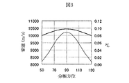
以下、本発明の作用を図を用いて説明する。図1はラム波型弾性波素子の構造を説明する断面図である。図2はラム波型弾性波の音速とk2の板厚依存性を示している。厚さhのAlN圧電膜1の表面に周期Pで2種類の電位の電極指(3-1、3-2)が交互に形成されている。電極指の幅Lと各電極間間隙Sの比は2対3である。AlN圧電膜1は矢印9で示された方向に分極したAlN圧電体を主成分とする物質で構成されている。計算は、有限要素-解析解結合法(例えば礒部敦、疋田光孝、浅井健吾、住岡淳司「有限要素-解析解結合法による新モード型SAWの探索とその移動通信用素子への応用」電子情報通信学会論文誌 C-I Vol. J 82-C-I No. 12 pp. 697-705 1999年12月)に、仮想境界での電気開放と機械開放条件を加えることで計算を行なった。図2に示すように、h<Pのラム波型弾性波で、高音速(>9000m/s)、高k2 (>2%)が得られることを見出した。図3はラム波型弾性波の音速とk2の電極指方向依存性を示している。横軸はAlN圧電膜の分極方向と電極指の方向との成す角度を示している。分極方向と電極指の方向が直交(90度)するとき、最も音速とk2が大きくなる。また55°から125°の間の角度のとき、高k2 (>2%)が得られる。すなわち、AlN圧電単結晶基板を電極指のピッチより薄くし、かつ分極方向と電極指の方向が55°から125°の間の角度のとき、高音速で高k2のラム波型弾性波素子を形成することができる。以上の考察により、一例として図1に示されるように、ギャップに挟まれた圧電膜1と、圧電膜1の表面に形成され、少なくても二本以上の電極指を有する櫛型電極パターン3を有し、圧電膜1の厚さhが電極指3のピッチPより小さい弾性波素子において、圧電膜1の主成分が窒化アルミニウムであり、圧電膜1の分極方向9が圧電膜の法線と垂直であり、且つ電極指3が圧電膜1の分極方向に対して55〜125°の範囲の角度に設定されていることを特徴とする窒化アルミニウム圧電薄膜を用いた高周波弾性波素子を提案する。
【0007】
【発明の実施の形態】
以下本発明の好ましい実施例について詳細に説明する。
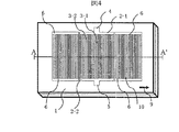
図4は本発明の第1実施例による一開口共振器の構成を示す平面図である。一開口共振器は、AlN圧電薄膜1と、その表面に形成された櫛型電極と反射器とで形成されている。櫛型電極は、AlN圧電薄膜1の分極方向9に対して平行な2本のバスバー2と、分極方向9に対して垂直な11対の電極指3と、入出力端子4、5とで構成されている。入力端子4は11本の電極指3-1に接続されたバスバー2-1に接続され、また出力端子は12本の電極指3-2に接続されたバスバー2-2に接続され、入力側の電極指3-1と出力側の電極指3-2は交互に配置されている。櫛型電極の両側に反射器が設置されている。各反射器はAlN圧電薄膜の分極方向と平行な2本のバスバー6と、分極方向と垂直な18本の反射電極指10で構成され、全ての反射電極指10の両端はバスバー6と接続されている。櫛型電極と入出力端子と反射器はAl-0.7%Cu合金により形成されている。
【0008】
図5は図4A-A'で示される部分の断面図である。AlN圧電薄膜1の厚さhは0.03P(P=20μm)に設定されている。また電極指線幅Lは0.4Pである。AlN圧電薄膜1は珪素単結晶基板7により支持されている。
このように構成された一開口共振器では、櫛型電極部のAlN圧電薄膜1の厚さが電極指ピッチPより極めて小さいため、櫛型電極で励振された弾性振動は瞬時にAlN圧電薄膜1の裏面に到達し、そのため弾性表面波ではなくラム波として伝搬する。また、弾性表面波の弾性振動は電極から深さ方向に2P程度の範囲に分布するのに対し、本一開口共振器は電極に極めて近い領域(<0.03P)に集中するため、弾性表面波より大きい圧電効果を示す。さらに、AlN圧電薄膜1の分極方向とラム波の伝播方向が一致しているため、弾性振動の主成分が縦波になり、いっそう高音速、強圧電効果となる。その結果、極めて大きい音速(>9000m/s)と比帯域幅(>0.02)を有するラム波型弾性波共振器を実現することが可能となる。
図6は他の実施例による一開口共振器の構成を示す平面図である。
図7は図6のB-B'で示される部分の断面図である。厚さh=0.1PのAlN圧電薄膜1と、その表面に形成された櫛型電極と反射器と入出力端子と、凹部を有する珪素単結晶基板7で構成されている。第1実施例とは、珪素単結晶基板7の形状が異なっているが、全く同機能のラム波型弾性波共振器を実現している。
【0009】
【発明の効果】
以上説明したように、本発明によれば、極めて大きい音速(>9000m/s)とk2 (>0.02)を有するラム波型弾性波素子を実現することができる。
弾性表面波デバイスのプロセスで広く用いられているi線露光機の微細解像できる寸法は0.30μm以上であるため、通常の弾性表面波デバイス(音速4000m/s)の適用周波数は3.3GHz以下、またダイアモンドを用いた弾性表面波デバイス(音速8000m/s)でも6.7GHz以下であるのに対して、本発明(音速9000m/s)を用いることで、7.5GHzまで拡大することができる。
【図面の簡単な説明】
【図1】本発明の弾性波素子の構造を説明する断面図。
【図2】本発明の弾性波素子の音速とk2のAlN圧電薄膜膜厚依存性を示した図。
【図3】本発明の弾性波素子の音速とk2のAlN圧電薄膜分極方向依存性を示した図。
【図4】本発明の実施の形態に係る弾性波共振器を示した斜視図。
【図5】図4のA-A'部分の断面図。
【図6】本発明の実施の形態に係る弾性波共振器を示した斜視図。
【図7】図6のB-B'部分の断面図。
【符号の説明】
1…AlN圧電薄膜。
2…バスバー。
3…電極指。
4、5…入出力端子。
6…反射器のバスバー。
7…珪素単結晶基板。
8…空隙。
9…AlNの分極方向。[0001]
[Technical field to which the invention belongs]
The present invention relates to an elastic wave element such as a lamb wave type elastic wave resonator used in communication equipment or the like.
[0002]
[Prior art]
Conventionally, a surface acoustic wave element using diamond is known as an acoustic wave resonator for high frequency applications (for example, Japanese Patent No. 02885349). Since the sound velocity is as high as 8000 m / s, it is used as an elastic wave device in the 2.5 GHz band.
[0003]
[Problems to be solved by the invention]
The acoustic wave device for communication equipment is desired to have a higher sound speed in consideration of reduction of process load. Diamond, which is the highest sound speed material, has a very high sound speed of 10000 m / s or more, but since it does not have piezoelectricity, it is necessary to add a piezoelectric material, so that the available sound speed is 8000 m / s There is a problem that it will be lowered.
[0004]
In a SAW element for communication equipment, it is possible to obtain electrical characteristics with low loss by using a resonator having a larger electromechanical coupling coefficient (k 2 ). When producing a high-performance SAW element, k 2 of a surface acoustic wave element using diamond is 2% or less, which is a problem.
An object of the present invention is to solve the above-described problems, that is, to provide an acoustic wave device having a very high sound velocity (> 9000 m / s). The second object is to provide an elastic wave device having a large k 2 (> 2%).
[0005]
[Means for Solving the Problems]
In the Lamb wave type acoustic wave device comprising a piezoelectric film mainly composed of aluminum nitride (AlN) and an electrode pattern formed on the surface of the piezoelectric film and having at least two electrode fingers, The polarization orientation (c-axis) of the AlN piezoelectric film is substantially perpendicular to the normal line of the piezoelectric film and substantially perpendicular to the electrode fingers, and the thickness of the piezoelectric film is smaller than the electrode pitch of the electrode pattern. This is solved by the Lamb wave type elastic wave element. Here, the Lamb wave type elastic wave is an elastic wave propagating through a flat plate and shows a substantially uniform energy distribution in the thickness direction of the flat plate (for example, Japanese Patent No. 2936210).
[0006]
The operation of the present invention will be described below with reference to the drawings. FIG. 1 is a cross-sectional view illustrating the structure of a Lamb wave type elastic wave device. FIG. 2 shows the dependence of the sound velocity of Lamb wave type elastic wave on the plate thickness of k2. On the surface of the AlN
[0007]
DETAILED DESCRIPTION OF THE INVENTION
Hereinafter, preferred embodiments of the present invention will be described in detail.
FIG. 4 is a plan view showing the configuration of the one-opening resonator according to the first embodiment of the present invention. The one-opening resonator is formed by an AlN piezoelectric
[0008]
FIG. 5 is a cross-sectional view of the portion shown in FIG. 4A-A ′. The thickness h of the AlN piezoelectric
In the one-opening resonator configured as described above, since the thickness of the AlN piezoelectric
FIG. 6 is a plan view showing a configuration of a one-opening resonator according to another embodiment.
FIG. 7 is a cross-sectional view of a portion indicated by BB ′ in FIG. An AlN piezoelectric
[0009]
【The invention's effect】
As described above, according to the present invention, it is possible to realize a Lamb wave type acoustic wave device having an extremely high sound velocity (> 9000 m / s) and k 2 (> 0.02).
Since the i-line exposure machine widely used in the surface acoustic wave device process has a resolution of 0.30 μm or more, the applicable frequency of ordinary surface acoustic wave devices (sonic velocity 4000 m / s) is 3.3 GHz or less. The surface acoustic wave device using diamond (sonic speed of 8000 m / s) is 6.7 GHz or lower, but by using the present invention (sound speed of 9000 m / s), it can be expanded to 7.5 GHz.
[Brief description of the drawings]
FIG. 1 is a cross-sectional view illustrating the structure of an acoustic wave device of the present invention.
FIG. 2 is a graph showing the dependence of sound velocity and k 2 on the AlN piezoelectric thin film thickness of the acoustic wave device of the present invention.
FIG. 3 is a graph showing the dependence of acoustic velocity and k 2 on the polarization direction of an AlN piezoelectric thin film of the acoustic wave device of the present invention.
FIG. 4 is a perspective view showing an acoustic wave resonator according to an embodiment of the present invention.
FIG. 5 is a cross-sectional view taken along line AA ′ of FIG.
FIG. 6 is a perspective view showing an acoustic wave resonator according to an embodiment of the present invention.
7 is a cross-sectional view taken along the line BB ′ in FIG.
[Explanation of symbols]
1 ... AlN piezoelectric thin film.
2 ... Bus bar.
3 ... Electrode fingers.
4, 5 ... Input / output terminals.
6 ... Reflector busbar.
7: A silicon single crystal substrate.
8: Void.
9: Polarization direction of AlN.
Claims (6)
前記圧電膜に形成され、少なくとも二本以上の電極指を有する櫛型電極パターンとを有し、
前記圧電膜の厚さは前記電極指のピッチより小さく、前記圧電膜内をラム波型弾性波が伝搬するよう構成され、
前記電極指の方向が前記圧電膜の分極方向に対して55°〜125°の範囲の角度に設定され、かつ、前記圧電膜の前記分極方向が前記圧電膜の法線に対して略垂直であり、かつ、前記電極指の方向が前記圧電膜の法線に対してほぼ垂直である
ことを特徴とする高周波弾性波素子。A piezoelectric film sandwiched between gaps;
A comb-shaped electrode pattern formed on the piezoelectric film and having at least two electrode fingers;
The thickness of the piezoelectric film is smaller than the pitch of the electrode fingers, and a lamb wave type elastic wave propagates in the piezoelectric film,
The direction of the electrode finger is set to an angle in a range of 55 ° to 125 ° with respect to the polarization direction of the piezoelectric film, and the polarization direction of the piezoelectric film is substantially perpendicular to the normal line of the piezoelectric film. And a direction of the electrode finger is substantially perpendicular to a normal line of the piezoelectric film .
前記櫛型電極パターンは、前記圧電膜の表面に形成されていることを特徴とする高周波弾性波素子。In claim 1,
The high frequency acoustic wave device, wherein the comb electrode pattern is formed on a surface of the piezoelectric film.
前記圧電膜は窒化アルミニウムを含んで成ることを特徴とする高周波弾性波素子。In claim 1,
The high-frequency acoustic wave device according to claim 1, wherein the piezoelectric film comprises aluminum nitride.
前記電極指の幅と前記電極指間の間隙との比が、2対3であることを特徴とする高周波弾性波素子。In any one of Claims 1 thru | or 3,
The high-frequency acoustic wave device according to claim 1, wherein a ratio of a width of the electrode finger to a gap between the electrode fingers is 2 to 3.
前記ピッチは前記弾性波の波長の1/2の長さであることを特徴とする高周波弾性波素子。In any of claims 1 to 4,
The high-frequency acoustic wave device according to claim 1, wherein the pitch is half the wavelength of the acoustic wave.
前記第1の開口部と重なる部分を有して前記第1の面上に形成された圧電膜と、
前記圧電膜上に形成され、第1の複数の電極指を有する第1の電極パターンと、
前記圧電膜上に形成され、第2の複数の電極指を有する第2の電極パターンとを具備して成り、
前記第1の複数の電極指と前記第2の複数の電極指とは、所定の周期でそれぞれ交互に配置され、
前記圧電膜の厚さは前記所定の周期より小さく、前記圧電膜内をラム波型弾性波が伝搬するよう構成され、
前記第1および第2の複数の電極指の方向は、前記圧電膜の分極方向に対して55°〜125°の範囲の角度であり、かつ、前記圧電膜の前記分極方向が前記圧電膜の法線に対して略垂直であり、かつ、前記電極指の方向が前記圧電膜の法線に対してほぼ垂直である
ことを特徴とする弾性波共振器。A substrate having a first surface and a hollow portion having an opening opening in the first surface;
A piezoelectric film formed on the first surface having a portion overlapping the first opening;
A first electrode pattern formed on the piezoelectric film and having a first plurality of electrode fingers;
A second electrode pattern formed on the piezoelectric film and having a second plurality of electrode fingers;
The first plurality of electrode fingers and the second plurality of electrode fingers are alternately arranged with a predetermined period,
The piezoelectric film has a thickness smaller than the predetermined period, and is configured such that a Lamb wave type elastic wave propagates in the piezoelectric film,
The direction of the first and second electrode fingers is an angle in the range of 55 ° to 125 ° with respect to the polarization direction of the piezoelectric film, and the polarization direction of the piezoelectric film is that of the piezoelectric film. An acoustic wave resonator characterized by being substantially perpendicular to a normal line and a direction of the electrode finger being substantially perpendicular to a normal line of the piezoelectric film .
Priority Applications (1)
| Application Number | Priority Date | Filing Date | Title |
|---|---|---|---|
| JP2002225488A JP4134627B2 (en) | 2002-08-02 | 2002-08-02 | High frequency acoustic wave device using aluminum nitride piezoelectric thin film |
Applications Claiming Priority (1)
| Application Number | Priority Date | Filing Date | Title |
|---|---|---|---|
| JP2002225488A JP4134627B2 (en) | 2002-08-02 | 2002-08-02 | High frequency acoustic wave device using aluminum nitride piezoelectric thin film |
Publications (3)
| Publication Number | Publication Date |
|---|---|
| JP2004072204A JP2004072204A (en) | 2004-03-04 |
| JP2004072204A5 JP2004072204A5 (en) | 2005-10-20 |
| JP4134627B2 true JP4134627B2 (en) | 2008-08-20 |
Family
ID=32013098
Family Applications (1)
| Application Number | Title | Priority Date | Filing Date |
|---|---|---|---|
| JP2002225488A Expired - Fee Related JP4134627B2 (en) | 2002-08-02 | 2002-08-02 | High frequency acoustic wave device using aluminum nitride piezoelectric thin film |
Country Status (1)
| Country | Link |
|---|---|
| JP (1) | JP4134627B2 (en) |
Families Citing this family (4)
| Publication number | Priority date | Publication date | Assignee | Title |
|---|---|---|---|---|
| JP2007202087A (en) | 2005-05-11 | 2007-08-09 | Seiko Epson Corp | Lamb wave type high frequency device |
| JP4613960B2 (en) * | 2005-10-19 | 2011-01-19 | 株式会社村田製作所 | Lamb wave device |
| JP4315174B2 (en) * | 2006-02-16 | 2009-08-19 | セイコーエプソン株式会社 | Manufacturing method of lamb wave type high frequency device |
| CN108470823B (en) * | 2018-04-12 | 2021-09-07 | 中国电子科技集团公司第四十九研究所 | High-voltage electric polarization system for high-molecular film |
-
2002
- 2002-08-02 JP JP2002225488A patent/JP4134627B2/en not_active Expired - Fee Related
Also Published As
| Publication number | Publication date |
|---|---|
| JP2004072204A (en) | 2004-03-04 |
Similar Documents
| Publication | Publication Date | Title |
|---|---|---|
| TWI762832B (en) | Surface acoustic wave device | |
| JP5046961B2 (en) | High frequency acoustic wave device | |
| CN1902817B (en) | Boundary acoustic wave device | |
| CN105811913A (en) | Acoustic wave device | |
| JP2008148338A (en) | Surface acoustic wave functional element | |
| JP2001524295A (en) | Surface acoustic wave device including separated comb electrodes | |
| KR20200131188A (en) | Elastic wave device, radio-frequency front-end circuit, and communication apparatus | |
| CN110995194B (en) | Two-dimensional high-performance resonator | |
| CN113056873A (en) | Elastic wave device, branching filter, and communication device | |
| JPH08288788A (en) | Surface acoustic wave element | |
| CN115001438A (en) | Structure of longitudinal leakage surface acoustic wave resonator and filter | |
| KR20190115081A (en) | A seismic device | |
| WO2023035235A1 (en) | Resonator, filter, and electronic device | |
| JP4134627B2 (en) | High frequency acoustic wave device using aluminum nitride piezoelectric thin film | |
| JP2000183681A (en) | Surface acoustic wave device | |
| JP2002152007A (en) | Lamb wave type elastic wave resonator | |
| JPH11298286A (en) | Surface acoustic wave waveguide structure and device using the structure | |
| US6373353B1 (en) | Surface acoustic wave transducer using NSPUDT property substrate and surface acoustic wave filter using the transducer | |
| WO2023097531A1 (en) | Bulk acoustic wave resonator, filter and electronic device | |
| CN116233709A (en) | High-performance acoustic device based on longitudinal acoustic surface wave | |
| JP2008092610A (en) | Surface acoustic wave substrate and surface acoustic wave functional element | |
| KR102607899B1 (en) | elastic wave device | |
| JPH10173467A (en) | Transversal saw filter | |
| JPS59213A (en) | Surface acoustic wave device | |
| WO2022168799A1 (en) | Elastic wave device |
Legal Events
| Date | Code | Title | Description |
|---|---|---|---|
| A521 | Written amendment |
Free format text: JAPANESE INTERMEDIATE CODE: A523 Effective date: 20050624 |
|
| A621 | Written request for application examination |
Free format text: JAPANESE INTERMEDIATE CODE: A621 Effective date: 20050624 |
|
| RD01 | Notification of change of attorney |
Free format text: JAPANESE INTERMEDIATE CODE: A7421 Effective date: 20060419 |
|
| A977 | Report on retrieval |
Free format text: JAPANESE INTERMEDIATE CODE: A971007 Effective date: 20070228 |
|
| A131 | Notification of reasons for refusal |
Free format text: JAPANESE INTERMEDIATE CODE: A131 Effective date: 20070327 |
|
| A521 | Written amendment |
Free format text: JAPANESE INTERMEDIATE CODE: A523 Effective date: 20070521 |
|
| A131 | Notification of reasons for refusal |
Free format text: JAPANESE INTERMEDIATE CODE: A131 Effective date: 20071016 |
|
| A521 | Written amendment |
Free format text: JAPANESE INTERMEDIATE CODE: A523 Effective date: 20071210 |
|
| TRDD | Decision of grant or rejection written | ||
| A01 | Written decision to grant a patent or to grant a registration (utility model) |
Free format text: JAPANESE INTERMEDIATE CODE: A01 Effective date: 20080507 |
|
| A01 | Written decision to grant a patent or to grant a registration (utility model) |
Free format text: JAPANESE INTERMEDIATE CODE: A01 |
|
| A61 | First payment of annual fees (during grant procedure) |
Free format text: JAPANESE INTERMEDIATE CODE: A61 Effective date: 20080520 |
|
| FPAY | Renewal fee payment (event date is renewal date of database) |
Free format text: PAYMENT UNTIL: 20110613 Year of fee payment: 3 |
|
| FPAY | Renewal fee payment (event date is renewal date of database) |
Free format text: PAYMENT UNTIL: 20110613 Year of fee payment: 3 |
|
| FPAY | Renewal fee payment (event date is renewal date of database) |
Free format text: PAYMENT UNTIL: 20120613 Year of fee payment: 4 |
|
| FPAY | Renewal fee payment (event date is renewal date of database) |
Free format text: PAYMENT UNTIL: 20120613 Year of fee payment: 4 |
|
| FPAY | Renewal fee payment (event date is renewal date of database) |
Free format text: PAYMENT UNTIL: 20130613 Year of fee payment: 5 |
|
| LAPS | Cancellation because of no payment of annual fees |