JP4131775B2 - Ferrule assembly and optical module - Google Patents
Ferrule assembly and optical module Download PDFInfo
- Publication number
- JP4131775B2 JP4131775B2 JP2000281215A JP2000281215A JP4131775B2 JP 4131775 B2 JP4131775 B2 JP 4131775B2 JP 2000281215 A JP2000281215 A JP 2000281215A JP 2000281215 A JP2000281215 A JP 2000281215A JP 4131775 B2 JP4131775 B2 JP 4131775B2
- Authority
- JP
- Japan
- Prior art keywords
- ferrule
- groove
- optical
- optical fiber
- hole
- Prior art date
- Legal status (The legal status is an assumption and is not a legal conclusion. Google has not performed a legal analysis and makes no representation as to the accuracy of the status listed.)
- Expired - Fee Related
Links
Images


Classifications
-
- G—PHYSICS
- G02—OPTICS
- G02B—OPTICAL ELEMENTS, SYSTEMS OR APPARATUS
- G02B6/00—Light guides; Structural details of arrangements comprising light guides and other optical elements, e.g. couplings
- G02B6/24—Coupling light guides
- G02B6/36—Mechanical coupling means
- G02B6/3628—Mechanical coupling means for mounting fibres to supporting carriers
- G02B6/3632—Mechanical coupling means for mounting fibres to supporting carriers characterised by the cross-sectional shape of the mechanical coupling means
- G02B6/3636—Mechanical coupling means for mounting fibres to supporting carriers characterised by the cross-sectional shape of the mechanical coupling means the mechanical coupling means being grooves
-
- G—PHYSICS
- G02—OPTICS
- G02B—OPTICAL ELEMENTS, SYSTEMS OR APPARATUS
- G02B6/00—Light guides; Structural details of arrangements comprising light guides and other optical elements, e.g. couplings
- G02B6/24—Coupling light guides
- G02B6/26—Optical coupling means
- G02B6/30—Optical coupling means for use between fibre and thin-film device
-
- G—PHYSICS
- G02—OPTICS
- G02B—OPTICAL ELEMENTS, SYSTEMS OR APPARATUS
- G02B6/00—Light guides; Structural details of arrangements comprising light guides and other optical elements, e.g. couplings
- G02B6/24—Coupling light guides
- G02B6/36—Mechanical coupling means
- G02B6/3628—Mechanical coupling means for mounting fibres to supporting carriers
- G02B6/3648—Supporting carriers of a microbench type, i.e. with micromachined additional mechanical structures
- G02B6/3652—Supporting carriers of a microbench type, i.e. with micromachined additional mechanical structures the additional structures being prepositioning mounting areas, allowing only movement in one dimension, e.g. grooves, trenches or vias in the microbench surface, i.e. self aligning supporting carriers
-
- G—PHYSICS
- G02—OPTICS
- G02B—OPTICAL ELEMENTS, SYSTEMS OR APPARATUS
- G02B6/00—Light guides; Structural details of arrangements comprising light guides and other optical elements, e.g. couplings
- G02B6/24—Coupling light guides
- G02B6/36—Mechanical coupling means
- G02B6/3628—Mechanical coupling means for mounting fibres to supporting carriers
- G02B6/3684—Mechanical coupling means for mounting fibres to supporting carriers characterised by the manufacturing process of surface profiling of the supporting carrier
- G02B6/3692—Mechanical coupling means for mounting fibres to supporting carriers characterised by the manufacturing process of surface profiling of the supporting carrier with surface micromachining involving etching, e.g. wet or dry etching steps
-
- G—PHYSICS
- G02—OPTICS
- G02B—OPTICAL ELEMENTS, SYSTEMS OR APPARATUS
- G02B6/00—Light guides; Structural details of arrangements comprising light guides and other optical elements, e.g. couplings
- G02B6/24—Coupling light guides
- G02B6/36—Mechanical coupling means
- G02B6/3628—Mechanical coupling means for mounting fibres to supporting carriers
- G02B6/3684—Mechanical coupling means for mounting fibres to supporting carriers characterised by the manufacturing process of surface profiling of the supporting carrier
- G02B6/3696—Mechanical coupling means for mounting fibres to supporting carriers characterised by the manufacturing process of surface profiling of the supporting carrier by moulding, e.g. injection moulding, casting, embossing, stamping, stenciling, printing, or with metallic mould insert manufacturing using LIGA or MIGA techniques
-
- G—PHYSICS
- G02—OPTICS
- G02B—OPTICAL ELEMENTS, SYSTEMS OR APPARATUS
- G02B6/00—Light guides; Structural details of arrangements comprising light guides and other optical elements, e.g. couplings
- G02B6/24—Coupling light guides
- G02B6/42—Coupling light guides with opto-electronic elements
- G02B6/4201—Packages, e.g. shape, construction, internal or external details
- G02B6/4219—Mechanical fixtures for holding or positioning the elements relative to each other in the couplings; Alignment methods for the elements, e.g. measuring or observing methods especially used therefor
- G02B6/4228—Passive alignment, i.e. without a detection of the degree of coupling or the position of the elements
- G02B6/423—Passive alignment, i.e. without a detection of the degree of coupling or the position of the elements using guiding surfaces for the alignment
Landscapes
- Physics & Mathematics (AREA)
- General Physics & Mathematics (AREA)
- Optics & Photonics (AREA)
- Optical Couplings Of Light Guides (AREA)
- Mechanical Coupling Of Light Guides (AREA)
Description
【0001】
【発明の属する技術分野】
本発明は、光ファイバを内蔵し光部品との接続を行うフェルールアセンブリに関し、特に、該フェルールアセンブリを使用したレセプタクル型光伝送モジュールに関する。
【0002】
近年の情報通信分野においては、情報量の増大に伴い大量の情報を高速で伝送する必要が生じており、現在光加入者系を初めとした高速・大容量な光通信網の普及が進められている。光加入者系を普及させるためには、光モジュールの低価格化が不可避の課題となる。
【0003】
光モジュールの価格は、部品費、組み立て費、試験及び調整費からなり、特に組み立て費と調整費が大きな部分を占めている。組み立て費低減の手段として、近年レセプタクル型光モジュールが脚光を浴びている。
【0004】
【従来の技術】
通信装置に組み込まれるプリント配線板に実装される部品は、一般に表面実装型とスルーホール実装型に分類される。表面実装型部品の代表例はLSIであり、フラットパッケージ型といわれる形状をしている。
【0005】
この部品はリフロー半田付けという方法によって半田付けが行われる。即ち、ペースト状の半田をプリント配線板に印刷し、このペースト半田部分に表面実装型部品を粘着させ、半田の表面温度が220℃以上となるコンベアー炉の中で半田付けを行う。
【0006】
スルーホール実装型部品の代表例は、大容量コンデンサや端子数の多い(200端子以上)LSIである。端子数の多いLSIはPGA(Pin Grid Array)という端子形態を成している。
【0007】
これらのスルーホール実装型部品はフロー半田付けという方法によって半田付けが行われる。即ち、スルーホール実装型部品の端子をプリント配線板のスルーホールに挿入し、プリント配線板を部品実装面と反対の側から260℃程度の半田槽に入れ、半田付けを行う。
【0008】
ところで、光モジュールを表面実装型部品又はスルーホール実装型部品と同様に半田付け工程でプリント配線板上に実装するには、所謂ピグテール型と呼ばれる光ファイバコード付き光モジュールは不向きである。
【0009】
通常、光ファイバコードはナイロン製被覆を有しており、このナイロン製被覆は耐熱性が80℃程度しかないため半田付け工程で溶けてしまう。また、光ファイバコード自体が製造現場において収容や取扱いの不具合をもたらし、プリント配線板への実装効率を著しく低下させることになる。
【0010】
このため、光モジュールの半田付け工程を可能として製造コストの低減を図るには、光ファイバコードを含まない所謂レセプタクル型光モジュールの提供が不可欠となっている。
【0011】
レセプタクル型光モジュールは、光モジュールにコネクタ部を設け、熱に弱い被覆付き光ファイバコードを着脱可能にしたものである。レセプタクル型光モジュールでは、高温の半田リフロー工程の適用が可能となり、光モジュールを表面実装型の電子部品と同時にプリント配線板に搭載することが可能となる。
【0012】
光部品及び電子部品を同時にプリント配線板上に搭載することにより、従来必要とされてきた融点の異なる半田による複数回の実装工程を簡易化することができ、大幅なコストの削減を見込める。
【0013】
また、調整費低減の手段としてセルフアライメント技術が検討されている。これは、光部品搭載基板上に光部品との位置関係を高精度に規定したガイド部を形成し、光導波部品(光ファイバ、フェルール等)をガイドに沿って搭載することにより、光結合を行うものである。セルフアライメント技術により、大きな工数・費用を必要とするアライメント工程を省くことが可能となる。
【0014】
特開平11−264920号は、PLC(平面光導波回路:Planer Lightwave Circuit)と光ファイバとのインタフェース部の構造を開示している。この公開公報に記載された光モジュールは光ファイバを内蔵したフェルールを光素子搭載基板に形成した溝に沿って搭載する構造を有している。溝と光部品の相対位置を精密に設計することにより、光結合を自動的(セルフ・アライメント)に行うことが可能になるという特徴を有している。
【0015】
特開平7−318764号に開示された光モジュールでは、セルフ・アライメントを行う別の形態として、フェルール端からベア光ファイバを突出させ、光素子搭載基板上に形成したガイド溝に光ファイバを挿入・固定するという方法を提案している。この構造では、ガイド溝で直接光ファイバの位置合わせを行うことができるため、より高い実装精度を得ることができるという特徴を有している。
【0016】
他の従来技術として、特開平2000−171668号が挙げられる。この公開公報に記載された光モジュールでは、セルフ・アライメントを行う別の形態として、フェルールの一部を切り欠いてベア光ファイバを半分露出させ、光素子搭載基板上に設けたガイド溝に搭載・固定するという手法を提案している。
【0017】
この構造の光モジュールでは、フェルールの一部をベア光ファイバの押さえに使っているため、押さえ部品を省略することができるだけではなく、接着領域も小さくすることができるという特徴を有している。
【0018】
【発明が解決しようとする課題】
低価格且つ信頼性の高いレセプタクル型光モジュールに要求される特性として、(1)実装が容易であること、(2)強度が高いこと、(3)端面研磨が可能であり反射対策が施せること、(4)位置合わせ精度が高いこと、の4点が挙げられる。
【0019】
特に端面研磨加工は、反射対策の手段として大きな期待が寄せられている。近年その低減化が大きな課題となっている反射戻り光を現状の25dB程度から、将来必要な40dB以上に低減化するためには、ファイバ端面を光軸に対して傾斜させた斜め研磨構造が有効である。この構造の実現には、ファイバ端が研磨加工可能なことが必要となる。
【0020】
上述した特開平11−264926号に記載された光モジュールでは、次のような問題がある。フェルールの半径に相当する深さのガイド溝を形成する必要があり(標準規格のMU型フェルールの場合約650μm)エッチング時間が増大し、保護膜の形成が困難である。また、光部品搭載基板も大型のものが必要となる。
【0021】
大きなガイド溝は形成の際に幅の制御性が低く、長時間のエッチングによって斜面に異常なエッチング面が形成され易い。更に、フェルールの外形を用いて位置合わせをするために、フェルール内径の偏心及び光ファイバ挿入時の偏心による光結合損失が発生する。
【0022】
特開平7−318764号に開示された光モジュールは次のような問題を有している。光ファイバの端面研磨が不可能である。また、光ファイバがフェルールより完全に露出しているため、取り回し時の破損の危険性が高い。
【0023】
更に、光モジュール内で光ファイバ固定部とフェルール固定部が独立しているため、光ファイバとフェルールの境界部で応力が発生し、信頼性に悪影響を及ぼす可能性がある。
【0024】
特開平2000−171668号に開示された光モジュールは以下のような問題を有している。ファイバ折損の危険が大きいため端面研磨が不可能である。また、切欠平坦部ではベア光ファイバをフェルールに固定することができないため、光ファイバ破損の危険性がある。
【0025】
よって、本発明の目的は、低コスト、小型化に適したレセプタクル型光モジュールを提供することである。
【0026】
本発明の他の目的は、レセプタクル型光モジュールを組み立てるのに要求されるフェルールアセンブリを提供することである。
【0027】
【課題を解決するための手段】
本発明によると、フェルールアセンブリであって、貫通孔と、第1端部と、該第1端部の反対側の第2端部と、該第1及び第2端部の間の中間部分を有するフェルールと;前記貫通孔中に挿入されて固定された光ファイバとを具備し;前記フェルールは前記貫通孔中に挿入された光ファイバが半分露出するような切欠平坦部を前記中間部分に有しており、前記光ファイバは前記フェルールの少なくとも前記第1及び第2端部においてその全周を該フェルールにより保持されているとともに、該光ファイバの全長が該フェルールに接触し保持されていることを特徴とするフェルールアセンブリが提供される。
【0028】
好ましくは、フェルールは第1端部及び/又は第2端部に切削加工部を有している。
【0029】
本発明のフェルールアセンブリによると、従来技術では満たすことが不可能であった上述した4つの要求項目を全て実現することができる。
【0030】
(1) フェルールの両端において光ファイバがその全周でフェルールに固定されているため、標準規格のMU型フェルール並みの取り回しが可能であり、実装が容易である。
【0031】
(2) フェルールの両端において光ファイバがその全周でフェルールに固定されているため、光ファイバ折損の危険性がない。
【0032】
(3) フェルール及び光ファイバの端面研磨加工が可能である。
【0033】
(4) ベア光ファイバによる高精度なセルフアライメントが可能である。
【0034】
本発明の他の側面によると、ブロック型フェルールアセンブリであって、貫通孔と、第1端部と、該第1端部の反対側の第2端部と、該第1及び第2端部の間の中間部分を有するブロックと;前記貫通孔中に挿入されて固定された光ファイバと;前記ブロックの前記第1端部に固定された複数のガイドピンとを具備し;前記ブロックは前記貫通孔中に挿入された光ファイバが半分露出するような切欠平坦部を前記中間部分に有しており、前記光ファイバは前記ブロックの前記第1及び第2端部においてその全周を該ブロックにより保持されているとともに、該光ファイバの全長が該ブロックに接触し保持されていることを特徴とするブロック型フェルールアセンブリが提供される。
【0035】
本発明の更に他の側面によると、光モジュールであって、第1の溝と該第1の溝に直交する第2の溝を有する基板と;一端が前記第1の溝の一端に整列した光導波路コア部と該光導波路コア部を覆った光導波路クラッド部とを有する、前記基板上に形成された光導波構造と;貫通孔と、第1端部と、該第1端部の反対側の第2端部と、該第1及び第2端部の間の中間部分を有するフェルールと;前記貫通孔中に挿入されて固定された光ファイバとを具備し;前記フェルールは前記貫通孔中に挿入された光ファイバが半分露出するような切欠平坦部を前記中間部分に有し、前記光ファイバは前記フェルールの少なくとも前記第1及び第2端部においてその全周を該フェルールにより保持されており;前記フェルールの前記第1端部が前記第2の溝中に挿入され、前記光ファイバの一端が前記光導波路コア部の一端に突き当てられるように前記光ファイバが前記基板の第1の溝中に挿入されて、前記フェルールが前記切欠平坦部で前記基板に固定されていることを特徴とする光モジュールが提供される。
【0036】
本発明の更に他の側面によると、光モジュールであって、第1の溝と該第1の溝に直交する第2の溝を有する第1基板と;第3の溝と該第3の溝に直交する第4の溝を有する第2基板と;一端が前記第1の溝の一端に整列した第1光導波路コア部と該第1光導波路コア部を覆った第1光導波路クラッド部とを有する、前記第1基板上に形成された第1光導波構造と;一端が前記第3の溝の一端に整列した第2光導波路コア部と該第2光導波路コア部を覆った第2光導波路クラッド部とを有する、前記第2基板上に形成された第2光導波構造と;貫通孔と、第1端部と、該第1端部の反対側の第2端部とを有するフェルールと;前記貫通孔中に挿入されて固定された光ファイバとを具備し;前記フェルールは前記貫通孔中に挿入された光ファイバが半分露出するような第1及び第2切欠平坦部を有し、前記光ファイバは前記フェルールの少なくとも前記第1及び第2端部においてその全周を該フェルールにより保持されており;前記フェルールの前記第1端部が前記第1基板の前記第2の溝中に挿入され、第2端部が前記第2基板の前記第4の溝中に挿入され、前記光ファイバの一端が前記第1光導波路コア部の一端に突き当てられ、他端が前記第2光導波路コア部の一端に突き当てられるように、前記光ファイバが前記第1及び第2基板の前記第1及び第3の溝中に挿入されて、前記フェルールが前記第1及び第2切欠平坦部で前記第1及び第2基板にそれぞれ固定されていることを特徴とする光モジュールが提供される。
【0037】
本発明の更に他の側面によると、光モジュールであって、表面上に第1マーカーの形成された基板と;光導波路コア部と該光導波路コア部を覆った幅の狭い第1部分と幅の広い第2部分とを有する光導波路クラッド部とを含んだ、前記基板上に形成された光導波構造と;幅の広い第1の溝と、幅の狭い第2の溝と、該第1及び第2の溝に直交するように該第1及び第2の溝の間に形成された第3の溝と、第2マーカーとを有し、該第2マーカーが前記第1マーカーに位置合わせされて前記第1の溝が前記光導波路クラッド部の前記第1部分を収容するように前記基板上に固定されたプレートと;貫通孔と、第1端部と、第2端部と、該第1及び第2端部の間の中間部分を有するフェルールと、前記貫通孔中に挿入されて固定された光ファイバとを含み、前記フェルールは前記貫通孔中に挿入された光ファイバが半分露出するような切欠平坦部を前記中間部分に有し、前記光ファイバは前記フェルールの少なくとも前記第1及び第2端部においてその全周を該フェルールにより保持されており、前記フェルールの前記第1端部が前記プレートの前記第3の溝中に挿入され、前記光ファイバが前記第2の溝中に挿入されて、前記切欠平坦部で前記プレートに固定されたフェルールアセンブリと;を具備したことを特徴とする光モジュールが提供される。
【0038】
【発明の実施の形態】
以下、図面を参照して本発明の数多くの実施形態を詳細に説明する。各実施形態の説明において、実質的に同一又は類似構成部分に付いては同一符号を付し、重複を避けるためその説明の一部を省略する。
【0039】
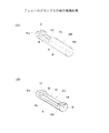
図1を参照すると、本発明の実施形態にかかる鍵型フェルールアセンブリ2Aの斜視図が示されている。鍵型フェルールアセンブリ2Aは、貫通孔6を有するフェルール4と、貫通孔6中に挿入固定されたベア光ファイバ8を含んでいる。フェルール4は例えばジリコニアから形成されている。
【0040】
フェルール4は第1端部4aと、第2端部4bと、第1及び第2端部4a,4bの間の中間部分4cを有しており、中間部分4cに貫通孔6中に挿入された光ファイバ8が半分露出するような切欠平坦部10を有している。
【0041】
フェルール4の一部を切り欠いた切欠平坦部10を先ず形成し、この状態で貫通孔6中にベア光ファイバ8を挿入し、ベア光ファイバ8の両端面をフェルール4の両端面とほぼ一致するように形成する。ベア光ファイバ8は、切欠平坦部10を除いた貫通孔6中でフェルール4に接着固定される。
【0042】
即ち、本実施形態の鍵型フェルールアセンブリ2Aでは、ベア光ファイバ8はフェルール4の両端部4a,4bにおいてその全周でフェルール4により保持されている。
【0043】
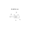
図2(A)は他の実施形態の鍵型フェルールアセンブリ2Bの斜視図を示している。鍵型フェルールアセンブリ2Bは第1端部4aに切削加工部12を有している。
【0044】
図2(B)は更に他の実施形態の鍵型フェルールアセンブリ2Cを示している。本実施形態では、切欠平坦部10の長さを大きく取り、両端部4a,4bに切削加工部12,14を形成している。
【0045】
図3(A)を参照すると、更に他の実施形態の鍵型フェルールアセンブリ2Dが示されている。本実施形態は、フェルール4の端部に切欠平坦部10を形成し、V溝18を有する押さえ部品16をフェルール4の端部の切欠平坦部10に接着するようにしたものである。
【0046】
本実施形態においても、光ファイバ8は両端部においてその全周がフェルール4及び押さえ部品16により保持されている。
【0047】
図3(B)は更に他の実施形態の鍵型フェルールアセンブリ2Eを示している。本実施形態では、ベア光ファイバ8をフェルール4の端部から突出させ、貫通孔22を有するビーズ部品20をフェルール4の端面に接着したものである。ベア光ファイバ8がビーズ部品20の貫通孔22中に挿入され、接着固定されている。
【0048】
図4を参照すると、更に他の実施形態の鍵型フェルールアセンブリ2Fが示されている。本実施形態は、第1実施形態の鍵型フェルールアセンブリ2Aの切欠平坦部10に貫通孔6に直交する段溝24を形成したものである。
【0049】
ベア光ファイバ8はフェルール4の貫通孔6中に挿入されて、接着剤で固定される。このとき貫通孔6中から押し出された接着剤は段溝24で受けられるため、接着剤10が切欠平坦部10に付着することが防止される。
【0050】
図5を参照すると、本発明実施形態のブロック型フェルールアセンブリ26の斜視図が示されている。ブロック型フェルールアセンブリ26は複数本の貫通孔30を有するブロック28を含んでいる。
【0051】
ブロック28は貫通孔30中に挿入されたベア光ファイバ32が半分露出するような切欠平坦部34を有している。切欠平坦部34を有するブロック28は、鋳型を用いてプラスチックのトランスファーモールドにより形成される。
【0052】
ブロック28は第1端部28a,第2端部28bを有しており、光ファイバ32が第1及び第2端部28a,28bでその全周でブロック28により保持されている。一対のガイドピン36がブロック28に挿入固定されている。
【0053】
光ファイバ32が第1及び第2端部28a,28bでブロック28により保持されているため、光ファイバ32の端面研磨加工が可能である。
【0054】
図6を参照すると、本発明第1実施形態の光モジュール40の分解斜視図が示されている。図7は、光モジュール40の斜視図であり、図8はその側面図を示している。光モジュール40はPLC(平面光導波回路)42と鍵型フェルールアセンブリ2Bとから構成される。
【0055】
PLC42はシリコン基板44上に形成された光導波構造46を有している。光導波構造46は光導波路コア部48と該光導波路コア部48を覆った光導波路クラッド部50を含んでいる。光導波路コア部48はその断面の一辺が約8μmの矩形をしており、光信号は屈折率が高い光導波路コア部48を伝搬する。
【0056】
シリコン基板44の一端部では基板表面44aが露出しており、V溝52がシリコンの異方性エッチングにより形成されている。直径125μmの円形断面を有するベア光ファイバがV溝52中に搭載されたとき、ベア光ファイバのコア部(直径9.5μm)の中心と光導波路コア部48の中心が一致するように、V溝52の位置と寸法が選ばれている。
【0057】
V溝52に直交して断面矩形状の溝54がダイシングソーによりシリコン基板44を切削することにより形成されている。溝54の幅は約320μm、深さは約300μmである。
【0058】
シリコンの異方性エッチングによりV溝52を形成するときに、V溝52の長手方向の一端部にも斜面が形成されるが、ダイシングソーで機械的にシリコン基板44を切削して溝54を形成することにより、V溝52内に搭載される光ファイバ8を光導波路コア部48に突き当てることができる。
【0059】
鍵型フェルールアセンブリ2Bは図2(A)を参照して説明したように、貫通孔6を有するフェルール4と、貫通孔6中に挿入され固定されたベア光ファイバ8を含んでいる。フェルール4は更に、貫通孔6中に挿入固定された光ファイバ8が半分露出するような切欠平坦部10を有している。
【0060】
フェルール4の一端部4aで光ファイバ8はその全周でフェルール4により保持されている。更に、一端部4aには切削加工部12が形成されている。切削加工部12は、軸方向の長さ約300μm、切欠平坦部10からの高さ約250μmの寸法を有している。このため、切削加工部12はPLC42の溝54に十分な余裕を持って嵌り、ベア光ファイバ8による位置合わせを阻害することはない。
【0061】
光モジュール40を組み立てるには、鍵型フェルールアセンブリ2Bを反転して、ベア光ファイバ8の一端が光導波路コア部48の一端に突き当てられるように、フェルール4の切削加工部12を溝54中に挿入するとともにベア光ファイバ8をV溝52中に挿入し、鍵型フェルールアセンブリ2Bを切欠平坦部10でシリコン基板44に接着する。
【0062】
図9を参照すると、本発明第2実施形態の光モジュール56の平面図が示されている。PLC42Aは3つの光導波路58a,58b,58cからなるY分岐光導波構造58を有している。
【0063】
基板44の左端には光導波路58a,58bの端部に整列したV形状のガイド溝60,62がシリコンの異方性エッチングにより形成されている。更に、溝64がダイシングソーにより形成されている。
【0064】
基板44の右端部には光導波路58cの端部に整列したV形状のガイド溝66がシリコンの異方性エッチングにより形成されており、ガイド溝66に直交する溝68がダイシングソーにより形成されている。
【0065】
各ガイド溝60,62,66中に光ファイバが搭載されるように3つの鍵型フェルールアセンブリ2BがPLC42Aに搭載される。
【0066】
図10を参照すると、本発明第3実施形態の光モジュール70の平面図が示されている。ウエットエッチング技術によりシリコン基板72にV形状のガイド溝74を形成するのと同じ工程で光素子78の位置合わせ用のマーカーを形成する。ガイド溝74に直交する溝76をダイシングソーにより形成する。
【0067】
更に、基板72上に銅又はアルミニウム等の金属を蒸着し、フォトリソグラフィにより所望形状にパターニングして電極を形成する。基板72のマーカーと光素子のマーカーを合せて光素子78を電極上にボンディングする。
【0068】
基板72のマーカーとガイド溝74は正確に位置関係が決定されているため、溝74に鍵型フェルールアセンブリ2Bの光ファイバが挿入されるように、鍵型フェルールアセンブリ2Bを基板72に搭載することにより、光素子78の受/発光部と鍵型フェルールアセンブリ2Bの光ファイバ8のコアとを高い精度で光結合させることが可能である。
【0069】
図11を参照すると、本発明第4実施形態の光モジュール80の平面図が示されている。本実施形態の光モジュール80では、図9に示した第2実施形態の光モジュール56と同様に、基板44上にY分岐光導波構造58、ガイド溝60,62及びガイド溝60,62に直交する溝64が形成されている。
【0070】
基板44上には、光導波路58cに光結合するようにフォトダイオード(PD)等の光素子78が搭載されている。更に、波長フィルタ82がY分岐光導波構造58の分岐部において、基板44に形成された溝にほぼ垂直に挿入固定されている。
【0071】
ガイド溝60,62中に各光ファイバが挿入されるように、2個の鍵型フェルールアセンブリ2Bが基板44に搭載されている。
【0072】
光素子78がPDであり、光信号が上側の鍵型フェルールアセンブリ2Bから光導波路58aに入射したとする。波長フィルタ82を透過する光はPD78により検出され、波長フィルタ82で反射された光は光導波路58bを介して下側の鍵型フェルールアセンブリ2Bに結合される。
【0073】
一方、光素子78が発光素子の場合には、発光素子78からの光は波長フィルタ82を透過してからY分岐で分岐され、光導波路58a,58bを伝搬して2つの鍵型フェルールアセンブリ2Bに結合される。
【0074】
図12を参照すると、本発明第5実施形態の光モジュール84の平面図が示されている。本実施形態の光モジュール84は、図18に示した構造を有する鍵型フェルールアセンブリ2Gにより、図7に示したPLC42と図10に示した光素子78を搭載した基板72を接続したものである。
【0075】
図18を参照して、鍵型フェルールアセンブリ2Gの構造に付いて説明する。鍵型フェルールアセンブリ2Gは貫通孔6を有するフェルール4と、貫通孔6中に挿入固定されたベア光ファイバ8を含んでいる。
【0076】
フェルール4は第1端部4aと、第2端部4bと、第1及び第2端部4a,4bの間の中間部分4cを有しており、光ファイバ8は第1及び第2端部4a,4b及び中間部分4cの貫通孔6中に挿入されて固定されている。
【0077】
第1及び第2端部4a,4bと中間部分4cとの間には貫通孔6中に挿入された光ファイバ8が半分露出するような切欠平坦部10a,10bがそれぞれ形成されている。
【0078】
本実施形態の光モジュール84は、上述した構造を有する鍵型フェルールアセンブリ2Gを使用するため、基板72上に搭載した光素子78とPLC42とを効率良く光結合することができる。更に、光モジュール84の組み立て作業性に優れている。
【0079】
図13を参照すると、本発明第6実施形態の光モジュール86の平面図が示されている。PLC42Cは図11に示したPLC42Bに類似しており、PLC42Bに搭載した光素子78に代わって基板44の右端部にV形状のガイド溝66と、ガイド溝66に直交する溝68を形成したものである。
【0080】
基板88は基板72に類似しており、V形状のガイド溝90と、ガイド溝90に直交する溝92を有している。基板88上にはレーザダイオード(LD)等の発光素子94が搭載されている。一方、基板72上にはPD等の受光素子78が搭載されている。
【0081】
基板88上に搭載された発光素子94とPLC42Cの光導波路58aは鍵型フェルールアセンブリ2Gにより光結合される。基板72上に搭載された受光素子78とPLC42Cの光導波路58cは鍵型フェルールアセンブリ2Gにより光結合される。PLC42Cの光導波路58bは鍵型フェルールアセンブリ2Bに光学的に接続されている。
【0082】
発光素子94から出射された光は鍵型フェルールアセンブリ2Gを介してPLC42Cの光導波路58aに結合する。光フィルタ82を透過する成分は光導波路58c、鍵型フェルールアセンブリ2Gを介して受光素子78に結合する。一方、光フィルタ82で反射された成分は光導波路58bを伝搬して鍵型フェルールアセンブリ2Bに結合される。
【0083】
図14を参照すると、本発明第7実施形態の光モジュール96の平面図が示されている。本実施形態の光モジュール96は、PLC基板44の両端に直径の異なる鍵型フェルールアセンブリ2B、2Hを搭載したピッチ変換機能を有する光モジュールである。PLC42Dは2つの光導波路98,100を有している。
【0084】
光導波路98,100の両端にそれぞれ2つのガイド溝を形成し、一端部のガイド溝には直径2.5mmの鍵型フェルールアセンブリ2Bを搭載し、他端のガイド溝には直径1.25mmの鍵型フェルールアセンブリ2Hを搭載する。
【0085】
本実施形態の光モジュール96は図示された構造に限定されるものではなく、フェルールアセンブリの数は基板44に形成された光導波路の数に応じて決定される。
【0086】
また、光導波路に分岐機能を持たせることで、基板44の左右に搭載する鍵型フェルールアセンブリの数が異なっていても良い。更に、基板44上に光素子、光フィルタ等が搭載されていても良い。
【0087】
図15を参照すると、本発明第8実施形態の光モジュール102の分解斜視図が示されている。図16は光モジュール102の斜視図、図17はその側面図である。本実施形態の光モジュール102は、PLC42Eと、鍵型フェルールアセンブリ2Bと、ガラス板106から構成される。
【0088】
PLC42Eの光導波構造46はクラッド層50の一部を除去した幅の狭い部分46aを有しており、光導波路コア部48はシリコン基板長手方向全長に渡り伸長している。
【0089】
光導波構造46の幅が狭い部分46aの両側ではシリコン基板44の表面が露出しており、ガラス板106と位置合わせを行うための一対のマーカー溝104がエッチングにより形成されている。
【0090】
ガラス板106はその片面に幅の狭い光導波構造46aを収容する溝108と、V溝110と、V溝110に直交するように溝108とV溝110との間に形成された断面矩形状の溝112を有している。
【0091】
ガラス板106は更に、PLC42Eとの位置合わせ用の一対のマーカー溝114を有している。溝108、V溝110、溝112及びマーカー溝114は切削又はガラスモールド等により形成される。
【0092】
ガラス板106とPLC42Eは、幅の狭い光導波構造部分46aを溝108中に収容してPLC42Eのマーカー溝104とガラス板106のマーカー溝114が一致するように接着固定される。
【0093】
一方、ガラス板106と鍵型フェルールアセンブリ2Bは、フェルール4の切削加工部12をガラス板106の溝112中に収容し、ベア光ファイバ8がV溝110に嵌合することによって、自己整合的に位置合わせされて接着固定される。
【0094】
鍵型フェルールアセンブリ2Bの切欠平坦部10とガラス板106の下面との間には約10μm程度のギャップがあり、このギャップ中に接着剤が充填されてガラス板106と鍵型フェルールアセンブリ2Bが接着固定される。
【0095】
V溝110の形状、寸法及びマーカー溝104,114との相対位置は、光導波路コア部48の中心とベア光ファイバ8のコアの中心が一致するように選択される。
【0096】
本実施形態によれば、PLC42EにV溝を形成しなくても、V溝110付きのガラス板106を介して鍵型フェルールアセンブリ2BをPLC42Eに接続することによって、低損失の光接続を低コストで実現することができる。
【0097】
図18を参照すると、本発明第9実施形態の光モジュール116の分解斜視図が示されている。図19は光モジュール116の斜視図であり、図20はその側面図である。
【0098】
本実施形態の光モジュール116は、2つの切欠平坦部10a,10bを有する鍵型フェルールアセンブリ2Gによって、同一構造のPLC42と42´を光学的に接続したものである。
【0099】
図21を参照すると、本発明第10実施形態の光モジュール118の組み立て前の分解斜視図が示されている。図22は組み立て後の光モジュール118の斜視図を示している。
【0100】
本実施形態は、両端に複数のV溝120,124を有するPLC42Fを介して、2個のブロック型フェルールアセンブリ26A,26Bを光学的に結合した実施形態である。
【0101】
PLC42Fの光導波構造46は複数のY分岐型光導波路コア部48を有している。基板44の一端部には光導波路コア部48に整列して2個のV溝120がエッチングにより形成され、V溝120に直交する溝122がダイシングソーにより形成されている。
【0102】
基板44の他端部には多数に分岐した光導波路コア部48に整列して多数のV溝124がエッチングにより形成され、V溝124に直交する溝126がダイシングソーにより形成されている。
【0103】
ブロック型フェルールアセンブリ26A,26Bは図5に示したブロック型フェルールアセンブリ26に類似しており、各光ファイバ32の一端を押さえ部材128で押さえている点が相違する。
【0104】
ブロック型フェルールアセンブリ26Aは2本の光ファイバ32を有しており、ブロック型フェルールアセンブリ26BはV溝124に対応した数の光ファイバ32を有している。130は接着剤滴下穴である。
【0105】
本実施形態の光モジュール118では、ブロック型フェルールアセンブリ26Aから入力された光信号は複数に分岐されてブロック型フェルールアセンブリ26Bから出力される。逆に、ブロック型フェルールアセンブリ26Bから入力された光信号はPLC42Fで合波されて、ブロック型フェルールアセンブリ26Aから出力される。
【0106】
図23を参照すると、本発明第11実施形態の光モジュール131の組み立て前の分解斜視図が示されている。図24は光モジュール131の組み立て後の斜視図である。
【0107】
ブロック型フェルールアセンブリ144は複数の貫通孔148を有するブロック146と、各貫通孔148中に挿入固定された複数のベア光ファイバ150を含んでいる。
【0108】
各ベア光ファイバ150はその両端においてブロック146と一体的に形成されたファイバ保持部154a,154bで保持されている。ブロック146には貫通孔148中に挿入固定された光ファイバ150が半分露出する2個の切欠平坦部152a,152bが形成されている。
【0109】
PLC42GにはY分岐した光導波路コア部10に整列した複数のV溝132と、V溝132に直交する溝134が形成されている。
【0110】
基板136は複数のV溝138と、V溝138に直交する溝140を有している。V溝138に整列して複数の光素子78が搭載されている。符号142は接着剤逃し用の溝である。
【0111】
ブロック型フェルールアセンブリ144の一方の切欠平坦部152aに、光ファイバ150がPLC42GのV溝132に嵌合されるように、PLC42Gが接着固定される。
【0112】
更に、ブロック型フェルールアセンブリ144の他方の切欠平坦部152bに光ファイバ150が基板136のV溝138に嵌合されるように、基板136が接着固定される。
【0113】
本実施形態によると、ブロック型フェルールアセンブリ144を介して基板136上に搭載された光素子78と、PLC42Gが光学的に結合される。
【0114】
本発明は以下の付記を含むものである。
【0115】
(付記1) フェルールアセンブリであって、
貫通孔と、第1端部と、該第1端部の反対側の第2端部と、該第1及び第2端部の間の中間部分を有するフェルールと;
前記貫通孔中に挿入されて固定された光ファイバとを具備し;
前記フェルールは前記貫通孔中に挿入された光ファイバが半分露出するような切欠平坦部を前記中間部分に有しており、前記光ファイバは前記フェルールの少なくとも前記第1及び第2端部においてその全周を該フェルールにより保持されていることを特徴とするフェルールアセンブリ。
【0116】
(付記2) 前記フェルールは前記第1端部に切削加工部を有している付記1記載のフェルールアセンブリ。
【0117】
(付記3) 前記フェルールは前記第1端部及び第2端部にそれぞれ切削加工部を有している付記1記載のフェルールアセンブリ。
【0118】
(付記4) フェルールアセンブリであって、
貫通孔と切欠平坦部を有するフェルールと;
前記貫通孔中に挿入固定され、前記切欠平坦部で半分露出した光ファイバと;
前記切欠平坦部に接着されて半分露出した光ファイバを押さえる押さえ部材と;
を具備したことを特徴とするフェルールアセンブリ。
【0119】
(付記5) ブロック型フェルールアセンブリであって、
貫通孔と、第1端部と、該第1端部の反対側の第2端部と、該第1及び第2端部の間の中間部分を有するブロックと;
前記貫通孔中に挿入されて固定された光ファイバと;
前記ブロックの前記第1端部に固定された複数のガイドピンとを具備し;
前記ブロックは前記貫通孔中に挿入された光ファイバが半分露出するような切欠平坦部を前記中間部分に有しており、前記光ファイバは前記ブロックの前記第1及び第2端部においてその全周を該ブロックにより保持されていることを特徴とするブロック型フェルールアセンブリ。
【0120】
(付記6) 光モジュールであって、
第1の溝と該第1の溝に直交する第2の溝を有する基板と;
一端が前記第1の溝の一端に整列した光導波路コア部と該光導波路コア部を覆った光導波路クラッド部とを有する、前記基板上に形成された光導波構造と;
貫通孔と、第1端部と、該第1端部の反対側の第2端部と、該第1及び第2端部の間の中間部分を有するフェルールと;
前記貫通孔中に挿入されて固定された光ファイバとを具備し;
前記フェルールは前記貫通孔中に挿入された光ファイバが半分露出するような切欠平坦部を前記中間部分に有し、前記光ファイバは前記フェルールの少なくとも前記第1及び第2端部においてその全周を該フェルールにより保持されており;
前記フェルールの前記第1端部が前記第2の溝中に挿入され、前記光ファイバの一端が前記光導波路コア部の一端に突き当てられるように前記光ファイバが前記基板の第1の溝中に挿入されて、前記フェルールが前記切欠平坦部で前記基板に固定されていることを特徴とする光モジュール。
【0121】
(付記7) 前記光導波路コア部の他端に光結合するように前記基板上に搭載された光素子を更に具備した付記6記載の光モジュール。
【0122】
(付記8) 光モジュールであって、
第1の溝と、該第1の溝に直交する第2の溝を有する基板と;
前記第1の溝に整列して前記基板上に搭載された光素子と;
貫通孔と、第1端部と、該第1端部の反対側の第2端部と、該第1及び第2端部の間の中間部分を有するフェルールと;
前記貫通孔中に挿入されて固定された光ファイバとを具備し;
前記フェルールは前記貫通孔中に挿入された光ファイバが半分露出するような切欠平坦部を前記中間部分に有し、前記光ファイバは前記フェルールの少なくとも前記第1及び第2端部においてその全周を該フェルールにより保持されており;
前記フェルールの前記第1端部は前記第2の溝中に挿入され、前記光ファイバの一端が前記光素子に光結合するように前記光ファイバが前記基板の第1の溝中に挿入されて、前記フェルールが前記切欠平坦部で前記基板に固定されていることを特徴とする光モジュール。
【0123】
(付記9) 光モジュールであって、
第1の溝と該第1の溝に直交する第2の溝を有する第1基板と;
第3の溝と該第3の溝に直交する第4の溝を有する第2基板と;
一端が前記第1の溝の一端に整列した第1光導波路コア部と該第1光導波路コア部を覆った第1光導波路クラッド部とを有する、前記第1基板上に形成された第1光導波構造と;
一端が前記第3の溝の一端に整列した第2光導波路コア部と該第2光導波路コア部を覆った第2光導波路クラッド部とを有する、前記第2基板上に形成された第2光導波構造と;
貫通孔と、第1端部と、該第1端部の反対側の第2端部とを有するフェルールと;
前記貫通孔中に挿入されて固定された光ファイバとを具備し;
前記フェルールは前記貫通孔中に挿入された光ファイバが半分露出するような第1及び第2切欠平坦部を有し、前記光ファイバは前記フェルールの少なくとも前記第1及び第2端部においてその全周を該フェルールにより保持されており;
前記フェルールの前記第1端部が前記第1基板の前記第2の溝中に挿入され、第2端部が前記第2基板の前記第4の溝中に挿入され、前記光ファイバの一端が前記第1光導波路コア部の一端に突き当てられ、他端が前記第2光導波路コア部の一端に突き当てられるように、前記光ファイバが前記第1及び第2基板の前記第1及び第3の溝中に挿入されて、前記フェルールが前記第1及び第2切欠平坦部で前記第1及び第2基板にそれぞれ固定されていることを特徴とする光モジュール。
【0124】
(付記10) 光モジュールであって、
第1の溝と該第1の溝に直交する第2の溝を有する第1基板と;
第3の溝と該第3の溝に直交する第4の溝を有する第2基板と;
一端が前記第1の溝の一端に整列した光導波路コア部と該光導波路コア部を覆った光導波路クラッド部とを有する、前記第1基板上に形成された光導波構造と;
前記第3の溝に整列して前記第2基板上に搭載された光素子と;
貫通孔と、第1端部と、該第1端部の反対側の第2端部を有するフェルールと;
前記貫通孔中に挿入されて固定された光ファイバとを具備し;
前記フェルールは前記貫通孔中に挿入された光ファイバが半分露出するような第1及び第2切欠平坦部を有し、前記光ファイバは前記フェルールの少なくとも前記第1及び第2端部においてその全周を該フェルールにより保持されており;
前記フェルールの第1及び第2端部が前記第2及び第4の溝中にそれぞれ挿入され、前記光ファイバの一端が前記光導波路コア部の一端に突き当てられ、他端が前記光素子に光結合するように前記光ファイバが前記第1及び第2基板の前記第1及び第3の溝中にそれぞれ挿入されて、前記フェルールが前記第1及び第2切欠平坦部で前記第1及び第2基板にそれぞれ固定されていることを特徴とする光モジュール。
【0125】
(付記11) 光モジュールであって、
表面上に第1マーカーの形成された基板と;
光導波路コア部と該光導波路コア部を覆った幅の狭い第1部分と幅の広い第2部分とを有する光導波路クラッド部とを含んだ、前記基板上に形成された光導波構造と;
幅の広い第1の溝と、幅の狭い第2の溝と、該第1及び第2の溝に直交するように該第1及び第2の溝の間に形成された第3の溝と、第2マーカーとを有し、該第2マーカーが前記第1マーカーに位置合わせされて前記第1の溝が前記光導波路クラッド部の前記第1部分を収容するように前記基板上に固定されたガラス板と;
貫通孔と、第1端部と、第2端部と、該第1及び第2端部の間の中間部分を有するフェルールと、前記貫通孔中に挿入されて固定された光ファイバとを含み、前記フェルールは前記貫通孔中に挿入された光ファイバが半分露出するような切欠平坦部を前記中間部分に有し、前記光ファイバは前記フェルールの少なくとも前記第1及び第2端部においてその全周を該フェルールにより保持されており、前記フェルールの前記第1端部が前記ガラス板の前記第3の溝中に挿入され、前記光ファイバが前記第2の溝中に挿入されて、前記切欠平坦部で前記ガラス板に固定されたフェルールアセンブリと;
を具備したことを特徴とする光モジュール。
【0126】
(付記12) 光モジュールであって、
一端部に形成された第1の溝と、該第1の溝に直交する第2の溝と、他端部に形成された複数の第3の溝と、該第3の溝に直交する第4の溝を有する基板と;
一端部が前記第1の溝の一端部に整列し、他端部が複数に分岐されてそれぞれ前記複数の第3の溝の一端部に整列した光導波路コア部と、該光導波路コア部を覆った光導波路クラッドとを有する、前記基板上に形成された光導波構造と;
第1貫通孔と、第1端部と、第2端部とを有する第1ブロックと、前記第1貫通孔中に挿入されて固定された第1光ファイバと、前記第1ブロックに固定された複数の第1ガイドピンとを含み、前記第1ブロックは前記第1貫通孔中に挿入された前記第1光ファイバが半分露出するような第1切欠平坦部を有し、前記第1光ファイバは前記第1ブロックの少なくとも前記第1及び第2端部においてその全周を前記第1ブロックにより保持されている第1ブロック型フェルールアセンブリと;
複数の第2貫通孔と、第3端部と、第4端部とを有する第2ブロックと、前記各第2貫通孔中に挿入されて固定された複数の第2光ファイバと、前記第2ブロックに固定された複数の第2ガイドピンとを含み、前記第2ブロックは前記各第2貫通孔中に挿入された前記各第2光ファイバが半分露出するような第2切欠平坦部を有し、前記各第2光ファイバは前記第2ブロックの少なくとも前記第3及び第4端部においてその全周を前記第2ブロックにより保持されている第2ブロック型フェルールアセンブリとを具備し;
前記第1光ファイバの一端が前記光導波路コア部の前記一端部に突き当てられるように前記第1光ファイバが前記基板の第1の溝中に挿入されて、前記第1ブロック型フェルールアセンブリが前記第1切欠平坦部で前記基板に固定されており、
前記複数の第2光ファイバの一端が前記光導波路コア部の複数に分岐した前記各他端部に突き当てられるように前記複数の第2光ファイバが前記基板の前記複数の第3の溝中にそれぞれ挿入されて、前記第2ブロック型フェルールアセンブリが前記第2切欠平坦部で前記基板に固定されていることを特徴とする光モジュール。
【0127】
(付記13) 光モジュールであって、
第1の溝と、該第1の溝に直交する第2の溝を有する第1基板と;
一端が前記第1の溝の一端に整列した光導波路コア部と該光導波路コア部を覆った光導波路クラッド部とを有する、前記第1基板上に形成された光導波構造と;
第3の溝と、該第3の溝に直交する第4の溝を有する第2基板と;
前記第3の溝に整列して前記第2基板上に搭載された光素子と;
貫通孔と、第1切欠平坦部と、該第1切欠平坦部と離間した第2切欠平坦部とを有するブロックと、前記貫通孔中に挿入されて固定された光ファイバとを含み、前記ブロックは前記光ファイバをその全周で保持する第1及び第2保持部を第1及び第2端部に有しており、前記光ファイバは前記第1及び第2切欠平坦部で半分露出しているブロック型フェルールアセンブリとを具備し;
前記ブロックの前記第1保持部が前記第1基板の第2の溝中に挿入され、前記光ファイバが前記第1の溝中に挿入されて、前記第1基板が前記ブロック型フェルールアセンブリに固定されており;
前記ブロックの前記第2保持部が前記第2基板の第4の溝中に挿入され、前記光ファイバが前記第3の溝中に挿入されて、前記第2基板が前記ブロック型フェルールアセンブリに固定されていることを特徴とする光モジュール。
【0128】
【発明の効果】
本発明によれば、光ファイバとのインタフェース部に鍵型フェルールアセンブリを使用することにより、低コスト化、小型化に適したレセプタクル型光モジュールを提供することができる。
【図面の簡単な説明】
【図1】本発明実施形態の鍵型フェルールアセンブリの斜視図である。
【図2】図2(A)は本発明の他の実施形態の鍵型フェルールアセンブリの斜視図であり、図2(B)は更に他の実施形態の鍵型フェルールアセンブリの斜視図である。
【図3】図3(A)は本発明の更に他の実施形態の鍵型フェルールアセンブリの分解斜視図であり、図3(B)は更に他の実施形態の鍵型フェルールアセンブリの分解斜視図である。
【図4】本発明の更に他の実施形態の鍵型フェルールアセンブリの斜視図である。
【図5】本発明実施形態のブロック型フェルールアセンブリの斜視図である。
【図6】本発明第1実施形態の光モジュールの組み立て前の分解斜視図である。
【図7】第1実施形態の光モジュールの組み立て後の斜視図である。
【図8】第1実施形態の光モジュールの側面図である。
【図9】本発明第2実施形態の光モジュールの平面図である。
【図10】本発明第3実施形態の光モジュールの平面図である。
【図11】本発明第4実施形態の光モジュールの平面図である。
【図12】本発明第5実施形態の光モジュールの平面図である。
【図13】本発明第6実施形態の光モジュールの平面図である。
【図14】本発明第7実施形態の光モジュールの平面図である。
【図15】本発明第8実施形態の光モジュールの組み立て前の分解斜視図である。
【図16】第8実施形態の光モジュールの組み立て後の斜視図である。
【図17】第8実施形態の光モジュールの側面図である。
【図18】本発明第9実施形態の光モジュールの組み立て前の分解斜視図である。
【図19】第9実施形態の光モジュールの組み立て後の斜視図である。
【図20】第9実施形態の光モジュールの側面図である。
【図21】本発明第10実施形態の光モジュールの組み立て前の分解斜視図である。
【図22】第10実施形態の光モジュールの組み立て後の斜視図である。
【図23】本発明第11実施形態の光モジュールの組み立て前の斜視図である。
【図24】第11実施形態の光モジュールの組み立て後の斜視図である。
【符号の説明】
2A〜2G 鍵型フェルールアセンブリ
4 フェルール
6 貫通孔
8 ベア光ファイバ
10 切欠平坦部
12,14 切削加工部
26 ブロック型フェルールアセンブリ
42 PLC
44 シリコン基板
46 光導波構造
48 光導波路コア部
52 V溝
54 溝
104,114 マーカー溝
106 ガラス板[0001]
BACKGROUND OF THE INVENTION
The present invention relates to a ferrule assembly that incorporates an optical fiber and connects to an optical component, and more particularly to a receptacle-type optical transmission module that uses the ferrule assembly.
[0002]
In the information and communication field in recent years, it has become necessary to transmit a large amount of information at a high speed as the amount of information increases. Currently, high-speed and large-capacity optical communication networks such as optical subscriber lines are being widely used. ing. In order to popularize optical subscriber systems, it is inevitable to reduce the cost of optical modules.
[0003]
The price of an optical module is composed of component costs, assembly costs, testing and adjustment costs, and especially the assembly costs and adjustment costs occupy a large part. In recent years, receptacle-type optical modules have been spotlighted as means for reducing assembly costs.
[0004]
[Prior art]
Components mounted on a printed wiring board incorporated in a communication device are generally classified into a surface mounting type and a through hole mounting type. A typical example of the surface-mounted component is an LSI, which has a shape called a flat package type.
[0005]
This component is soldered by a method called reflow soldering. That is, paste-like solder is printed on a printed wiring board, surface-mounted components are adhered to the paste solder portion, and soldering is performed in a conveyor furnace where the solder surface temperature is 220 ° C. or higher.
[0006]
Typical examples of through-hole mounting type components are large-capacity capacitors and LSIs with a large number of terminals (200 terminals or more). An LSI with a large number of terminals has a terminal form called PGA (Pin Grid Array).
[0007]
These through-hole mounted components are soldered by a method called flow soldering. That is, the terminal of the through-hole mounting type component is inserted into the through hole of the printed wiring board, and the printed wiring board is put into a solder bath at about 260 ° C. from the side opposite to the component mounting surface, and soldering is performed.
[0008]
By the way, in order to mount an optical module on a printed wiring board by a soldering process in the same manner as a surface-mounted component or a through-hole mounted component, a so-called pigtail-type optical module with an optical fiber cord is not suitable.
[0009]
Usually, the optical fiber cord has a nylon coating, and the nylon coating has a heat resistance of only about 80 ° C., and therefore melts in the soldering process. In addition, the optical fiber cord itself causes a housing and handling problem at the manufacturing site, and the mounting efficiency on the printed wiring board is remarkably reduced.
[0010]
For this reason, in order to enable the soldering process of the optical module and reduce the manufacturing cost, it is indispensable to provide a so-called receptacle type optical module that does not include an optical fiber cord.
[0011]
In the receptacle type optical module, a connector portion is provided on the optical module, and a coated optical fiber cord that is weak against heat is detachable. In the receptacle-type optical module, a high-temperature solder reflow process can be applied, and the optical module can be mounted on the printed wiring board simultaneously with the surface-mount type electronic component.
[0012]
By simultaneously mounting the optical component and the electronic component on the printed wiring board, it is possible to simplify a plurality of mounting processes using solder having different melting points, which has been required in the past, and a significant cost reduction can be expected.
[0013]
Self-alignment techniques are being studied as a means for reducing adjustment costs. This is because optical guides (optical fibers, ferrules, etc.) are mounted along the guide by forming a guide part that defines the positional relationship with the optical component with high precision on the optical component mounting substrate. Is what you do. Self-alignment technology makes it possible to omit an alignment process that requires large man-hours and costs.
[0014]
JP 11-26492
[0015]
In the optical module disclosed in Japanese Patent Application Laid-Open No. 7-318764, as another form for performing self-alignment, the bare optical fiber is projected from the ferrule end, and the optical fiber is inserted into the guide groove formed on the optical element mounting substrate. The method of fixing is proposed. This structure has a feature that a higher mounting accuracy can be obtained because the optical fiber can be directly aligned in the guide groove.
[0016]
As another prior art, JP-A-2000-171668 can be mentioned. In the optical module described in this publication, as another form for self-alignment, a part of the ferrule is cut out to expose half of the bare optical fiber, and is mounted in a guide groove provided on the optical element mounting substrate. A method of fixing is proposed.
[0017]
In the optical module having this structure, since a part of the ferrule is used for holding the bare optical fiber, not only the holding part can be omitted, but also the adhesion area can be reduced.
[0018]
[Problems to be solved by the invention]
The characteristics required for a low-cost and highly reliable receptacle-type optical module are: (1) easy mounting, (2) high strength, and (3) end face polishing and anti-reflection measures. (4) The positioning accuracy is high.
[0019]
In particular, end face polishing is highly anticipated as a means for preventing reflection. In order to reduce reflected return light, which has been a major issue in recent years, from the current level of about 25 dB to 40 dB or more in the future, an oblique polishing structure in which the fiber end face is inclined with respect to the optical axis is effective. It is. In order to realize this structure, it is necessary that the fiber end can be polished.
[0020]
The optical module described in the above-mentioned JP-A-11-264926 has the following problems. It is necessary to form a guide groove having a depth corresponding to the radius of the ferrule (about 650 μm in the case of a standard MU type ferrule), which increases the etching time and makes it difficult to form a protective film. Also, a large-sized optical component mounting substrate is required.
[0021]
A large guide groove has low controllability of width when formed, and an abnormal etching surface is likely to be formed on an inclined surface by long-time etching. Furthermore, since the alignment is performed using the outer shape of the ferrule, an optical coupling loss occurs due to the eccentricity of the inner diameter of the ferrule and the eccentricity when the optical fiber is inserted.
[0022]
The optical module disclosed in Japanese Patent Laid-Open No. 7-318764 has the following problems. It is impossible to polish the end face of the optical fiber. Further, since the optical fiber is completely exposed from the ferrule, there is a high risk of breakage during handling.
[0023]
Furthermore, since the optical fiber fixing part and the ferrule fixing part are independent in the optical module, stress is generated at the boundary between the optical fiber and the ferrule, which may adversely affect the reliability.
[0024]
The optical module disclosed in Japanese Patent Laid-Open No. 2000-171668 has the following problems. End face polishing is impossible due to the high risk of fiber breakage. Further, since the bare optical fiber cannot be fixed to the ferrule at the notch flat portion, there is a risk of damage to the optical fiber.
[0025]
Accordingly, an object of the present invention is to provide a receptacle-type optical module that is suitable for cost reduction and downsizing.
[0026]
Another object of the present invention is to provide a ferrule assembly required to assemble a receptacle type optical module.
[0027]
[Means for Solving the Problems]
According to the present invention, a ferrule assembly includes a through hole, a first end, a second end opposite the first end, and an intermediate portion between the first and second ends. A ferrule having an optical fiber inserted and fixed in the through hole; and the ferrule has a notch flat portion in the intermediate portion so that the optical fiber inserted in the through hole is half exposed. The optical fiber is held by the ferrule all around at least the first and second end portions of the ferrule. In addition, the entire length of the optical fiber is held in contact with the ferrule. A ferrule assembly is provided.
[0028]
Preferably, the ferrule has a cutting part at the first end and / or the second end.
[0029]
According to the ferrule assembly of the present invention, it is possible to realize all the above-described four requirement items that could not be satisfied by the prior art.
[0030]
(1) Since the optical fiber is fixed to the ferrule at both ends of the ferrule, it can be handled in the same manner as the standard MU ferrule, and is easy to mount.
[0031]
(2) Since the optical fibers are fixed to the ferrules at both ends of the ferrule, there is no risk of optical fiber breakage.
[0032]
(3) End face polishing of ferrules and optical fibers is possible.
[0033]
(4) Highly accurate self-alignment using a bare optical fiber is possible.
[0034]
According to another aspect of the present invention, a block-type ferrule assembly includes a through hole, a first end, a second end opposite to the first end, and the first and second ends. A block having an intermediate portion therebetween; an optical fiber inserted into and fixed to the through hole; and a plurality of guide pins fixed to the first end of the block; The intermediate portion has a notch flat portion that exposes half of the optical fiber inserted into the hole, and the optical fiber has its entire circumference at the first and second ends of the block by the block. Retained In addition, the entire length of the optical fiber is held in contact with the block. A block-type ferrule assembly is provided.
[0035]
According to still another aspect of the present invention, an optical module comprising a first groove and a substrate having a second groove perpendicular to the first groove; one end aligned with one end of the first groove An optical waveguide structure formed on the substrate, having an optical waveguide core portion and an optical waveguide cladding portion covering the optical waveguide core portion; a through hole, a first end portion, and the opposite of the first end portion A ferrule having a second end on the side and an intermediate portion between the first and second ends; and an optical fiber inserted and fixed in the through hole; The intermediate portion has a notch flat portion in which the optical fiber inserted therein is half exposed, and the optical fiber is held at its first and second ends by the ferrule at least at the first and second ends. The first end of the ferrule is the second The optical fiber is inserted into the first groove of the substrate so that one end of the optical fiber is abutted against one end of the optical waveguide core portion, and the ferrule is formed at the notch flat portion. An optical module is provided that is fixed to a substrate.
[0036]
According to still another aspect of the present invention, an optical module comprising a first substrate having a first groove and a second groove orthogonal to the first groove; a third groove and the third groove A second substrate having a fourth groove perpendicular to the first optical waveguide; a first optical waveguide core portion having one end aligned with one end of the first groove; and a first optical waveguide clad portion covering the first optical waveguide core portion; A first optical waveguide structure formed on the first substrate; a second optical waveguide core portion having one end aligned with one end of the third groove; and a second optical waveguide core portion covering the second optical waveguide core portion A second optical waveguide structure formed on the second substrate having an optical waveguide cladding; a through hole, a first end, and a second end opposite to the first end A ferrule; and an optical fiber inserted and fixed in the through hole; and the ferrule is an optical fiber inserted in the through hole. And the optical fiber is held by the ferrule at its first and second ends at least at the first and second ends of the ferrule; The first end is inserted into the second groove of the first substrate, the second end is inserted into the fourth groove of the second substrate, and one end of the optical fiber is the first groove The first and third grooves of the first and second substrates so that the optical fiber is abutted against one end of the optical waveguide core and the other end is abutted against one end of the second optical waveguide core. An optical module is provided, wherein the optical module is inserted into the ferrule and fixed to the first and second substrates at the first and second cutout flat portions, respectively.
[0037]
According to still another aspect of the present invention, there is provided an optical module, a substrate having a first marker formed on a surface thereof; an optical waveguide core portion, a narrow first portion covering the optical waveguide core portion, and a width An optical waveguide structure formed on the substrate including an optical waveguide clad portion having a wide second portion; a wide first groove; a narrow second groove; And a third groove formed between the first and second grooves so as to be orthogonal to the second groove, and a second marker, the second marker being aligned with the first marker A plate fixed on the substrate such that the first groove accommodates the first portion of the optical waveguide cladding; a through hole; a first end; a second end; A ferrule having an intermediate portion between the first and second ends, and an optical fiber inserted and fixed in the through hole The ferrule has a notch flat portion in the intermediate portion so that the optical fiber inserted into the through hole is half exposed, and the optical fiber is at least at the first and second ends of the ferrule. The entire circumference is held by the ferrule, and the first end of the ferrule is plate And a ferrule assembly that is inserted into the third groove and the optical fiber is inserted into the second groove and fixed to the plate at the notch flat portion. A module is provided.
[0038]
DETAILED DESCRIPTION OF THE INVENTION
Hereinafter, a number of embodiments of the present invention will be described in detail with reference to the drawings. In the description of each embodiment, substantially the same or similar components are denoted by the same reference numerals, and a part of the description is omitted to avoid duplication.
[0039]
Referring to FIG. 1, a key-type ferrule assembly 2 according to an embodiment of the present invention. A A perspective view is shown. The key-type ferrule assembly 2 </ b> A includes a
[0040]
The
[0041]
First, a notch
[0042]
That is, in the key
[0043]
FIG. 2A shows a perspective view of a key
[0044]
FIG. 2B shows a key-
[0045]
Referring to FIG. 3 (A), a key type ferrule assembly 2D of still another embodiment is shown. In this embodiment, the notched
[0046]
Also in this embodiment, the entire circumference of the
[0047]
FIG. 3B shows a key-
[0048]
Referring to FIG. 4, yet another embodiment of a key-
[0049]
The bare
[0050]
Referring to FIG. 5, a perspective view of the block
[0051]
The
[0052]
The
[0053]
Since the
[0054]
Referring to FIG. 6, an exploded perspective view of the
[0055]
The
[0056]
The
[0057]
A
[0058]
When forming the V-
[0059]
As described with reference to FIG. 2A, the key-type ferrule assembly 2 </ b> B includes the
[0060]
At one end 4 a of the
[0061]
To assemble the
[0062]
Referring to FIG. 9, a plan view of an
[0063]
At the left end of the
[0064]
At the right end of the
[0065]
Three key-
[0066]
Referring to FIG. 10, a plan view of an
[0067]
Further, a metal such as copper or aluminum is vapor-deposited on the
[0068]
Since the positional relationship between the marker of the
[0069]
Referring to FIG. 11, a plan view of an
[0070]
An
[0071]
Two key-
[0072]
It is assumed that the
[0073]
On the other hand, when the
[0074]
Referring to FIG. 12, a plan view of an
[0075]
The structure of the key
[0076]
The
[0077]
Notched
[0078]
Since the
[0079]
Referring to FIG. 13, a plan view of an
[0080]
The
[0081]
The
[0082]
The light emitted from the
[0083]
Referring to FIG. 14, a plan view of an
[0084]
Two guide grooves are formed at both ends of the
[0085]
The
[0086]
Further, the number of key-type ferrule assemblies mounted on the left and right of the
[0087]
Referring to FIG. 15, an exploded perspective view of the
[0088]
The
[0089]
The surface of the
[0090]
The
[0091]
The
[0092]
The
[0093]
On the other hand, the
[0094]
There is a gap of about 10 μm between the notch
[0095]
The shape and size of the
[0096]
According to the present embodiment, even if the V-groove is not formed in the
[0097]
Referring to FIG. 18, an exploded perspective view of the
[0098]
The
[0099]
Referring to FIG. 21, an exploded perspective view of the
[0100]
In the present embodiment, two block
[0101]
The
[0102]
At the other end of the
[0103]
The block
[0104]
The block
[0105]
In the
[0106]
Referring to FIG. 23, an exploded perspective view of the
[0107]
The block
[0108]
Each bare
[0109]
In the
[0110]
The
[0111]
The
[0112]
Further, the
[0113]
According to the present embodiment, the
[0114]
The present invention includes the following supplementary notes.
[0115]
(Appendix 1) Ferrule assembly,
A ferrule having a through hole, a first end, a second end opposite the first end, and an intermediate portion between the first and second ends;
An optical fiber inserted into and fixed to the through hole;
The ferrule has a notch flat portion in the intermediate portion so that the optical fiber inserted into the through hole is half exposed, and the optical fiber is at least at the first and second ends of the ferrule. A ferrule assembly, wherein the entire circumference is held by the ferrule.
[0116]
(Supplementary note 2) The ferrule assembly according to
[0117]
(Additional remark 3) The said ferrule is a ferrule assembly of
[0118]
(Appendix 4) A ferrule assembly,
A ferrule having a through hole and a notched flat portion;
An optical fiber inserted and fixed in the through hole and half exposed at the notch flat part;
A holding member for holding the half-exposed optical fiber bonded to the notch flat part;
A ferrule assembly comprising:
[0119]
(Additional remark 5) It is a block type ferrule assembly,
A block having a through hole, a first end, a second end opposite the first end, and an intermediate portion between the first and second ends;
An optical fiber inserted into the through hole and fixed;
A plurality of guide pins fixed to the first end of the block;
The block has a notch flat portion in the intermediate portion so that half of the optical fiber inserted into the through-hole is exposed, and the optical fiber is entirely at the first and second ends of the block. A block-type ferrule assembly having a periphery held by the block.
[0120]
(Appendix 6) An optical module,
A substrate having a first groove and a second groove orthogonal to the first groove;
An optical waveguide structure formed on the substrate, the optical waveguide core having one end aligned with one end of the first groove, and an optical waveguide cladding covering the optical waveguide core;
A ferrule having a through hole, a first end, a second end opposite the first end, and an intermediate portion between the first and second ends;
An optical fiber inserted into and fixed to the through hole;
The ferrule has a cutout flat portion at the intermediate portion so that the optical fiber inserted into the through hole is half exposed, and the optical fiber has an entire circumference at least at the first and second ends of the ferrule. Is held by the ferrule;
The optical fiber is in the first groove of the substrate so that the first end of the ferrule is inserted into the second groove and one end of the optical fiber is abutted against one end of the optical waveguide core. An optical module, wherein the ferrule is fixed to the substrate at the notch flat portion.
[0121]
(Supplementary note 7) The optical module according to
[0122]
(Appendix 8) An optical module,
A substrate having a first groove and a second groove orthogonal to the first groove;
An optical element mounted on the substrate in alignment with the first groove;
A ferrule having a through hole, a first end, a second end opposite the first end, and an intermediate portion between the first and second ends;
An optical fiber inserted into and fixed to the through hole;
The ferrule has a cutout flat portion at the intermediate portion so that the optical fiber inserted into the through hole is half exposed, and the optical fiber has an entire circumference at least at the first and second ends of the ferrule. Is held by the ferrule;
The first end of the ferrule is inserted into the second groove, and the optical fiber is inserted into the first groove of the substrate so that one end of the optical fiber is optically coupled to the optical element. The optical module is characterized in that the ferrule is fixed to the substrate at the notch flat portion.
[0123]
(Appendix 9) An optical module,
A first substrate having a first groove and a second groove orthogonal to the first groove;
A second substrate having a third groove and a fourth groove orthogonal to the third groove;
A first optical waveguide formed on the first substrate having a first optical waveguide core portion with one end aligned with one end of the first groove and a first optical waveguide clad portion covering the first optical waveguide core portion. An optical waveguide structure;
A second optical waveguide formed on the second substrate, the second optical waveguide core having one end aligned with one end of the third groove, and a second optical waveguide cladding covering the second optical waveguide core. An optical waveguide structure;
A ferrule having a through hole, a first end, and a second end opposite the first end;
An optical fiber inserted into and fixed to the through hole;
The ferrule has first and second cutout flat portions so that half of the optical fiber inserted into the through hole is exposed, and the optical fiber is entirely at least at the first and second end portions of the ferrule. The circumference is held by the ferrule;
The first end of the ferrule is inserted into the second groove of the first substrate, a second end is inserted into the fourth groove of the second substrate, and one end of the optical fiber is The first and second optical fibers are disposed on the first and second substrates such that the first optical waveguide core portion is abutted against one end and the other end is abutted against one end of the second optical waveguide core portion. The optical module is inserted into the groove 3 and fixed to the first and second substrates by the first and second cutout flat portions, respectively.
[0124]
(Appendix 10) An optical module,
A first substrate having a first groove and a second groove orthogonal to the first groove;
A second substrate having a third groove and a fourth groove orthogonal to the third groove;
An optical waveguide structure formed on the first substrate, the optical waveguide core portion having one end aligned with one end of the first groove and an optical waveguide clad portion covering the optical waveguide core portion;
An optical element mounted on the second substrate in alignment with the third groove;
A ferrule having a through hole, a first end, and a second end opposite to the first end;
An optical fiber inserted into and fixed to the through hole;
The ferrule has first and second cutout flat portions so that half of the optical fiber inserted into the through hole is exposed, and the optical fiber is entirely at least at the first and second end portions of the ferrule. The circumference is held by the ferrule;
First and second end portions of the ferrule are inserted into the second and fourth grooves, respectively, one end of the optical fiber is abutted against one end of the optical waveguide core portion, and the other end is connected to the optical element. The optical fibers are inserted into the first and third grooves of the first and second substrates, respectively, so as to be optically coupled, and the ferrule is the first and second cutout flat portions. An optical module fixed to two substrates, respectively.
[0125]
(Appendix 11) An optical module,
A substrate having a first marker formed on a surface;
An optical waveguide structure formed on the substrate, comprising: an optical waveguide core portion; and an optical waveguide clad portion having a narrow first portion and a wide second portion covering the optical waveguide core portion;
A first groove having a wider width, a second groove having a smaller width, and a third groove formed between the first and second grooves so as to be orthogonal to the first and second grooves; The second marker is aligned with the first marker, and the first groove is fixed on the substrate so as to accommodate the first portion of the optical waveguide cladding. A glass plate;
A through hole, a first end, a second end, a ferrule having an intermediate portion between the first and second ends, and an optical fiber inserted and fixed in the through hole. The ferrule has a notched flat portion in the intermediate portion so that the optical fiber inserted into the through hole is half exposed, and the optical fiber is entirely at the first and second end portions of the ferrule. The periphery is held by the ferrule, the first end of the ferrule is inserted into the third groove of the glass plate, the optical fiber is inserted into the second groove, and the notch A ferrule assembly secured to the glass plate at a flat portion;
An optical module comprising:
[0126]
(Supplementary note 12) An optical module,
A first groove formed at one end, a second groove orthogonal to the first groove, a plurality of third grooves formed at the other end, and a second groove orthogonal to the third groove. A substrate having four grooves;
An optical waveguide core portion having one end portion aligned with one end portion of the first groove and the other end portion branched into a plurality of portions and aligned with one end portion of the plurality of third grooves, and the optical waveguide core portion An optical waveguide structure formed on the substrate having a covered optical waveguide cladding;
A first block having a first through hole, a first end, and a second end, a first optical fiber inserted and fixed in the first through hole, and fixed to the first block A plurality of first guide pins, wherein the first block has a first notch flat portion that exposes half of the first optical fiber inserted into the first through hole, and the first optical fiber. Is a first block type ferrule assembly whose entire circumference is held by the first block at at least the first and second ends of the first block;
A second block having a plurality of second through holes, a third end, and a fourth end; a plurality of second optical fibers inserted and fixed in the second through holes; A plurality of second guide pins fixed to the two blocks, and the second block has a second notch flat portion that exposes half of each of the second optical fibers inserted into the second through holes. Each of the second optical fibers includes a second block type ferrule assembly whose entire circumference is held by the second block at at least the third and fourth ends of the second block;
The first optical fiber is inserted into the first groove of the substrate so that one end of the first optical fiber is abutted against the one end of the optical waveguide core, and the first block type ferrule assembly is Fixed to the substrate at the first notch flat part,
The plurality of second optical fibers are in the plurality of third grooves of the substrate so that one ends of the plurality of second optical fibers are abutted against the other end portions branched into the plurality of the optical waveguide core portions. And the second block type ferrule assembly is fixed to the substrate by the second notch flat portion.
[0127]
(Supplementary note 13) An optical module,
A first substrate having a first groove and a second groove orthogonal to the first groove;
An optical waveguide structure formed on the first substrate, the optical waveguide core portion having one end aligned with one end of the first groove and an optical waveguide clad portion covering the optical waveguide core portion;
A second substrate having a third groove and a fourth groove orthogonal to the third groove;
An optical element mounted on the second substrate in alignment with the third groove;
A block having a through hole, a first notch flat part, a block having a second notch flat part spaced apart from the first notch flat part, and an optical fiber inserted and fixed in the through hole; Has first and second holding portions at the first and second end portions for holding the optical fiber all around its circumference, and the optical fiber is half exposed at the first and second cutout flat portions. A block-type ferrule assembly;
The first holding part of the block is inserted into a second groove of the first substrate, the optical fiber is inserted into the first groove, and the first substrate is fixed to the block type ferrule assembly. Has been;
The second holding portion of the block is inserted into the fourth groove of the second substrate, the optical fiber is inserted into the third groove, and the second substrate is fixed to the block type ferrule assembly. An optical module characterized by being made.
[0128]
【The invention's effect】
According to the present invention, it is possible to provide a receptacle-type optical module suitable for cost reduction and size reduction by using a key-type ferrule assembly for an interface portion with an optical fiber.
[Brief description of the drawings]
FIG. 1 is a perspective view of a key-type ferrule assembly according to an embodiment of the present invention.
FIG. 2 (A) is a perspective view of a key type ferrule assembly of another embodiment of the present invention, and FIG. 2 (B) is a perspective view of a key type ferrule assembly of still another embodiment.
FIG. 3 (A) is an exploded perspective view of a key type ferrule assembly according to still another embodiment of the present invention, and FIG. 3 (B) is an exploded perspective view of a key type ferrule assembly according to still another embodiment. It is.
FIG. 4 is a perspective view of a key-type ferrule assembly according to still another embodiment of the present invention.
FIG. 5 is a perspective view of a block type ferrule assembly according to an embodiment of the present invention.
FIG. 6 is an exploded perspective view of the optical module according to the first embodiment of the present invention before assembly.
FIG. 7 is a perspective view after assembly of the optical module of the first embodiment.
FIG. 8 is a side view of the optical module according to the first embodiment.
FIG. 9 is a plan view of an optical module according to a second embodiment of the present invention.
FIG. 10 is a plan view of an optical module according to a third embodiment of the present invention.
FIG. 11 is a plan view of an optical module according to a fourth embodiment of the present invention.
FIG. 12 is a plan view of an optical module according to a fifth embodiment of the present invention.
FIG. 13 is a plan view of an optical module according to a sixth embodiment of the present invention.
FIG. 14 is a plan view of an optical module according to a seventh embodiment of the present invention.
FIG. 15 is an exploded perspective view of an optical module according to an eighth embodiment of the present invention before assembly.
FIG. 16 is a perspective view after assembly of the optical module of the eighth embodiment.
FIG. 17 is a side view of an optical module according to an eighth embodiment.
FIG. 18 is an exploded perspective view of an optical module according to a ninth embodiment of the present invention before assembly.
FIG. 19 is a perspective view after assembly of the optical module according to the ninth embodiment.
FIG. 20 is a side view of an optical module according to a ninth embodiment.
FIG. 21 is an exploded perspective view of an optical module according to a tenth embodiment of the present invention before assembly.
FIG. 22 is a perspective view after assembly of the optical module according to the tenth embodiment.
FIG. 23 is a perspective view of an optical module according to an eleventh embodiment of the present invention before assembly.
FIG. 24 is a perspective view after assembly of the optical module according to the eleventh embodiment.
[Explanation of symbols]
2A ~ 2G key type ferrule assembly
4 Ferrule
6 Through hole
8 Bare optical fiber
10 Notch flat part
12, 14 Cutting part
26 Block type ferrule assembly
42 PLC
44 Silicon substrate
46 Optical waveguide structure
48 Optical waveguide core
52 V-groove
54 Groove
104,114 Marker groove
106 glass plate
Claims (5)
貫通孔と、第1端部と、該第1端部の反対側の第2端部と、該第1及び第2端部の間の中間部分を有するフェルールと;
前記貫通孔中に挿入されて固定された光ファイバとを具備し;
前記フェルールは前記貫通孔中に挿入された光ファイバが半分露出するような切欠平坦部を前記中間部分に有しており、前記光ファイバは前記フェルールの少なくとも前記第1及び第2端部においてその全周を該フェルールにより保持されているとともに、該光ファイバの全長が該フェルールに接触し保持されていることを特徴とするフェルールアセンブリ。A ferrule assembly,
A ferrule having a through hole, a first end, a second end opposite the first end, and an intermediate portion between the first and second ends;
An optical fiber inserted into and fixed to the through hole;
The ferrule has a notch flat portion at the intermediate portion so that the optical fiber inserted into the through hole is half exposed, and the optical fiber is at least at the first and second ends of the ferrule. A ferrule assembly, wherein the entire circumference is held by the ferrule, and the entire length of the optical fiber is held in contact with the ferrule.
貫通孔と、第1端部と、該第1端部の反対側の第2端部と、該第1及び第2端部の間の中間部分を有するブロックと;
前記貫通孔中に挿入されて固定された光ファイバと;
前記ブロックの前記第1端部に固定された複数のガイドピンとを具備し;
前記ブロックは前記貫通孔中に挿入された光ファイバが半分露出するような切欠平坦部を前記中間部分に有しており、前記光ファイバは前記ブロックの前記第1及び第2端部においてその全周を該ブロックにより保持されているとともに、該光ファイバの全長が該ブロックに接触し保持されていることを特徴とするブロック型フェルールアセンブリ。A block-type ferrule assembly,
A block having a through hole, a first end, a second end opposite the first end, and an intermediate portion between the first and second ends;
An optical fiber inserted into the through hole and fixed;
A plurality of guide pins fixed to the first end of the block;
The block has a notch flat portion in the intermediate portion so that half of the optical fiber inserted into the through hole is exposed. A block-type ferrule assembly characterized in that the circumference is held by the block and the entire length of the optical fiber is held in contact with the block.
第1の溝と該第1の溝に直交する第2の溝を有する基板と;
一端が前記第1の溝の一端に整列した光導波路コア部と該光導波路コア部を覆った光導波路クラッド部とを有する、前記基板上に形成された光導波構造と;
貫通孔と、第1端部と、該第1端部の反対側の第2端部と、該第1及び第2端部の間の中間部分を有するフェルールと;
前記貫通孔中に挿入されて固定された光ファイバとを具備し;
前記フェルールは前記貫通孔中に挿入された光ファイバが半分露出するような切欠平坦部を前記中間部分に有し、前記光ファイバは前記フェルールの少なくとも前記第1及び第2端部においてその全周を該フェルールにより保持されており;
前記フェルールの前記第1端部が前記第2の溝中に挿入され、前記光ファイバの一端が前記光導波路コア部の一端に突き当てられるように前記光ファイバが前記基板の第1の溝中に挿入されて、前記フェルールが前記切欠平坦部で前記基板に固定されていることを特徴とする光モジュール。An optical module,
A substrate having a first groove and a second groove orthogonal to the first groove;
An optical waveguide structure formed on the substrate, the optical waveguide core having one end aligned with one end of the first groove, and an optical waveguide cladding covering the optical waveguide core;
A ferrule having a through hole, a first end, a second end opposite the first end, and an intermediate portion between the first and second ends;
An optical fiber inserted into and fixed to the through hole;
The ferrule has a cutout flat portion at the intermediate portion so that the optical fiber inserted into the through hole is half exposed, and the optical fiber has an entire circumference at least at the first and second ends of the ferrule. Is held by the ferrule;
The optical fiber is in the first groove of the substrate so that the first end of the ferrule is inserted into the second groove and one end of the optical fiber is abutted against one end of the optical waveguide core. An optical module, wherein the ferrule is fixed to the substrate at the notch flat portion.
表面上に第1マーカーの形成された基板と;
光導波路コア部と該光導波路コア部を覆った幅の狭い第1部分と幅の広い第2部分とを有する光導波路クラッド部とを含んだ、前記基板上に形成された光導波構造と;
幅の広い第1の溝と、幅の狭い第2の溝と、該第1及び第2の溝に直交するように該第1及び第2の溝の間に形成された第3の溝と、第2マーカーとを有し、該第2マーカーが前記第1マーカーに位置合わせされて前記第1の溝が前記光導波路クラッド部の前記第1部分を収容するように前記基板上に固定されたプレートと;
貫通孔と、第1端部と、第2端部と、該第1及び第2端部の間の中間部分を有するフェルールと、前記貫通孔中に挿入されて固定された光ファイバとを含み、前記フェルールは前記貫通孔中に挿入された光ファイバが半分露出するような切欠平坦部を前記中間部分に有し、前記光ファイバは前記フェルールの少なくとも前記第1及び第2端部においてその全周を該フェルールにより保持されており、前記フェルールの前記第1端部が前記プレートの前記第3の溝中に挿入され、前記光ファイバが前記第2の溝中に挿入されて、前記切欠平坦部で前記プレートに固定されたフェルールアセンブリと;
を具備したことを特徴とする光モジュール。An optical module,
A substrate having a first marker formed on a surface;
An optical waveguide structure formed on the substrate, comprising: an optical waveguide core portion; and an optical waveguide clad portion having a narrow first portion and a wide second portion covering the optical waveguide core portion;
A wide first groove, a narrow second groove, and a third groove formed between the first and second grooves so as to be orthogonal to the first and second grooves; The second marker is aligned with the first marker, and the first groove is fixed on the substrate so as to accommodate the first portion of the optical waveguide cladding. With a plate;
A through hole, a first end, a second end, a ferrule having an intermediate portion between the first and second ends, and an optical fiber inserted and fixed in the through hole. The ferrule has a notched flat portion in the intermediate portion so that the optical fiber inserted into the through hole is half exposed, and the optical fiber is entirely at the first and second end portions of the ferrule. The periphery is held by the ferrule, the first end of the ferrule is inserted into the third groove of the plate , the optical fiber is inserted into the second groove, and the notched flat A ferrule assembly secured to the plate at a portion;
An optical module comprising:
Priority Applications (2)
| Application Number | Priority Date | Filing Date | Title |
|---|---|---|---|
| JP2000281215A JP4131775B2 (en) | 2000-09-18 | 2000-09-18 | Ferrule assembly and optical module |
| US09/804,032 US6599029B2 (en) | 2000-09-18 | 2001-03-13 | Ferrule assembly and receptacle type optical transmission module |
Applications Claiming Priority (1)
| Application Number | Priority Date | Filing Date | Title |
|---|---|---|---|
| JP2000281215A JP4131775B2 (en) | 2000-09-18 | 2000-09-18 | Ferrule assembly and optical module |
Publications (2)
| Publication Number | Publication Date |
|---|---|
| JP2002090578A JP2002090578A (en) | 2002-03-27 |
| JP4131775B2 true JP4131775B2 (en) | 2008-08-13 |
Family
ID=18765905
Family Applications (1)
| Application Number | Title | Priority Date | Filing Date |
|---|---|---|---|
| JP2000281215A Expired - Fee Related JP4131775B2 (en) | 2000-09-18 | 2000-09-18 | Ferrule assembly and optical module |
Country Status (2)
| Country | Link |
|---|---|
| US (1) | US6599029B2 (en) |
| JP (1) | JP4131775B2 (en) |
Families Citing this family (24)
| Publication number | Priority date | Publication date | Assignee | Title |
|---|---|---|---|---|
| USRE43542E1 (en) | 2000-06-12 | 2012-07-24 | Adc Gmbh | Assembly and method for use in terminating an optical fiber or fibers |
| US20020146215A1 (en) * | 2001-03-16 | 2002-10-10 | Takahiro Ogawa | Double-sided ferrule manufacturing method, auxiliary member used therein, end surface polishing method for double-sided ferrule, optical connector assembling method, optical connector, guide pin, and optical connector connecting method using the same |
| SE521455C2 (en) * | 2001-07-05 | 2003-11-04 | Ericsson Telefon Ab L M | Optical fiber connection unit and fiber roll module |
| US6805491B2 (en) * | 2002-05-20 | 2004-10-19 | Stratos International, Inc. | Stub having an optical fiber |
| US6876805B2 (en) * | 2002-09-09 | 2005-04-05 | Finisar Corporation | Multiple mode fiber with mode discrimination |
| US7031576B2 (en) * | 2003-07-25 | 2006-04-18 | National Semiconductor Corporation | Connectorized silicon bench for passively aligning optical fibers |
| US20050191014A1 (en) * | 2004-03-01 | 2005-09-01 | Renfro James G.Jr. | Fiber optic splice component |
| WO2005088369A1 (en) * | 2004-03-16 | 2005-09-22 | Sumitomo Electric Industries, Ltd. | Irradiating light transmitting optical fiber and light irradiating device provided with it |
| EP1610162B1 (en) * | 2004-06-25 | 2010-12-22 | Andrea Pizzarulli | A method of assembling optoelectronic devices and an optoelectronic device assembled according to this method |
| JP2006058369A (en) * | 2004-08-17 | 2006-03-02 | Sumitomo Electric Ind Ltd | Optical component and splicing method therefor, and optical module |
| US7288438B2 (en) * | 2005-04-28 | 2007-10-30 | Intel Corporation | Solder deposition on wafer backside for thin-die thermal interface material |
| US7566175B2 (en) * | 2006-02-14 | 2009-07-28 | Emcore Corporation | Ferrule for optical fiber connector |
| US8118494B2 (en) | 2007-02-16 | 2012-02-21 | 3M Innovative Properties Company | Remote grip optical fiber connector |
| JP5156502B2 (en) * | 2007-06-26 | 2013-03-06 | パナソニック株式会社 | Optical module |
| JP5457656B2 (en) * | 2008-02-25 | 2014-04-02 | パナソニック株式会社 | Photoelectric conversion device |
| DE102008011525A1 (en) * | 2008-02-27 | 2009-09-10 | Jenoptik Laserdiode Gmbh | Method for producing a light transmission arrangement and light transmission arrangement |
| US8496386B2 (en) * | 2009-12-30 | 2013-07-30 | Corning Cable Systems Llc | Ferrules having an anti-rotation feature and fiber optic connectors using the same |
| US8905648B2 (en) | 2011-06-29 | 2014-12-09 | Cinch Connectivity Solutions, Inc. | Expanded beam fiber optic connector |
| CN102289041A (en) * | 2011-08-19 | 2011-12-21 | 昆山迎翔光电科技有限公司 | Ceramic ferrule with middle slot |
| JPWO2015098854A1 (en) * | 2013-12-27 | 2017-03-23 | 株式会社フジクラ | Optical device manufacturing method |
| US11747577B2 (en) | 2019-05-22 | 2023-09-05 | Nippon Telegraph And Telephone Corporation | Waveguide connection structure, waveguide chip, connector, and method of manufacturing waveguide connection component, and waveguide connecting method |
| JP7231028B2 (en) * | 2019-06-20 | 2023-03-01 | 日本電信電話株式会社 | Method for forming the guide member |
| CN111323878B (en) * | 2020-04-01 | 2021-10-15 | 联合微电子中心有限责任公司 | Coupling alignment device and method for laser chip and silicon-based optoelectronic chip |
| WO2023233534A1 (en) * | 2022-05-31 | 2023-12-07 | 日本電信電話株式会社 | Optical module |
Family Cites Families (2)
| Publication number | Priority date | Publication date | Assignee | Title |
|---|---|---|---|---|
| US5764836A (en) | 1996-06-11 | 1998-06-09 | The Whitaker Corporation | Pigtailed package for an optoelectronic device |
| JP3778476B2 (en) * | 1999-04-20 | 2006-05-24 | 矢崎総業株式会社 | Ferrule and optical fiber end treatment method |
-
2000
- 2000-09-18 JP JP2000281215A patent/JP4131775B2/en not_active Expired - Fee Related
-
2001
- 2001-03-13 US US09/804,032 patent/US6599029B2/en not_active Expired - Fee Related
Also Published As
| Publication number | Publication date |
|---|---|
| US20020034362A1 (en) | 2002-03-21 |
| US6599029B2 (en) | 2003-07-29 |
| JP2002090578A (en) | 2002-03-27 |
Similar Documents
| Publication | Publication Date | Title |
|---|---|---|
| JP4131775B2 (en) | Ferrule assembly and optical module | |
| JP3850569B2 (en) | Ferrule assembly and optical module | |
| EP3596520B1 (en) | Assemblies of detachable optical connectors and optical chips | |
| KR100418842B1 (en) | Passive alignment connection for fiber optics | |
| EP3807686B1 (en) | Optical connectors and detachable optical connector assemblies for optical chips | |
| US7366380B1 (en) | PLC for connecting optical fibers to optical or optoelectronic devices | |
| US7703991B2 (en) | Flip-chip mountable optical connector for chip-to-chip optical interconnectability | |
| US6904221B2 (en) | Optical device, and optical transceiver and other optical apparatuses using the optical device | |
| JP2004212847A (en) | Optical coupler | |
| CN112236697A (en) | Optical fiber connecting member and method for manufacturing optical device | |
| EP1369719A1 (en) | Integrated optical module featuring three wavelengths and three optical fibers | |
| EP1253447A2 (en) | Optical integrated waveguide device, optical transceiver and other optical apparatuses using the optical device | |
| JP4203837B2 (en) | Optical transmission module | |
| JP2003131083A (en) | Bidirectional optical module | |
| JPH1138270A (en) | Optical waveguide unit | |
| KR100398045B1 (en) | Module for transmitting and receiving an optic signal | |
| WO2022003880A1 (en) | Optical component | |
| Sakurai et al. | A novel optoelectronic ferrule and easy ribbon fiber splicer for cost-effective optical interconnection | |
| Iwashita et al. | 1/spl times/8 star coupler waveguide device with multifiber-connector-compatible connections | |
| JP4792422B2 (en) | Planar lightwave circuit | |
| Koike et al. | Photonics intensive packaging system using a new flexible fiber wiring board with" apertures" | |
| JP2000075166A (en) | Optical waveguide parts with optical fiber guide structure | |
| JP2011090021A (en) | Method of assembling optical module |
Legal Events
| Date | Code | Title | Description |
|---|---|---|---|
| A621 | Written request for application examination |
Free format text: JAPANESE INTERMEDIATE CODE: A621 Effective date: 20060525 |
|
| A977 | Report on retrieval |
Free format text: JAPANESE INTERMEDIATE CODE: A971007 Effective date: 20071120 |
|
| A131 | Notification of reasons for refusal |
Free format text: JAPANESE INTERMEDIATE CODE: A131 Effective date: 20080311 |
|
| A521 | Written amendment |
Free format text: JAPANESE INTERMEDIATE CODE: A523 Effective date: 20080512 |
|
| TRDD | Decision of grant or rejection written | ||
| A01 | Written decision to grant a patent or to grant a registration (utility model) |
Free format text: JAPANESE INTERMEDIATE CODE: A01 Effective date: 20080527 |
|
| A01 | Written decision to grant a patent or to grant a registration (utility model) |
Free format text: JAPANESE INTERMEDIATE CODE: A01 |
|
| A61 | First payment of annual fees (during grant procedure) |
Free format text: JAPANESE INTERMEDIATE CODE: A61 Effective date: 20080528 |
|
| FPAY | Renewal fee payment (event date is renewal date of database) |
Free format text: PAYMENT UNTIL: 20110606 Year of fee payment: 3 |
|
| R150 | Certificate of patent or registration of utility model |
Free format text: JAPANESE INTERMEDIATE CODE: R150 |
|
| LAPS | Cancellation because of no payment of annual fees |