JP4131277B2 - Multimode dielectric resonator, dielectric filter, and communication device - Google Patents
Multimode dielectric resonator, dielectric filter, and communication device Download PDFInfo
- Publication number
- JP4131277B2 JP4131277B2 JP2005516971A JP2005516971A JP4131277B2 JP 4131277 B2 JP4131277 B2 JP 4131277B2 JP 2005516971 A JP2005516971 A JP 2005516971A JP 2005516971 A JP2005516971 A JP 2005516971A JP 4131277 B2 JP4131277 B2 JP 4131277B2
- Authority
- JP
- Japan
- Prior art keywords
- dielectric
- cavity
- support rod
- dielectric core
- multimode
- Prior art date
- Legal status (The legal status is an assumption and is not a legal conclusion. Google has not performed a legal analysis and makes no representation as to the accuracy of the status listed.)
- Expired - Fee Related
Links
Images


Classifications
-
- H—ELECTRICITY
- H01—ELECTRIC ELEMENTS
- H01P—WAVEGUIDES; RESONATORS, LINES, OR OTHER DEVICES OF THE WAVEGUIDE TYPE
- H01P7/00—Resonators of the waveguide type
- H01P7/10—Dielectric resonators
- H01P7/105—Multimode resonators
-
- H—ELECTRICITY
- H01—ELECTRIC ELEMENTS
- H01P—WAVEGUIDES; RESONATORS, LINES, OR OTHER DEVICES OF THE WAVEGUIDE TYPE
- H01P1/00—Auxiliary devices
- H01P1/20—Frequency-selective devices, e.g. filters
- H01P1/207—Hollow waveguide filters
- H01P1/208—Cascaded cavities; Cascaded resonators inside a hollow waveguide structure
- H01P1/2084—Cascaded cavities; Cascaded resonators inside a hollow waveguide structure with dielectric resonators
- H01P1/2086—Cascaded cavities; Cascaded resonators inside a hollow waveguide structure with dielectric resonators multimode
Description
この発明は多重モードで動作する誘電体共振器、誘電体フィルタおよびそれらを備えた通信装置に関するものである。 The present invention relates to a dielectric resonator that operates in multiple modes, a dielectric filter, and a communication device including them.
従来、例えば特許文献1,2に開示されているように、導電性のキャビティ内に誘電体コアを配置して複数のTE01δモードを多重化した多重モード誘電体共振器が用いられている。この特許文献1,2に開示されている誘電体共振器は、略立方体形状のキャビティ内に略立方体形状の誘電体ブロックを配置し、互いに直交する3つの軸回りに電界ベクトルが回るTE01δモードを3重化したものである。
従来の支持台を用いた多重モード誘電体共振器の構成とそれに生じる共振モードの例を図17に示す。図17において、支持台40は誘電体からなり、誘電体コア1をキャビティ2内で支持することにより、誘電体コア1をキャビティの中央部に配置している。(A)は3つのTE01δモード(円筒座標系表現)、(B)は3つのTM01δモード(円筒座標系表現)の電界ベクトルをそれぞれ矢印で示している。
FIG. 17 shows an example of the configuration of a multi-mode dielectric resonator using a conventional support base and the resonance modes generated thereby. In FIG. 17, the support base 40 is made of a dielectric, and the
ところが、このような従来の多重モード誘電体共振器においては、上記3つのTE01δモードを利用しようとすると、3つのTM01δモードの共振モードがスプリアスモードとして作用する。このスプリアスモードの影響で(スプリアスモードのレスポンスが生じて)、誘電体共振器をフィルタとして用いた場合に良好な減衰特性が得られないという問題があった。 However, in such a conventional multimode dielectric resonator, when the three TE01δ modes are used, the three TM01δ mode resonance modes act as spurious modes. Due to the influence of the spurious mode (a spurious mode response occurs), there is a problem that a good attenuation characteristic cannot be obtained when the dielectric resonator is used as a filter.
また、TE01δモードを効率的に用いるために、略立方体形状の誘電体コアを浮かせるように固定する必要がある。そのために従来は図17に示したように低誘電率のセラミックからなる支持台40に誘電体コア1を接着し、支持台40をキャビティ2内の底面に固定する方法が採られていた。
Further, in order to efficiently use the TE01δ mode, it is necessary to fix the substantially cubic dielectric core so as to float. Therefore, conventionally, as shown in FIG. 17, a method has been adopted in which the
しかし、接着剤で貼り合わせを行うために、支持台および誘電体コアの両方を研磨して、接着面を平滑化する加工が必要であり、これがコストアップの要因となってしまう。更に、一般的に接着剤は長期信頼性に劣るので、高温多湿環境に長期間おかれ、且つ強い衝撃を受けると誘電体コアが支持台から外れやすくなるという問題があった。 However, in order to perform bonding with an adhesive, it is necessary to polish both the support base and the dielectric core to smooth the bonding surface, which causes an increase in cost. Furthermore, since the adhesive is generally inferior in long-term reliability, there has been a problem that the dielectric core is easily detached from the support base when left in a high-temperature and high-humidity environment for a long time and subjected to a strong impact.
そこで、この発明の目的は、上記スプリアスモードの影響を受ける問題および支持台を介する誘電体コアの支持構造による信頼性に関する問題を解消した多重モード誘電体共振器、それを含む誘電体フィルタおよびこれらを備えた通信装置を提供することにある。 SUMMARY OF THE INVENTION An object of the present invention is to solve the above-mentioned problems affected by the spurious mode and the reliability related to the support structure of the dielectric core via the support base, the multimode dielectric resonator, the dielectric filter including the same, and these It is providing the communication apparatus provided with.
この発明の誘電体共振器は、導電性のキャビティの内部に、キャビティの内壁面から所定の間隔を隔てて誘電体コアを配置してなる多重モード誘電体共振器であって、誘電体コアに貫通孔を形成し、該貫通孔に支持棒を挿通し、該支持棒をキャビティに固定することによって、キャビティ内部の空間に誘電体コアを支持したことを特徴としている。
そして、前記キャビティは直方体形状とし、前記支持棒は2本または3本設け、各支持棒の両端をキャビティの互いに異なる一対の対向する内壁にそれぞれ接合する。
また、前記支持棒の少なくとも一部は誘電体コアよりも低誘電率の材料から構成する。
また、前記支持棒は誘電体コアよりも低誘電率の材料からなる中空形状とし、その中空の内部に導電体を配置する。
また、前記貫通孔および支持棒の断面形状を多角形とする。
The dielectric resonator according to the present invention is a multimode dielectric resonator in which a dielectric core is disposed inside a conductive cavity at a predetermined interval from the inner wall surface of the cavity. The dielectric core is supported in the space inside the cavity by forming a through hole, inserting a support rod into the through hole, and fixing the support rod to the cavity.
The cavity has a rectangular parallelepiped shape, and two or three support rods are provided, and both ends of each support rod are joined to a pair of opposite inner walls of the cavity, respectively.
Further, at least a part of the support rod is made of a material having a dielectric constant lower than that of the dielectric core.
In addition, the support rod has a hollow shape made of a material having a dielectric constant lower than that of the dielectric core, and a conductor is disposed inside the hollow.
Moreover, let the cross-sectional shape of the said through-hole and a support rod be a polygon.
前記支持棒は導電性を有し、支持棒の両端がキャビティの対向する内壁にそれぞれ電気的に導通してキャビティの内壁間を短絡させたものとする。 The support rod has conductivity, and both ends of the support rod are electrically connected to the opposing inner walls of the cavity to short-circuit the inner walls of the cavity.
誘電体コアに設けた貫通孔の内壁と前記支持棒との間には絶縁性のブッシングを配置する。 An insulating bushing is disposed between the inner wall of the through hole provided in the dielectric core and the support rod.
このブッシングは誘電体コアよりも低誘電率の材料から構成する。 This bushing is made of a material having a lower dielectric constant than the dielectric core.
前記誘電体コアは略直方体形状とする。 The dielectric core has a substantially rectangular parallelepiped shape.
前記多重モード誘電体共振器は、互いに直交する3つの座標軸の軸回りに電界ベクトルが回る3つのTE01δモードが励振するものとする。 The multimode dielectric resonator is excited by three TE01δ modes in which an electric field vector rotates around three coordinate axes orthogonal to each other.
また、この発明の誘電体フィルタは、上記構造の多重モード誘電体共振器と、その所定のモードに外部結合する外部結合手段とを備えたことを特徴としている。 The dielectric filter of the present invention is characterized by comprising the multimode dielectric resonator having the above structure and an external coupling means for externally coupling to the predetermined mode.
(1)この発明によれば、誘電体コアに貫通孔を形成し、その貫通孔に支持棒を挿通するとともに、支持棒をキャビティに固定したことによって、キャビティ内部の空間に誘電体コアをセラミック基板などの支持台を用いることなく支持できるようになる。そのため、接着剤を用いることによる信頼性低下の問題が回避できる。 (1) According to the present invention, the through hole is formed in the dielectric core, the support rod is inserted into the through hole, and the support rod is fixed to the cavity, so that the dielectric core is ceramic in the space inside the cavity. It becomes possible to support without using a support such as a substrate. Therefore, the problem of the reliability fall by using an adhesive agent can be avoided.
またTE01δモードを利用する際のスプリアスモードであるTM01δモードの周波数がTE01δモードに近接することの問題が回避できる。すなわち誘電体の支持台を用いないので、特に支持台の厚み方向に電界ベクトルが向くTM01δモードの共振周波数の低下を防ぐことができ、利用するTE01δモードの共振周波数に影響のない周波数にまで離すことができる。 Further, the problem that the frequency of the TM01δ mode, which is a spurious mode when using the TE01δ mode, is close to the TE01δ mode can be avoided. That is, since a dielectric support is not used, it is possible to prevent a decrease in the resonance frequency of the TM01δ mode in which the electric field vector is oriented in the thickness direction of the support, and the frequency is not affected by the resonance frequency of the TE01δ mode to be used. be able to.
(2)また、前記支持棒が導電性を有し、その両端がキャビティの対向する内壁にそれぞれ電気的に導通していることによって、その対向するキャビティの内壁間に電界ベクトルが向くTMモード(円筒座標系表現のTM01δモード)の共振周波数が利用周波数より極めて高くなる。 (2) In addition, since the support rod has conductivity and both ends thereof are electrically connected to the opposing inner walls of the cavity, an electric field vector is directed between the inner walls of the opposing cavities. The resonance frequency of the TM01δ mode expressed in the cylindrical coordinate system becomes extremely higher than the use frequency.
(3)また、誘電体コアに設けた貫通孔の内壁と支持棒との間に絶縁性のブッシングを配置することによって、誘電体コアに直接導電体が接触することによるQの低下が避けられる。 (3) Further, by disposing an insulating bushing between the inner wall of the through-hole provided in the dielectric core and the support rod, it is possible to avoid a decrease in Q due to the direct contact of the conductor with the dielectric core. .
(4)また、前記ブッシングを誘電体コアよりも低誘電率の材料から構成することによってその効果をより高めることができる。 (4) Moreover, the effect can be heightened by comprising the bushing from a material having a dielectric constant lower than that of the dielectric core.
(5)また、前記キャビティを直方体形状とし、2本または3本の支持棒の両端をキャビティの互いに異なる一対の対向する内壁にそれぞれ接合することによって誘電体コアのキャビティ内への機械的支持構造を強固にすることができ、振動や衝撃に対する特性変動をより抑えることができる。 (5) Further, the cavity is formed in a rectangular parallelepiped shape, and both ends of two or three support rods are joined to a pair of opposed inner walls different from each other in the cavity, thereby mechanically supporting the dielectric core into the cavity. Can be strengthened, and characteristic fluctuations due to vibration and impact can be further suppressed.
(6)また、前記誘電体コアを略直方体形状とすることによって、前記貫通孔を備えた誘電体コアを容易に製造できるようになる。 (6) Moreover, the dielectric core provided with the said through-hole can be easily manufactured now by making the said dielectric core into a substantially rectangular parallelepiped shape.
(7)また、前記支持棒の少なくとも一部を誘電体コアよりも低誘電率の材料とすることによって、共振器のQの低下を抑えることができる。 (7) Further, by using at least a part of the support rod as a material having a dielectric constant lower than that of the dielectric core, it is possible to suppress a decrease in the Q of the resonator.
(8)また、前記支持棒を誘電体コアよりも低誘電率の材料とし、その中空形状の内部に導電体を配置することによって、支持棒の誘電体部分で誘電体コアを支持するので、共振器のQの低下を抑えることができる。しかも、中空内部の導電体によってキャビティの対向する内壁面間を短絡できるので、キャビティの内壁間に電界ベクトルが向く上記TMモードの共振周波数が利用周波数より極めて高くなり、スプリアスモードの影響を回避できる。 (8) Since the support rod is made of a material having a dielectric constant lower than that of the dielectric core, and the conductor is arranged inside the hollow shape, the dielectric core is supported by the dielectric portion of the support rod. A decrease in the Q of the resonator can be suppressed. In addition, since the hollow inner conductors can short-circuit the opposing inner wall surfaces of the cavity, the TM mode resonance frequency in which the electric field vector faces between the inner walls of the cavity becomes extremely higher than the use frequency, and the influence of the spurious mode can be avoided. .
(9)また、前記誘電体コアの貫通孔および支持棒の断面をそれぞれ多角形状とすることによって、支持棒に対する誘電体コアの支持棒回りの回転が強制されて誘電体コアの回転により特性変動を抑えることができる。 (9) Further, by making the cross-sections of the through hole and the support rod of the dielectric core polygonal, the rotation around the support rod of the dielectric core relative to the support rod is forced, and the characteristics change due to the rotation of the dielectric core Can be suppressed.
(10)また、前記多重モード誘電体共振器を3重のTE01δモードの共振器とすることによって、共通のキャビティ内に3つの共振器を備えた小型の誘電体共振器装置が得られる。 (10) Further, by using the multimode dielectric resonator as a triple TE01δ mode resonator, a small dielectric resonator device having three resonators in a common cavity can be obtained.
(11)また、この発明によれば、前記多重モード誘電体共振器と、その所定のモードに外部結合する外部結合手段とを備えたことによって小型で挿入損失の低い誘電体フィルタとして用いることができる。 (11) Further, according to the present invention, the multimode dielectric resonator and the external coupling means for external coupling to the predetermined mode can be used as a small dielectric filter with low insertion loss. it can.
(12)さらに、この発明によれば、前記多重モード誘電体共振器または誘電体フィルタを高周波回路部に設けることによって小型で低損失な通信装置が得られる。 (12) Further, according to the present invention, a small-sized and low-loss communication device can be obtained by providing the multimode dielectric resonator or the dielectric filter in the high-frequency circuit section.
1−誘電体コア
2−キャビティ
3−支持棒
4−貫通孔
5−導体棒
6−低誘電率絶縁体ブッシング
7−ネジ孔
8−凹部
9,10−溝
11,12,13−貫通孔
14−ネジ
15−孔
16−ネジ孔
17−ネジ部
18−ネジ穴
21,22−同軸コネクタ
23,24−結合ループ
25,26−結合ループ用導体
27,28−中心導体
29,30−結合窓
40−支持台1-dielectric core 2-cavity 3-support rod 4-through hole 5-conductor rod 6-low dielectric constant insulator bushing 7-screw hole 8-recess 9, 10-
この発明の第1の実施形態に係る多重モード誘電体共振器の構成を図1〜図12を参照して説明する。
図1は多重モード誘電体共振器の基本構成部分の斜視図である。但し、ここではキャビティの内面の立体形状をフレームで表している。この多重モード誘電体共振器はキャビティ2と誘電体コア1と支持棒3とによって構成している。キャビティ2は略直方体(六面体)形状を成している。誘電体コア1は略直方体形状を成し、キャビティ2の内部の空間の略中央に配置している。The configuration of the multimode dielectric resonator according to the first embodiment of the present invention will be described with reference to FIGS.
FIG. 1 is a perspective view of the basic components of a multimode dielectric resonator. However, here, the three-dimensional shape of the inner surface of the cavity is represented by a frame. This multimode dielectric resonator is constituted by a
誘電体コア1には、対向する二つの面間を貫通する貫通孔12を設けていて、その貫通孔12に支持棒3を挿通嵌合させている。支持棒3は導電性を備えていて、この支持棒3の両端をキャビティ2の対向する内壁にそれぞれ接合することによって誘電体コア1をキャビティ2の内部の空間に支持している。
The
図2はこの多重モード誘電体共振器に生じる2つの共振モードについて示している。ここでX,Y,Zは図1に示した三次元方向の座標軸であり、図2では二次元の各面における断面図をそれぞれ示している。図中の実線の矢印は電界ベクトル、破線の矢印は磁界ベクトル、ドット記号およびクロス記号は電界または磁界の方向を示している。 FIG. 2 shows two resonance modes that occur in the multimode dielectric resonator. Here, X, Y, and Z are coordinate axes in the three-dimensional direction shown in FIG. 1, and FIG. 2 shows a cross-sectional view of each two-dimensional surface. In the figure, solid line arrows indicate electric field vectors, broken line arrows indicate magnetic field vectors, and dot symbols and cross symbols indicate electric field or magnetic field directions.
図2の(A)は、円筒座標系表記でTE01δモードである。特にこの(A)の例では、X軸に垂直な面(Y−Z平面に平行な面)に電界ベクトルが回るので、これをTE01δxモードと表す。誘電体コア1は立方体形状であるので、同様にしてY軸に垂直な面に電界ベクトルが回るTE01δyモードと、Z軸に垂直な面に電界ベクトルが回るTE01δzモードが生じる。
(A) of FIG. 2 is a TE01δ mode in a cylindrical coordinate system notation. In particular, in the example of (A), since the electric field vector rotates on a plane perpendicular to the X axis (a plane parallel to the YZ plane), this is expressed as a TE01δx mode. Since the
図2の(B)は、キャビティの対向する内壁面間に電界ベクトルが向く、円筒座標系表記でTM01δモードである。特に、この(B)の例では、X軸方向に電界ベクトルが向くので、これをTM01δxモードと表す。誘電体コア1は立方体形状であるので、同様にしてY軸方向に電界ベクトルが向くTM01δyモードと、Z軸方向に電界ベクトルが向くTM01δzモードが生じる。これらの3つのTM01δモードは、ここではいずれもスプリアスモードである。
(B) of FIG. 2 is a TM01δ mode in a cylindrical coordinate system notation in which an electric field vector is directed between the inner wall surfaces facing each other of the cavity. In particular, in the example of (B), since the electric field vector is oriented in the X-axis direction, this is represented as the TM01δx mode. Since the
次に、第2の実施形態に係る多重モード誘電体共振器の例を図3に示す。これらの多重モード誘電体共振器の図示方法は図1の場合と同様であり、キャビティの形状をその内壁面の立体形状を示すフレームで表している。図1に示した例では、略立方体形状の誘電体コア1を用いたが、図3の(A)の例では略球形の誘電体コア1を用いている。すなわち球形の誘電体コア1の略中心を通る貫通孔12を設け、その貫通孔12に支持棒3を挿通嵌合させている。そして、支持棒3の両端をキャビティ2に固定している。
Next, an example of a multimode dielectric resonator according to the second embodiment is shown in FIG. These multi-mode dielectric resonators are illustrated in the same manner as in FIG. 1, and the shape of the cavity is represented by a frame indicating the three-dimensional shape of the inner wall surface. In the example shown in FIG. 1, the substantially cubic
このように誘電体コア3が略球形であっても、互いに直交する3つのTE01δモードが生じる。
Thus, even if the
図3の(B)の例では、円柱形状の誘電体コア1を用いている。すなわち、円柱形状の誘電体コア1の円筒面を成す側面の母線に平行な中心軸上に貫通孔12を形成し、その貫通孔12に支持棒3を挿通嵌合させている。このように略円柱形状の誘電体コア1を用いても、互いに直交する3つのTE01δモードを利用することができる。
In the example of FIG. 3B, a
図3の(C)の例では、X−Y平面に垂直な面と平行な面とで構成される一塊りの誘電体コア1を用いている。このような多面体形状であっても同様にして、互いに直交する3つのTE01δモードが生じ、これらを利用することができる。
In the example of FIG. 3C, a
次に、第3の実施形態に係る多重モード誘電体共振器について図4を基に説明する。
図1や図3に示した例では誘電体コアに設けた貫通孔12の断面形状と支持棒3の断面形状を何れも円形としたが、誘電体コア1の貫通孔12と支持棒3の断面形状を共に矩形として、誘電体コア1の貫通孔12に支持棒3が適度なかたさで嵌合するように寸法を定めている。Next, a multimode dielectric resonator according to a third embodiment will be described with reference to FIG.
In the example shown in FIGS. 1 and 3, the cross-sectional shape of the through-
このような構造により、誘電体コア1は支持棒3の軸方向に移動せず軸回りにも回転しない。そのため、キャビティ1内部の空間に対する誘電体コア1の位置安定性を高めることができる。その結果、衝撃や振動に対する電気的特性の安定化を図ることができる。
With such a structure, the
次に、第4の実施形態に係る多重モード誘電体共振器について、図5・図6を参照して説明する。
図5において支持棒3は誘電体材料から成り、その長手方向の軸方向に貫通孔4を有し、その内面に導体膜を形成している。誘電体コア1は支持棒3の誘電体部分によって機械的に支持するようにし、貫通孔4の内面の導体膜によってキャビティの対向する内壁間を電気的に短絡するようにしている。Next, a multimode dielectric resonator according to a fourth embodiment will be described with reference to FIGS.
In FIG. 5, the
ここで、このX軸方向を向く支持棒3でキャビティの対向する内壁間が短絡された誘電体共振器のTM01δxモードについての等価回路を図16に示す。支持棒3が無い状態では等価回路は(A)のように表される。ここでCは誘電体コア1を介在するキャビティの対向する内壁面間のキャパシタンス成分、Lはキャビティ1の導体によるインダクタンス成分を集中定数回路的に表している。このような並列共振回路によってTM01δxモードの共振周波数が定まる。ところが図5に示したように、誘電体コア1を貫通してキャビティ2の内壁面間を支持棒3で短絡すると、図16の(B)に示すように、キャパシタンスC′に対して並列にインダクタンスLSが接続されることになる。ここでLSは支持棒3によるインダクタンス成分である。このように支持棒3を設けると、(A)に示したキャパシタンスCが小さくなってキャパシタンスC′がわずかに残ることになる。そのためTM01δxモードの共振周波数は大きく上昇することになる。
Here, FIG. 16 shows an equivalent circuit for the TM01δx mode of the dielectric resonator in which the inner walls facing each other in the cavity are short-circuited by the
また、この図5に示した構造によって、誘電体コア1に直接導電体が接することがないので共振器のQを高く保つことができる。
Further, with the structure shown in FIG. 5, since the conductor does not directly contact the
図6に示す例では、図5の場合と同様に支持棒3は貫通孔4を有する円筒形状を成し、その貫通孔4に金属ワイヤーから成る導体棒5を挿通させている。誘電体コア1は支持棒3によってキャビティ2内部の空間に機械的に支持し、導体棒5の両端をキャビティ2の対向する内壁にそれぞれ電気的に導通(短絡)させている。このような構造であっても誘電体コア1に直接導電体が接することがなく共振器のQを高く維持できる。また金属製のキャビティを用い、導体棒5の両端をキャビティ2に設けた孔に挿通させて半田付けすることによって電気的導通を容易に図ることもできる。
In the example shown in FIG. 6, the
次に、第5の実施形態に係る多重モード誘電体共振器について図7を参照して説明する。
図7の(A)は誘電体コアと支持棒との関係を示す分解斜視図である。(B)は誘電体コア1と支持棒3などとから成るユニットをキャビティ2に固定する構造を示す斜視図である。Next, a multimode dielectric resonator according to a fifth embodiment will be described with reference to FIG.
FIG. 7A is an exploded perspective view showing the relationship between the dielectric core and the support rod. FIG. 2B is a perspective view showing a structure for fixing a unit composed of the
(A)において支持棒3は金属製の棒であり、PTFEなどの低誘電率絶縁体材料から成る円柱形状の低誘電率絶縁体ブッシング(以下、単に「ブッシング」という。)6を支持棒3の中央部に嵌め込んでいる。(当然に接着剤は用いない)このブッシング6を嵌め込んだ支持棒3を誘電体コア1に設けた貫通孔11,12にそれぞれ挿通嵌入する。
In (A), the
この例では誘電体コア1には、図における上下方向に貫通する貫通孔11と図における左右方向に貫通する貫通孔12とを形成している。この貫通孔11,12は誘電体コア1内部で直接交差しない位置に設けている。
In this example, the
支持棒3の両端にはそれぞれネジ孔7を形成していて、図7の(B)に示すように、キャビティ2の内部にキャビティ2の外側からネジ14をネジ孔7に螺合させることによってキャビティ2に誘電体コア1と導体棒3などから成るユニットを固定する。
Screw holes 7 are formed at both ends of the
このように、導電体である支持棒3が直接誘電体コア1に接しないので、共振器のQを低下させることがない。しかも誘電体コア1は誘電体セラミックスからなり、その比誘電率が約80であるのに対し、ブッシング6はPTFEからなり、その誘電率は2〜3と低いので、支持棒3近傍の電界エネルギーの集中を避けることができ、Q低下抑制効果を高めることができる。
Thus, since the
次に、第6の実施形態に係る多重モード誘電体共振器について、図8を参照して説明する。
図7に示した例では、Y軸から見た二次元上では直交するが、誘電体コア1に対して2つの貫通孔11,12が交わらない(立体交差する)ようにしたが、この図8に示す例では、誘電体コア1内部で2つの貫通孔11,12が直交している。Next, a multimode dielectric resonator according to a sixth embodiment will be described with reference to FIG.
In the example shown in FIG. 7, the two through
図8の(A)は誘電体コアと支持棒などとの関係を示す分解斜視図、(B)は誘電体コア1の貫通孔11,12を通る面での断面図である。2つの支持棒3x,3zが誘電体コア1内部で交差可能なように、その交差部分に凹部8を形成し、凹部8同士が接するように配置する。また、支持棒3xのブッシング6と支持棒3zのブッシング6同士が干渉しないように、支持棒3x,3zにそれぞれ2つずつブッシング6を嵌合させるようにしている。
8A is an exploded perspective view showing the relationship between the dielectric core and the support rods, and FIG. 8B is a cross-sectional view of the
誘電体コア1、支持棒3z,3xおよびブッシング6から成るユニットを組み立てる際、まず一方の支持棒3zに2つのブッシング6,6を嵌め込み、このブッシング6を嵌め込んだ支持棒3zを誘電体コア1の一方の貫通孔11に圧入する。次に、誘電体コア1の貫通孔12にもう一方の支持棒3xを挿入し、支持棒3xの両端、すなわち貫通孔12の両端にそれぞれブッシング6を圧入する。その際2つの支持棒3が直交するように、それぞれの凹部8同士を重ねる。後は図7の(B)に示した場合と同様にキャビティ2の内部に、誘電体コア1、支持棒3z,3x、およびブッシング6から成るユニットを挿入し、キャビティの外部からネジ止めすることによって固定する。
When assembling a unit comprising the
図8に示した例では、誘電体コア1の中心を通り、且つ直交する2つの支持棒3z,3xによって誘電体コア1をキャビティ内に支持するようにしたので、すなわち2つの支持棒3が共に誘電体コア1の重心を通るので、誘電体コア1の重心軸回りの回転モーメントが支持棒3x,3zに与える影響をもっとも小さくでき、キャビティ内に誘電体コア1をより強固に支持できる。その結果、振動や衝撃に対しての特性変動を少なくできる。
In the example shown in FIG. 8, the
図9は第7の実施形態に係る多重モード誘電体共振器の構成を示す斜視図である。この例では、誘電体コア1のX,Y,Zの3つの軸方向にそれぞれ貫通孔12,13,11を形成している。支持棒3z,3xはそのうち2つの貫通孔11,12にそれぞれ挿入している。このように3つの軸方向にそれぞれ貫通孔を形成したことにより、誘電体コアがX,Y,Z軸方向にそれぞれ対称な形状となるので、誘電体コア1を単純な立方体形状としても、X軸に垂直な面に電界ベクトルが回るTE01δxモードと、Z軸に垂直な面に電界ベクトルが回るTE01δzモードのそれぞれの共振周波数を揃えることができる。
FIG. 9 is a perspective view showing a configuration of a multimode dielectric resonator according to the seventh embodiment. In this example, through
図10は第8の実施形態に係る多重モード誘電体共振器の主要部の構成を示す分解斜視図である。この例では、誘電体コア1にX,Y,Zの軸方向に中心を通る貫通孔12,13,11をそれぞれ形成し、2つの支持棒3z,3xが誘電体コア1の内部で直交するようにしている。図8に示したものと異なり、図10の構造では、2つの支持棒3z,3xが挿通する貫通孔11,12に対して共に直交する貫通孔13を設けている。また、貫通孔12を挿通する支持棒3xには孔15を設け、貫通孔11を挿通するもう一方の支持棒3zにはその中央部にネジ孔16を形成している。そして貫通孔13からネジ14を通し、このネジ14で孔15を通し、ネジ孔16に螺合させることによって、2つの支持棒3z,3x同士をネジ止めするようにしている。
FIG. 10 is an exploded perspective view showing the configuration of the main part of the multimode dielectric resonator according to the eighth embodiment. In this example, through
このような構造によって、2つの支持棒3z,3x同士がネジ止めによって連結されるので、2つの支持棒3z,3xの両端に対する誘電体コア1の位置精度が高まり、また支持棒3z,3xの剛性が高まるので、キャビティ内に対する誘電体コア1の振動や衝撃に対する位置変動が更に抑えられ、安定した特性が得られる。
With such a structure, the two
図11は第9の実施形態に係る多重モード誘電体共振器の構成を示す図である。この例では、誘電体ブロック1にX,Y,Zの3つの軸方向に貫通孔12,13,11を形成するとともに、それらの貫通孔に支持棒3x,3y,3y′,3zをそれぞれ挿通させるようにしている。この構造は図10に示した2つの支持棒3z,3x同士をネジ止めするネジ14に代えてもう1つの支持棒3y,3y′を設けたものである。すなわち略等分割した支持棒3y,3y′を用い、3yの端部にネジ部17を設け、もう一方の支持棒3y′の端部にネジ穴18を設けている。そしてネジ部17が誘電体コア1の内部で支持棒3xの中央部の孔15を通って支持棒3zの中央部のネジ孔16と螺合するように組み立てる。支持棒3x,3y,3y′,3zにはそれぞれブッシング6を嵌め込んでいる。
FIG. 11 is a diagram showing a configuration of a multimode dielectric resonator according to the ninth embodiment. In this example, through
図11の(B)は(A)に示した各部材を組み合わせて構成したユニットをキャビティ2の内部に固定する構造を示している。支持棒3x,3y,(3y′),3zの端部にはそれぞれネジ穴を設けていて、キャビティ2の外部からネジ14をそれらのネジ穴に螺合させることによって、誘電体コア1、支持棒3、ブッシング6から成るユニットをキャビティ2の内部の空間の中央部に固定する。
FIG. 11B shows a structure in which a unit configured by combining the members shown in FIG. 11A is fixed inside the
図12はこの多重モード誘電体共振器に生じる複数の共振モードの共振周波数について示している。従来の支持台を用いて誘電体コアを支持するタイプの誘電体共振器ではTE01δx,TE01δy,TE01δzの3つのモードの共振周波数が約830MHzである時、約1.1GHzで共振するTM01δx,TM01δy,TM01δzの3つのスプリアスモードが生じる。これに対して、図11に示したように誘電体コア1を支持棒3x,3y,3y′,3zによって支持するとともに、それらの導電性を有する支持棒3x,3y,3y′,3zでキャビティ2の対向する内壁間を短絡することによって、利用する3つのTE01δモードの共振周波数が殆ど変化することなく、スプリアスモードである上記3つのTM01δモードは3つのTE01δモードの共振周波数より遙かに高い周波数となる。これらの3つのTM01δモードの周波数は図12の周波数レンジ内に入らなくなるので、図12ではその状態を「消滅」と表している。
FIG. 12 shows the resonance frequencies of a plurality of resonance modes generated in the multimode dielectric resonator. In a dielectric resonator of the type that supports a dielectric core using a conventional support base, TM01δx, TM01δy, which resonates at about 1.1 GHz when the resonance frequency of three modes of TE01δx, TE01δy, and TE01δz is about 830 MHz. Three spurious modes of TM01δz are generated. On the other hand, as shown in FIG. 11, the
このようにして、スプリアスモードであるTM01δx,TM01δy,TM01δzのいずれのモードの共振周波数も、利用するTE01δx,TE01δy,TE01δzの共振周波数から大きく離れるので、TM01δx,TM01δy,TM01δzの3つのスプリアスモードの影響を回避できる。 In this way, the resonance frequencies of all the TM01δx, TM01δy, and TM01δz modes that are spurious modes are far away from the resonance frequencies of the TE01δx, TE01δy, and TE01δz that are used. Can be avoided.
次に、第10の実施形態に係る誘電体フィルタについて図13を参照して説明する。
図13は誘電体フィルタの斜視図である。但しキャビティ2はその内面の立体形状のみを表すためにフレームとして図示している。また、このキャビティ2の内部の空間に対する誘電体コア1の固定構造は既に述べた各実施形態の場合と同様である。この例では、誘電体コア1のZ軸方向に貫通する貫通孔11を設けていて、この貫通孔11に低誘電率絶縁体ブッシングを嵌め込んだ支持棒3zを挿通させ、その支持棒3zの両端をキャビティ2に接合している。同様に、誘電体コア1のY軸方向に貫通する貫通孔13を設けていて、この貫通孔13に低誘電率絶縁体ブッシングを嵌め込んだ支持棒3yを挿通させ、その支持棒3yの両端をキャビティ2に接合している。Next, a dielectric filter according to a tenth embodiment will be described with reference to FIG.
FIG. 13 is a perspective view of the dielectric filter. However, the
キャビティ2の外面(外部)には同軸コネクタ21,22を設けている。実際にはキャビティ2には当然厚みがあるが、図ではその厚みを省略している。また、同軸コネクタ21,22の中心導体に結合ループ23,24の一端を接続し、それぞれの他端をキャビティ2の内面に接続している。結合ループ23のループ面はX−Z面を向いているので、このループ面でY軸方向を向く磁界が鎖交する。すなわち結合ループ23はTE01δyモードと磁界結合する。また結合ループ24のループ面はX−Y面を向いているので、このループ面でZ軸方向を向く磁界が鎖交する。すなわち結合ループ24はTE01δzモードと磁界結合する。
誘電体コア1には(Y−X)軸方向に延びる所定深さの溝9と、(X+Z)軸方向に延びる所定深さの溝10をそれぞれ形成している。溝9はX軸方向に垂直な面に電界ベクトルが回るTE01δxモードとY軸方向に垂直な面に電界ベクトルが回るTE01δyモードとの結合モードである偶モードと奇モードの周波数に差を生じさせるので、この溝9の存在により、TE01δxモードとTE01δyモードとが結合する。同様に、溝10はX軸方向に垂直な面に電界ベクトルが回るTE01δxモードとZ軸方向に垂直な面に電界ベクトルが回るTE01δzモードとの結合モードである偶モードと奇モードの周波数に差を生じさせるので、この溝10の存在により、TE01δxモードとTE01δzモードとが結合する。
The
その結果、結合ループ23→TE01δy→TE01δx→TE01δz→結合ループ24の順に結合する。結局、この誘電体フィルタは同軸コネクタ21−22間に3段の共振器を備えた帯域通過特性を有するフィルタとして作用する。
As a result, the coupling is performed in the order of
次に、第11の実施形態であるフィルタについて図14を基に説明する。
図14はフィルタの斜視図である。このフィルタは、フィルタユニット101a,100,101bを備えている。フィルタユニット101aはZ軸方向を向く中心導体27をキャビティ2の内部に設けて半同軸共振器を構成している。中心導体27には同軸コネクタ21の中心導体から延びて中心導体27の所定位置に接続した結合ループ用導体25を設けている。この結合ループ用導体25と中心導体27の根元部とで結合ループを構成している。もう一方のフィルタユニット101bはY軸方向を向く中心導体28をキャビティ2の内部に設けて半同軸共振器を構成している。中心導体28には同軸コネクタ22の中心導体から延びて中心導体28の所定位置に接続した結合ループ用導体26を設けている。この結合ループ用導体26と中心導体28の根元部とで結合ループを構成している。フィルタユニット100の構成は図13に示したものと基本的に同様である。但し、図13に示した結合ループ23,24に代えて結合窓29,30を設けている。支持棒3y,3zは誘電体コア1に設けた貫通孔に嵌合させていて、その支持棒の両端をキャビティ2の壁面に固定している。Next, a filter according to an eleventh embodiment will be described with reference to FIG.
FIG. 14 is a perspective view of the filter. This filter includes
フィルタユニット101aの半同軸共振器のモードはフィルタユニット100のTE01δyモードと磁界結合する。また、フィルタユニット101bの半同軸共振器のモードはフィルタユニット100のTE01δzモードと磁界結合する。したがって、このフィルタ全体は、1+3+1=5段の共振器が順に結合した帯域通過特性を示すフィルタとして作用する。
The mode of the semi-coaxial resonator of the
このように初段と終段の共振器を半同軸共振器とし、結合ループにより強い外部結合をとるようにしたため、広帯域特性が容易に得られる。 In this way, the first and last stage resonators are semi-coaxial resonators, and a strong external coupling is obtained by the coupling loop, so that wideband characteristics can be easily obtained.
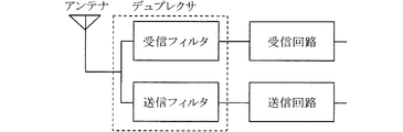
次に、第12の実施形態として通信装置の構成を図15を基に説明する。
図15は上記フィルタを備えたデュプレクサおよび通信装置の構成を示すブロック図である。送信フィルタと受信フィルタとによって、アンテナ共用器としてのデュプレクサを構成している。そして、デュプレクサの送信信号入力ポートに送信回路、受信信号出力ポートに受信回路をそれぞれ接続し、デュプレクサの入出力ポートにアンテナを接続することによって、通信装置の高周波部を構成している。Next, the configuration of a communication apparatus will be described as a twelfth embodiment with reference to FIG.
FIG. 15 is a block diagram illustrating a configuration of a duplexer and a communication device including the filter. The transmission filter and the reception filter constitute a duplexer as an antenna duplexer. Then, a transmission circuit is connected to the transmission signal input port of the duplexer, a reception circuit is connected to the reception signal output port, and an antenna is connected to the input / output port of the duplexer, thereby constituting a high-frequency unit of the communication device.
このように、共振器の段数が多く、且つ小型のフィルタを備えたことにより小型のデュプレクサを構成することができる。また、小型のデュプレクサを備えたことにより小型軽量の通信装置が構成できる。 In this manner, a small duplexer can be configured by providing a large number of resonator stages and including a small filter. In addition, a small and light communication device can be configured by providing a small duplexer.
Claims (10)
前記誘電体コアに貫通孔を形成し、該貫通孔に支持棒を挿通し、該支持棒を前記キャビティに固定することによって、前記キャビティ内部の空間に前記誘電体コアを支持し、
前記キャビティは直方体形状をなし、
前記支持棒は2本または3本あり、各支持棒の両端が前記キャビティの互いに異なる1対の対向する内壁にそれぞれ接合されている多重モード誘電体共振器。A multimode dielectric resonator comprising a dielectric core disposed within a conductive cavity at a predetermined interval from an inner wall surface of the cavity,
Wherein the dielectric core into the through holes are formed, inserting the support rod into the through hole, by fixing the support rod to the cavity, supporting the dielectric core in the cavity inside the space,
The cavity has a rectangular parallelepiped shape,
The multi-mode dielectric resonator includes two or three support rods, and both ends of each support rod are respectively joined to a pair of opposite inner walls of the cavity.
前記誘電体コアに貫通孔を形成し、該貫通孔に支持棒を挿通し、該支持棒を前記キャビティに固定することによって、前記キャビティ内部の空間に前記誘電体コアを支持し、
前記支持棒の少なくとも一部は、前記誘電体コアよりも誘電率の低い誘電体材料からなる多重モード誘電体共振器。A multimode dielectric resonator comprising a dielectric core disposed within a conductive cavity at a predetermined interval from an inner wall surface of the cavity,
Wherein the dielectric core into the through holes are formed, inserting the support rod into the through hole, by fixing the support rod to the cavity, supporting the dielectric core in the cavity inside the space,
At least a part of the support rod is a multimode dielectric resonator made of a dielectric material having a dielectric constant lower than that of the dielectric core .
前記誘電体コアに貫通孔を形成し、該貫通孔に支持棒を挿通し、該支持棒を前記キャビティに固定することによって、前記キャビティ内部の空間に前記誘電体コアを支持し、
前記支持棒は前記誘電体コアよりも誘電率の低い材料からなる中空形状をなし、該中空の内部に導電体が配置されていることを特徴とする多重モード誘電体共振器。A multimode dielectric resonator comprising a dielectric core disposed within a conductive cavity at a predetermined interval from an inner wall surface of the cavity,
Wherein the dielectric core into the through holes are formed, inserting the support rod into the through hole, by fixing the support rod to the cavity, supporting the dielectric core in the cavity inside the space,
The multi-mode dielectric resonator according to claim 1, wherein the support rod has a hollow shape made of a material having a dielectric constant lower than that of the dielectric core, and a conductor is disposed inside the hollow .
前記誘電体コアに貫通孔を形成し、該貫通孔に支持棒を挿通し、該支持棒を前記キャビティに固定することによって、前記キャビティ内部の空間に前記誘電体コアを支持し、
前記貫通孔および前記支持棒は断面がそれぞれ多角形状をなす多重モード誘電体共振器。A multimode dielectric resonator comprising a dielectric core disposed within a conductive cavity at a predetermined interval from an inner wall surface of the cavity,
Wherein the dielectric core into the through holes are formed, inserting the support rod into the through hole, by fixing the support rod to the cavity, supporting the dielectric core in the cavity inside the space,
The through-hole and the support rod are multimode dielectric resonators each having a polygonal cross section .
Applications Claiming Priority (3)
| Application Number | Priority Date | Filing Date | Title |
|---|---|---|---|
| JP2004005341 | 2004-01-13 | ||
| JP2004005341 | 2004-01-13 | ||
| PCT/JP2004/016998 WO2005069425A1 (en) | 2004-01-13 | 2004-11-16 | Multimode dielectric resonator, dielectric filter and communication device |
Publications (2)
| Publication Number | Publication Date |
|---|---|
| JPWO2005069425A1 JPWO2005069425A1 (en) | 2007-07-26 |
| JP4131277B2 true JP4131277B2 (en) | 2008-08-13 |
Family
ID=34792097
Family Applications (1)
| Application Number | Title | Priority Date | Filing Date |
|---|---|---|---|
| JP2005516971A Expired - Fee Related JP4131277B2 (en) | 2004-01-13 | 2004-11-16 | Multimode dielectric resonator, dielectric filter, and communication device |
Country Status (3)
| Country | Link |
|---|---|
| US (2) | US20070152779A1 (en) |
| JP (1) | JP4131277B2 (en) |
| WO (1) | WO2005069425A1 (en) |
Families Citing this family (16)
| Publication number | Priority date | Publication date | Assignee | Title |
|---|---|---|---|---|
| EP2452395B1 (en) | 2009-07-10 | 2013-04-17 | KMW Inc. | Multi-mode resonant filter |
| EP2325940A1 (en) * | 2009-11-19 | 2011-05-25 | Alcatel Lucent | Multi-mode resonant device |
| US20130049890A1 (en) | 2011-08-23 | 2013-02-28 | Mesaplexx Pty Ltd | Multi-mode filter |
| US9406988B2 (en) | 2011-08-23 | 2016-08-02 | Mesaplexx Pty Ltd | Multi-mode filter |
| US20140097913A1 (en) | 2012-10-09 | 2014-04-10 | Mesaplexx Pty Ltd | Multi-mode filter |
| US9325046B2 (en) | 2012-10-25 | 2016-04-26 | Mesaplexx Pty Ltd | Multi-mode filter |
| CN103633402B (en) | 2013-12-16 | 2016-08-17 | 华为技术有限公司 | Duplexer and there is the communication system of this duplexer |
| CN104091985B (en) * | 2014-06-19 | 2016-06-22 | 华南理工大学 | A kind of broadband filter adopting single chamber four mould cavity resonator |
| JP6516492B2 (en) * | 2015-02-05 | 2019-05-22 | 国立大学法人豊橋技術科学大学 | Resonator and high frequency filter using the same |
| BR112019011001B1 (en) * | 2016-11-29 | 2024-01-30 | Huawei Technologies Co., Ltd | FILTER AND COMMUNICATIONS DEVICE |
| JP2020508607A (en) | 2017-02-27 | 2020-03-19 | 華為技術有限公司Huawei Technologies Co.,Ltd. | Multimode resonator with split shamfer |
| CN109037868B (en) * | 2018-08-03 | 2024-04-05 | 华南理工大学 | Single multipath dielectric filter |
| CN109461996B (en) * | 2018-10-10 | 2021-04-30 | 香港凡谷發展有限公司 | Special-shaped cavity three-mode resonance structure and filter comprising same |
| CN113782939B (en) * | 2020-06-09 | 2022-10-28 | 华为技术有限公司 | Dielectric resonator and filter |
| CN111900524B (en) * | 2020-08-07 | 2021-09-03 | 物广系统有限公司 | Resonance unit and dielectric filter |
| RU207446U1 (en) * | 2021-07-12 | 2021-10-28 | Федеральное государственное бюджетное образовательное учреждение высшего образования "Саратовский государственный технический университет имени Гагарина Ю.А." (СГТУ имени Гагарина Ю.А.) | RESONATOR BAND MICROWAVE FILTER |
Family Cites Families (16)
| Publication number | Priority date | Publication date | Assignee | Title |
|---|---|---|---|---|
| JPS5114373A (en) | 1974-07-26 | 1976-02-04 | Yokogawa Electric Works Ltd | RYUSOKUSOKUTEISOCHI |
| JPS5149940A (en) | 1974-10-22 | 1976-04-30 | Takako Fujiwara | Kagaku oyobi goseisenino bosekishino seizoho |
| JPS5622323Y2 (en) * | 1976-05-24 | 1981-05-26 | ||
| JPS58207701A (en) | 1982-05-28 | 1983-12-03 | Murata Mfg Co Ltd | Broad band filter |
| JPH0728168B2 (en) * | 1988-08-24 | 1995-03-29 | 株式会社村田製作所 | Dielectric resonator |
| JPH0812976B2 (en) | 1989-10-26 | 1996-02-07 | 株式会社東芝 | Voltage controlled oscillator |
| US5034711A (en) * | 1990-01-23 | 1991-07-23 | Hughes Aircraft Company | Dielectric resonator support system for a waveguide |
| JPH05129813A (en) * | 1991-11-06 | 1993-05-25 | Murata Mfg Co Ltd | Bush |
| JP3503482B2 (en) * | 1997-09-04 | 2004-03-08 | 株式会社村田製作所 | Multi-mode dielectric resonator device, dielectric filter, composite dielectric filter, combiner, distributor, and communication device |
| JP3506013B2 (en) * | 1997-09-04 | 2004-03-15 | 株式会社村田製作所 | Multi-mode dielectric resonator device, dielectric filter, composite dielectric filter, combiner, distributor, and communication device |
| JP3349476B2 (en) | 1999-08-20 | 2002-11-25 | エヌイーシートーキン株式会社 | Dielectric resonator and dielectric filter |
| JP3465882B2 (en) | 1999-08-20 | 2003-11-10 | Necトーキン株式会社 | Dielectric resonator and dielectric filter |
| JP2002016410A (en) | 2000-06-30 | 2002-01-18 | Tdk Corp | Dielectric resonator |
| JP3985790B2 (en) * | 2003-03-12 | 2007-10-03 | 株式会社村田製作所 | Dielectric resonator device, dielectric filter, composite dielectric filter, and communication device |
| US7044517B2 (en) | 2003-03-14 | 2006-05-16 | Toyoda Gosei Co., Ltd. | Front grille for a vehicle |
| US20040257176A1 (en) * | 2003-05-07 | 2004-12-23 | Pance Kristi Dhimiter | Mounting mechanism for high performance dielectric resonator circuits |
-
2004
- 2004-11-16 JP JP2005516971A patent/JP4131277B2/en not_active Expired - Fee Related
- 2004-11-16 US US10/584,843 patent/US20070152779A1/en not_active Abandoned
- 2004-11-16 WO PCT/JP2004/016998 patent/WO2005069425A1/en active Application Filing
-
2008
- 2008-11-20 US US12/274,883 patent/US7605678B2/en not_active Expired - Fee Related
Also Published As
| Publication number | Publication date |
|---|---|
| JPWO2005069425A1 (en) | 2007-07-26 |
| US20090072929A1 (en) | 2009-03-19 |
| US20070152779A1 (en) | 2007-07-05 |
| WO2005069425A1 (en) | 2005-07-28 |
| US7605678B2 (en) | 2009-10-20 |
Similar Documents
| Publication | Publication Date | Title |
|---|---|---|
| US7605678B2 (en) | Multiple-mode dielectric resonator, dielectric filter, and communication device | |
| JP5260744B2 (en) | Multimode resonant filter | |
| JP3506104B2 (en) | Resonator device, filter, composite filter device, duplexer, and communication device | |
| KR101584707B1 (en) | Multi-mode resonator | |
| US10847861B2 (en) | Multimode resonator | |
| JP2000295010A (en) | Planar general purpose response dual mode cavity filter | |
| JP2007502088A (en) | Mounting mechanism for high performance dielectric resonator circuits. | |
| CN111900524B (en) | Resonance unit and dielectric filter | |
| EP1458051A1 (en) | Dielectric resonator device, dielectric filter, composite dielectric filter, and communication apparatus | |
| KR20170019876A (en) | Resonator of radio frequency filter | |
| JP3633520B2 (en) | Resonator device, filter, duplexer, and communication device | |
| JP2001156511A (en) | Multiple mode dielectric resonator, filter, duplexer and communication device | |
| JP2001345610A (en) | Dielectric resonator, filter, duplexer, and communications equipment | |
| JP3506077B2 (en) | Multi-mode dielectric resonator device, filter, duplexer, and communication device | |
| JP2013168868A (en) | Dielectric resonator and band-pass filter | |
| KR101101745B1 (en) | Assembly of dielectric resonator with high sensitivity using triple mode | |
| KR20150021138A (en) | Triple-mode Filter | |
| JP2007300171A (en) | Band pass filter | |
| JPH09148810A (en) | Band pass filter device | |
| JP2005159597A (en) | Resonator apparatus, filter, duplexer, and communication apparatus | |
| JP4059141B2 (en) | RESONATOR DEVICE, FILTER, COMPOSITE FILTER DEVICE, AND COMMUNICATION DEVICE | |
| JP3788055B2 (en) | Dielectric resonator device, shared transmission and reception device, and communication device | |
| JP4284832B2 (en) | Multimode dielectric resonator device, filter, duplexer, and communication device | |
| KR20130059679A (en) | CERAMIC DUAL MODE RF FILTER USING THE IMAGED HEM(11δ) MADE BY A CONDUCTOR MIRROR SURFACE | |
| JP2009194571A (en) | Multimode dielectric resonator and method of adjusting the same |
Legal Events
| Date | Code | Title | Description |
|---|---|---|---|
| A131 | Notification of reasons for refusal |
Free format text: JAPANESE INTERMEDIATE CODE: A131 Effective date: 20080212 |
|
| A521 | Request for written amendment filed |
Free format text: JAPANESE INTERMEDIATE CODE: A523 Effective date: 20080401 |
|
| TRDD | Decision of grant or rejection written | ||
| A01 | Written decision to grant a patent or to grant a registration (utility model) |
Free format text: JAPANESE INTERMEDIATE CODE: A01 Effective date: 20080430 |
|
| A01 | Written decision to grant a patent or to grant a registration (utility model) |
Free format text: JAPANESE INTERMEDIATE CODE: A01 |
|
| A61 | First payment of annual fees (during grant procedure) |
Free format text: JAPANESE INTERMEDIATE CODE: A61 Effective date: 20080513 |
|
| FPAY | Renewal fee payment (event date is renewal date of database) |
Free format text: PAYMENT UNTIL: 20110606 Year of fee payment: 3 |
|
| R150 | Certificate of patent or registration of utility model |
Free format text: JAPANESE INTERMEDIATE CODE: R150 |
|
| FPAY | Renewal fee payment (event date is renewal date of database) |
Free format text: PAYMENT UNTIL: 20120606 Year of fee payment: 4 |
|
| FPAY | Renewal fee payment (event date is renewal date of database) |
Free format text: PAYMENT UNTIL: 20130606 Year of fee payment: 5 |
|
| FPAY | Renewal fee payment (event date is renewal date of database) |
Free format text: PAYMENT UNTIL: 20130606 Year of fee payment: 5 |
|
| LAPS | Cancellation because of no payment of annual fees |